JP6865794B2 - Composition for semiconductor resist and pattern formation method using it - Google Patents
Composition for semiconductor resist and pattern formation method using it Download PDFInfo
- Publication number
- JP6865794B2 JP6865794B2 JP2019140074A JP2019140074A JP6865794B2 JP 6865794 B2 JP6865794 B2 JP 6865794B2 JP 2019140074 A JP2019140074 A JP 2019140074A JP 2019140074 A JP2019140074 A JP 2019140074A JP 6865794 B2 JP6865794 B2 JP 6865794B2
- Authority
- JP
- Japan
- Prior art keywords
- substituted
- carbon atoms
- unsubstituted
- group
- groups
- Prior art date
- Legal status (The legal status is an assumption and is not a legal conclusion. Google has not performed a legal analysis and makes no representation as to the accuracy of the status listed.)
- Active
Links
Images


Classifications
-
- G—PHYSICS
- G03—PHOTOGRAPHY; CINEMATOGRAPHY; ANALOGOUS TECHNIQUES USING WAVES OTHER THAN OPTICAL WAVES; ELECTROGRAPHY; HOLOGRAPHY
- G03F—PHOTOMECHANICAL PRODUCTION OF TEXTURED OR PATTERNED SURFACES, e.g. FOR PRINTING, FOR PROCESSING OF SEMICONDUCTOR DEVICES; MATERIALS THEREFOR; ORIGINALS THEREFOR; APPARATUS SPECIALLY ADAPTED THEREFOR
- G03F7/00—Photomechanical, e.g. photolithographic, production of textured or patterned surfaces, e.g. printing surfaces; Materials therefor, e.g. comprising photoresists; Apparatus specially adapted therefor
- G03F7/004—Photosensitive materials
-
- G—PHYSICS
- G03—PHOTOGRAPHY; CINEMATOGRAPHY; ANALOGOUS TECHNIQUES USING WAVES OTHER THAN OPTICAL WAVES; ELECTROGRAPHY; HOLOGRAPHY
- G03F—PHOTOMECHANICAL PRODUCTION OF TEXTURED OR PATTERNED SURFACES, e.g. FOR PRINTING, FOR PROCESSING OF SEMICONDUCTOR DEVICES; MATERIALS THEREFOR; ORIGINALS THEREFOR; APPARATUS SPECIALLY ADAPTED THEREFOR
- G03F7/00—Photomechanical, e.g. photolithographic, production of textured or patterned surfaces, e.g. printing surfaces; Materials therefor, e.g. comprising photoresists; Apparatus specially adapted therefor
- G03F7/0035—Multiple processes, e.g. applying a further resist layer on an already in a previously step, processed pattern or textured surface
Description
本発明は、半導体レジスト用組成物およびこれを用いたパターン形成方法に関する。 The present invention relates to a composition for a semiconductor resist and a pattern forming method using the same.
次世代の半導体デバイスを製造するための要素技術の一つとして、EUV(極端紫外線)リソグラフィが注目されている。EUVリソグラフィは、露光光源として波長13.5nmのEUVを用いるパターン形成技術である。EUVリソグラフィによれば、半導体デバイス製造プロセスの露光工程で、極めて微細なパターン(例えば、20nm以下)を形成することができるのが実証されている。 EUV (extreme ultraviolet) lithography is drawing attention as one of the elemental technologies for manufacturing next-generation semiconductor devices. EUV lithography is a pattern forming technique that uses EUV with a wavelength of 13.5 nm as an exposure light source. According to EUV lithography, it has been demonstrated that extremely fine patterns (for example, 20 nm or less) can be formed in the exposure process of the semiconductor device manufacturing process.
極端紫外線(extreme ultraviolet、EUV)リソグラフィの実現は、16nm以下の空間解像度(spatial resolutions)で遂行できる互換可能なフォトレジストの現像を必要とする。現在、伝統的な化学増幅型(CA:chemically amplified)フォトレジストは、次世代デバイスのための解像度(resolution)、光速度(photospeed)、およびフィーチャー粗さ(feature roughness、ラインエッジ粗さ(line edge roughnessまたはLER)とも呼ばれる)に対する仕様を充足させるために開発が行われている。 The realization of extreme ultraviolet (EUV) lithography requires the development of compatible photoresists that can be performed at spatial resolutions of 16 nm or less. Currently, traditional chemically amplified photoresists are used for resolution, speed of light, and feature roughness and line edge roughness for next-generation devices. Development is being carried out to satisfy the specifications for (also called roughness or LER)).
高分子型フォトレジストで起こる酸触媒反応に起因した固有の画像ぼやけ(intrinsic image blur)は、小さいフィーチャー(feature)大きさで解像度を制限し、これは電子ビーム(e−beam)リソグラフィにおいて長い間知らされてきた事実である。化学増幅型(CA)フォトレジストは、高い感度(sensitivity)のために設計されたが、これらの典型的な元素構成が13.5nmの波長の光でフォトレジストの吸光度を低くし、その結果、感度を減少させるため、部分的にはEUV露光下で、さらに微細パターンの形成が困難になることがある。 Intrinsic image blur caused by acid-catalyzed reactions in polymeric photoresists limits resolution with small feature sizes, which has long been in electron beam (e-beam) lithography. It is a fact that has been informed. Chemically amplified (CA) photoresists have been designed for high sensitivity, but their typical elemental composition reduces the absorbance of the photoresist with light at a wavelength of 13.5 nm, resulting in Due to the reduced sensitivity, it may be more difficult to form finer patterns, partly under EUV exposure.
CAフォトレジストはまた、小さいフィーチャー大きさにおいて粗さ(roughness)問題によって、微細パターンの形成が困難になることがある。部分的に酸触媒工程の本質に起因して、光速度(photospeed)が減少することによってラインエッジ粗さ(LER)が増加するのが実験で確認された。CAフォトレジストの欠点および問題に起因して、半導体産業では新たな類型の高性能フォトレジストに対する要求がある。 CA photoresists can also make it difficult to form fine patterns due to roughness problems at small feature sizes. Experiments have confirmed that the line edge roughness (LER) increases as the speed of light decreases, partly due to the nature of the acid-catalyzed process. Due to the shortcomings and problems of CA photoresists, there is a demand for new types of high performance photoresists in the semiconductor industry.
本発明の目的は、エッチング耐性および感度に優れ、取り扱いが容易な半導体レジスト用組成物を提供することにある。 An object of the present invention is to provide a composition for a semiconductor resist, which has excellent etching resistance and sensitivity and is easy to handle.
本発明の他の目的は、前記半導体レジスト用組成物を用いたパターン形成方法を提供することにある。 Another object of the present invention is to provide a pattern forming method using the composition for semiconductor resist.
本発明の一実施形態による半導体レジスト用組成物は、下記化学式1で表される有機金属化合物、および溶媒を含む。 The composition for a semiconductor resist according to one embodiment of the present invention contains an organometallic compound represented by the following chemical formula 1 and a solvent.
上記化学式1中、
R1は、置換もしくは非置換の炭素数1〜20のアルキル基、置換もしくは非置換の炭素数3〜20のシクロアルキル基、置換もしくは非置換の炭素数2〜20のアルケニル基、置換もしくは非置換の炭素数2〜20のアルキニル基、置換もしくは非置換の炭素数3〜20のアルケニルアルキル基、置換もしくは非置換の炭素数3〜20のアルキニルアルキル基、置換もしくは非置換の炭素数6〜30のアリール基、置換もしくは非置換の炭素数7〜30のアリールアルキル基、または−Rc−O−Rd(ここで、Rcは、置換または非置換の炭素数1〜20のアルキレン基であり、Rdは、置換または非置換の炭素数1〜20のアルキル基である)であり、
R2〜R4は、それぞれ独立して、−ORaまたは−OC(=O)Rbであり、
この際、Raは、置換もしくは非置換の炭素数1〜20のアルキル基、置換もしくは非置換の炭素数3〜20のシクロアルキル基、置換もしくは非置換の炭素数2〜20のアルケニル基、置換もしくは非置換の炭素数2〜20のアルキニル基、置換もしくは非置換の炭素数6〜30のアリール基、置換もしくは非置換の炭素数7〜30のアリールアルキル基、またはこれらの組み合わせであり、
Rbは、水素原子、置換もしくは非置換の炭素数1〜20のアルキル基、置換もしくは非置換の炭素数3〜20のシクロアルキル基、置換もしくは非置換の炭素数2〜20のアルケニル基、置換もしくは非置換の炭素数2〜20のアルキニル基、置換もしくは非置換の炭素数6〜30のアリール基、置換もしくは非置換の炭素数7〜30のアリールアルキル基、またはこれらの組み合わせである。
In the above chemical formula 1,
R 1 is a substituted or unsubstituted alkyl group having 1 to 20 carbon atoms, a substituted or unsubstituted cycloalkyl group having 3 to 20 carbon atoms, a substituted or unsubstituted alkenyl group having 2 to 20 carbon atoms, a substituted or unsubstituted alkenyl group. Substituted alkynyl groups with 2 to 20 carbon atoms, substituted or unsubstituted alkenylalkyl groups with 3 to 20 carbon atoms, substituted or unsubstituted alkynylalkyl groups with 3 to 20 carbon atoms, substituted or unsubstituted alkynylalkyl groups with 6 to 20 carbon atoms 30 aryl groups, substituted or unsubstituted arylalkyl groups having 7 to 30 carbon atoms, or -R c- O-R d (where R c is a substituted or unsubstituted alkylene group having 1 to 20 carbon atoms. R d is a substituted or unsubstituted alkyl group having 1 to 20 carbon atoms).
R 2 to R 4 are independently −OR a or −OC (= O) R b , respectively.
At this time, Ra is a substituted or unsubstituted alkyl group having 1 to 20 carbon atoms, a substituted or unsubstituted cycloalkyl group having 3 to 20 carbon atoms, a substituted or unsubstituted alkenyl group having 2 to 20 carbon atoms, and the like. A substituted or unsubstituted alkynyl group having 2 to 20 carbon atoms, a substituted or unsubstituted aryl group having 6 to 30 carbon atoms, a substituted or unsubstituted arylalkyl group having 7 to 30 carbon atoms, or a combination thereof.
Rb is a hydrogen atom, a substituted or unsubstituted alkyl group having 1 to 20 carbon atoms, a substituted or unsubstituted cycloalkyl group having 3 to 20 carbon atoms, a substituted or unsubstituted alkenyl group having 2 to 20 carbon atoms, A substituted or unsubstituted alkynyl group having 2 to 20 carbon atoms, a substituted or unsubstituted aryl group having 6 to 30 carbon atoms, a substituted or unsubstituted arylalkyl group having 7 to 30 carbon atoms, or a combination thereof.
本発明の他の一実施形態によるパターン形成方法は、基板の上にエッチング対象膜を形成する段階、前記エッチング対象膜の上に前述の半導体レジスト用組成物を塗布してフォトレジスト膜を形成する段階、前記フォトレジスト膜をパターニングしてフォトレジストパターンを形成する段階、および前記フォトレジストパターンをエッチングマスクとして用いて前記エッチング対象膜をエッチングする段階を含む。 The pattern forming method according to another embodiment of the present invention is a step of forming an etching target film on a substrate, and a photoresist film is formed by applying the above-mentioned semiconductor resist composition on the etching target film. The step includes a step of patterning the photoresist film to form a photoresist pattern, and a step of etching the etching target film using the photoresist pattern as an etching mask.
本発明による半導体レジスト用組成物は、相対的にエッチング耐性および感度に優れて取り扱いが容易であるので、これを用いれば感度および限界解像度に優れ、高い縦横比を有していてもパターンが崩れないフォトレジストパターンを提供することができる。 Since the composition for semiconductor resist according to the present invention is relatively excellent in etching resistance and sensitivity and easy to handle, it is excellent in sensitivity and limit resolution, and the pattern is broken even if it has a high aspect ratio. No photoresist pattern can be provided.
以下、添付した図面を参照して本発明の実施例を詳細に説明する。但し、本記載を説明することにおいて、既に公知された機能あるいは構成に関する説明は、本記載の要旨を明瞭にするために省略する。 Hereinafter, examples of the present invention will be described in detail with reference to the attached drawings. However, in explaining this description, the description regarding the functions or configurations already known will be omitted for the sake of clarifying the gist of this description.
本記載を明確に説明するために説明上不必要な部分を省略し、明細書全体にわたって同一または類似の構成要素については同一な参照符号を付ける。また、図面に示された各構成の大きさおよび厚さは説明の便宜のために任意に示したので、本記載が必ずしも図示されたものに限定されるのではない。 In order to clarify this description, unnecessary parts are omitted, and the same or similar components are designated by the same reference numerals throughout the specification. Moreover, since the size and thickness of each configuration shown in the drawings are arbitrarily shown for convenience of explanation, this description is not necessarily limited to those shown in the drawings.
図面で様々な層および領域を明確に表現するために、厚さを拡大して示した。そして、図面で説明の便宜のために一部層および領域の厚さを誇張して示した。層、膜、領域、板などの部分が他の部分「の上に」または「上に」あるというとき、これは他の部分の「真上に」ある場合だけでなく、その中間にまた他の部分がある場合も含む。 The thickness has been enlarged to clearly represent the various layers and regions in the drawings. Then, for convenience of explanation, the thickness of some layers and regions is exaggerated in the drawings. When parts such as layers, membranes, regions, plates, etc. are "above" or "above" other parts, this is not only when they are "directly above" other parts, but also in between. Including the case where there is a part of.
本明細書で、「置換」とは、水素原子が重水素、ハロゲン基、ヒドロキシ基、アミノ基、置換もしくは非置換の炭素数1〜30の第1〜第4級アミノ基、ニトロ基、置換もしくは非置換の炭素数1〜40のシリル基、炭素数1〜30のアルキル基、炭素数1〜10のハロアルキル基、炭素数1〜10のアルキルシリル基、炭素数3〜30のシクロアルキル基、炭素数6〜30のアリール基、炭素数1〜20のアルコキシ基、またはシアノ基で置換されたことを意味する。「非置換」とは、水素原子が他の置換基で置換されず水素原子として残っていることを意味する。 As used herein, the term "substitution" means that the hydrogen atom is a heavy hydrogen, a halogen group, a hydroxy group, an amino group, a substituted or unsubstituted primary to quaternary amino group having 1 to 30 carbon atoms, a nitro group, or a substituent. Alternatively, an unsubstituted silyl group having 1 to 40 carbon atoms, an alkyl group having 1 to 30 carbon atoms, a haloalkyl group having 1 to 10 carbon atoms, an alkylsilyl group having 1 to 10 carbon atoms, and a cycloalkyl group having 3 to 30 carbon atoms. , It means that it was substituted with an aryl group having 6 to 30 carbon atoms, an alkoxy group having 1 to 20 carbon atoms, or a cyano group. "Unsubstituted" means that a hydrogen atom is not substituted with another substituent and remains as a hydrogen atom.
本明細書で、「アルキル(alkyl)基」とは、別途の定義がない限り、直鎖型または分枝鎖型脂肪族炭化水素基を意味する。アルキル基は、いかなる二重結合や三重結合を含んでいない「飽和アルキル基」であり得る。 As used herein, the term "alkyl group" means a linear or branched aliphatic hydrocarbon group, unless otherwise defined. The alkyl group can be a "saturated alkyl group" that does not contain any double or triple bonds.
前記アルキル基は、炭素数1〜20のアルキル基であり得る。より具体的に、アルキル基は、炭素数1〜10のアルキル基、または炭素数1〜6のアルキル基であり得る。例えば、炭素数1〜4のアルキル基は、アルキル鎖に1〜4個の炭素原子が含まれるものを意味し、メチル基、エチル基、プロピル基、イソプロピル基、n−ブチル基、イソブチル基、sec−ブチル基、およびt−ブチル基からなる群より選択されるものを示す。 The alkyl group can be an alkyl group having 1 to 20 carbon atoms. More specifically, the alkyl group can be an alkyl group having 1 to 10 carbon atoms or an alkyl group having 1 to 6 carbon atoms. For example, an alkyl group having 1 to 4 carbon atoms means that the alkyl chain contains 1 to 4 carbon atoms, and a methyl group, an ethyl group, a propyl group, an isopropyl group, an n-butyl group, an isobutyl group, and the like. The one selected from the group consisting of sec-butyl group and t-butyl group is shown.
前記アルキル基は、具体的な例を挙げれば、メチル基、エチル基、プロピル基、イソプロピル基、ブチル基、イソブチル基、t−ブチル基、ペンチル基、ヘキシル基、シクロプロピル基、シクロブチル基、シクロペンチル基、シクロヘキシル基などを意味する。 Specific examples of the alkyl group include methyl group, ethyl group, propyl group, isopropyl group, butyl group, isobutyl group, t-butyl group, pentyl group, hexyl group, cyclopropyl group, cyclobutyl group and cyclopentyl group. It means a group, a cyclohexyl group, etc.
本明細書で、「シクロアルキル(cycloalkyl)基」とは、別途の定義がない限り、1価の環状脂肪族炭化水素基を意味する。 As used herein, the term "cycloalkyl group" means a monovalent cyclic aliphatic hydrocarbon group unless otherwise defined.
本明細書で、「アリール(aryl)基」とは、環状の置換基の全ての元素がp−軌道を有しており、これらp−軌道が共役(conjugation)を形成している置換基を意味し、単環または縮合多環(即ち、炭素原子の隣接した対を共有する環)官能基を含む。 As used herein, the term "aryl group" refers to a substituent in which all the elements of the cyclic substituent have a p-orbital and these p-orbitals form a condensation. Means that it comprises a monocyclic or condensed polycyclic (ie, a ring that shares adjacent pairs of carbon atoms) functional group.
本発明の一実施形態による半導体レジスト用組成物は、有機金属化合物および溶媒を含む。 The composition for a semiconductor resist according to one embodiment of the present invention contains an organometallic compound and a solvent.
有機金属化合物は、中心に位置する金属原子に多様な有機基が結合されているものであって、下記化学式1で表される。 The organometallic compound is one in which various organic groups are bonded to a metal atom located at the center, and is represented by the following chemical formula 1.
上記化学式1中、
R1は、置換もしくは非置換の炭素数1〜20のアルキル基、置換もしくは非置換の炭素数3〜20のシクロアルキル基、置換もしくは非置換の炭素数2〜20のアルケニル基、置換もしくは非置換の炭素数2〜20のアルキニル基、置換もしくは非置換の炭素数3〜20のアルケニルアルキル基、置換もしくは非置換の炭素数3〜20のアルキニルアルキル基、置換もしくは非置換の炭素数6〜30のアリール基、置換もしくは非置換の炭素数7〜30のベンジルアリールアルキル基、および−Rc−O−Rd(ここで、Rcは、置換または非置換の炭素数1〜20のアルキレン基であり、Rdは、置換または非置換の炭素数1〜20のアルキル基である)の中から選択され、
R2〜R4は、それぞれ独立して、−ORaまたは−OC(=O)Rbであり、
この際、Raは、置換もしくは非置換の炭素数1〜20のアルキル基、置換もしくは非置換の炭素数3〜20のシクロアルキル基、置換もしくは非置換の炭素数2〜20のアルケニル基、置換もしくは非置換の炭素数2〜20のアルキニル基、置換もしくは非置換の炭素数6〜30のアリール基、置換もしくは非置換の炭素数7〜30のアリールアルキル基、またはこれらの組み合わせであり、
Rbは、水素原子、置換もしくは非置換の炭素数1〜20のアルキル基、置換もしくは非置換の炭素数3〜20のシクロアルキル基、置換もしくは非置換の炭素数2〜20のアルケニル基、置換もしくは非置換の炭素数2〜20のアルキニル基、置換もしくは非置換の炭素数6〜30のアリール基、置換もしくは非置換の炭素数7〜30のアリールアルキル基、またはこれらの組み合わせである。
In the above chemical formula 1,
R 1 is a substituted or unsubstituted alkyl group having 1 to 20 carbon atoms, a substituted or unsubstituted cycloalkyl group having 3 to 20 carbon atoms, a substituted or unsubstituted alkenyl group having 2 to 20 carbon atoms, substituted or unsubstituted. Substituted alkynyl groups with 2 to 20 carbon atoms, substituted or unsubstituted alkenylalkyl groups with 3 to 20 carbon atoms, substituted or unsubstituted alkynylalkyl groups with 3 to 20 carbon atoms, substituted or unsubstituted alkynylalkyl groups with 6 to 20 carbon atoms 30 aryl groups, substituted or unsubstituted benzylarylalkyl groups having 7 to 30 carbon atoms, and -R c- O-R d (where R c is a substituted or unsubstituted alkylene having 1 to 20 carbon atoms. It is a group, and R d is a substituted or unsubstituted alkyl group having 1 to 20 carbon atoms).
R 2 to R 4 are independently −OR a or −OC (= O) R b , respectively.
At this time, Ra is a substituted or unsubstituted alkyl group having 1 to 20 carbon atoms, a substituted or unsubstituted cycloalkyl group having 3 to 20 carbon atoms, a substituted or unsubstituted alkenyl group having 2 to 20 carbon atoms, and the like. A substituted or unsubstituted alkynyl group having 2 to 20 carbon atoms, a substituted or unsubstituted aryl group having 6 to 30 carbon atoms, a substituted or unsubstituted arylalkyl group having 7 to 30 carbon atoms, or a combination thereof.
Rb is a hydrogen atom, a substituted or unsubstituted alkyl group having 1 to 20 carbon atoms, a substituted or unsubstituted cycloalkyl group having 3 to 20 carbon atoms, a substituted or unsubstituted alkenyl group having 2 to 20 carbon atoms, A substituted or unsubstituted alkynyl group having 2 to 20 carbon atoms, a substituted or unsubstituted aryl group having 6 to 30 carbon atoms, a substituted or unsubstituted arylalkyl group having 7 to 30 carbon atoms, or a combination thereof.
本発明の一実施形態において、R1は、Snと結合して有機溶媒に対する溶解度を向上させることができる。本発明の一実施形態において、R1は、極端紫外線露光時に、Sn−R1結合が解離されてラジカルを生成することができる。例えば、R1は、置換もしくは非置換の炭素数1〜10のアルキル基、置換もしくは非置換の炭素数3〜20のシクロアルキル基、置換もしくは非置換の炭素数3〜20のアルケニル基、置換もしくは非置換の炭素数3〜20のアルキニル基、置換もしくは非置換の炭素数3〜20のアルケニルアルキル基、置換もしくは非置換の炭素数3〜20のアルキニルアルキル基、置換もしくは非置換の炭素数6〜30のアリール基、置換もしくは非置換の炭素数7〜30のアリールアルキル基、および−Rc−O−Rd(ここで、Rcは、置換または非置換の炭素数1〜20のアルキレン基であり、Rdは、置換または非置換の炭素数1〜20のアルキル基である)の中から選択できる。 In one embodiment of the invention, R 1 can bind to Sn to improve its solubility in organic solvents. In one embodiment of the present invention, R 1 can generate radicals by dissociating the Sn—R 1 bond during extreme ultraviolet exposure. For example, R 1 is a substituted or unsubstituted alkyl group having 1 to 10 carbon atoms, a substituted or unsubstituted cycloalkyl group having 3 to 20 carbon atoms, a substituted or unsubstituted alkenyl group having 3 to 20 carbon atoms, or a substituted alkenyl group. Alternatively, an unsubstituted or unsubstituted alkynyl group having 3 to 20 carbon atoms, a substituted or unsubstituted alkenylalkyl group having 3 to 20 carbon atoms, a substituted or unsubstituted alkynylalkyl group having 3 to 20 carbon atoms, or a substituted or unsubstituted alkynyl alkyl group. 6 to 30 aryl groups, substituted or unsubstituted arylalkyl groups having 7 to 30 carbon atoms, and -R c- O-R d (where R c is substituted or unsubstituted having 1 to 20 carbon atoms. It is an alkylene group, and R d can be selected from substituted or unsubstituted alkyl groups having 1 to 20 carbon atoms).
本発明の一実施形態において、前記Raは、置換もしくは非置換の炭素数1〜10のアルキル基、置換もしくは非置換の炭素数3〜20のシクロアルキル基、置換もしくは非置換の炭素数2〜8のアルケニル基、置換もしくは非置換の炭素数2〜8のアルキニル基、および置換もしくは非置換の炭素数7〜30のアリールアルキル基の中から選択され、
前記Rbは、水素原子、置換もしくは非置換の炭素数1〜10のアルキル基、置換もしくは非置換の炭素数3〜20のシクロアルキル基、置換もしくは非置換の炭素数2〜8のアルケニル基、置換もしくは非置換の炭素数2〜8のアルキニル基、および置換もしくは非置換の炭素数7〜30のアリールアルキル基の中から選択される。
In one embodiment of the invention, the Ra is a substituted or unsubstituted alkyl group having 1 to 10 carbon atoms, a substituted or unsubstituted cycloalkyl group having 3 to 20 carbon atoms, a substituted or unsubstituted alkyl group having 2 carbon atoms. Selected from ~ 8 alkenyl groups, substituted or unsubstituted alkynyl groups having 2 to 8 carbon atoms, and substituted or unsubstituted arylalkyl groups having 7 to 30 carbon atoms.
The R b is a hydrogen atom, a substituted or unsubstituted alkyl group having 1 to 10 carbon atoms, a substituted or unsubstituted cycloalkyl group having 3 to 20 carbon atoms, or an substituted or unsubstituted alkenyl group having 2 to 8 carbon atoms. , A substituted or unsubstituted alkynyl group having 2 to 8 carbon atoms, and a substituted or unsubstituted arylalkyl group having 7 to 30 carbon atoms are selected.
本発明の一実施形態において、R2〜R4は、前述のR1とは異なり、Snに金属−酸素結合を付与する。本発明の一実施形態において、R2〜R4のうちの少なくとも一つは−OC(=O)Rbであり得る。具体的に、R2〜R4のうちの少なくとも二つ以上は−OC(=O)Rbであり得る。さらに具体的に、R2〜R4が全て−OC(=O)Rbであり得る。R2〜R4のうちの少なくとも一つが−OC(=O)Rbを含む場合、これを含む半導体レジスト組成物を用いて形成されたパターンは、優れた感度および限界解像度を示すことができる。 In one embodiment of the present invention, R 2 to R 4 impart a metal-oxygen bond to Sn, unlike R 1 described above. In one embodiment of the invention, at least one of R 2 to R 4 can be -OC (= O) R b . Specifically, at least two or more of R 2 to R 4 can be −OC (= O) R b . More specifically, R 2 to R 4 can all be −OC (= O) R b . When at least one of R 2 to R 4 contains -OC (= O) R b , the pattern formed using the semiconductor resist composition containing the -OC (= O) R b can exhibit excellent sensitivity and limit resolution. ..
但し、本発明はこれに限定されるものではなく、R2〜R4のうちの少なくとも一つが−ORaであるか、R2〜R4が全て−ORaであり得る。 However, the present invention is not limited to this, or at least one of R 2 to R 4 is -OR a, may be R 2 to R 4 are all -OR a.
本発明の一実施形態において、RaおよびRbは、それぞれ独立して、置換もしくは非置換の炭素数1〜10のアルキル基、置換もしくは非置換の炭素数3〜20のシクロアルキル基、置換もしくは非置換の炭素数2〜8のアルケニル基、置換もしくは非置換の炭素数2〜8のアルキニル基、置換もしくは非置換の炭素数7〜30のアリールアルキル基、またはこれらの組み合わせの中から選択できる。 In one embodiment of the invention, Ra and R b are independently substituted or unsubstituted alkyl groups having 1 to 10 carbon atoms, substituted or unsubstituted cycloalkyl groups having 3 to 20 carbon atoms, and substituted. Alternatively, select from an unsubstituted alkenyl group having 2 to 8 carbon atoms, a substituted or unsubstituted alkynyl group having 2 to 8 carbon atoms, a substituted or unsubstituted arylalkyl group having 7 to 30 carbon atoms, or a combination thereof. it can.
前述の化学式1で示される有機金属化合物は有機錫化合物であって、錫は波長13.5nmの極端紫外線を強く吸収することができるので、高エネルギーを有する光に対する感度が優れる。したがって、本発明の一実施形態による有機錫化合物は、従来の有機および/または無機レジストに比べて優れた安定性および感度を示すことができる。 The organometallic compound represented by the above-mentioned chemical formula 1 is an organotin compound, and since tin can strongly absorb extreme ultraviolet rays having a wavelength of 13.5 nm, it has excellent sensitivity to light having high energy. Therefore, the organotin compounds according to one embodiment of the present invention can exhibit superior stability and sensitivity as compared with conventional organic and / or inorganic resists.
一方、本発明の一実施形態において、前記有機金属化合物は、下記化学式2〜化学式4で表される化合物のうちの少なくとも一つであり得る。 On the other hand, in one embodiment of the present invention, the organometallic compound can be at least one of the compounds represented by the following chemical formulas 2 to 4.
上記化学式2〜化学式4中、
R1は、それぞれ独立して、置換もしくは非置換の炭素数1〜20のアルキル基、置換もしくは非置換の炭素数3〜20のシクロアルキル基、置換もしくは非置換の炭素数2〜20のアルケニル基、置換もしくは非置換の炭素数2〜20のアルキニル基、置換もしくは非置換の炭素数3〜20のアルケニルアルキル基、置換もしくは非置換の炭素数3〜20のアルキニルアルキル基、置換もしくは非置換の炭素数6〜30のアリール基、置換もしくは非置換の炭素数7〜30のアリールアルキル基、および−Rc−O−Rd(ここで、Rcは、置換または非置換の炭素数1〜20のアルキレン基であり、Rdは、置換または非置換の炭素数1〜20のアルキル基である)の中から選択され、
R12、R13、R14、およびR33は、それぞれ独立して、置換もしくは非置換の炭素数1〜10のアルキル基、置換もしくは非置換の炭素数3〜20のシクロアルキル基、置換もしくは非置換の炭素数2〜8のアルケニル基、置換もしくは非置換の炭素数2〜8のアルキニル基、および置換もしくは非置換の炭素数7〜30のアリールアルキル基の中から選択され、
R22、R23、R24、R32、およびR34は、それぞれ独立して、水素原子、置換もしくは非置換の炭素数1〜10のアルキル基、置換もしくは非置換の炭素数3〜20のシクロアルキル基、置換もしくは非置換の炭素数2〜8のアルケニル基、置換もしくは非置換の炭素数2〜8のアルキニル基、および置換もしくは非置換の炭素数7〜30のアリールアルキル基の中から選択される。
In the above chemical formulas 2 to 4,
R 1 is an independently substituted or unsubstituted alkyl group having 1 to 20 carbon atoms, substituted or unsubstituted cycloalkyl group having 3 to 20 carbon atoms, and substituted or unsubstituted alkenyl having 2 to 20 carbon atoms. Group, substituted or unsubstituted alkynyl group having 2 to 20 carbon atoms, substituted or unsubstituted alkenylalkyl group having 3 to 20 carbon atoms, substituted or unsubstituted alkynylalkyl group having 3 to 20 carbon atoms, substituted or unsubstituted 6 to 30 carbon atoms, substituted or unsubstituted arylalkyl groups having 7 to 30 carbon atoms, and -R c- O-R d (where R c is substituted or unsubstituted carbon number 1). ~ 20 alkylene groups, R d is a substituted or unsubstituted alkyl group having 1 to 20 carbon atoms).
R 12 , R 13 , R 14 and R 33 are independently substituted or unsubstituted alkyl groups having 1 to 10 carbon atoms, substituted or unsubstituted cycloalkyl groups having 3 to 20 carbon atoms, substituted or unsubstituted. Selected from unsubstituted alkenyl groups having 2 to 8 carbon atoms, substituted or unsubstituted alkynyl groups having 2 to 8 carbon atoms, and substituted or unsubstituted arylalkyl groups having 7 to 30 carbon atoms.
R 22 , R 23 , R 24 , R 32 , and R 34 are independently hydrogen atoms, substituted or unsubstituted alkyl groups having 1 to 10 carbon atoms, and substituted or unsubstituted alkyl groups having 3 to 20 carbon atoms, respectively. Among cycloalkyl groups, substituted or unsubstituted alkenyl groups having 2 to 8 carbon atoms, substituted or unsubstituted alkynyl groups having 2 to 8 carbon atoms, and substituted or unsubstituted arylalkyl groups having 7 to 30 carbon atoms. Be selected.
具体的に、前記R1は、置換もしくは非置換の炭素数1〜10のアルキル基、置換もしくは非置換の炭素数3〜20のシクロアルキル基、置換もしくは非置換の炭素数3〜20のアルケニルアルキル基、置換もしくは非置換の炭素数3〜20のアルキニルアルキル基、および−Rc−O−Rd(ここで、Rcは、置換または非置換の炭素数1〜20のアルキレン基であり、Rdは、置換または非置換の炭素数1〜20のアルキル基である)の中から選択されるいずれか一つであり得る。 Specifically, the R 1 is a substituted or unsubstituted alkyl group having 1 to 10 carbon atoms, a substituted or unsubstituted cycloalkyl group having 3 to 20 carbon atoms, or a substituted or unsubstituted alkenyl having 3 to 20 carbon atoms. Alkyl groups, substituted or unsubstituted alkynyl alkyl groups having 3 to 20 carbon atoms, and -R c- O-R d (where R c is a substituted or unsubstituted alkylene group having 1 to 20 carbon atoms. , R d can be any one selected from substituted or unsubstituted alkyl groups having 1 to 20 carbon atoms).
具体的に、一実施形態による有機金属化合物は、下記化学式5〜化学式13で表される化合物のうちの少なくとも一つであり得る。 Specifically, the organometallic compound according to one embodiment can be at least one of the compounds represented by the following chemical formulas 5 to 13.
一般に使用される有機レジストの場合、エッチング耐性が不足して、高い縦横比のパターンが崩れる恐れがある。 In the case of a commonly used organic resist, the etching resistance may be insufficient and the pattern with a high aspect ratio may be broken.
また、従来の無機レジスト(例えば、メタルオキシド化合物)の場合、高い腐食性を有する硫酸と過酸化水素との混合物を使用するため、取り扱いが難しく保存安定性が悪く、混合物として性能改善のための構成変更が相対的に難しく、高濃度の現像液を使用しなければならない。 Further, in the case of a conventional inorganic resist (for example, a metal oxide compound), since a mixture of sulfuric acid and hydrogen peroxide having high corrosiveness is used, it is difficult to handle and the storage stability is poor, and the performance of the mixture is improved. It is relatively difficult to change the configuration, and a high-concentration developer must be used.
これに対し、本発明の一実施形態による半導体レジスト用組成物は、前述のように有機金属化合物が、中心金属原子に多様な有機基が結合された構造を有する。これによって、既存の有機および/または無機レジストに比べて、相対的にエッチング耐性および感度に優れ、取り扱いが容易である。 On the other hand, the composition for a semiconductor resist according to one embodiment of the present invention has a structure in which an organometallic compound has various organic groups bonded to a central metal atom as described above. As a result, it has relatively excellent etching resistance and sensitivity as compared with existing organic and / or inorganic resists, and is easy to handle.
具体的には、前記化学式1で表される有機金属化合物において、中心金属元素に金属−酸素結合以外に、R1のような脂肪族炭化水素基または−アルキル−O−アルキルのような官能基が結合されている場合、溶媒に対する溶解度が改善され、極端紫外線で露光する際にSn−R1結合が解離されて、ラジカルを生成することができる。これにより、本発明の半導体レジスト用組成物を用いて、優れた感度および限界解像度を有するパターンを形成することができる。 Specifically, in the organometallic compound represented by the chemical formula 1, in addition to the metal-oxygen bond to the central metal element, an aliphatic hydrocarbon group such as R 1 or a functional group such as -alkyl-O-alkyl when is coupled, improved solubility in solvents, extreme ultraviolet Sn-R 1 bonds when exposed at is dissociated, it is possible to generate a radical. Thereby, the semiconductor resist composition of the present invention can be used to form a pattern having excellent sensitivity and limit resolution.
また、本発明の一実施形態による半導体レジスト用組成物を用いて形成されたパターンは、高い縦横比(aspect ratio)を有していても崩れにくい。 Further, the pattern formed by using the composition for semiconductor resist according to the embodiment of the present invention does not easily collapse even if it has a high aspect ratio.
本発明の一実施形態による半導体レジスト組成物において、前記化学式1で表される有機金属化合物は、組成物の全体質量を基準にして、0.01質量%〜10質量%の含有量で含まれることが好ましい。このような含有量で含まれる場合、保管安定性に優れ、薄膜形成が容易である。 In the semiconductor resist composition according to the embodiment of the present invention, the organometallic compound represented by the chemical formula 1 is contained in a content of 0.01% by mass to 10% by mass based on the total mass of the composition. Is preferable. When it is contained in such a content, it is excellent in storage stability and easy to form a thin film.
上記有機金属化合物は、市販品を用いてもよいし合成品を用いてもよい。合成方法としては、従来公知の方法を適宜採用することができる。 As the organometallic compound, a commercially available product or a synthetic product may be used. As the synthesis method, a conventionally known method can be appropriately adopted.
本発明の一実施形態による半導体レジスト用組成物は、前述の有機金属化合物と溶媒とを含むことが好ましい。 The composition for a semiconductor resist according to one embodiment of the present invention preferably contains the above-mentioned organometallic compound and a solvent.
本発明の一実施形態による半導体レジスト組成物に含まれる溶媒は、有機溶媒であり得る。その例としては、例えば、芳香族化合物類(例えば、キシレン、トルエン等)、アルコール類(例えば、4−メチル−2−ペンタノール、4−メチル−2−プロパノール、1−ブタノール、メタノール、イソプロピルアルコール、1−プロパノール等)、エーテル類(例えば、アニソール、テトラヒドロフラン等)、エステル類(n−ブチルアセテート、プロピレングリコールモノメチルエーテルアセテート、エチルアセテート、エチルラクテート等)、ケトン類(例えば、メチルエチルケトン、2−ヘプタノン等)、またはこれらの混合物などを含むことができるが、これらに限定されるものではない。 The solvent contained in the semiconductor resist composition according to the embodiment of the present invention may be an organic solvent. Examples include aromatic compounds (eg, xylene, toluene, etc.), alcohols (eg, 4-methyl-2-pentanol, 4-methyl-2-propanol, 1-butanol, methanol, isopropyl alcohol). , 1-propanol, etc.), ethers (eg, anisole, tetrahydrofuran, etc.), esters (n-butyl acetate, propylene glycol monomethyl ether acetate, ethyl acetate, ethyl lactate, etc.), ketones (eg, methyl ethyl ketone, 2-heptanone, etc.) Etc.), or a mixture thereof, etc., but is not limited to these.
本発明の一実施形態による半導体レジスト組成物は、有機金属化合物と溶媒以外に、追加的に樹脂をさらに含むことができる。 The semiconductor resist composition according to one embodiment of the present invention may further contain a resin in addition to the organometallic compound and the solvent.
このような樹脂としては、下記グループ1に示す芳香族部分を少なくとも1つ含むフェノール系樹脂であり得る。 Such a resin may be a phenolic resin containing at least one aromatic moiety shown in Group 1 below.
前記樹脂は、重量平均分子量が500〜20,000であり得る。 The resin can have a weight average molecular weight of 500 to 20,000.
前記樹脂は、前記半導体レジスト用組成物の総質量に対して、0.1質量%〜50質量%で含まれ得る。 The resin may be contained in an amount of 0.1% by mass to 50% by mass with respect to the total mass of the composition for semiconductor resist.
前記樹脂の含有量が上記範囲である場合、優れたエッチング耐性および耐熱性を有することができる。 When the content of the resin is in the above range, it can have excellent etching resistance and heat resistance.
本発明の一実施形態による半導体レジスト用組成物は、前述の有機金属化合物、溶媒、および樹脂からなることが好ましい。但し、前述の実施形態による半導体レジスト用組成物は、場合によって添加剤をさらに含むことができる。前記添加剤としては、例えば、界面活性剤、架橋剤、レべリング剤、またはこれらの組み合わせが挙げられる。 The composition for a semiconductor resist according to one embodiment of the present invention preferably comprises the above-mentioned organometallic compound, solvent, and resin. However, the composition for semiconductor resist according to the above-described embodiment may further contain additives in some cases. Examples of the additive include a surfactant, a cross-linking agent, a leveling agent, or a combination thereof.
界面活性剤としては、例えば、アルキルベンゼンスルホン酸塩、アルキルピリジニウム塩、ポリエチレングリコール、第4級アンモニウム塩、またはこれらの組み合わせを使用することができるが、これらに限定されるものではない。 As the surfactant, for example, alkylbenzene sulfonate, alkylpyridinium salt, polyethylene glycol, quaternary ammonium salt, or a combination thereof can be used, but the surfactant is not limited thereto.
架橋剤は、例えば、メラミン系の架橋剤、置換尿素系の架橋剤、またはポリマー系の架橋剤などが挙げられるが、これらに限定されるものではない。少なくとも2つの架橋形成置換基を有する架橋剤として、例えば、メトキシメチル化グリコールウリル、ブトキシメチル化グリコールウリル、メトキシメチル化メラミン、ブトキシメチル化メラミン、メトキシメチル化ベンゾグアナミン、ブトキシメチル化ベンゾグアナミン、メトキシメチル化尿素、ブトキシメチル化尿素、またはメトキシメチル化チオ尿素などの化合物を使用することができる。 Examples of the cross-linking agent include, but are not limited to, a melamine-based cross-linking agent, a substituted urea-based cross-linking agent, and a polymer-based cross-linking agent. Cross-linking agents having at least two cross-linking substituents include, for example, methoxymethylated glycol uryl, butoxymethylated glycol uryl, methoxymethylated melamine, butoxymethylated melamine, methoxymethylated benzoguanamine, butoxymethylated benzoguanamine, methoxymethylated. Compounds such as urea, butoxymethylated urea, or methoxymethylated thiourea can be used.
レベリング剤は、印刷(塗布)時にコーティング膜の平坦性を向上させるためのものであって、商業的な方法で入手可能な公知のレベリング剤を使用することができる。 The leveling agent is for improving the flatness of the coating film at the time of printing (coating), and a known leveling agent available by a commercially available method can be used.
これら添加剤の使用量は、所望の物性によって容易に調節することができ、適宜設定できる。 The amount of these additives used can be easily adjusted according to desired physical properties and can be appropriately set.
また、本発明の半導体レジスト用組成物は、基板との密着力などの向上のために(例えば、半導体レジスト用組成物の基板との接着力向上のために)、接着力向上剤としてシランカップリング剤を添加剤としてさらに使用することができる。記シランカップリング剤としては、例えば、ビニルトリメトキシシラン、ビニルトリエトキシシラン、ビニルトリクロロシラン、ビニルトリス(β−メトキシエトキシ)シラン;3−メタクリルオキシプロピルトリメトキシシラン、3−アクリルオキシプロピルトリメトキシシラン、p−スチリルトリメトキシシラン、3−メタクリルオキシプロピルメチルジメトキシシラン、3−メタクリルオキシプロピルメチルジエトキシシランなどの炭素−炭素不飽和結合含有シラン化合物;トリメトキシ[3−(フェニルアミノ)プロピル]シランなどを使用することができるが、これらに限定されるものではない。 Further, the composition for semiconductor resist of the present invention is a silane cup as an adhesive strength improving agent for improving the adhesive strength with the substrate (for example, for improving the adhesive strength of the composition for semiconductor resist with the substrate). The ring agent can be further used as an additive. Examples of the silane coupling agent include vinyltrimethoxysilane, vinyltriethoxysilane, vinyltrichlorosilane, vinyltris (β-methoxyethoxy) silane; 3-methacryloxypropyltrimethoxysilane, and 3-acrylicoxypropyltrimethoxysilane. , P-styryltrimethoxysilane, 3-methacryloxypropylmethyldimethoxysilane, 3-methacryloxypropylmethyldiethoxysilane and other carbon-carbon unsaturated bond-containing silane compounds; trimethoxy [3- (phenylamino) propyl] silane, etc. Can be used, but is not limited to these.
本発明の半導体レジスト用組成物は、高い縦横比を有するパターンを形成しても、パターン崩壊が発生しないか、パターン崩壊が発生する危険を大きく減らすことができる。したがって、例えば、5nm〜100nmの線幅を有する微細パターン、例えば、5nm〜80nmの線幅を有する微細パターン、例えば、5nm〜70nmの線幅を有する微細パターン、例えば、5nm〜50nmの線幅を有する微細パターン、例えば、5nm〜40nmの線幅を有する微細パターン、例えば、5nm〜30nmの線幅を有する微細パターン、例えば、5nm〜20nmの線幅を有する微細パターンを形成するために、波長5nm〜150nmの光を使用するフォトレジスト工程、例えば波長5nm〜100nmの光を使用するフォトレジスト工程、例えば波長5nm〜80nmの光を使用するフォトレジスト工程、例えば波長5nm〜50nmの光を使用するフォトレジスト工程、例えば波長5nm〜30nmの光を使用するフォトレジスト工程、例えば波長5nm〜20nmの光を使用するフォトレジスト工程に、本発明の組成物を使用することができる。したがって、本発明の一実施形態による半導体レジスト用組成物を用いれば、波長13.5nmのEUV光源を使用する極端紫外線リソグラフィを実現することができる。 Even if a pattern having a high aspect ratio is formed, the composition for a semiconductor resist of the present invention does not cause pattern collapse or can greatly reduce the risk of pattern collapse. Therefore, for example, a fine pattern having a line width of 5 nm to 100 nm, for example, a fine pattern having a line width of 5 nm to 80 nm, for example, a fine pattern having a line width of 5 nm to 70 nm, for example, a line width of 5 nm to 50 nm. To form a fine pattern having, for example, a fine pattern having a line width of 5 nm to 40 nm, for example, a fine pattern having a line width of 5 nm to 30 nm, for example, a fine pattern having a line width of 5 nm to 20 nm, a wavelength of 5 nm. A photoresist step using light from ~ 150 nm, eg, a photoresist step using light from 5 nm to 100 nm, eg, a photoresist step using light from 5 nm to 80 nm, eg, a photo using light from 5 nm to 50 nm. The composition of the present invention can be used in a resisting step, for example, a photoresist step using light having a wavelength of 5 nm to 30 nm, for example, a photoresist step using light having a wavelength of 5 nm to 20 nm. Therefore, by using the composition for semiconductor resist according to one embodiment of the present invention, extreme ultraviolet lithography using an EUV light source having a wavelength of 13.5 nm can be realized.
本発明の他の一実施形態によれば、前述の半導体レジスト用組成物を使用してパターンを形成する方法を提供する。一例として、製造されたパターンはフォトレジストパターンであり得る。 According to another embodiment of the present invention, there is provided a method of forming a pattern using the above-mentioned composition for semiconductor resist. As an example, the manufactured pattern can be a photoresist pattern.
本発明の一実施形態によるパターン形成方法は、基板上にエッチング対象膜を形成する段階、前記エッチング対象膜の上に前述の半導体レジスト用組成物を適用してフォトレジスト膜を形成する段階、前記フォトレジスト膜をパターニングしてフォトレジストパターンを形成する段階、および前記フォトレジストパターンをエッチングマスクとして用いて前記エッチング対象膜をエッチングする段階を含む。 The pattern forming method according to one embodiment of the present invention includes a step of forming an etching target film on a substrate, a step of applying the above-mentioned semiconductor resist composition on the etching target film to form a photoresist film, and the above. It includes a step of patterning a photoresist film to form a photoresist pattern, and a step of etching the etching target film using the photoresist pattern as an etching mask.
以下、前述の半導体レジスト用組成物を使用してパターンを形成する方法について図1〜5を参照して説明する。図1〜図5は、本発明による半導体レジスト用組成物を用いたパターン形成方法を説明するための断面概略図である。 Hereinafter, a method of forming a pattern using the above-mentioned composition for semiconductor resist will be described with reference to FIGS. 1 to 5. 1 to 5 are schematic cross-sectional views for explaining a pattern forming method using the composition for semiconductor resist according to the present invention.
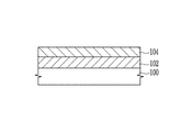
図1を参照すれば、先ず、エッチング対象物を準備する。前記エッチング対象物の例としては、半導体基板100上に形成される薄膜102であり得る。以下、エッチング対象物が薄膜102である場合に限定して説明するが、本発明は本実施形態に限定されない。薄膜102上に残留する汚染物などを除去するために、薄膜102の表面を洗浄する。薄膜102は、例えば、シリコン窒化膜、ポリシリコン膜、またはシリコン酸化膜であり得る。
Referring to FIG. 1, first, an object to be etched is prepared. An example of the object to be etched may be a
次いで、洗浄された薄膜102の表面上にレジスト下層膜104を形成するためのレジスト下層膜形成用組成物を、スピンコーティング法を適用してコーティングする。但し、本発明の形態がこれに限定されるものではなく、公知の多様なコーティング法、例えばスプレーコーティング法、ディップコーティング法、ナイフエッジコーティング法、印刷法、例えばインクジェット印刷法およびスクリーン印刷法などを用いることもできる。
Next, a composition for forming a resist
レジスト下層膜形成用組成物をコーティングする工程は省略してもよい。以下では、レジスト下層膜を形成する場合について説明する。 The step of coating the resist underlayer film forming composition may be omitted. The case of forming the resist underlayer film will be described below.
コーティング後、乾燥およびベーキング工程を行って、薄膜102上にレジスト下層膜104を形成する。ベーキング処理は例えば100〜500℃、例えば100℃〜300℃の温度で行うことができる。
After coating, a drying and baking step is performed to form a resist
レジスト下層膜104は、基板100とフォトレジスト膜106との間に形成され、基板100とフォトレジスト膜106との界面または層間ハードマスク(hardmask)から反射される照射線が、意図していないフォトレジスト領域に散乱される場合、フォトレジスト線幅(linewidth)の不均一性およびパターン形成性を妨害するのを防止することができる。
The resist
図2を参照すれば、レジスト下層膜104の上に、前述の半導体レジスト用組成物をコーティングしてフォトレジスト膜106を形成する。フォトレジスト膜106は、基板100上に形成された薄膜102の上に、前述の半導体レジスト用組成物を、コーティングした後に熱処理工程により硬化させた形態であり得る。
Referring to FIG. 2, the resist
より具体的には、半導体レジスト用組成物を使用してパターンを形成する段階は、前述の半導体レジスト用組成物を、薄膜102が形成された基板100上にスピンコーティング法、スリットコーティング法、インクジェット印刷などで塗布する工程、および塗布された半導体レジスト用組成物を乾燥してフォトレジスト膜106を形成する工程、を含むことができる。
More specifically, at the stage of forming a pattern using the composition for semiconductor resist, the above-mentioned composition for semiconductor resist is applied onto the
半導体レジスト用組成物については既に詳しく説明したので、重複する説明は省略する。 Since the composition for semiconductor resist has already been described in detail, a duplicate description will be omitted.
次いで、フォトレジスト膜106が形成されている基板100を加熱する第1ベーキング工程を行う。第1ベーキング工程は、80℃〜120℃の温度で行うことができる。
Next, a first baking step is performed in which the
図3を参照すれば、フォトレジスト膜106を選択的に露光する。
With reference to FIG. 3, the
一例として、露光工程で使用できる光の例としては、i線(i−line)(波長365nm)、KrFエキシマレーザ(波長248nm)、ArFエキシマレーザ(波長193nm)などの短波長を有する光だけでなく、極端紫外線(EUV、Extreme UltraViolet;波長13.5nm)、E−Beam(電子ビーム)などの高エネルギー波長を有する光なども例示できる。 As an example, examples of light that can be used in the exposure process include only light having a short wavelength such as i-line (wavelength 365 nm), KrF excimer laser (wavelength 248 nm), and ArF excimer laser (wavelength 193 nm). However, light having a high energy wavelength such as extreme ultraviolet (EUV, Extreme UltraViolet; wavelength 13.5 nm) and E-Beam (electron beam) can also be exemplified.
より具体的に、本発明の一実施形態による露光用の光は、波長5nm〜150nmの範囲を有する短波長光であり得、極端紫外線(波長13.5nm)、E−Beam(電子ビーム)などの高エネルギー波長を有する光であり得る。 More specifically, the light for exposure according to one embodiment of the present invention may be short wavelength light having a wavelength in the range of 5 nm to 150 nm, such as extreme ultraviolet light (wavelength 13.5 nm), E-Beam (electron beam), and the like. Can be light having a high energy wavelength of.
フォトレジスト膜106中の露光領域106aは、有機金属化合物間の縮合などの架橋反応によって重合体を形成することにより、フォトレジスト膜106の未露光領域106bと互いに異なる溶解度を有するようになる。
The exposed region 106a in the
次いで、基板100に第2ベーキング工程を行う。第2ベーキング工程は、90℃〜200℃の温度で行うことができる。第2ベーキング工程を行うことによって、フォトレジスト膜106の露光領域106aは、現像液への溶解が起こり難い状態となる。
Next, the
図4には、現像液を用いて未露光領域に該当するフォトレジスト膜106bを溶解させて除去することによって形成された、フォトレジストパターン108が示されている。具体的には、2−ヘプタノンなどの有機溶媒を使用して、未露光領域に該当するフォトレジスト膜106bを溶解させた後に除去することによって、ネガティブトーンイメージに該当するフォトレジストパターン108が完成される。
FIG. 4 shows a
前述のように、本発明の一実施形態によるパターン形成方法で使用される現像液は、有機溶媒であり得る。本発明の一実施形態によるパターン形成方法で使用される有機溶媒の例としては、メチルエチルケトン、アセトン、シクロヘキサノン、2−ヘプタノンなどのケトン類、4−メチル−2−プロパノール、1−ブタノール、イソプロパノール、1−プロパノール、メタノールなどのアルコール類、プロピレングリコールモノメチルエステルアセテート、酢酸エチル、乳酸エチル、酢酸n−ブチル、ブチロラクトンなどのエステル類、ベンゼン、キシレン、トルエンなどの芳香族化合物、またはこれらの組み合わせ等が挙げられる。 As described above, the developer used in the pattern forming method according to the embodiment of the present invention can be an organic solvent. Examples of the organic solvent used in the pattern forming method according to the embodiment of the present invention include ketones such as methyl ethyl ketone, acetone, cyclohexanone and 2-heptanone, 4-methyl-2-propanol, 1-butanol, isopropanol, 1 -Alcohols such as propanol and methanol, esters such as propylene glycol monomethyl ester acetate, ethyl acetate, ethyl lactate, n-butyl acetate and butyrolactone, aromatic compounds such as benzene, xylene and toluene, or combinations thereof. Be done.
但し、本発明の一実施形態によるフォトレジストパターンが、ネガティブトーンイメージとして形成されることに必ずしも制限されず、ポジティブトーンイメージを有するように形成され得る。この場合、ポジティブトーンイメージ形成のために使用できる現像剤としては、テトラエチルアンモニウムヒドロキシド、テトラプロピルアンモニウムヒドロキシド、テトラブチルアンモニウムヒドロキシドまたはこれらの組み合わせなどの第4級アンモニウムヒドロキシドなどが挙げられる。 However, the photoresist pattern according to one embodiment of the present invention is not necessarily limited to being formed as a negative tone image, and may be formed so as to have a positive tone image. In this case, examples of the developer that can be used for forming a positive tone image include tetraethylammonium hydroxide, tetrapropylammonium hydroxide, quaternary ammonium hydroxide such as tetrabutylammonium hydroxide or a combination thereof.
前述のように、i線(波長365nm)、KrFエキシマレーザ(波長248nm)、ArFエキシマレーザ(波長193nm)などの波長を有する光だけでなく、極端紫外線(EUV、Extreme UltraViolet;波長13.5nm)、E−Beam(電子ビーム)などの高エネルギーを有する光などによって露光されて形成されたフォトレジストパターン108は、5nm〜100nmの線幅を有することができる。一例として、フォトレジストパターン108は、5nm〜90nm、5nm〜80nm、5nm〜70nm、5nm〜60nm、10nm〜50nm、10nm〜40nm、10nm〜30nm、10nm〜20nmの線幅で形成され得る。
As described above, not only light having wavelengths such as i-line (wavelength 365 nm), KrF excimer laser (wavelength 248 nm), ArF excimer laser (wavelength 193 nm), but also extreme ultraviolet (EUV, Extreme UltraViolet; wavelength 13.5 nm). The
フォトレジストパターン108は、50nm以下、例えば40nm以下、例えば30nm以下、例えば25nm以下のハーフピッチ、および10nm以下、5nm以下の線幅粗さを有するピッチを有することができる。
The
次いで、フォトレジストパターン108をエッチングマスクにして、レジスト下層膜104をエッチングする。前記のようなエッチング工程で有機膜パターン112が形成され、形成された有機膜パターン112もフォトレジストパターン108に対応する幅を有することができる。
Next, the
図5を参照すれば、フォトレジストパターン108をエッチングマスクとして適用して、露光された薄膜102をエッチングする。その結果、薄膜は薄膜パターン114として形成される。
Referring to FIG. 5, the
前記薄膜102のエッチングは、例えばエッチングガスを用いた乾式エッチングで行うことができ、エッチングガスは、例えばCHF3、CF4、Cl2、BCl3およびこれらの混合ガス等を使用することができる。
The etching of the
EUV光源を使用して行われた露光工程により形成されたフォトレジストパターン108を用いて形成された薄膜パターン114は、フォトレジストパターン108に対応する幅を有することができる。一例として、フォトレジストパターン108と同様に5nm〜100nmの線幅を有することができる。例えば、EUV光源を使用して行われた露光工程によって形成された薄膜パターン114は、フォトレジストパターン108と同様に、5nm〜90nm、5nm〜80nm、5nm〜70nm、5nm〜60nm、10nm〜50nm、10nm〜40nm、10nm〜30nm、10nm〜20nmの線幅を有することができ、より具体的に20nm以下の線幅で形成され得る。
The
以下、有機金属化合物の合成およびこれを含む半導体レジスト用組成物の製造に関する実施例を通じて、本発明をさらに詳しく説明する。しかし、下記実施例によって本発明が技術的に限定されるのではない。 Hereinafter, the present invention will be described in more detail through examples relating to the synthesis of an organometallic compound and the production of a composition for a semiconductor resist containing the same. However, the following examples do not technically limit the present invention.
(合成例1)
下記化学式A−1で表される化合物(10g、25.6mmol)に25mlの酢酸を常温で徐々に滴下した後、110℃で24時間加熱還流した。
(Synthesis Example 1)
After gradually adding 25 ml of acetic acid to the compound represented by the following chemical formula A-1 (10 g, 25.6 mmol) at room temperature, the mixture was heated under reflux at 110 ° C. for 24 hours.
その後、温度を常温に下げた後、酢酸を真空蒸留して、下記化学式5で表される化合物を得た(収率:90%)。 Then, after lowering the temperature to room temperature, acetic acid was vacuum distilled to obtain a compound represented by the following chemical formula 5 (yield: 90%).
(合成例2)
下記化学式A−2で表される化合物(10g、25.4mmol)に25mlのアクリル酸を常温で徐々に滴下した後、80℃で6時間加熱還流した。
(Synthesis Example 2)
After gradually adding 25 ml of acrylic acid to the compound represented by the following chemical formula A-2 (10 g, 25.4 mmol) at room temperature, the mixture was heated under reflux at 80 ° C. for 6 hours.
その後、温度を常温に下げた後、アクリル酸を真空蒸留して、下記化学式6で表される化合物を得た(収率:50%)。 Then, after lowering the temperature to room temperature, acrylic acid was vacuum-distilled to obtain a compound represented by the following chemical formula 6 (yield: 50%).
(合成例3)
下記化学式A−3で表される化合物(10g、23.7mmol)に25mlのプロピオン酸を常温で徐々に滴下した後、110℃で24時間加熱還流した。
(Synthesis Example 3)
25 ml of propionic acid was gradually added dropwise to the compound represented by the following chemical formula A-3 (10 g, 23.7 mmol) at room temperature, and then heated under reflux at 110 ° C. for 24 hours.
その後、温度を常温に下げた後、アクリル酸を真空蒸留して、下記化学式7で表される化合物を得た(収率:95%)。 Then, after lowering the temperature to room temperature, acrylic acid was vacuum distilled to obtain a compound represented by the following chemical formula 7 (yield: 95%).
(合成例4)
前記合成例2の化学式A−2で表される化合物(10g、25.4mmol)に、25mlのイソブチル酸を常温で徐々に滴下した後、110℃で24時間加熱還流した。
(Synthesis Example 4)
To the compound represented by the chemical formula A-2 of Synthesis Example 2, 25 ml of isobutyl acid was gradually added dropwise at room temperature, and then the mixture was heated under reflux at 110 ° C. for 24 hours.
その後、温度を常温に下げた後、イソブチル酸を真空蒸留して、下記化学式8で表される化合物を得た(収率:95%)。 Then, after lowering the temperature to room temperature, isobutyl acid was vacuum-distilled to obtain a compound represented by the following chemical formula 8 (yield: 95%).
(合成例5)
下記化学式A−4で表される化合物(10g、24.6mmol)に、25mlのプロピオン酸を常温で徐々に滴下した後、110℃で24時間加熱還流した。
(Synthesis Example 5)
25 ml of propionic acid was gradually added dropwise to the compound represented by the following chemical formula A-4 (10 g, 24.6 mmol) at room temperature, and then heated under reflux at 110 ° C. for 24 hours.
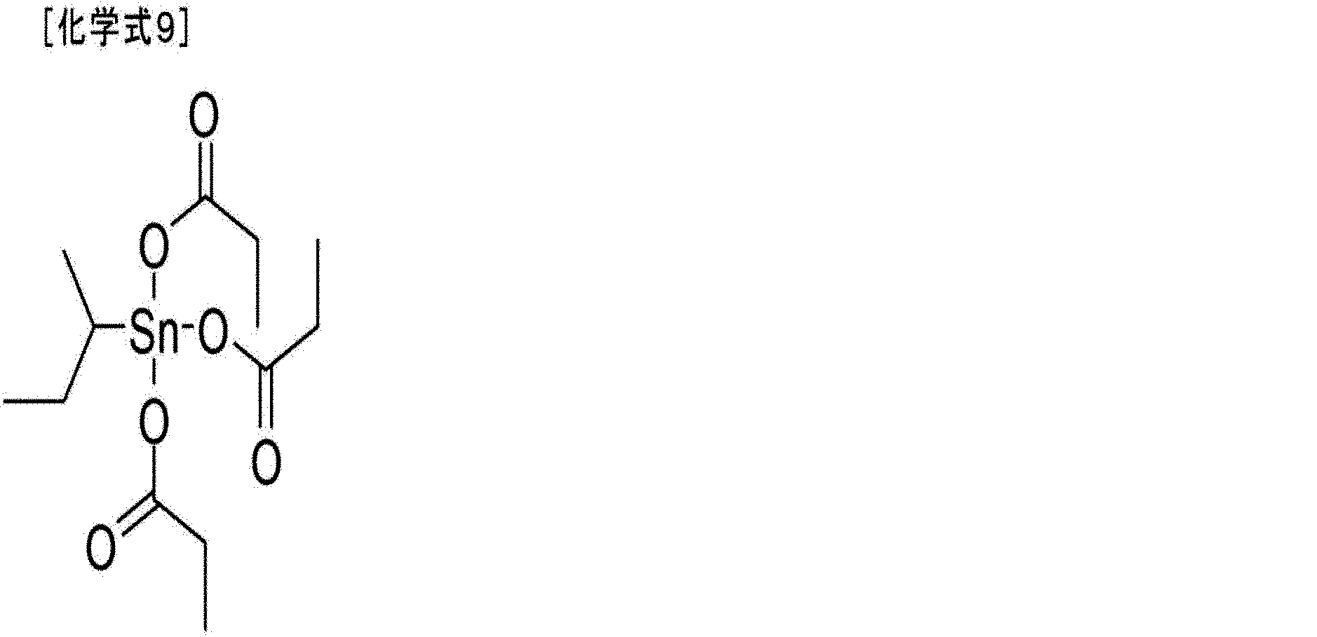
その後、温度を常温に下げた後、アクリル酸を真空蒸留して、下記化学式9で表される化合物を得た(収率:90%)。 Then, after lowering the temperature to room temperature, acrylic acid was vacuum distilled to obtain a compound represented by the following chemical formula 9 (yield: 90%).
(合成例6)
前述の化学式A−1で表される化合物(10g、24.6mmol)を50mLのCH2Cl2に溶かし、4M HClジエチルエーテル溶液(3当量、36.9mmol)を−78℃で30分間徐々に滴下した。その後、常温で12時間攪拌し、溶媒を濃縮して、下記化学式A−5で表される化合物を得た(収率:80%)。
(Synthesis Example 6)
The compound represented by the above chemical formula A-1 (10 g, 24.6 mmol) is dissolved in 50 mL of CH 2 Cl 2 , and a 4M HCl diethyl ether solution (3 equivalents, 36.9 mmol) is gradually added at −78 ° C. for 30 minutes. Dropped. Then, the mixture was stirred at room temperature for 12 hours, and the solvent was concentrated to obtain a compound represented by the following chemical formula A-5 (yield: 80%).
前記化学式A−5で表される化合物(10g、35.4mmol)を無水ペンタン30mlに溶かし、温度を0℃に下げた。その後、ジエチルアミン(7.8g、106.3mmol)を徐々に滴下した後、t−BuOH(7.9g、106.3mmol)を添加し、常温で1時間攪拌した。反応終了後、ろ過して濃縮し、その後真空乾燥して、下記化学式10で表される化合物を得た(収率:60%)。 The compound represented by the chemical formula A-5 (10 g, 35.4 mmol) was dissolved in 30 ml of anhydrous pentane, and the temperature was lowered to 0 ° C. Then, diethylamine (7.8 g, 106.3 mmol) was gradually added dropwise, t-BuOH (7.9 g, 106.3 mmol) was added, and the mixture was stirred at room temperature for 1 hour. After completion of the reaction, the mixture was filtered and concentrated, and then vacuum dried to obtain a compound represented by the following chemical formula 10 (yield: 60%).
(合成例7)
前述の化学式A−5で表される化合物の合成工程で、前述の化学式A−1で表される化合物の代わりに前述の化学式A−2で表される化合物を使用したことを除いては同様の方法で、下記化学式A−6で表される化合物を得た(収率:75%)。
(Synthesis Example 7)
The same applies except that the compound represented by the above-mentioned chemical formula A-2 is used in place of the above-mentioned compound represented by the chemical formula A-1 in the step of synthesizing the compound represented by the above-mentioned chemical formula A-5. A compound represented by the following chemical formula A-6 was obtained by the above method (yield: 75%).
前記化学式A−6で表される化合物(10g、37.3mmol)を無水ペンタンに溶かし、温度を0℃に下げた。その後、ジエチルアミン(8.2g、111.9mmol)を徐々に滴下し、次いで、イソプロパノール(6.7g、111.9mmol)を添加し、常温で1時間攪拌した。反応終了後、ろ過して濃縮し、真空乾燥して、下記化学式11で表される化合物を得た(収率:65%)。 The compound represented by the chemical formula A-6 (10 g, 37.3 mmol) was dissolved in anhydrous pentane, and the temperature was lowered to 0 ° C. Then, diethylamine (8.2 g, 111.9 mmol) was gradually added dropwise, then isopropanol (6.7 g, 111.9 mmol) was added, and the mixture was stirred at room temperature for 1 hour. After completion of the reaction, the mixture was filtered, concentrated, and vacuum dried to obtain a compound represented by the following chemical formula 11 (yield: 65%).
(合成例8)
前述の化学式A−5で表される化合物の合成工程で、前述の化学式A−1で表される化合物の代わりに前述の化学式A−3で表される化合物を使用したことを除いては同様の方法で、下記化学式A−7で表される化合物を得た(収率:70%)。
(Synthesis Example 8)
The same applies except that the compound represented by the above-mentioned chemical formula A-3 is used in place of the above-mentioned compound represented by the chemical formula A-1 in the step of synthesizing the compound represented by the above-mentioned chemical formula A-5. A compound represented by the following chemical formula A-7 was obtained by the above method (yield: 70%).
前記化学式A−7で表される化合物(10g、18.7mmol)を無水ペンタンに溶かし、温度を0℃に下げた。その後、ジエチルアミン(7.4g、101.3mmol)を徐々に滴下した後、エタノール(6.1g、101.3mmol)を添加し、常温で1時間攪拌した。反応終了後、ろ過して濃縮し、真空乾燥して、下記化学式12で表される化合物を得た(収率:60%)。 The compound represented by the chemical formula A-7 (10 g, 18.7 mmol) was dissolved in anhydrous pentane, and the temperature was lowered to 0 ° C. Then, diethylamine (7.4 g, 101.3 mmol) was gradually added dropwise, ethanol (6.1 g, 101.3 mmol) was added, and the mixture was stirred at room temperature for 1 hour. After completion of the reaction, the mixture was filtered, concentrated, and vacuum dried to obtain a compound represented by the following chemical formula 12 (yield: 60%).
(合成例9)
下記化学式A−2で表される化合物(10g、25.4mmol)に25mlのギ酸を常温で徐々に滴下した後、100℃で24時間加熱還流した。
(Synthesis Example 9)
After gradually adding 25 ml of formic acid to the compound represented by the following chemical formula A-2 (10 g, 25.4 mmol) at room temperature, the mixture was heated under reflux at 100 ° C. for 24 hours.
その後、温度を常温に下げた後、アクリル酸を真空蒸留して、下記化学式13で表される化合物を得た(収率:90%)。 Then, after lowering the temperature to room temperature, acrylic acid was vacuum distilled to obtain a compound represented by the following chemical formula 13 (yield: 90%).
(比較合成例)
ジブチル錫ジクロリド(Dibutyltin dichloride、10g、33mmol)を30mLのエーテルに溶かした後、1Mの水酸化ナトリウム(NaOH)水溶液70mLを添加し、1時間攪拌した。攪拌後、生成された固体をろ過して脱イオン水25mLで3回洗浄した後、100℃で減圧乾燥を行って、下記化学式14で表される重量平均分子量1,500の有機金属化合物を得た。
(Comparative synthesis example)
Dibutyltin dichloride (10 g, 33 mmol) was dissolved in 30 mL of ether, 70 mL of 1 M aqueous sodium hydroxide (NaOH) solution was added, and the mixture was stirred for 1 hour. After stirring, the produced solid is filtered, washed three times with 25 mL of deionized water, and then dried under reduced pressure at 100 ° C. to obtain an organometallic compound having a weight average molecular weight of 1,500 represented by the following chemical formula 14. It was.
(実施例1〜9)
合成例1〜9で合成された有機金属化合物をそれぞれキシレン(xylene)に2質量%の濃度で溶かした後、0.1μmPTFEシリンジフィルターでろ過して、実施例1〜9の半導体レジスト用組成物を製造した。
(Examples 1 to 9)
The organometallic compounds synthesized in Synthesis Examples 1 to 9 are each dissolved in xylene at a concentration of 2% by mass, and then filtered through a 0.1 μm PTFE syringe filter to form the composition for semiconductor resist of Examples 1 to 9. Manufactured.
自然酸化膜表面を有する4インチ円形シリコンウェハーを、薄膜フィルム蒸着のための基板として準備し、前記基板をUVオゾンクリーニングシステム下で10分間前処理した。その後、実施例1〜9による半導体用レジスト組成物を、前処理された基板上に、1500rpmで30秒間スピンコーティングした。ホットプレート上で、基板を100℃で120秒間焼成(塗布後焼成、post−apply bake、PAB)して、薄膜を形成した。 A 4-inch circular silicon wafer having a natural oxide film surface was prepared as a substrate for thin film film deposition, and the substrate was pretreated under a UV ozone cleaning system for 10 minutes. Then, the resist composition for semiconductors according to Examples 1 to 9 was spin-coated on the pretreated substrate at 1500 rpm for 30 seconds. On the hot plate, the substrate was fired at 100 ° C. for 120 seconds (baking after coating, post-apply bucket, PAB) to form a thin film.
コーティングおよびベーキング後、エリプソメーターにより測定した薄膜の厚さは約40nmであった。 After coating and baking, the thickness of the thin film measured by an ellipsometer was about 40 nm.
(比較例)
比較合成例で合成された上記化学式14で表される化合物を、4−メチル−2−ペンタノール(4−methyl−2−pentanol)に1質量%の濃度で溶かした後、0.1μmPTFEシリンジフィルターでろ過して半導体レジスト用組成物を製造した。
(Comparison example)
The compound represented by the above chemical formula 14 synthesized in the comparative synthesis example is dissolved in 4-methyl-2-pentanol at a concentration of 1% by mass, and then a 0.1 μm PTFE syringe filter is used. A composition for a semiconductor resist was produced by filtering with.
その後、製造された比較例による半導体レジスト用組成物に対して前述の実施例と同一の工程を経て基板の上に薄膜を形成した。 Then, a thin film was formed on the substrate of the manufactured composition for semiconductor resist according to the comparative example through the same steps as in the above-mentioned Examples.
コーティングおよびベーキング後、エリプソメーターにより測定した薄膜の厚さは約40nmであった。 After coating and baking, the thickness of the thin film measured by an ellipsometer was about 40 nm.
(評価1)
直径が500μmである50個の円形パッド直線アレイをEUV光(Lawrence Berkeley National Laboratory Micro Exposure Tool、MET)を使用して、実施例1〜9および比較例のレジストがコーティングされたウェハーに投射した。パッド露光時間を調節して、EUV増加線量が各パッドに適用されるようにした。
(Evaluation 1)
A linear array of 50 circular pads with a diameter of 500 μm was projected onto wafers coated with resists from Examples 1-9 and Comparative Examples using EUV light (Lawence Berkeley National Laboratory Micro Exposure Tool, MET). The pad exposure time was adjusted so that the EUV increased dose was applied to each pad.
その後、レジストおよび基板をホットプレート上で、150℃、120秒間の露光後焼成(post−exposure bake、PEB)を行った。焼成された薄膜を現像液(2−ヘプタノン)にそれぞれ30秒間浸漬させた後、同じ現像剤で追加的に10秒間洗浄して、ネガティブトーンイメージを形成し、非露光のコーティング部分を除去した。最終的に150℃で、2分間ホットプレートでの焼成を行って工程を終えた。 Then, the resist and the substrate were subjected to post-exposure bake (PEB) after exposure at 150 ° C. for 120 seconds on a hot plate. The fired thin film was immersed in a developing solution (2-heptanone) for 30 seconds each, and then washed with the same developer for an additional 10 seconds to form a negative tone image, and the unexposed coated portion was removed. Finally, the process was completed by firing on a hot plate at 150 ° C. for 2 minutes.
エリプソメーターを使用して、露光されたパッドの残留レジスト厚さを測定した。各露光量に対して残っている厚さを測定して露光量に対する関数でグラフ化して、レジストの種類別にDg(現像が完了するエネルギーレベル)を下記表1に示した。 An ellipsometer was used to measure the residual resist thickness of the exposed pad. The remaining thickness for each exposure amount was measured and graphed as a function for the exposure amount, and Dg (energy level at which development was completed) was shown in Table 1 below for each type of resist.
一方、前述の実施例1〜実施例9および比較例による半導体用レジスト組成物に対して、下記のような方法で組成物の溶解度および保管安定性を評価して、下記表1に共に示した。 On the other hand, the solubility and storage stability of the resist compositions for semiconductors according to Examples 1 to 9 and Comparative Examples described above were evaluated by the following methods, and both are shown in Table 1 below. ..
[溶解度]
合成例1〜9の化学式5〜13で表される化合物および比較合成例の化学式14で表される化合物を、キシレン(xylene)に溶解させたときの溶解度を、下記3段階で評価した:
○:キシレンに3質量%以上溶解する
△:キシレンに1質量%以上3質量%未満で溶解する
×:キシレンに1質量%未満で溶解する。
[solubility]
The solubility of the compounds represented by the chemical formulas 5 to 13 of Synthesis Examples 1 to 9 and the compounds represented by the chemical formula 14 of the comparative synthesis example when dissolved in xylene was evaluated in the following three stages:
◯: Dissolves in xylene in an amount of 3% by mass or more Δ: Dissolves in xylene in an amount of 1% by mass or more and less than 3% by mass ×: Dissolves in xylene in an amount of less than 1% by mass.
[保管安定性]
常温(0℃〜30℃)条件で、所定期間放置したとき、沈殿が発生される程度を肉眼で観察し、保管可能という基準を設定して、下記3段階で評価した。
[Storage stability]
When left at room temperature (0 ° C. to 30 ° C.) for a predetermined period of time, the degree of precipitation was observed with the naked eye, a standard was set for storage, and evaluation was made in the following three stages.
○:1ヵ月以上保管可能
△:1週間以上1ヵ月未満保管可能
×:1週間未満保管可能
○: Can be stored for 1 month or more △: Can be stored for 1 week or more and less than 1 month ×: Can be stored for less than 1 week
上記表1の結果から明らかなように、実施例1〜9による半導体用レジスト組成物は、比較例に比べて優れた溶解度と保管安定性とを示し、これを用いて形成されたパターンも比較例に比べて優れた感度を示すのを確認することができる。一方、比較例による半導体レジスト組成物は、キシレン溶媒に対する溶解度が良くないため、組成物の保管安定性評価とこれを用いたパターン形成評価とが事実上困難であるのを確認することができた。 As is clear from the results in Table 1 above, the resist compositions for semiconductors according to Examples 1 to 9 showed excellent solubility and storage stability as compared with Comparative Examples, and the patterns formed using them were also compared. It can be confirmed that the sensitivity is superior to that of the example. On the other hand, since the semiconductor resist composition according to the comparative example has poor solubility in the xylene solvent, it was confirmed that it is practically difficult to evaluate the storage stability of the composition and the pattern formation using the composition. ..
評価2
実施例1〜9および比較例のレジストでコーティングされた基板を、極端紫外線(Lawrence Berkeley National Laboratory Micro Exposure Tool)で露光した。36nmピッチの18nmラインパターンを、波長13.5nmの放射線、双極子照明(dipole illumination)、0.3の開口数(numerical aperture)、および67mJ/cm2のイメージング線量を使用してウェハー上に投射した。次いで、パターニングされたレジストおよび基板をホットプレート上で、2分間180℃で露光後焼成(PEB)を行った。次いで、露光された薄膜を2−ヘプタノンに30秒間浸漬させ、同じ現像剤で15秒間追加洗浄して、ネガティブトーンイメージを形成し、非露光のコーティング部分を除去した。現像後に、最終的に150℃で5分間、ホットプレートでの焼成を行った。図6は、実施例3のレジストでコーティングされた基板を、3.4nmの計算された線幅粗さ(LWR)を有する36nmピッチで、パターニングして生成されたレジスト線のSEM写真である。
Evaluation 2
The resist-coated substrates of Examples 1-9 and Comparative Examples were exposed to extreme ultraviolet light (Lawence Berkeley National Laboratory Micro Exposure Tool). A 36 nm pitch 18 nm line pattern is projected onto the wafer using radiation at a wavelength of 13.5 nm, dipole illumination, a numerical aperture of 0.3, and an imaging dose of 67 mJ / cm 2. did. The patterned resist and substrate were then exposed on a hot plate at 180 ° C. for 2 minutes and then fired (PEB). The exposed thin film was then immersed in 2-heptanone for 30 seconds and additionally washed with the same developer for 15 seconds to form a negative tone image and remove the unexposed coated portion. After development, the product was finally fired on a hot plate at 150 ° C. for 5 minutes. FIG. 6 is an SEM photograph of a resist wire generated by patterning a substrate coated with the resist of Example 3 at a pitch of 36 nm having a calculated line width roughness (LWR) of 3.4 nm.
図6を参照すれば、パターンの崩壊なく目標線幅およびラインアンドスペース(L/S)を満足するフォトレジストパターンがよく形成されるのを確認することができる。 With reference to FIG. 6, it can be confirmed that the photoresist pattern satisfying the target line width and the line and space (L / S) is well formed without the pattern collapsing.
以上、本発明の特定の実施例が説明され図示されたが、本発明は記載された実施例に限定されるのではなく、本発明の思想および範囲を逸脱せず多様に修正および変形することができるのは、この技術の分野における通常の知識を有する者に自明なことである。したがって、そのような修正例または変形例は、本発明の技術的な思想や観点から個別的に理解されてはならなく、変形された実施例は、本発明の特許請求の範囲に属すると言わなければならないだろう。 Although specific examples of the present invention have been described and illustrated above, the present invention is not limited to the described examples, and various modifications and modifications are made without departing from the ideas and scope of the present invention. What can be done is self-evident to those with ordinary knowledge in the field of this technology. Therefore, such modifications or modifications must not be individually understood from the technical idea or point of view of the invention, and the modified examples are said to belong to the claims of the invention. Will have to.
100 基板、
102 薄膜、
104 レジスト下層膜、
106 フォトレジスト膜、
106a 露光領域、
106b 未露光領域、
108 フォトレジストパターン、
112 有機膜パターン、
114 薄膜パターン。
100 boards,
102 thin film,
104 Resist Underlayer Membrane,
106 photoresist film,
106a exposure area,
106b unexposed area,
108 photoresist pattern,
112 Organic Membrane Pattern,
114 thin film pattern.
Claims (15)
上記化学式1中、
R1は、置換もしくは非置換の炭素数1〜20のアルキル基、置換もしくは非置換の炭素数3〜20のシクロアルキル基、置換もしくは非置換の炭素数2〜20のアルケニル基、置換もしくは非置換の炭素数2〜20のアルキニル基、置換もしくは非置換の炭素数3〜20のアルケニルアルキル基、置換もしくは非置換の炭素数3〜20のアルキニルアルキル基、置換もしくは非置換の炭素数6〜30のアリール基、置換もしくは非置換の炭素数7〜30のアリールアルキル基、および−Rc−O−Rd(ここで、Rcは、置換または非置換の炭素数1〜20のアルキレン基であり、Rdは、置換または非置換の炭素数1〜20のアルキル基である)の中から選択され、
R2〜R4は、それぞれ独立して、−ORaまたは−OC(=O)Rbであり、かつ、R 2 〜R 4 のうちの少なくとも一つは、−OC(=O)R b であり、
この際、Raは、置換もしくは非置換の炭素数1〜20のアルキル基、置換もしくは非置換の炭素数3〜20のシクロアルキル基、置換もしくは非置換の炭素数2〜20のアルケニル基、置換もしくは非置換の炭素数2〜20のアルキニル基、置換もしくは非置換の炭素数6〜30のアリール基、置換もしくは非置換の炭素数7〜30のアリールアルキル基、またはこれらの組み合わせであり、
Rbは、水素原子、置換もしくは非置換の炭素数1〜20のアルキル基、置換もしくは非置換の炭素数3〜20のシクロアルキル基、置換もしくは非置換の炭素数2〜20のアルケニル基、置換もしくは非置換の炭素数2〜20のアルキニル基、置換もしくは非置換の炭素数6〜30のアリール基、置換もしくは非置換の炭素数7〜30のアリールアルキル基、またはこれらの組み合わせである。 A composition for a semiconductor resist containing an organometallic compound represented by the following chemical formula 1 and a solvent:
In the above chemical formula 1,
R 1 is a substituted or unsubstituted alkyl group having 1 to 20 carbon atoms, a substituted or unsubstituted cycloalkyl group having 3 to 20 carbon atoms, a substituted or unsubstituted alkenyl group having 2 to 20 carbon atoms, a substituted or unsubstituted alkenyl group. Substituted alkynyl groups with 2 to 20 carbon atoms, substituted or unsubstituted alkenylalkyl groups with 3 to 20 carbon atoms, substituted or unsubstituted alkynylalkyl groups with 3 to 20 carbon atoms, substituted or unsubstituted alkynylalkyl groups with 6 to 20 carbon atoms 30 aryl groups, substituted or unsubstituted arylalkyl groups having 7 to 30 carbon atoms, and -R c- O-R d (where R c is a substituted or unsubstituted alkylene group having 1 to 20 carbon atoms. And R d is a substituted or unsubstituted alkyl group having 1 to 20 carbon atoms).
R 2 to R 4 are independently -OR a or -OC (= O) R b , and at least one of R 2 to R 4 is -OC (= O) R b. And
At this time, Ra is a substituted or unsubstituted alkyl group having 1 to 20 carbon atoms, a substituted or unsubstituted cycloalkyl group having 3 to 20 carbon atoms, a substituted or unsubstituted alkenyl group having 2 to 20 carbon atoms, and the like. A substituted or unsubstituted alkynyl group having 2 to 20 carbon atoms, a substituted or unsubstituted aryl group having 6 to 30 carbon atoms, a substituted or unsubstituted arylalkyl group having 7 to 30 carbon atoms, or a combination thereof.
Rb is a hydrogen atom, a substituted or unsubstituted alkyl group having 1 to 20 carbon atoms, a substituted or unsubstituted cycloalkyl group having 3 to 20 carbon atoms, a substituted or unsubstituted alkenyl group having 2 to 20 carbon atoms, A substituted or unsubstituted alkynyl group having 2 to 20 carbon atoms, a substituted or unsubstituted aryl group having 6 to 30 carbon atoms, a substituted or unsubstituted arylalkyl group having 7 to 30 carbon atoms, or a combination thereof.
前記Rbは、水素原子、置換もしくは非置換の炭素数1〜10のアルキル基、置換もしくは非置換の炭素数3〜20のシクロアルキル基、置換もしくは非置換の炭素数2〜8のアルケニル基、置換もしくは非置換の炭素数2〜8のアルキニル基、および置換もしくは非置換の炭素数7〜30のアリールアルキル基の中から選択される、請求項1または2に記載の半導体レジスト用組成物。 The Ra is a substituted or unsubstituted alkyl group having 1 to 10 carbon atoms, a substituted or unsubstituted cycloalkyl group having 3 to 20 carbon atoms, a substituted or unsubstituted alkenyl group having 2 to 8 carbon atoms, a substituted or substituted alkenyl group. Selected from unsubstituted alkynyl groups having 2 to 8 carbon atoms and substituted or unsubstituted arylalkyl groups having 7 to 30 carbon atoms.
The R b is a hydrogen atom, a substituted or unsubstituted alkyl group having 1 to 10 carbon atoms, a substituted or unsubstituted cycloalkyl group having 3 to 20 carbon atoms, or an substituted or unsubstituted alkenyl group having 2 to 8 carbon atoms. The composition for semiconductor resist according to claim 1 or 2, which is selected from a substituted or unsubstituted alkynyl group having 2 to 8 carbon atoms and a substituted or unsubstituted arylalkyl group having 7 to 30 carbon atoms. ..
上記化学式3〜化学式4中、
R1は、置換もしくは非置換の炭素数1〜20のアルキル基、置換もしくは非置換の炭素数3〜20のシクロアルキル基、置換もしくは非置換の炭素数2〜20のアルケニル基、置換もしくは非置換の炭素数2〜20のアルキニル基、置換もしくは非置換の炭素数3〜20のアルケニルアルキル基、置換もしくは非置換の炭素数3〜20のアルキニルアルキル基、置換もしくは非置換の炭素数6〜30のアリール基、置換もしくは非置換の炭素数7〜30のアリールアルキル基、および−Rc−O−Rd(ここで、Rcは、置換または非置換の炭素数1〜20のアルキレン基であり、Rdは、置換または非置換の炭素数1〜20のアルキル基である)の中から選択され、
R 33 は、置換もしくは非置換の炭素数1〜10のアルキル基、置換もしくは非置換の炭素数3〜20のシクロアルキル基、置換もしくは非置換の炭素数2〜8のアルケニル基、置換もしくは非置換の炭素数2〜8のアルキニル基、および置換もしくは非置換の炭素数7〜30のアリールアルキル基の中から選択され、
R22、R23、R24、R32、およびR34は、それぞれ独立して、水素原子、置換もしくは非置換の炭素数1〜10のアルキル基、置換もしくは非置換の炭素数3〜20のシクロアルキル基、置換もしくは非置換の炭素数2〜8のアルケニル基、置換もしくは非置換の炭素数2〜8のアルキニル基、および置換もしくは非置換の炭素数7〜30のアリールアルキル基の中から選択される。 The composition for a semiconductor resist according to any one of claims 1 to 3 , wherein the organometallic compound is at least one of the compounds represented by the following chemical formulas 3 to 4.
In the above chemical formulas 3 to 4,
R 1 is a substituted or unsubstituted alkyl group having 1 to 20 carbon atoms, a substituted or unsubstituted cycloalkyl group having 3 to 20 carbon atoms, a substituted or unsubstituted alkenyl group having 2 to 20 carbon atoms, a substituted or unsubstituted alkenyl group. Substituted alkynyl groups with 2 to 20 carbon atoms, substituted or unsubstituted alkenylalkyl groups with 3 to 20 carbon atoms, substituted or unsubstituted alkynylalkyl groups with 3 to 20 carbon atoms, substituted or unsubstituted alkynylalkyl groups with 6 to 20 carbon atoms 30 aryl groups, substituted or unsubstituted arylalkyl groups having 7 to 30 carbon atoms, and -R c- O-R d (where R c is a substituted or unsubstituted alkylene group having 1 to 20 carbon atoms. And R d is a substituted or unsubstituted alkyl group having 1 to 20 carbon atoms).
R 33 is a substituted or unsubstituted alkyl group having 1 to 10 carbon atoms, a substituted or unsubstituted cycloalkyl group having 3 to 20 carbon atoms, a substituted or unsubstituted alkenyl group having 2 to 8 carbon atoms, substituted or unsubstituted. It is selected from a substituted alkynyl group having 2 to 8 carbon atoms and a substituted or unsubstituted arylalkyl group having 7 to 30 carbon atoms.
R 22 , R 23 , R 24 , R 32 , and R 34 are independently hydrogen atoms, substituted or unsubstituted alkyl groups having 1 to 10 carbon atoms, and substituted or unsubstituted alkyl groups having 3 to 20 carbon atoms, respectively. Among cycloalkyl groups, substituted or unsubstituted alkenyl groups having 2 to 8 carbon atoms, substituted or unsubstituted alkynyl groups having 2 to 8 carbon atoms, and substituted or unsubstituted arylalkyl groups having 7 to 30 carbon atoms. Be selected.
前記フォトレジスト膜をパターニングしてフォトレジストパターンを形成する段階;および
前記フォトレジストパターンをエッチングマスクとして用いて前記エッチング対象膜をエッチングする段階を含む、パターン形成方法。 A step of applying the composition for semiconductor resist according to any one of claims 1 to 10 onto a film to be etched to form a photoresist film;
A pattern forming method comprising a step of patterning the photoresist film to form a photoresist pattern; and a step of etching the etching target film using the photoresist pattern as an etching mask.
Applications Claiming Priority (6)
| Application Number | Priority Date | Filing Date | Title |
|---|---|---|---|
| KR10-2018-0089414 | 2018-07-31 | ||
| KR20180089414 | 2018-07-31 | ||
| US16/211,145 US11092889B2 (en) | 2018-07-31 | 2018-12-05 | Semiconductor resist composition, and method of forming patterns using the composition |
| US16/211,145 | 2018-12-05 | ||
| KR1020190090516A KR102296813B1 (en) | 2018-07-31 | 2019-07-25 | Semiconductor resist composition, and method of forming patterns using the composition |
| KR10-2019-0090516 | 2019-07-25 |
Publications (2)
| Publication Number | Publication Date |
|---|---|
| JP2020021071A JP2020021071A (en) | 2020-02-06 |
| JP6865794B2 true JP6865794B2 (en) | 2021-04-28 |
Family
ID=69383954
Family Applications (1)
| Application Number | Title | Priority Date | Filing Date |
|---|---|---|---|
| JP2019140074A Active JP6865794B2 (en) | 2018-07-31 | 2019-07-30 | Composition for semiconductor resist and pattern formation method using it |
Country Status (2)
| Country | Link |
|---|---|
| JP (1) | JP6865794B2 (en) |
| CN (1) | CN110780536B (en) |
Families Citing this family (6)
| Publication number | Priority date | Publication date | Assignee | Title |
|---|---|---|---|---|
| US11609494B2 (en) | 2019-04-30 | 2023-03-21 | Samsung Sdi Co., Ltd. | Semiconductor photoresist composition and method of forming patterns using the composition |
| KR102573327B1 (en) * | 2020-04-02 | 2023-08-30 | 삼성에스디아이 주식회사 | Semiconductor photoresist composition and method of forming patterns using the composition |
| KR102586112B1 (en) | 2020-09-14 | 2023-10-05 | 삼성에스디아이 주식회사 | Semiconductor photoresist composition and method of forming patterns using the composition |
| KR102598259B1 (en) * | 2020-12-18 | 2023-11-02 | 삼성에스디아이 주식회사 | Semiconductor photoresist composition and method of forming patterns using the composition |
| KR20220088011A (en) * | 2020-12-18 | 2022-06-27 | 삼성에스디아이 주식회사 | Semiconductor photoresist composition, method for preparing thereof and method of forming patterns using the composition |
| WO2023248878A1 (en) * | 2022-06-20 | 2023-12-28 | 富士フイルム株式会社 | Pattern forming method and method for producing electronic device |
Family Cites Families (7)
| Publication number | Priority date | Publication date | Assignee | Title |
|---|---|---|---|---|
| JP2981094B2 (en) * | 1993-11-10 | 1999-11-22 | 沖電気工業株式会社 | Radiation-sensitive resin composition |
| CN1570762B (en) * | 2003-03-03 | 2010-10-13 | 罗姆和哈斯电子材料有限责任公司 | Polymers and photoresists comprising same |
| US9499698B2 (en) * | 2015-02-11 | 2016-11-22 | Az Electronic Materials (Luxembourg)S.A.R.L. | Metal hardmask composition and processes for forming fine patterns on semiconductor substrates |
| JP6666572B2 (en) * | 2015-03-05 | 2020-03-18 | Jsr株式会社 | Radiation-sensitive composition and pattern forming method |
| CN108351594B (en) * | 2015-10-13 | 2021-07-09 | 因普里亚公司 | Organotin oxide hydroxide patterning compositions, precursors, and patterning |
| JPWO2018123388A1 (en) * | 2016-12-28 | 2019-10-31 | Jsr株式会社 | Radiation-sensitive composition, pattern forming method, metal-containing resin and method for producing the same |
| US11287740B2 (en) * | 2018-06-15 | 2022-03-29 | Taiwan Semiconductor Manufacturing Co., Ltd. | Photoresist composition and method of forming photoresist pattern |
-
2019
- 2019-07-30 CN CN201910694739.XA patent/CN110780536B/en active Active
- 2019-07-30 JP JP2019140074A patent/JP6865794B2/en active Active
Also Published As
| Publication number | Publication date |
|---|---|
| CN110780536B (en) | 2023-05-16 |
| JP2020021071A (en) | 2020-02-06 |
| CN110780536A (en) | 2020-02-11 |
Similar Documents
| Publication | Publication Date | Title |
|---|---|---|
| KR102296813B1 (en) | Semiconductor resist composition, and method of forming patterns using the composition | |
| JP6865794B2 (en) | Composition for semiconductor resist and pattern formation method using it | |
| KR102307977B1 (en) | Semiconductor resist composition, and method of forming patterns using the composition | |
| KR102296793B1 (en) | Semiconductor resist composition, and method of forming patterns using the composition | |
| KR20200014185A (en) | Semiconductor resist composition, and method of forming patterns using the composition | |
| KR102307981B1 (en) | Semiconductor resist composition, and method of forming patterns using the composition | |
| JP2021179606A (en) | Semiconductor photoresist composition and method of forming patterns using the composition | |
| KR102306444B1 (en) | Semiconductor resist composition, and method of forming patterns using the composition | |
| KR102296818B1 (en) | Semiconductor resist composition, and method of forming patterns using the composition | |
| JP7390348B2 (en) | Composition for semiconductor photoresist, method for producing the same, and pattern forming method using the same | |
| JP7028940B2 (en) | Compositions for semiconductor photoresists and pattern forming methods using them | |
| KR102573328B1 (en) | Semiconductor photoresist composition and method of forming patterns using the composition | |
| KR102577299B1 (en) | Semiconductor photoresist composition and method of forming patterns using the composition | |
| KR102577300B1 (en) | Semiconductor resist composition and method of forming patterns using the composition | |
| KR102555497B1 (en) | Semiconductor resist composition and method of forming patterns using the composition | |
| KR102207893B1 (en) | Semiconductor resist composition, and method of forming patterns using the composition | |
| KR102586112B1 (en) | Semiconductor photoresist composition and method of forming patterns using the composition | |
| KR102446360B1 (en) | Semiconductor resist composition, and method of forming patterns using the composition | |
| KR102538092B1 (en) | Semiconductor resist composition and method of forming patterns using the composition | |
| KR102446459B1 (en) | Semiconductor resist composition, and method of forming patterns using the composition | |
| KR20220155111A (en) | Semiconductor photoresist composition and method of forming patterns using the composition | |
| JP2023175620A (en) | Semiconductor photoresist composition and method of forming patterns using the same | |
| KR20230160087A (en) | Semiconductor photoresist composition and method of forming patterns using the composition | |
| KR20230023410A (en) | Semiconductor photoresist composition and method of forming patterns using the composition | |
| KR20220095940A (en) | Semiconductor photoresist composition, and method of forming patterns using the composition |
Legal Events
| Date | Code | Title | Description |
|---|---|---|---|
| A621 | Written request for application examination |
Free format text: JAPANESE INTERMEDIATE CODE: A621 Effective date: 20190730 |
|
| A977 | Report on retrieval |
Free format text: JAPANESE INTERMEDIATE CODE: A971007 Effective date: 20200630 |
|
| A131 | Notification of reasons for refusal |
Free format text: JAPANESE INTERMEDIATE CODE: A131 Effective date: 20200714 |
|
| A521 | Request for written amendment filed |
Free format text: JAPANESE INTERMEDIATE CODE: A523 Effective date: 20201006 |
|
| TRDD | Decision of grant or rejection written | ||
| A01 | Written decision to grant a patent or to grant a registration (utility model) |
Free format text: JAPANESE INTERMEDIATE CODE: A01 Effective date: 20210316 |
|
| A61 | First payment of annual fees (during grant procedure) |
Free format text: JAPANESE INTERMEDIATE CODE: A61 Effective date: 20210406 |
|
| R150 | Certificate of patent or registration of utility model |
Ref document number: 6865794 Country of ref document: JP Free format text: JAPANESE INTERMEDIATE CODE: R150 |