JP6864120B2 - 指紋認識装置及び電子機器 - Google Patents
指紋認識装置及び電子機器 Download PDFInfo
- Publication number
- JP6864120B2 JP6864120B2 JP2019561844A JP2019561844A JP6864120B2 JP 6864120 B2 JP6864120 B2 JP 6864120B2 JP 2019561844 A JP2019561844 A JP 2019561844A JP 2019561844 A JP2019561844 A JP 2019561844A JP 6864120 B2 JP6864120 B2 JP 6864120B2
- Authority
- JP
- Japan
- Prior art keywords
- fingerprint
- optical
- display
- fingerprint recognition
- sensor
- Prior art date
- Legal status (The legal status is an assumption and is not a legal conclusion. Google has not performed a legal analysis and makes no representation as to the accuracy of the status listed.)
- Active
Links
- 230000003287 optical effect Effects 0.000 claims description 242
- 238000001514 detection method Methods 0.000 claims description 74
- 238000001914 filtration Methods 0.000 claims description 36
- 238000003491 array Methods 0.000 claims description 13
- 238000012360 testing method Methods 0.000 claims description 10
- 239000004973 liquid crystal related substance Substances 0.000 claims description 9
- 230000005284 excitation Effects 0.000 claims description 7
- 238000010586 diagram Methods 0.000 description 13
- 238000000034 method Methods 0.000 description 13
- 238000005516 engineering process Methods 0.000 description 8
- 238000003384 imaging method Methods 0.000 description 8
- 238000003825 pressing Methods 0.000 description 8
- 230000006870 function Effects 0.000 description 6
- 238000013461 design Methods 0.000 description 5
- 230000005540 biological transmission Effects 0.000 description 4
- 238000009826 distribution Methods 0.000 description 4
- 239000010410 layer Substances 0.000 description 4
- 239000004065 semiconductor Substances 0.000 description 4
- 230000008878 coupling Effects 0.000 description 3
- 238000010168 coupling process Methods 0.000 description 3
- 238000005859 coupling reaction Methods 0.000 description 3
- 238000005304 joining Methods 0.000 description 3
- 238000012634 optical imaging Methods 0.000 description 3
- 238000012545 processing Methods 0.000 description 3
- 230000001681 protective effect Effects 0.000 description 3
- 238000003860 storage Methods 0.000 description 3
- 229910052581 Si3N4 Inorganic materials 0.000 description 2
- VYPSYNLAJGMNEJ-UHFFFAOYSA-N Silicium dioxide Chemical compound O=[Si]=O VYPSYNLAJGMNEJ-UHFFFAOYSA-N 0.000 description 2
- 239000008280 blood Substances 0.000 description 2
- 210000004369 blood Anatomy 0.000 description 2
- 238000000576 coating method Methods 0.000 description 2
- 238000004891 communication Methods 0.000 description 2
- 230000000694 effects Effects 0.000 description 2
- 230000001788 irregular Effects 0.000 description 2
- 239000011241 protective layer Substances 0.000 description 2
- HQVNEWCFYHHQES-UHFFFAOYSA-N silicon nitride Chemical compound N12[Si]34N5[Si]62N3[Si]51N64 HQVNEWCFYHHQES-UHFFFAOYSA-N 0.000 description 2
- 229910052814 silicon oxide Inorganic materials 0.000 description 2
- WQZGKKKJIJFFOK-GASJEMHNSA-N Glucose Natural products OC[C@H]1OC(O)[C@H](O)[C@@H](O)[C@@H]1O WQZGKKKJIJFFOK-GASJEMHNSA-N 0.000 description 1
- QVGXLLKOCUKJST-UHFFFAOYSA-N atomic oxygen Chemical compound [O] QVGXLLKOCUKJST-UHFFFAOYSA-N 0.000 description 1
- 230000000903 blocking effect Effects 0.000 description 1
- 230000017531 blood circulation Effects 0.000 description 1
- 238000011161 development Methods 0.000 description 1
- 230000009977 dual effect Effects 0.000 description 1
- 230000002708 enhancing effect Effects 0.000 description 1
- 239000010408 film Substances 0.000 description 1
- 239000011521 glass Substances 0.000 description 1
- 239000008103 glucose Substances 0.000 description 1
- 230000002452 interceptive effect Effects 0.000 description 1
- 239000000463 material Substances 0.000 description 1
- 239000013307 optical fiber Substances 0.000 description 1
- 239000012788 optical film Substances 0.000 description 1
- 229910052760 oxygen Inorganic materials 0.000 description 1
- 239000001301 oxygen Substances 0.000 description 1
- 230000002093 peripheral effect Effects 0.000 description 1
- 230000001902 propagating effect Effects 0.000 description 1
- 229910052594 sapphire Inorganic materials 0.000 description 1
- 239000010980 sapphire Substances 0.000 description 1
- 238000000926 separation method Methods 0.000 description 1
- 230000008054 signal transmission Effects 0.000 description 1
- 238000006467 substitution reaction Methods 0.000 description 1
- 239000000758 substrate Substances 0.000 description 1
- 238000012795 verification Methods 0.000 description 1
- 230000000007 visual effect Effects 0.000 description 1
Images


Classifications
-
- G—PHYSICS
- G06—COMPUTING; CALCULATING OR COUNTING
- G06V—IMAGE OR VIDEO RECOGNITION OR UNDERSTANDING
- G06V40/00—Recognition of biometric, human-related or animal-related patterns in image or video data
- G06V40/10—Human or animal bodies, e.g. vehicle occupants or pedestrians; Body parts, e.g. hands
- G06V40/12—Fingerprints or palmprints
- G06V40/13—Sensors therefor
- G06V40/1318—Sensors therefor using electro-optical elements or layers, e.g. electroluminescent sensing
-
- H—ELECTRICITY
- H10—SEMICONDUCTOR DEVICES; ELECTRIC SOLID-STATE DEVICES NOT OTHERWISE PROVIDED FOR
- H10K—ORGANIC ELECTRIC SOLID-STATE DEVICES
- H10K50/00—Organic light-emitting devices
- H10K50/80—Constructional details
- H10K50/86—Arrangements for improving contrast, e.g. preventing reflection of ambient light
-
- H—ELECTRICITY
- H10—SEMICONDUCTOR DEVICES; ELECTRIC SOLID-STATE DEVICES NOT OTHERWISE PROVIDED FOR
- H10K—ORGANIC ELECTRIC SOLID-STATE DEVICES
- H10K59/00—Integrated devices, or assemblies of multiple devices, comprising at least one organic light-emitting element covered by group H10K50/00
- H10K59/80—Constructional details
- H10K59/8791—Arrangements for improving contrast, e.g. preventing reflection of ambient light
-
- G—PHYSICS
- G06—COMPUTING; CALCULATING OR COUNTING
- G06V—IMAGE OR VIDEO RECOGNITION OR UNDERSTANDING
- G06V40/00—Recognition of biometric, human-related or animal-related patterns in image or video data
- G06V40/10—Human or animal bodies, e.g. vehicle occupants or pedestrians; Body parts, e.g. hands
- G06V40/12—Fingerprints or palmprints
- G06V40/1341—Sensing with light passing through the finger
-
- H—ELECTRICITY
- H10—SEMICONDUCTOR DEVICES; ELECTRIC SOLID-STATE DEVICES NOT OTHERWISE PROVIDED FOR
- H10K—ORGANIC ELECTRIC SOLID-STATE DEVICES
- H10K59/00—Integrated devices, or assemblies of multiple devices, comprising at least one organic light-emitting element covered by group H10K50/00
- H10K59/60—OLEDs integrated with inorganic light-sensitive elements, e.g. with inorganic solar cells or inorganic photodiodes
- H10K59/65—OLEDs integrated with inorganic image sensors
Landscapes
- Engineering & Computer Science (AREA)
- Physics & Mathematics (AREA)
- Human Computer Interaction (AREA)
- General Physics & Mathematics (AREA)
- Multimedia (AREA)
- Theoretical Computer Science (AREA)
- Optics & Photonics (AREA)
- Image Input (AREA)
- Measurement Of The Respiration, Hearing Ability, Form, And Blood Characteristics Of Living Organisms (AREA)
- Devices For Indicating Variable Information By Combining Individual Elements (AREA)
Description
該共通制御ユニットはさらに、該指紋認識装置を用いた装置の主制御ユニットからのコマンド及び伝送データに応答できる。
1つの可能な実施形態では、前記ディスプレイは液晶ディスプレイ(LCDディスプレイ)である。
Machine、ATM)などのほかの電子機器に適用でき、本願の実施例ではそれを限定しない。
図3に示すように、指紋認識装置300はディスプレイを備えた電子機器に応用され、光学指紋センサモジュール310を備える。その指紋収集領域の少なくとも一部が該ディスプレイの表示領域内に位置するように該光学指紋センサモジュール310はディスプレイの下方に設置され、該光学指紋センサモジュール310は複数のセンサダイを備え、該複数のセンサダイの検出領域はそれぞれ該指紋収集領域中の複数のサブ領域に対応し、各センサダイは対応するサブ領域の上方からの光信号を検出する。
好ましくは、該指紋認識装置は、ディスプレイと該光学指紋センサモジュールとの間に接続され、該光学指紋センサモジュールをディスプレイ内の該指紋収集領域の下方に固定する固定ユニットをさらに備える。
好ましくは、これら複数のセンサダイに対応する複数のサブ領域はディスプレイの両側に分布し、又は該複数のサブ領域は該ディスプレイの同一側に分布し、又は該複数のサブ領域は該ディスプレイの中間領域に分布する。
ディスプレイ下に1つのセンサダイのみがあり、ユーザーが指を該センサダイに対応する特定領域に置いて指紋認識を行う場合に比べて、ディスプレイ下に複数のセンサダイが分布することにより、ユーザーの指の移動範囲を拡張し、指紋認識時のユーザーエクスペリエンスを向上させることができる。且つ、複数のセンサダイが一体に接合される場合、指のより大面積の指紋情報を収集でき、指紋パスワードの長さを増加させることに相当し、指紋認識のセキュリティを向上させる。
該光路変調器はさらに迷光を除去して有効光信号を取得するなどに用いられる。
好ましくは、前記指紋認識装置は、それぞれ前記複数のセンサダイに対応する複数のフィルタリングユニットをさらに備え、各フィルタリングユニットは対応するセンサダイに伝送される光信号の波長を選択する。
指紋認識装置が1つの共通フィルタリングユニットのみを備える場合、該フィルタリングユニットは該光学指紋認識モジュールの上方に位置して、該光学指紋認識モジュールに伝送される光信号の波長を選択する。
Claims (21)
- ディスプレイを備えた電子機器に応用される指紋認識装置であって、指紋収集領域の少なくとも一部が前記ディスプレイの表示領域内に位置するようにディスプレイの下方に設置される光学指紋センサモジュールを備え、前記指紋収集領域は複数のサブ領域を備え、前記光学指紋センサモジュールは一体に接合される複数のセンサダイを備え、前記複数のセンサダイの検出領域がそれぞれ前記指紋収集領域の複数の前記サブ領域に対応し、各センサダイは対応するサブ領域の上方からの光信号を検出し、各センサダイは複数の光検出ユニットを備え、
前記光信号をそれぞれ対応するセンサダイの光検出アレイにガイドする少なくとも1つの光路変調器をさらに備えることを特徴とする指紋認識装置。 - 被験指が前記複数のサブ領域のうち一部のサブ領域の上方に位置する時、前記一部のサブ領域に対応するセンサダイが動作状態にあることを特徴とする請求項1に記載の指紋認識装置。
- 被験指が前記複数のサブ領域のうち一部のサブ領域の上方に位置する時、前記複数のセンサダイがいずれも動作状態にあることを特徴とする請求項1に記載の指紋認識装置。
- 前記複数のサブ領域が前記ディスプレイの両側に分布し、又は前記複数のサブ領域が前記ディスプレイの同一側に分布し、又は前記複数のサブ領域が前記ディスプレイの中間領域に分布することを特徴とする請求項1〜3のいずれか一項に記載の指紋認識装置。
- 前記複数のサブ領域のサイズは同じであり、又は前記複数のサブ領域のサイズはすべて同じではないことを特徴とする請求項1〜4のいずれか一項に記載の指紋認識装置。
- 前記少なくとも1つの光路変調器は複数であって、複数の前記光路変調器は、それぞれ前記複数のセンサダイに対応することを特徴とする請求項1〜5のいずれか一項に記載の指紋認識装置。
- 前記少なくとも1つの光路変調器は、少なくとも1つの共通光路変調器をさらに備え、各共通光路変調器は前記複数のセンサダイのうちの少なくとも2つのセンサダイに対応することを特徴とする請求項1〜5のいずれか一項に記載の指紋認識装置。
- 前記光路変調器は、光路コリメータ、集束レンズ及びマイクロレンズアレイのうちの少なくとも1種を備えることを特徴とする請求項6又は7に記載の指紋認識装置。
- 前記光路変調器は対応するセンサダイと一体にパッケージされ、又は、
前記光路変調器は前記光学指紋センサモジュールとは独立した部材として前記指紋認識装置の内部に取り付けられることを特徴とする請求項6〜8のいずれか一項に記載の指紋認識装置。 - それぞれ前記複数のセンサダイに対応する複数のフィルタリングユニットをさらに備え、各フィルタリングユニットは対応するセンサダイに伝送される光信号の波長を選択することを特徴とする請求項1〜9のいずれか一項に記載の指紋認識装置。
- 少なくとも1つの共通フィルタリングユニットをさらに備え、各共通フィルタリングユニットは少なくとも1つのセンサダイに対応し、対応するセンサダイに伝送される光信号の波長を選択することを特徴とする請求項1〜9のいずれか一項に記載の指紋認識装置。
- 前記フィルタリングユニットによって選択される光信号の波長は可視光波長又は近赤外光波長を含むことを特徴とする請求項10又は11に記載の指紋認識装置。
- 前記フィルタリングユニットは対応するセンサダイと一体にパッケージされ、又は、
前記フィルタリングユニットは対応するセンサダイの上方の光路変調器と一体にパッケージされ、又は、
前記フィルタリングユニットは対応するセンサダイ及び光路変調器と一体にパッケージされ、又は、
前記フィルタリングユニットは前記光学指紋センサモジュール及び光路変調器とは独立した部材として前記指紋認識装置の内部に取り付けられることを特徴とする請求項10〜12のいずれか一項に記載の指紋認識装置。 - それぞれ前記複数のセンサダイに対応する複数の制御ユニットをさらに備え、各制御ユニットは、光信号検出を行うように対応するセンサダイの光検出アレイを制御することを特徴とする請求項1〜13のいずれか一項に記載の指紋認識装置。
- 光信号検出を行うように前記複数のセンサダイの光検出アレイを制御する共通制御ユニットをさらに備えることを特徴とする請求項1〜14のいずれか一項に記載の指紋認識装置。
- 制御ユニットを備えず、前記指紋認識装置を用いた機器の主制御ユニットは光信号検出を行うように前記複数のセンサダイの光検出アレイを制御することを特徴とする請求項1〜14のいずれか一項に記載の指紋認識装置。
- 前記ディスプレイと前記光学指紋センサモジュールとの間に接続され、前記光学指紋センサモジュールをディスプレイ内の前記指紋収集領域の下方に固定する固定ユニットをさらに備えることを特徴とする請求項1〜16のいずれか一項に記載の指紋認識装置。
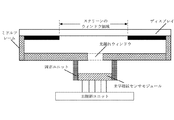
- 固定ユニットをさらに備え、前記ディスプレイの下方にミドルフレームが接続され、前記ミドルフレームの前記ディスプレイ内の前記指紋収集領域に対応する箇所に光漏れウィンドウが設置され、前記固定ユニットは記ミドルフレームと前記光学指紋センサモジュールとの間に接続され、前記光学指紋センサモジュールを前記ミドルフレームの前記光漏れウィンドウの下方に固定することを特徴とする請求項1〜16のいずれか一項に記載の指紋認識装置。
- ディスプレイと、
請求項1〜18のいずれか一項に記載の指紋認識装置と、を備えることを特徴とする電子機器。 - 前記ディスプレイは液晶ディスプレイLCDであることを特徴とする請求項19に記載の電子機器。
- 前記ディスプレイは有機発光ダイオードOLEDディスプレイであり、前記ディスプレイの発光層は複数の有機発光ダイオード光源を備え、前記指紋認識装置は少なくとも一部の有機発光ダイオード光源を指紋認識の励起光源とすることを特徴とする請求項19に記載の電子機器。
Applications Claiming Priority (1)
| Application Number | Priority Date | Filing Date | Title |
|---|---|---|---|
| PCT/CN2018/107115 WO2020056771A1 (zh) | 2018-09-21 | 2018-09-21 | 指纹识别装置和电子设备 |
Publications (2)
| Publication Number | Publication Date |
|---|---|
| JP2021508100A JP2021508100A (ja) | 2021-02-25 |
| JP6864120B2 true JP6864120B2 (ja) | 2021-04-21 |
Family
ID=65462475
Family Applications (1)
| Application Number | Title | Priority Date | Filing Date |
|---|---|---|---|
| JP2019561844A Active JP6864120B2 (ja) | 2018-09-21 | 2018-09-21 | 指紋認識装置及び電子機器 |
Country Status (5)
| Country | Link |
|---|---|
| US (1) | US20200097699A1 (ja) |
| EP (1) | EP3647995A1 (ja) |
| JP (1) | JP6864120B2 (ja) |
| CN (1) | CN109416737A (ja) |
| WO (1) | WO2020056771A1 (ja) |
Families Citing this family (43)
| Publication number | Priority date | Publication date | Assignee | Title |
|---|---|---|---|---|
| CN108885697B (zh) * | 2018-06-15 | 2021-11-05 | 深圳市汇顶科技股份有限公司 | 屏下生物特征识别装置和电子设备 |
| WO2020061748A1 (zh) * | 2018-09-25 | 2020-04-02 | 深圳市汇顶科技股份有限公司 | 光学图像采集装置和电子设备 |
| CN111310527A (zh) * | 2018-12-12 | 2020-06-19 | 上海耕岩智能科技有限公司 | 一种屏下图像获取结构及电子设备 |
| CN111725185A (zh) * | 2019-03-04 | 2020-09-29 | 苏州多感科技有限公司 | 图像传感器及其制备方法、图像识别方法、电子设备 |
| TWI732186B (zh) * | 2019-03-08 | 2021-07-01 | 聚積科技股份有限公司 | 屏下式感測顯示裝置 |
| CN109902652A (zh) * | 2019-03-11 | 2019-06-18 | 深圳阜时科技有限公司 | 生物特征检测模组和背光模组及电子装置 |
| CN109934157A (zh) * | 2019-03-11 | 2019-06-25 | 深圳阜时科技有限公司 | 一种背光模组、显示装置以及电子设备 |
| CN110088768B (zh) | 2019-03-12 | 2022-03-01 | 深圳市汇顶科技股份有限公司 | 屏下指纹识别装置和电子设备 |
| CN110062931B (zh) * | 2019-03-12 | 2021-07-16 | 深圳市汇顶科技股份有限公司 | 指纹识别装置、指纹识别方法和电子设备 |
| CN109815941A (zh) * | 2019-03-13 | 2019-05-28 | 上海思立微电子科技有限公司 | 指纹识别装置以及电子设备 |
| CN111695382B (zh) * | 2019-03-14 | 2024-02-13 | 北京小米移动软件有限公司 | 指纹采集区域确定方法和指纹采集区域确定装置 |
| EP3739508B1 (en) * | 2019-03-21 | 2022-02-16 | Shenzhen Goodix Technology Co., Ltd. | Fingerprint identification apparatus and electronic device |
| WO2020191596A1 (zh) * | 2019-03-25 | 2020-10-01 | 深圳市汇顶科技股份有限公司 | 指纹识别装置和电子设备 |
| CN110741381A (zh) * | 2019-03-25 | 2020-01-31 | 深圳市汇顶科技股份有限公司 | 指纹识别装置和电子设备 |
| CN208848221U (zh) | 2019-04-10 | 2019-05-10 | 深圳市汇顶科技股份有限公司 | 光学指纹识别装置和电子设备 |
| CN111832359A (zh) * | 2019-04-19 | 2020-10-27 | 格科微电子(上海)有限公司 | 降低光学指纹识别模组高度的方法 |
| WO2020215187A1 (zh) * | 2019-04-22 | 2020-10-29 | 深圳市汇顶科技股份有限公司 | 指纹识别的装置和电子设备 |
| CN110071994A (zh) * | 2019-04-25 | 2019-07-30 | Oppo广东移动通信有限公司 | 电子设备 |
| WO2020220219A1 (zh) * | 2019-04-29 | 2020-11-05 | 深圳市汇顶科技股份有限公司 | 生物特征识别装置、方法和电子设备 |
| CN111914593A (zh) * | 2019-05-08 | 2020-11-10 | 上海耕岩智能科技有限公司 | 图像采集方法及装置、存储介质、电子设备 |
| CN110291531B (zh) * | 2019-05-15 | 2023-06-16 | 深圳市汇顶科技股份有限公司 | 指纹识别的方法、装置和电子设备 |
| CN110110701B (zh) * | 2019-05-21 | 2024-05-14 | 深圳市隆利科技股份有限公司 | 一种指纹识别模组 |
| CN111164609B (zh) * | 2019-06-14 | 2023-10-13 | 深圳市汇顶科技股份有限公司 | 指纹识别装置和电子设备 |
| CN110741383B (zh) * | 2019-06-14 | 2021-08-06 | 深圳市汇顶科技股份有限公司 | 光学指纹装置和电子设备 |
| CN110321832B (zh) * | 2019-06-28 | 2021-05-18 | 维沃移动通信有限公司 | 光学模组及移动终端 |
| CN112418201A (zh) * | 2019-08-22 | 2021-02-26 | 京东方科技集团股份有限公司 | 指纹识别模组及其驱动方法和显示装置 |
| EP3812955B1 (en) | 2019-08-28 | 2022-07-06 | Shenzhen Goodix Technology Co., Ltd. | Fingerprint detection apparatus and electronic device |
| CN211062054U (zh) * | 2019-08-30 | 2020-07-21 | 指纹卡有限公司 | 生物特征成像布置和电子装置 |
| WO2021042396A1 (zh) * | 2019-09-06 | 2021-03-11 | 深圳市汇顶科技股份有限公司 | 指纹识别装置和电子设备 |
| CN110738193B (zh) * | 2019-10-31 | 2024-01-12 | 维沃移动通信有限公司 | 电子设备 |
| CN111052139B (zh) * | 2019-11-05 | 2024-03-15 | 深圳市汇顶科技股份有限公司 | 屏下指纹识别装置、lcd指纹识别系统和电子设备 |
| CN111339835A (zh) * | 2020-02-06 | 2020-06-26 | 京东方科技集团股份有限公司 | 屏下指纹识别显示模组、显示装置和电子设备 |
| CN111507273B (zh) * | 2020-04-20 | 2024-02-02 | 京东方科技集团股份有限公司 | 显示面板、显示装置和显示面板的制作方法 |
| CN111554009B (zh) * | 2020-04-23 | 2022-01-11 | 赣州深奥科技有限公司 | 一种指纹头结构 |
| CN111753637A (zh) * | 2020-04-30 | 2020-10-09 | 深圳市汇顶科技股份有限公司 | 一种指纹识别装置及移动电子设备 |
| CN111708405A (zh) * | 2020-06-22 | 2020-09-25 | Oppo广东移动通信有限公司 | 指纹识别组件以及穿戴设备 |
| CN111860296B (zh) * | 2020-07-17 | 2024-04-09 | 敦泰电子(深圳)有限公司 | 一种光学指纹识别模组、显示模组及其指纹识别方法 |
| CN116529789A (zh) * | 2020-10-30 | 2023-08-01 | 谷歌有限责任公司 | 使用用户触摸与指纹传感器的搭配进行指纹注册 |
| CN112464799A (zh) * | 2020-11-25 | 2021-03-09 | 京东方科技集团股份有限公司 | 指纹识别基板及其制备方法、识别方法和显示装置 |
| CN112486352B (zh) * | 2020-11-27 | 2022-07-12 | Tcl华星光电技术有限公司 | 触控显示面板 |
| WO2022165770A1 (zh) * | 2021-02-05 | 2022-08-11 | 深圳市汇顶科技股份有限公司 | 芯片封装结构和电子设备 |
| TWI777742B (zh) * | 2021-05-18 | 2022-09-11 | 友達光電股份有限公司 | 指紋辨識裝置 |
| JPWO2023085148A1 (ja) * | 2021-11-12 | 2023-05-19 |
Family Cites Families (13)
| Publication number | Priority date | Publication date | Assignee | Title |
|---|---|---|---|---|
| CN101672995B (zh) * | 2009-09-29 | 2011-04-06 | 友达光电股份有限公司 | 感测方法 |
| CN106570442B (zh) * | 2015-10-09 | 2021-05-14 | 小米科技有限责任公司 | 指纹识别方法及装置 |
| US10635878B2 (en) * | 2015-10-23 | 2020-04-28 | Shenzhen GOODIX Technology Co., Ltd. | Optical fingerprint sensor with force sensing capability |
| US10268884B2 (en) * | 2016-01-29 | 2019-04-23 | Synaptics Incorporated | Optical fingerprint sensor under a display |
| CN106815573B (zh) * | 2017-01-06 | 2019-11-19 | 武汉华星光电技术有限公司 | 显示屏及电子装置 |
| CN106991387A (zh) * | 2017-03-23 | 2017-07-28 | 宇龙计算机通信科技(深圳)有限公司 | 一种全屏指纹采集方法及移动终端 |
| CN107195675B (zh) * | 2017-04-27 | 2019-09-27 | Oppo广东移动通信有限公司 | 显示屏、显示装置及移动终端 |
| CN107194224B (zh) * | 2017-04-28 | 2020-09-22 | Oppo广东移动通信有限公司 | 解锁控制方法及相关产品 |
| WO2019061535A1 (zh) * | 2017-09-30 | 2019-04-04 | 深圳市汇顶科技股份有限公司 | 指纹识别的方法、装置和终端设备 |
| CN207557977U (zh) * | 2017-12-05 | 2018-06-29 | 深圳市为通博科技有限责任公司 | 光路调制器、指纹识别装置和终端设备 |
| CN108171037A (zh) * | 2017-12-27 | 2018-06-15 | 努比亚技术有限公司 | 应用启动方法、终端和计算机存储介质 |
| CN108235750B (zh) * | 2018-01-15 | 2021-06-11 | 深圳市汇顶科技股份有限公司 | 指纹识别系统的按压检测方法、装置和终端设备 |
| CN108513666B (zh) * | 2018-03-22 | 2022-05-17 | 深圳市汇顶科技股份有限公司 | 屏下生物特征识别装置和电子设备 |
-
2018
- 2018-09-21 JP JP2019561844A patent/JP6864120B2/ja active Active
- 2018-09-21 EP EP18907464.4A patent/EP3647995A1/en not_active Ceased
- 2018-09-21 WO PCT/CN2018/107115 patent/WO2020056771A1/zh unknown
- 2018-09-21 CN CN201880001566.2A patent/CN109416737A/zh active Pending
-
2019
- 2019-08-27 US US16/551,715 patent/US20200097699A1/en not_active Abandoned
Also Published As
| Publication number | Publication date |
|---|---|
| CN109416737A (zh) | 2019-03-01 |
| US20200097699A1 (en) | 2020-03-26 |
| JP2021508100A (ja) | 2021-02-25 |
| EP3647995A4 (en) | 2020-05-06 |
| WO2020056771A1 (zh) | 2020-03-26 |
| EP3647995A1 (en) | 2020-05-06 |
Similar Documents
| Publication | Publication Date | Title |
|---|---|---|
| JP6864120B2 (ja) | 指紋認識装置及び電子機器 | |
| CN209962265U (zh) | 指纹识别装置和电子设备 | |
| US11048903B2 (en) | Under-LCD screen optical sensor module for on-screen fingerprint sensing | |
| US10331939B2 (en) | Multi-layer optical designs of under-screen optical sensor module having spaced optical collimator array and optical sensor array for on-screen fingerprint sensing | |
| US10318791B2 (en) | Anti-spoofing sensing for rejecting fake fingerprint patterns in under-screen optical sensor module for on-screen fingerprint sensing | |
| CN109496313B (zh) | 指纹识别装置和电子设备 | |
| US11030434B2 (en) | Lens-pinhole array designs in ultra thin under screen optical sensors for on-screen fingerprint sensing | |
| EP3465399B1 (en) | Optical collimators for under-screen optical sensor module for on-screen fingerprint sensing | |
| US10614283B2 (en) | Devices with peripheral task bar display zone and under-LCD screen optical sensor module for on-screen fingerprint sensing | |
| CN109791599B (zh) | 用于屏幕上指纹感应的屏幕下光学传感器模块 | |
| US10410037B2 (en) | Under-screen optical sensor module for on-screen fingerprint sensing implementing imaging lens, extra illumination or optical collimator array | |
| EP3254235B1 (en) | Under-screen optical sensor module for on-screen fingerprint sensing | |
| CN109791325B (zh) | 具有外围任务栏显示区的设备和用于屏上指纹感测的lcd屏下光学传感器模块 | |
| CN109196525B (zh) | 在用于屏上指纹感测的屏下光学传感器模块中拒绝假指纹图案的反欺骗感测 | |
| WO2020077506A1 (zh) | 指纹识别方法、装置及具有指纹识别功能的终端设备 | |
| US11210491B2 (en) | Fingerprint sensor under a display module with tilted receiving optics | |
| KR102374723B1 (ko) | 광학 지문 장치 및 전자 기기 | |
| WO2020093251A1 (zh) | 基于双感应区的识别指纹方法、指纹识别系统和电子设备 | |
| WO2020082375A1 (zh) | 复合透镜结构、指纹识别装置和电子设备 | |
| WO2020168495A1 (zh) | 用于指纹识别的方法、装置和终端设备 | |
| CN110770750B (zh) | 指纹识别的装置和电子设备 | |
| WO2020168496A1 (zh) | 用于指纹识别的方法、装置和终端设备 | |
| CN210534801U (zh) | 指纹识别装置和电子设备 | |
| CN111183429B (zh) | 指纹识别的方法、装置和电子设备 | |
| WO2020073166A1 (zh) | 指纹识别方法、装置和终端设备 |
Legal Events
| Date | Code | Title | Description |
|---|---|---|---|
| A521 | Request for written amendment filed |
Free format text: JAPANESE INTERMEDIATE CODE: A523 Effective date: 20191108 |
|
| A621 | Written request for application examination |
Free format text: JAPANESE INTERMEDIATE CODE: A621 Effective date: 20191108 |
|
| A871 | Explanation of circumstances concerning accelerated examination |
Free format text: JAPANESE INTERMEDIATE CODE: A871 Effective date: 20191108 |
|
| A975 | Report on accelerated examination |
Free format text: JAPANESE INTERMEDIATE CODE: A971005 Effective date: 20201014 |
|
| A131 | Notification of reasons for refusal |
Free format text: JAPANESE INTERMEDIATE CODE: A131 Effective date: 20201020 |
|
| A521 | Request for written amendment filed |
Free format text: JAPANESE INTERMEDIATE CODE: A523 Effective date: 20201218 |
|
| A131 | Notification of reasons for refusal |
Free format text: JAPANESE INTERMEDIATE CODE: A131 Effective date: 20210112 |
|
| A521 | Request for written amendment filed |
Free format text: JAPANESE INTERMEDIATE CODE: A523 Effective date: 20210312 |
|
| TRDD | Decision of grant or rejection written | ||
| A01 | Written decision to grant a patent or to grant a registration (utility model) |
Free format text: JAPANESE INTERMEDIATE CODE: A01 Effective date: 20210323 |
|
| A61 | First payment of annual fees (during grant procedure) |
Free format text: JAPANESE INTERMEDIATE CODE: A61 Effective date: 20210401 |
|
| R150 | Certificate of patent or registration of utility model |
Ref document number: 6864120 Country of ref document: JP Free format text: JAPANESE INTERMEDIATE CODE: R150 |
|
| R250 | Receipt of annual fees |
Free format text: JAPANESE INTERMEDIATE CODE: R250 |