JP6864120B2 - Fingerprint recognition device and electronic equipment - Google Patents
Fingerprint recognition device and electronic equipment Download PDFInfo
- Publication number
- JP6864120B2 JP6864120B2 JP2019561844A JP2019561844A JP6864120B2 JP 6864120 B2 JP6864120 B2 JP 6864120B2 JP 2019561844 A JP2019561844 A JP 2019561844A JP 2019561844 A JP2019561844 A JP 2019561844A JP 6864120 B2 JP6864120 B2 JP 6864120B2
- Authority
- JP
- Japan
- Prior art keywords
- fingerprint
- optical
- display
- fingerprint recognition
- sensor
- Prior art date
- Legal status (The legal status is an assumption and is not a legal conclusion. Google has not performed a legal analysis and makes no representation as to the accuracy of the status listed.)
- Active
Links
- 230000003287 optical effect Effects 0.000 claims description 242
- 238000001514 detection method Methods 0.000 claims description 74
- 238000001914 filtration Methods 0.000 claims description 36
- 238000003491 array Methods 0.000 claims description 13
- 238000012360 testing method Methods 0.000 claims description 10
- 239000004973 liquid crystal related substance Substances 0.000 claims description 9
- 230000005284 excitation Effects 0.000 claims description 7
- 238000010586 diagram Methods 0.000 description 13
- 238000000034 method Methods 0.000 description 13
- 238000005516 engineering process Methods 0.000 description 8
- 238000003384 imaging method Methods 0.000 description 8
- 238000003825 pressing Methods 0.000 description 8
- 230000006870 function Effects 0.000 description 6
- 238000013461 design Methods 0.000 description 5
- 230000005540 biological transmission Effects 0.000 description 4
- 238000009826 distribution Methods 0.000 description 4
- 239000010410 layer Substances 0.000 description 4
- 239000004065 semiconductor Substances 0.000 description 4
- 230000008878 coupling Effects 0.000 description 3
- 238000010168 coupling process Methods 0.000 description 3
- 238000005859 coupling reaction Methods 0.000 description 3
- 238000005304 joining Methods 0.000 description 3
- 238000012634 optical imaging Methods 0.000 description 3
- 238000012545 processing Methods 0.000 description 3
- 230000001681 protective effect Effects 0.000 description 3
- 238000003860 storage Methods 0.000 description 3
- 229910052581 Si3N4 Inorganic materials 0.000 description 2
- VYPSYNLAJGMNEJ-UHFFFAOYSA-N Silicium dioxide Chemical compound O=[Si]=O VYPSYNLAJGMNEJ-UHFFFAOYSA-N 0.000 description 2
- 239000008280 blood Substances 0.000 description 2
- 210000004369 blood Anatomy 0.000 description 2
- 238000000576 coating method Methods 0.000 description 2
- 238000004891 communication Methods 0.000 description 2
- 230000000694 effects Effects 0.000 description 2
- 230000001788 irregular Effects 0.000 description 2
- 239000011241 protective layer Substances 0.000 description 2
- HQVNEWCFYHHQES-UHFFFAOYSA-N silicon nitride Chemical compound N12[Si]34N5[Si]62N3[Si]51N64 HQVNEWCFYHHQES-UHFFFAOYSA-N 0.000 description 2
- 229910052814 silicon oxide Inorganic materials 0.000 description 2
- WQZGKKKJIJFFOK-GASJEMHNSA-N Glucose Natural products OC[C@H]1OC(O)[C@H](O)[C@@H](O)[C@@H]1O WQZGKKKJIJFFOK-GASJEMHNSA-N 0.000 description 1
- QVGXLLKOCUKJST-UHFFFAOYSA-N atomic oxygen Chemical compound [O] QVGXLLKOCUKJST-UHFFFAOYSA-N 0.000 description 1
- 230000000903 blocking effect Effects 0.000 description 1
- 230000017531 blood circulation Effects 0.000 description 1
- 238000011161 development Methods 0.000 description 1
- 230000009977 dual effect Effects 0.000 description 1
- 230000002708 enhancing effect Effects 0.000 description 1
- 239000010408 film Substances 0.000 description 1
- 239000011521 glass Substances 0.000 description 1
- 239000008103 glucose Substances 0.000 description 1
- 230000002452 interceptive effect Effects 0.000 description 1
- 239000000463 material Substances 0.000 description 1
- 239000013307 optical fiber Substances 0.000 description 1
- 239000012788 optical film Substances 0.000 description 1
- 229910052760 oxygen Inorganic materials 0.000 description 1
- 239000001301 oxygen Substances 0.000 description 1
- 230000002093 peripheral effect Effects 0.000 description 1
- 230000001902 propagating effect Effects 0.000 description 1
- 229910052594 sapphire Inorganic materials 0.000 description 1
- 239000010980 sapphire Substances 0.000 description 1
- 238000000926 separation method Methods 0.000 description 1
- 230000008054 signal transmission Effects 0.000 description 1
- 238000006467 substitution reaction Methods 0.000 description 1
- 239000000758 substrate Substances 0.000 description 1
- 238000012795 verification Methods 0.000 description 1
- 230000000007 visual effect Effects 0.000 description 1
Images


Classifications
-
- G—PHYSICS
- G06—COMPUTING; CALCULATING OR COUNTING
- G06V—IMAGE OR VIDEO RECOGNITION OR UNDERSTANDING
- G06V40/00—Recognition of biometric, human-related or animal-related patterns in image or video data
- G06V40/10—Human or animal bodies, e.g. vehicle occupants or pedestrians; Body parts, e.g. hands
- G06V40/12—Fingerprints or palmprints
- G06V40/13—Sensors therefor
- G06V40/1318—Sensors therefor using electro-optical elements or layers, e.g. electroluminescent sensing
-
- H—ELECTRICITY
- H10—SEMICONDUCTOR DEVICES; ELECTRIC SOLID-STATE DEVICES NOT OTHERWISE PROVIDED FOR
- H10K—ORGANIC ELECTRIC SOLID-STATE DEVICES
- H10K50/00—Organic light-emitting devices
- H10K50/80—Constructional details
- H10K50/86—Arrangements for improving contrast, e.g. preventing reflection of ambient light
-
- H—ELECTRICITY
- H10—SEMICONDUCTOR DEVICES; ELECTRIC SOLID-STATE DEVICES NOT OTHERWISE PROVIDED FOR
- H10K—ORGANIC ELECTRIC SOLID-STATE DEVICES
- H10K59/00—Integrated devices, or assemblies of multiple devices, comprising at least one organic light-emitting element covered by group H10K50/00
- H10K59/80—Constructional details
- H10K59/8791—Arrangements for improving contrast, e.g. preventing reflection of ambient light
-
- G—PHYSICS
- G06—COMPUTING; CALCULATING OR COUNTING
- G06V—IMAGE OR VIDEO RECOGNITION OR UNDERSTANDING
- G06V40/00—Recognition of biometric, human-related or animal-related patterns in image or video data
- G06V40/10—Human or animal bodies, e.g. vehicle occupants or pedestrians; Body parts, e.g. hands
- G06V40/12—Fingerprints or palmprints
- G06V40/1341—Sensing with light passing through the finger
-
- H—ELECTRICITY
- H10—SEMICONDUCTOR DEVICES; ELECTRIC SOLID-STATE DEVICES NOT OTHERWISE PROVIDED FOR
- H10K—ORGANIC ELECTRIC SOLID-STATE DEVICES
- H10K59/00—Integrated devices, or assemblies of multiple devices, comprising at least one organic light-emitting element covered by group H10K50/00
- H10K59/60—OLEDs integrated with inorganic light-sensitive elements, e.g. with inorganic solar cells or inorganic photodiodes
- H10K59/65—OLEDs integrated with inorganic image sensors
Description
本発明は、指紋認識の技術分野に関し、より具体的には、指紋認識装置及び電子機器に関する。 The present invention relates to the technical field of fingerprint recognition, and more specifically to a fingerprint recognition device and an electronic device.
携帯電話産業の急速発展に伴って、指紋認識技術はますます注目されており、アンダーディスプレイ指紋認識技術の実用化は望まれている。光学アンダーディスプレイ指紋認識技術とは、光源の発する光が指に反射されて形成された反射光を指紋センサによって収集し、反射光に指の指紋情報を持たせることによって、アンダーディスプレイ指紋認識を実現することである。指紋認識時、ディスプレイには特定のガイドアイコンが指紋センサの配置位置に対応して表示され、ユーザーは指を該ガイドアイコンの表示位置に置いて指紋認識を行う必要があるため、ユーザーエクスペリエンスが悪い。 With the rapid development of the mobile phone industry, fingerprint recognition technology is attracting more and more attention, and practical application of under-display fingerprint recognition technology is desired. Optical under-display fingerprint recognition technology realizes under-display fingerprint recognition by collecting the reflected light formed by reflecting the light emitted by the light source on the finger with a fingerprint sensor and giving the reflected light the fingerprint information of the finger. It is to be. At the time of fingerprint recognition, a specific guide icon is displayed on the display corresponding to the position of the fingerprint sensor, and the user needs to place a finger at the display position of the guide icon to perform fingerprint recognition, resulting in a poor user experience. ..
本願の実施例は、指紋認識時のユーザーエクスペリエンスを向上させるとともに、指紋認識のセキュリティを向上させることができる指紋認識装置及び電子機器を提供する。 An embodiment of the present application provides a fingerprint recognition device and an electronic device capable of improving the user experience at the time of fingerprint recognition and improving the security of fingerprint recognition.
第1態様では、ディスプレイを備えた電子機器に応用され、指紋収集領域の少なくとも一部が前記ディスプレイの表示領域内に位置するようにディスプレイの下方に設置される光学指紋センサモジュールを備え、前記光学指紋センサモジュールは複数のセンサダイを備え、前記複数のセンサダイの検出領域がそれぞれ前記指紋収集領域の複数のサブ領域に対応し、各センサダイは対応するサブ領域の上方からの光信号を検出する、指紋認識装置を提供する。 In the first aspect, the optical fingerprint sensor module is applied to an electronic device including a display and is installed below the display so that at least a part of the fingerprint collection area is located in the display area of the display. The fingerprint sensor module includes a plurality of sensor dies, each of the detection regions of the plurality of sensor dies corresponds to a plurality of sub-regions of the fingerprint collection region, and each sensor die detects an optical signal from above the corresponding sub-region. Provide a recognition device.
1つの可能な実施形態では、被験指が前記複数のサブ領域のうち一部のサブ領域の上方に位置する時、前記一部のサブ領域に対応するセンサダイが動作状態にある。 In one possible embodiment, when the test finger is located above some of the plurality of sub-regions, the sensor die corresponding to the portion of the sub-regions is in the operating state.
1つの可能な実施形態では、被験指が前記複数のサブ領域のうち一部のサブ領域の上方に位置する時、前記複数のセンサダイがいずれも動作状態にある。 In one possible embodiment, the plurality of sensor dies are all in operation when the test finger is located above some of the plurality of sub-regions.
1つの可能な実施形態では、前記複数のサブ領域がディスプレイの両側に分布し、又は前記複数のサブ領域が前記ディスプレイの同一側に分布し、又は前記複数のサブ領域が前記ディスプレイの中間領域に分布する。 In one possible embodiment, the plurality of sub-regions are distributed on both sides of the display, or the plurality of sub-regions are distributed on the same side of the display, or the plurality of sub-regions are distributed in an intermediate region of the display. To be distributed.
前記複数のサブ領域はディスプレイの離散的又は連続的な任意の位置に分布してもよく、異なる電子機器の使用ニーズを満たすようにクライアントのニーズに応じてカスタマイズしてもよい。 The plurality of sub-regions may be distributed at arbitrary positions discretely or continuously on the display, or may be customized according to the needs of the client to meet the usage needs of different electronic devices.
1つの可能な実施形態では、前記複数のサブ領域のサイズは同じであり、又は前記複数のサブ領域のサイズはすべて同じではない。 In one possible embodiment, the sizes of the plurality of sub-regions are the same, or the sizes of the plurality of sub-regions are not all the same.
1つの可能な実施形態では、前記指紋認識装置は、それぞれ前記複数のセンサダイに対応する複数の光路変調器をさらに備え、各光路変調器は光信号を対応するセンサダイの光検出アレイにガイドする。 In one possible embodiment, the fingerprint recognizer further comprises a plurality of optical path modulators, each corresponding to the plurality of sensor dies, each optical path modulator guiding an optical signal to an optical detection array of the corresponding sensor dies.
1つの可能な実施形態では、前記指紋認識装置は少なくとも1つの共通光路変調器をさらに備え、各共通光路変調器は少なくとも1つのセンサダイに対応し、光信号をそれぞれ対応するセンサダイの光検出アレイにガイドする。 In one possible embodiment, the fingerprint recognizer further comprises at least one common optical path modulator, each common optical path modulator corresponding to at least one sensor die, each optical signal in a corresponding sensor die light detection array. Guide.
1つの可能な実施形態では、前記光路変調器は、光路コリメータ、集束レンズ及びマイクロレンズアレイのうちの少なくとも1種を備える。 In one possible embodiment, the optical path modulator comprises at least one of an optical path collimator, a focusing lens and a microlens array.
1つの可能な実施形態では、前記光路変調器は対応するセンサダイと一体にパッケージされ、又は、前記光路変調器は前記光学指紋センサモジュールとは独立した部材として前記指紋認識装置の内部に取り付けられる。 In one possible embodiment, the optical path modulator is packaged integrally with the corresponding sensor die, or the optical path modulator is mounted inside the fingerprint recognition device as a member independent of the optical fingerprint sensor module.
1つの可能な実施形態では、前記指紋認識装置は、それぞれ前記複数のセンサダイに対応する複数のフィルタリングユニットをさらに備え、各フィルタリングユニットは対応するセンサダイに伝送される光信号の波長を選択する。 In one possible embodiment, the fingerprint recognition device further comprises a plurality of filtering units, each corresponding to the plurality of sensor dies, each filtering unit selecting the wavelength of an optical signal transmitted to the corresponding sensor dies.
1つの可能な実施形態では、前記指紋認識装置は少なくとも1つの共通フィルタリングユニットをさらに備え、各共通フィルタリングユニットは少なくとも1つのセンサダイに対応し、対応するセンサダイに伝送される光信号の波長を選択する。 In one possible embodiment, the fingerprint recognition device further comprises at least one common filtering unit, each common filtering unit corresponding to at least one sensor die and selecting the wavelength of the optical signal transmitted to the corresponding sensor die. ..
1つの可能な実施形態では、前記フィルタリングユニットによって選択される光信号の波長は可視光波長又は近赤外光波長を含む。 In one possible embodiment, the wavelength of the optical signal selected by the filtering unit includes visible or near infrared wavelengths.
1つの可能な実施形態では、前記フィルタリングユニットは対応するセンサダイと一体にパッケージされ(たとえば、コーティングの方式によってセンサダイと一体にパッケージされ)、又は、前記フィルタリングユニットは対応するセンサダイの上方の光路変調器と一体にパッケージされ、又は、前記フィルタリングユニットは対応するセンサダイ及び光路変調器と一体にパッケージされ、又は、前記フィルタリングユニットは前記光学指紋センサモジュール及び光路変調器とは独立した部材として前記指紋認識装置の内部に取り付けられる。 In one possible embodiment, the filtering unit is packaged integrally with the corresponding sensor die (eg, packaged integrally with the sensor die by a coating method), or the filtering unit is an optical path modulator above the corresponding sensor die. The filtering unit is packaged integrally with the corresponding sensor die and the optical path modulator, or the filtering unit is the fingerprint recognition device as a member independent of the optical fingerprint sensor module and the optical path modulator. It is installed inside the.
1つの可能な実施形態では、前記指紋認識装置は、それぞれ前記複数のセンサダイに対応する複数の制御ユニットをさらに備え、各制御ユニットは光信号検出を行うように対応するセンサダイの光検出アレイを制御する。 In one possible embodiment, the fingerprint recognition device further comprises a plurality of control units corresponding to the plurality of sensor dies, each of which controls an optical detection array of the corresponding sensor dies to perform optical signal detection. To do.
該制御ユニットはさらに、該指紋認識装置を用いた装置の主制御ユニットからのコマンド及び伝送データに応答できる。 The control unit can further respond to commands and transmission data from the main control unit of the device using the fingerprint recognition device.
1つの可能な実施形態では、前記指紋認識装置は、光信号検出を行うように前記複数のセンサダイの光検出アレイを制御する共通制御ユニットをさらに備える。
該共通制御ユニットはさらに、該指紋認識装置を用いた装置の主制御ユニットからのコマンド及び伝送データに応答できる。
In one possible embodiment, the fingerprint recognition device further comprises a common control unit that controls the photodetection arrays of the plurality of sensor dies to perform optical signal detection.
The common control unit can further respond to commands and transmission data from the main control unit of the device using the fingerprint recognition device.
1つの可能な実施形態では、前記指紋認識装置は制御ユニットを備えず、前記指紋認識装置を用いた装置の主制御ユニットは光信号検出を行うように前記複数のセンサダイの光検出アレイを制御する。 In one possible embodiment, the fingerprint recognition device does not include a control unit, and the main control unit of the device using the fingerprint recognition device controls the photodetection array of the plurality of sensor dies so as to perform optical signal detection. ..
1つの可能な実施形態では、前記指紋認識装置は、ディスプレイと前記光学指紋センサモジュールとの間に接続され、前記光学指紋センサモジュールをディスプレイ内の前記指紋収集領域の下方に固定する固定ユニットをさらに備える。 In one possible embodiment, the fingerprint recognition device further comprises a fixation unit that is connected between the display and the optical fingerprint sensor module to secure the optical fingerprint sensor module below the fingerprint collection area in the display. Be prepared.
1つの可能な実施形態では、前記指紋認識装置は固定ユニットをさらに備え、ディスプレイの下方にミドルフレームが接続され、前記ミドルフレームの前記ディスプレイ内の前記指紋収集領域に対応する箇所に光漏れウィンドウが設置され、前記固定ユニットは記ミドルフレームと前記光学指紋センサモジュールとの間に接続され、前記光学指紋センサモジュールを前記ミドルフレームの前記光漏れウィンドウの下方に固定する。 In one possible embodiment, the fingerprint recognition device further comprises a fixed unit, a middle frame is connected below the display, and a light leak window is located in the middle frame in the display corresponding to the fingerprint collection area. Installed, the fixing unit is connected between the writing middle frame and the optical fingerprint sensor module to secure the optical fingerprint sensor module below the light leak window of the middle frame.
第2態様では、ディスプレイ、及び第1態様又は第1態様の可能な実施形態のいずれかに記載の指紋認識装置を備える、電子機器を提供する。
1つの可能な実施形態では、前記ディスプレイは液晶ディスプレイ(LCDディスプレイ)である。
A second aspect provides an electronic device comprising a display and a fingerprint recognition device according to either the first aspect or the possible embodiment of the first aspect.
In one possible embodiment, the display is a liquid crystal display (LCD display).
1つの可能な実施形態では、前記ディスプレイは有機発光ダイオードOLEDディスプレイであり、前記ディスプレイの発光層は複数の有機発光ダイオード光源を備え、前記指紋認識装置は少なくとも一部の有機発光ダイオード光源を指紋認識の励起光源とする。 In one possible embodiment, the display is an organic light emitting OLED display, the light emitting layer of the display comprises a plurality of organic light emitting diode light sources, and the fingerprint recognition device fingerprint-recognizes at least a part of the organic light emitting diode light sources. It is used as an excitation light source of.
上記技術案によれば、該指紋認識装置の光学指紋センサモジュールが複数のセンサダイを備えることで、ディスプレイの指紋収集領域の面積を増加させ、ユーザーの被験指の大きな移動範囲を許容し、指紋認識時のユーザーエクスペリエンスを向上させる。また、複数のセンサダイが一体に接合される場合、指のより大きな面積の指紋情報を収集でき、又はより多くの指の指紋情報を同時に収集でき、指紋パスワードの長さを増加することに相当し、指紋認識のセキュリティを向上させる。また、ユーザーはより多くの有効指紋特徴を提供できることで、さらに本人拒否率(False Rejection Rate、FRR)と他人受入率(False Acceptance Rate、FAR)を低減させ、指紋ロック解除の正確率を高め、更にユーザーエクスペリエンスを向上させる。 According to the above technical proposal, the optical fingerprint sensor module of the fingerprint recognition device includes a plurality of sensor dies to increase the area of the fingerprint collection area of the display, allow a large movement range of the user's test finger, and perform fingerprint recognition. Improve the user experience of the time. Also, when multiple sensor dies are joined together, it is possible to collect fingerprint information on a larger area of the finger, or collect fingerprint information on more fingers at the same time, which corresponds to increasing the length of the fingerprint password. , Improve the security of fingerprint recognition. In addition, users can provide more valid fingerprint features, further reducing false rejection rate (FRR) and false acceptance rate (FAR), and increasing the accuracy rate of fingerprint unlocking. Further improve the user experience.
以下、図面を参照して本願の実施例の技術案を説明する。 Hereinafter, the technical proposal of the embodiment of the present application will be described with reference to the drawings.
電子機器がフルスクリーンの時代に突入するに伴って、電子機器の前面の指紋収集領域がフルスクリーンに絞られているため、アンダーディスプレイ(Under−display又はUnder−screen)指紋認識技術はますます注目される。アンダーディスプレイ指紋認識技術とは、指紋認識モジュールをディスプレイの下方に取り付けることで、ディスプレイの表示領域内での指紋認識操作を実現することであり、電子機器の前面の表示領域以外の領域に指紋収集領域を設置せずに済む。 Underdisplay (Under-display or Under-screen) fingerprint recognition technology is gaining more and more attention as electronic devices enter the full-screen era and the fingerprint collection area on the front of the electronic device is narrowed down to full screen. Will be done. The under display fingerprint recognition technology, by attaching the fingerprint recognition module below the display, is to realize a fingerprint recognition operation within the display area of the display, the fingerprint in an area other than the display area of the front surface of the electronic device There is no need to set up a collection area.
光学アンダーディスプレイ指紋認識技術は、装置表示ユニットの頂面から戻った光を用いて、指紋検出及びほかの検出操作を行う。該戻った光は該頂面に接触する物体(たとえば、指)の情報を含み、該戻った光を収集して検出することで、ディスプレイの下方に位置する特定の光学センサモジュールを実現する。光学センサモジュールは、戻った光を収集して検出するための光学素子を適切に配置することで、所望する光学イメージングを実現するように設計されてもよい。 Optical under-display fingerprint recognition technology uses the light returned from the top of the device display unit to perform fingerprint detection and other detection operations. The returned light contains information about an object (eg, a finger) in contact with the top surface, and by collecting and detecting the returned light, a specific optical sensor module located below the display is realized. The optical sensor module may be designed to achieve the desired optical imaging by properly arranging optical elements for collecting and detecting the returned light.
なお、本願の実施例の技術案は各種の電子機器、たとえばスマートフォン、ノートパソコン、タブレットPC、ゲーム装置等の携帯型又はモバイルコンピューティング装置、及び電子データベース、自動車、銀行現金自動預払機(Automated Teller
Machine、ATM)などのほかの電子機器に適用でき、本願の実施例ではそれを限定しない。
In addition, the technical proposal of the embodiment of the present application includes various electronic devices, for example, portable or mobile computing devices such as smartphones, notebook computers, tablet PCs, game devices, electronic databases, automobiles, and automated teller machines (Automated Tellers).
It can be applied to other electronic devices such as Machine, ATM), and the examples of the present application do not limit it.
図1及び図2は指紋認識装置を適用できる電子機器100の模式図であり、図1は電子機器100の正面模式図、図2は図1に示される電子機器100のA−A’線矢視部分断面構造模式図である。
1 and 2 are schematic views of the
図1及び図2に示すように、電子機器100はディスプレイ120と指紋認識モジュール140とを備え、前記ディスプレイ120は表示領域102を有し、前記指紋認識モジュール140は前記ディスプレイ120の下方に設置される。
As shown in FIGS. 1 and 2, the
前記ディスプレイ120は自発光型ディスプレイであってもよく、自発光性を有する表示ユニットを表示画素とする。たとえば、ディスプレイ120は有機発光ダイオード(Organic Light−Emitting Diode、OLED)ディスプレイ又はマイクロ発光ダイオード(Micro−LED)ディスプレイである。ほかの代替実施例では、前記ディスプレイ120は液晶ディスプレイ(Liquid Crystal Display、LCD)又はほかの受動発光型ディスプレイであり、本願の実施例ではそれを限定しない。
The
一方、前記ディスプレイ120は、たとえば、タッチディスプレイであり、画面表示を行うだけでなく、ユーザーのタッチ又は押圧操作を検出でき、それによりユーザーにマンマシンインタフェースを提供する。たとえば、一実施例では、前記電子機器100はタッチセンサを備え、前記タッチセンサは、具体的には、タッチパネル(Touch Panel、TP)であり、前記ディスプレイ120の表面に設置されてもよく、その一部又は全体が前記ディスプレイ120の内部に集積されて、前記タッチディスプレイを形成してもよい。
On the other hand, the
前記指紋認識モジュール140は、具体的には、光学指紋認識モジュールであり、主にユーザーの指紋情報(たとえば、指紋画像情報)を収集する。本願の実施例では、前記指紋認識モジュール140は少なくとも前記ディスプレイ120の下方の局所領域に設置され、それにより前記指紋認識モジュール140の指紋収集領域(又は検出領域)130の少なくとも一部を前記ディスプレイ120の表示領域102に位置させ、ここで、指紋収集領域130の面積は指紋認識モジュール140の面積と異なってもよく、たとえば、レンズイメージングの光路設計、反射式折畳み光路設計又はほかの光の収束又は反射等のような光路設計によって、前記指紋認識モジュール140の指紋収集領域130の面積を指紋認識モジュール140の面積よりも大きくする。ほかの代替実施形態では、たとえば光コリメーション方式によって光路ガイドを行う場合、前記指紋認識モジュール140の指紋収集領域130は前記指紋認識モジュール140の面積と同じになるようにしてもよい。
Specifically, the
一実施例として、前記指紋認識モジュール140は、具体的には、光検出アレイを有する複数の光学指紋センサ142(以下、センサダイとも呼称される)を備え、前記複数の光学指紋センサ142は前記ディスプレイ120の下方に並列に設置される。各々の光検出アレイ142はそれぞれ複数の光検出ユニットを備え、且つ前記光検出アレイの所在する領域はその所在する光学指紋センサの検出領域103に対応し、前記複数の光学指紋センサの検出領域はともに前記指紋認識モジュール140の指紋収集領域130を構成する。つまり、前記指紋認識モジュール140の指紋収集領域130は複数のサブ領域を備え、各サブ領域はそれぞれ1つの光学指紋センサ又は光検出アレイの検出領域に対応する。図1に示すように、前記指紋収集領域130は前記ディスプレイ120の表示領域102内に位置し、複数の光学指紋センサが並列に設置されるため、前記指紋認識モジュール140の指紋収集領域130は前記表示領域102の下半部の主要領域に拡張でき、すなわち指の通常押圧領域に拡張し、それによりブラインドタッチ式指紋入力操作を実現する。ほかの代替実施例では、前記光学指紋センサの数が十分である場合、前記指紋収集領域130はさらに表示領域の半分ひいては表示領域全域に拡張でき、それによりハーフスクリーン又はフルスクリーン指紋検出を実現する。従って、ユーザーは前記電子機器100にロック解除又はほかの指紋認証を行う必要がある際に、指で前記ディスプレイ120に位置する指紋収集領域130に押圧するだけで、指紋入力操作を実現できる。指紋収集及び検出が前記ディスプレイ120の表示領域102の内部で実現できるため、上記構造を用いた電子機器100はその前面に指紋キー(たとえばHomeキー)を設置するための専用空間を残す必要がなく、したがってフルスクリーン技術案を採用できる。従って、前記ディスプレイ120の表示領域102はほぼ前記電子機器100の前面の全域に拡張できる。
As an embodiment, the
具体的な実施例では、前記指紋認識モジュール140の複数の光学指紋センサ142はそれぞれ独立にパッケージされたセンサダイであってもよく、複数のダイ(Die)を作製して同一ダイパッケージにパッケージしたものであってもよく、半導体プロセスによって同一ダイ(Die)の異なる領域に作製されたものであってもよい。一方、前記光学指紋センサ142は上記光検出アレイを除き、前記検出アレイに電気的に接続される読み取り回路及び/又はほかの補助回路をさらに備える。1つの可能な実施形態として、図2に示すように、前記光学指紋センサ142の上方に光路変調器144がさらに設置される。前記光路変調器144を例に、独立した光学部材として前記光学指紋センサ142の検出アレイの上方に密着されてもよく、半導体プロセスによって前記光学指紋センサ142のダイの内部に集積されてもよく、それにより超薄型指紋認識モジュール140を実現する。具体的には、前記光路変調器144は高アスペクト比を有するスルーホールアレイを用いた光コリメータであり、主に下へ伝播する指紋検出光にコリメーション、変調及びイメージング等を行って、指の表面から反射される反射光を前記検出アレイにガイドして光検出して指紋画像情報を取得する。
In a specific embodiment, the plurality of
好ましくは、前記指紋認識モジュール140の複数の光学指紋センサ142に対応して、前記光路変調器144は複数設けられ、各々の光路変調器144はそれぞれ1つの光学指紋センサに対応し、それぞれ対応する光学指紋センサ142の上方に密着して設置される。又は、前記複数の光学指紋センサ142は1つの共通光路変調器144を共有し、すなわち前記光路変調器144は前記複数の光学指紋センサ142の検出アレイを被覆するのに十分な面積を有する。また、前記光路変調器144と前記光学指紋センサ142との間又は前記ディスプレイ120と前記光路変調器144との間に、ほかの光学素子、たとえば光学フィルター(Filter)又はほかの光学フィルムがさらに設置され、主に外部干渉光による光学指紋検出への影響を防止する。前記光学フィルターは指を透過して前記ディスプレイ120を経由して光学指紋センサ142に入った環境光を除去し、前記光路変調器144と類似するように、前記光学フィルターは光学指紋センサ142ごとに設置され、干渉光を除去し、又は1つの大面積光学フィルターで前記複数の光学指紋センサ142を同時に被覆する。
Preferably, a plurality of the
或いは、前記光路変調器144は光学レンズ(Lens)で代替し、前記光学レンズの上方に遮光材料によって小孔を形成し、前記光学レンズと組み合わせて、指紋検出光を下方の光学指紋センサ142に収束して指紋イメージングを実現する。同様に、各々の光学指紋センサ142はそれぞれ1つの光学レンズを配置して指紋イメージングを行い、又は、前記複数の光学指紋センサ142は1つの光学レンズで光収束と指紋イメージングを実現する。ほかの代替実施例では、各々の光学指紋センサ142は2つの検出アレイ(Dual Array)又は複数の検出アレイ(Multi−Array)を有し、且つ2つ又は複数の光学レンズを同時に配置して前記2つの又は複数の検出アレイと組み合わせて光学イメージングを行い、それによりイメージング距離を減少させイメージング効果を強化する。
Alternatively, the optical path modulator 144 is replaced by an optical lens (Lens), a small hole is formed above the optical lens by a light-shielding material, and in combination with the optical lens, fingerprint detection light is transmitted to the lower
本願の実施例は前記ディスプレイ120としてOLEDディスプレイを例に説明し、前記ディスプレイ120の発光層はアレイ状に配列されたOLED表示ユニットアレイを有し、前記指紋認識モジュール140は前記OLEDディスプレイ120の前記指紋収集領域130に位置するOLED表示ユニット(すなわちOLED光源)を指紋検出認識の励起光源とする。当然、ほかの代替実施形態では、該指紋認識モジュール140は内蔵光源又は外付け光源を用いて、指紋検出認識用の光信号を提供してもよいと理解できる。この場合、アンダーディスプレイ指紋認識装置はたとえばOLEDディスプレイ等の自発光型ディスプレイに適用できるだけでなく、非自発光型ディスプレイ、たとえば液晶ディスプレイ又はほかの受動発光型ディスプレイにも適用できる。バックライトモジュールと液晶パネルを備えた液晶ディスプレイに適用することを例に、液晶ディスプレイのアンダーディスプレイ指紋検出をサポートするために、光学指紋検出用の励起光源をさらに備え、前記励起光源は、具体的には、赤外光源又は特定波長の非可視光の光源である。赤外光源を例に、前記液晶ディスプレイのバックライトモジュールの下方に設置され、又は前記電子機器100の保護カバープレートの下方のエッジ領域に設置され、前記指紋認識モジュール140が前記バックライトモジュールの下方に設置され、且つ前記バックライトモジュールが拡散板、輝度向上板、反射板等のフィルムに穴開け又はほかの光学設計を行うことで、指紋検出光を液晶パネルとバックライトモジュールを透過させて前記指紋認識モジュール140の光学指紋センサに到達させる。
An embodiment of the present application describes an OLED display as the
また、前記指紋認識モジュール140の光検出アレイは、具体的には、光検出器(Photo detector)アレイ(又は、光電検出器アレイと呼称される)であり、アレイ状に分布する複数の光検出器を備え、前記光検出器は上記光検出ユニットとし、指紋画像のイメージング効果を向上させるように前記光検出器の上方にマイクロレンズがさらに形成されてもよい。
Further, the photodetector array of the
前記指紋収集領域130に指でタッチ、押圧又は接近(説明の便宜上、本願では、押圧と総称される)する時、前記指紋収集領域130の表示ユニット又は追加された指紋検出励起光源の発する光が指に反射されて反射光を形成し、前記反射光はユーザーの指の指紋情報を含む。たとえば、前記光がユーザーの指の表面の指紋に反射された後、指の指紋の山と谷の反射光が異なるため、射光はユーザーの指紋情報を含むようになる。前記反射光は前記ディスプレイ120に戻ってその下方の指紋認識モジュール140の光検出器アレイに受光され、相応な電気信号、すなわち指紋検出信号に変換される。前記電子機器100は前記指紋検出信号に基づき、ユーザーの指紋情報を取得し、更に指紋照合認証を行い、それにより現在のユーザーの身元認証を完了して、前記電子機器100に相応な操作を行う権限の有無を確認する。
When the
なお、具体的な実施形態では、前記電子機器100は保護カバープレート110をさらに備え、前記カバープレート110は、具体的には透明カバープレート、たとえばガラスカバープレート又はサファイアカバープレートであり、前記ディスプレイ120の上方に位置し、前記電子機器100の前面を被覆し、且つ前記保護カバープレート110の表面に保護層がさらに設置される。従って、本願の実施例では、指で前記ディスプレイ120を押圧するとは、実際、指で前記ディスプレイ120の上方のカバープレート110又は前記カバープレート110を被覆する保護層の表面を押圧することである。
In a specific embodiment, the
一方、前記指紋認識モジュール140の下方に回路基板150、たとえばフレキシブル回路基板(Flexible Printed Circuit、FPC)がさらに設置され、前記指紋認識モジュール140はボンディングパッドによって前記回路基板150に溶接され、且つ前記回路基板150によってほかの周辺回路又は前記電子機器100のほかの素子との電気的接続及び信号伝送を実現する。たとえば、前記指紋認識モジュール140は前記回路基板150によって前記電子機器100の処理ユニットの制御信号を受信し、さらに前記回路基板150によって前記指紋検出信号を前記電子機器100の処理ユニット又は制御ユニット等に出力する。
On the other hand, a
いくつかの実施形態に係る指紋認識装置では、指紋認識モジュールが1つの光学指紋センサのみを備えるため、指紋認識モジュールの面積が小さく且つ位置が固定し、指紋認識を必要とする時、ディスプレイの指紋認識モジュールの配置位置、たとえば指紋収集領域に、ユーザーが指を置いて指紋認識を行うのをガイドするための特定のガイドアイコンが表示される。ユーザーの指の押圧位置の要件がより厳しく、且つユーザーが指を置くことをガイドするように、指紋収集領域に特定のアイコンを表示する必要があり、従ってユーザーエクスペリエンスが悪い。 In the fingerprint recognition device according to some embodiments, since the fingerprint recognition module includes only one optical fingerprint sensor, when the area of the fingerprint recognition module is small and the position is fixed and fingerprint recognition is required, the fingerprint on the display. The location of the recognition module, such as the fingerprint collection area, displays a specific guide icon to guide the user to place their finger to perform fingerprint recognition. The requirements for the user's finger press position are more stringent, and certain icons need to be displayed in the fingerprint collection area to guide the user to place their finger, thus resulting in a poor user experience.
これに鑑みて、本願の実施例は、たとえば図1及び図2に示される複数のセンサを接合する技術によってアンダーディスプレイ指紋認識を行うことを提案し、それによりユーザーエクスペリエンスを向上させ、以下、図3〜図15を参照して本願の実施例に係る指紋認識装置を詳細に説明する。 In view of this, the embodiments of the present application propose to perform underdisplay fingerprint recognition by, for example, a technique of joining a plurality of sensors shown in FIGS. 1 and 2, thereby improving the user experience. The fingerprint recognition device according to the embodiment of the present application will be described in detail with reference to FIGS. 3 to 15.
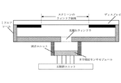
図3は本願の一実施例に係る指紋認識装置300の模式図である。
図3に示すように、指紋認識装置300はディスプレイを備えた電子機器に応用され、光学指紋センサモジュール310を備える。その指紋収集領域の少なくとも一部が該ディスプレイの表示領域内に位置するように該光学指紋センサモジュール310はディスプレイの下方に設置され、該光学指紋センサモジュール310は複数のセンサダイを備え、該複数のセンサダイの検出領域はそれぞれ該指紋収集領域中の複数のサブ領域に対応し、各センサダイは対応するサブ領域の上方からの光信号を検出する。
FIG. 3 is a schematic view of the fingerprint recognition device 300 according to an embodiment of the present application.
As shown in FIG. 3, the fingerprint recognition device 300 is applied to an electronic device including a display and includes an optical
なお、本願の実施例では、センサダイの検出領域はセンサダイの物理的に占有する領域以上である。たとえば、光学イメージング原理に基づき、各センサダイはその物理面積より大きい範囲内からの反射光を受光でき、この時、該センサダイの検出領域はその物理的に占有する領域より大きく、該検出領域は指紋収集領域中の1つのサブ領域に対応し、被験指によって該サブ領域で反射される光信号は対応する該センサダイに収集される。
好ましくは、該指紋認識装置は、ディスプレイと該光学指紋センサモジュールとの間に接続され、該光学指紋センサモジュールをディスプレイ内の該指紋収集領域の下方に固定する固定ユニットをさらに備える。
In the embodiment of the present application, the detection area of the sensor die is equal to or larger than the physically occupied area of the sensor die. For example, based on the principle of optical imaging, each sensor die can receive reflected light from a range larger than its physical area, at which time the detection area of the sensor die is larger than its physically occupied area, and the detection area is a fingerprint. Corresponding to one sub-region in the collection region, the optical signal reflected by the test finger in that sub-region is collected on the corresponding sensor die.
Preferably, the fingerprint recognition device further comprises a fixation unit that is connected between the display and the optical fingerprint sensor module and secures the optical fingerprint sensor module below the fingerprint collection area in the display.
たとえば図4に示すように、固定ユニットは光学指紋センサモジュールとディスプレイとの間に接続され、該光学指紋センサモジュールをディスプレイ内の指紋収集領域の下方に固定する。該光学指紋センサモジュールの複数のセンサダイはそれぞれ該ディスプレイ内の指紋収集領域中の複数のサブ領域に対応し、指によって各サブ領域で反射される光信号は直接対応するセンサダイに伝送される。複数のセンサダイがそれぞれ複数のサブ領域の上方からの光信号を収集すると、該指紋認識装置は該複数のサブ領域の上方からのこれら光信号に基づき指紋収集領域の上方の指に指紋認識を行うことができる。 For example, as shown in FIG. 4, the fixing unit is connected between the optical fingerprint sensor module and the display, and fixes the optical fingerprint sensor module below the fingerprint collection area in the display. Each of the plurality of sensor dies of the optical fingerprint sensor module corresponds to a plurality of sub-regions in the fingerprint collection region in the display, and the optical signal reflected by the finger in each sub-region is directly transmitted to the corresponding sensor dies. When the plurality of sensor dies each collect optical signals from above the plurality of sub-regions, the fingerprint recognition device performs fingerprint recognition on the finger above the fingerprint collection region based on these optical signals from above the plurality of sub-regions. be able to.
好ましくは、該指紋認識装置は固定ユニットをさらに備え、ディスプレイの下方にミドルフレームが接続され、該ミドルフレームの該ディスプレイ内の該指紋収集領域に対応する箇所に光漏れウィンドウが設置され、該固定ユニットは該ミドルフレームと該光学指紋センサモジュールとの間に接続され、該光学指紋センサモジュールを該ミドルフレームの該光漏れウィンドウの下方に固定する。 Preferably, the fingerprint recognition device further comprises a fixation unit, a middle frame is connected below the display, and a light leak window is installed in the middle frame corresponding to the fingerprint collection area in the display and fixed. The unit is connected between the middle frame and the optical fingerprint sensor module and secures the optical fingerprint sensor module below the light leak window of the middle frame.
たとえば図5に示すように、ディスプレイの下方に機器ミドルフレーム(ミドルフレームと略称する)が設置され、該ミドルフレームの指紋収集領域に対応する位置に光漏れウィンドウが設置される。該固定ユニットは光学指紋センサモジュールとミドルフレームとの間に接続され、該光学指紋センサモジュールをミドルフレームの光漏れウィンドウの下方に固定する。該光学指紋センサモジュールの複数のセンサダイはそれぞれ該ディスプレイ内の指紋収集領域中の複数のサブ領域に対応し、指によって各サブ領域で反射される光信号は該光漏れウィンドウを介して対応するセンサダイに伝送される。複数のセンサダイがそれぞれ複数のサブ領域の上方からの光信号を収集すると、該指紋認識装置は該複数のサブ領域の上方からのこれら光信号に基づき指紋収集領域の上方の指に指紋認識を行うことができる。 For example, as shown in FIG. 5, a device middle frame (abbreviated as a middle frame) is installed below the display, and a light leakage window is installed at a position corresponding to the fingerprint collection area of the middle frame. The fixing unit is connected between the optical fingerprint sensor module and the middle frame, and fixes the optical fingerprint sensor module below the light leakage window of the middle frame. Each of the plurality of sensor dies of the optical fingerprint sensor module corresponds to a plurality of sub-regions in the fingerprint collection region in the display, and the optical signal reflected by the finger in each sub-region corresponds to the corresponding sensor dies through the light leakage window. Is transmitted to. When the plurality of sensor dies each collect optical signals from above the plurality of sub-regions, the fingerprint recognition device performs fingerprint recognition on the finger above the fingerprint collection region based on these optical signals from above the plurality of sub-regions. be able to.
なお、本願の実施例では、該光学指紋センサモジュールに備えられるセンサダイの数も、該複数のセンサダイのサイズと分布位置も限定しない。隣接するセンサダイの接合時、所定範囲内の接合隙間が許容される。該複数のセンサダイのサイズ、分布及び数等はいずれもクライアントのニーズに応じてカスタマイズできる。 In the embodiment of the present application, the number of sensor dies provided in the optical fingerprint sensor module and the size and distribution position of the plurality of sensor dies are not limited. When joining adjacent sensor dies , a joining gap within a predetermined range is allowed. The size, distribution, number, etc. of the plurality of sensor dies can all be customized according to the needs of the client.
センサダイのサイズはそれに備えられる光検出アレイ(又は光強度検出ダイと呼称される)のサイズに応じて決定でき、該光検出アレイは複数の検出ユニット(又は感光画素と呼称される)を備える。光学指紋センサモジュールの異なるセンサダイの光検出アレイのサイズ、又は感光ユニットの数は同じであってもよく異なってもよい。
好ましくは、これら複数のセンサダイに対応する複数のサブ領域はディスプレイの両側に分布し、又は該複数のサブ領域は該ディスプレイの同一側に分布し、又は該複数のサブ領域は該ディスプレイの中間領域に分布する。
The size of the sensor die can be determined according to the size of the photodetection array (also referred to as the photointensity detection die) provided therein, the photodetection array comprising a plurality of detection units (or referred to as photosensitive pixels). The size of the photodetector array of different sensor dies of the optical fingerprint sensor module, or the number of photosensitive units may be the same or different.
Preferably, the plurality of sub-regions corresponding to these plurality of sensor dies are distributed on both sides of the display, or the plurality of sub-regions are distributed on the same side of the display, or the plurality of sub-regions are intermediate regions of the display. It is distributed in.
図6及び図7はセンサダイの分布の2種の例を示す。図6に示すように、ディスプレイの指紋収集領域は4個のサブ領域を備える。ユーザーの左手の指の指紋検出を容易にするように、2個のサブ領域はディスプレイの左側に位置し、これらの2個のサブ領域の下方に2個のセンサダイが設置され、これら2個のセンサダイのサイズは同じであってもよく異なってもよく、ユーザーの右手の指の指紋検出を容易にするように、ほかの2個のサブ領域はディスプレイの右側に位置し、これら2個のサブ領域の下方に2個のセンサダイが設置され、これら2個のセンサダイのサイズは同じであってもよく異なってもよい。ユーザーが機器にアクセスする時、左側の2個のサブ領域内に左手の指を置いて指紋認識を行ってもよく、右側の2個のサブ領域内に右手の指を置いて指紋認識を行ってもよく、指紋認識のセキュリティを向上させるように両側のサブ領域にそれぞれ左手の指と右手の指を同時に置いてもよい。 6 and 7 show two examples of sensor die distribution. As shown in FIG. 6, the fingerprint collection area of the display includes four sub-areas. Two sub-regions are located on the left side of the display and two sensor dies are placed below these two sub-regions to facilitate fingerprint detection of the user's left finger. The size of the sensor dies may be the same or different, and the other two sub-areas are located on the right side of the display to facilitate fingerprint detection of the user's right finger. Two sensor dies are installed below the area, and the sizes of these two sensor dies may be the same or different. When the user accesses the device, the finger of the left hand may be placed in the two sub-areas on the left side to perform fingerprint recognition, or the finger of the right hand may be placed in the two sub-areas on the right side to perform fingerprint recognition. Alternatively, the fingers of the left hand and the fingers of the right hand may be placed simultaneously in the sub-areas on both sides to improve the security of fingerprint recognition.
さらに、図7に示すように、ディスプレイの指紋収集領域は6個のサブ領域を備える。これら6個のサブ領域は該ディスプレイの中間位置に位置し、大面積の指紋収集領域を形成する。指は該大面積の指紋収集領域内を移動自在であり、指は該指紋収集領域内のいずれの位置に位置しても、その指紋情報が収集される。これら6個のサブ領域の下方に6個のセンサダイが対応して設置され、これらの6個のセンサダイのサイズは同じであってもよく異なってもよい。 Further, as shown in FIG. 7, the fingerprint collection area of the display includes six sub-areas. These six sub-regions are located in the middle of the display and form a large area fingerprint collection region. The finger is movable within the large area of the fingerprint collection area, and the fingerprint information is collected regardless of the position of the finger in the fingerprint collection area. Six sensor dies are correspondingly installed below these six sub-regions, and the sizes of these six sensor dies may be the same or different.
図6及び図7に示されるサブ領域の面積は同じであるが、本願ではそれに限定されず、これら複数のサブ領域の面積は異なってもよく、さらに異なる形状を有してもよい。
ディスプレイ下に1つのセンサダイのみがあり、ユーザーが指を該センサダイに対応する特定領域に置いて指紋認識を行う場合に比べて、ディスプレイ下に複数のセンサダイが分布することにより、ユーザーの指の移動範囲を拡張し、指紋認識時のユーザーエクスペリエンスを向上させることができる。且つ、複数のセンサダイが一体に接合される場合、指のより大面積の指紋情報を収集でき、指紋パスワードの長さを増加させることに相当し、指紋認識のセキュリティを向上させる。
The areas of the sub-regions shown in FIGS. 6 and 7 are the same, but the present application is not limited thereto, and the areas of the plurality of sub-regions may be different or may have different shapes.
Compared to the case where there is only one sensor die under the display and the user places the finger in a specific area corresponding to the sensor die to perform fingerprint recognition, the movement of the user's finger is caused by the distribution of the plurality of sensor dies under the display. The range can be extended to improve the user experience during fingerprint recognition. Moreover, when a plurality of sensor dies are integrally joined, fingerprint information of a larger area of the finger can be collected, which corresponds to increasing the length of the fingerprint password and improves the security of fingerprint recognition.
また、ディスプレイ下に複数のセンサダイが分布することにより、指紋収集領域の面積を拡張でき、より多くの指の指紋情報を同時に収集できる。ユーザーは複数の指を同時に置いて指紋認識を行うことができ、指紋認識のセキュリティを向上させる。たとえば、図8(a)に示すように、端末装置又は特定のアプリケーションのアクセスには2つの指の指紋を同時に認識する必要があるとすると、ユーザーが図8(a)に示される大面積の指紋収集領域内に2つの被験指を置き、それにより該指紋収集領域の下方のセンサダイによってこれら2つの指の指紋情報を収集し、より多くの指紋情報を取得する。たとえば図8(b)に示すように、端末装置又は特定のアプリケーションのアクセスには3つの指の指紋を同時に認識する必要があるとすると、ユーザーが図8(b)に示される大面積の指紋収集領域内に3つの被験指を置き、該指紋収集領域の下方のセンサダイによってこれら3つの指の指紋情報を収集し、より多くの指紋情報を取得する。 Further, by distributing a plurality of sensor dies under the display, the area of the fingerprint collection area can be expanded, and more finger fingerprint information can be collected at the same time. The user can place multiple fingers at the same time to perform fingerprint recognition, improving the security of fingerprint recognition. For example, as shown in FIG. 8 (a), if the access of the terminal device or a specific application requires the fingerprints of two fingers to be recognized at the same time, the user has a large area shown in FIG. 8 (a). Two test fingers are placed in the fingerprint collection area, whereby the fingerprint information of these two fingers is collected by the sensor die below the fingerprint collection area, and more fingerprint information is acquired. For example, as shown in FIG. 8 (b), assuming that access to a terminal device or a specific application requires simultaneous recognition of fingerprints of three fingers, the user has a large area fingerprint as shown in FIG. 8 (b). Three test fingers are placed in the collection area, and the fingerprint information of these three fingers is collected by the sensor die below the fingerprint collection area to acquire more fingerprint information.
ユーザーがより多くの有効指紋特徴を提供できることによって、FRRとFARを低減させ、指紋ロック解除の正確率を向上させ、更にユーザーエクスペリエンスを向上させる。 By allowing the user to provide more effective fingerprint features, it reduces FRR and FAR, improves the accuracy rate of fingerprint unlock, and further enhances the user experience.
なお、図6〜図8に示される場合を除き、該複数のサブ領域はディスプレイの離散的又は連続的な任意の位置に分布してもよく、さらに異なる電子機器の使用ニーズを満たすようにクライアントのニーズに応じてカスタマイズしてもよい。 Except as shown in FIGS. 6 to 8, the plurality of sub-regions may be distributed at arbitrary positions discretely or continuously on the display, and the client may further meet the usage needs of different electronic devices. It may be customized according to the needs of.
本願の実施例では、被験指が指紋収集領域の複数のサブ領域のうち一部のサブ領域の上方に位置する時、該一部のサブ領域に対応するセンサダイは動作状態にある。つまり、該指紋認識装置はユーザーの指の押圧位置に応じて、指紋画像収集を行うセンサダイを決定し、指紋画像収集を行うこれらのセンサダイが動作状態に入って光信号の収集を行い、ほかのセンサダイがスリープ状態にあり、それにより消費電力を効果的に低減させる。 In the embodiment of the present application, when the test finger is located above a part of the sub-regions of the fingerprint collection area, the sensor die corresponding to the part of the sub-regions is in the operating state. That is, the fingerprint recognition device determines sensor dies for collecting fingerprint images according to the pressing position of the user's finger, and these sensor dies for collecting fingerprint images enter an operating state to collect optical signals, and other The sensor die is in a sleep state, which effectively reduces power consumption.
たとえば、図6では、ディスプレイの左側の2つのサブ領域に指の押圧が検出されると、左側の2つのサブ領域に対応するセンサダイは動作状態に入り、該指によって反射される光信号を収集して指紋認識を行い、右側の2つのサブ領域に対応するセンサダイはスリープ状態にあり、それにより消費電力を節約する。ディスプレイの右側の2つのサブ領域に指の押圧が検出されると、右側の2つのサブ領域に対応するセンサダイは動作状態に入り、該指によって反射される光信号を収集して指紋認識を行い、左側の2つのサブ領域に対応するセンサダイはスリープ状態にあり、それにより消費電力を節約する。 For example, in FIG. 6, when a finger press is detected in the two sub-regions on the left side of the display, the sensor dies corresponding to the two sub-regions on the left side enter the operating state and collect the optical signal reflected by the finger. Fingerprint recognition is performed, and the sensor dies corresponding to the two sub-regions on the right side are in the sleep state, thereby saving power consumption. When finger pressure is detected in the two sub-regions on the right side of the display, the sensor dies corresponding to the two sub-regions on the right side enter the operating state, collect the optical signal reflected by the finger, and perform fingerprint recognition. , The sensor dies corresponding to the two sub-regions on the left are in sleep mode, thereby saving power consumption.
当然、指紋認識過程を簡略化するために、ユーザーの指が指紋収集領域の一部のサブ領域を押圧すると検出すると、該複数のセンサダイを動作状態に同時に制御してもよい。本願の実施例ではそれを限定しない。 Of course, in order to simplify the fingerprint recognition process, when it is detected that the user's finger presses a part of the sub-region of the fingerprint collection region, the plurality of sensor dies may be simultaneously controlled to the operating state. The examples of the present application do not limit it.
好ましくは、該指紋認識装置は複数の光路変調器(又は、光路調節ユニット等と呼称される)をさらに備え、該複数の光路変調器はそれぞれ該複数のセンサダイに対応し、各光路変調器は光信号を対応するセンサダイの光検出アレイ(又は、光強度検出ダイ、検出ダイ等と呼称される)にガイドする。 Preferably, the fingerprint recognition device further includes a plurality of optical path modulators (also referred to as an optical path adjusting unit or the like), the plurality of optical path modulators each correspond to the plurality of sensor dies, and each optical path modulator corresponds to the plurality of sensor dies. The optical signal is guided to the optical detection array (or light intensity detection die, detection die, etc.) of the corresponding sensor die.
又は、好ましくは、該指紋認識装置は少なくとも1つの共通光路変調器をさらに備え、各共通光路変調器は少なくとも1つのセンサダイに対応し、且つ光信号をそれぞれ対応するセンサダイの光検出アレイにガイドする。 Alternatively, preferably, the fingerprint recognition device further comprises at least one common optical path modulator, each common optical path modulator corresponds to at least one sensor die, and guides the optical signal to the light detection array of the corresponding sensor die. ..
たとえば、図7に示される6個のサブ領域に対応する6個のセンサダイの上方に1つの共通光路変調器が設置され、該共通光路変調器は光信号をそれぞれこれら6個のセンサダイの光検出アレイにガイドする。 For example, one common optical path modulator is installed above the six sensor dies corresponding to the six sub-regions shown in FIG. 7, and the common optical path modulator detects an optical signal by light detection of each of these six sensor dies. Guide to the array.
さらに、たとえば、図7に示される6個のサブ領域に対応する6個のセンサダイの上方にそれぞれ6個の光路変調器が設置され、各光路変調器は光信号をそれぞれ対応するセンサダイの光検出アレイにガイドする。 Further, for example, six optical path modulators are installed above the six sensor dies corresponding to the six sub-regions shown in FIG. 7, and each optical path modulator detects an optical signal with light from the corresponding sensor die. Guide to the array.
さらに、たとえば、図6に示される4個のサブ領域に対応する4個のセンサダイのうち、左側のサブ領域に対応するセンサダイの上方に1つの光路変調器が設置され、右側のサブ領域に対応するセンサダイの上方にもう1つの光路変調器が設置される。
該光路変調器はさらに迷光を除去して有効光信号を取得するなどに用いられる。
Further, for example, of the four sensor dies corresponding to the four sub-regions shown in FIG. 6, one optical path modulator is installed above the sensor dies corresponding to the left sub-region, and corresponds to the right sub-region. Another optical path modulator is installed above the sensor die.
The optical path modulator is further used to remove stray light to obtain an effective optical signal.
該光路変調器はたとえば、光路コリメータ、集束レンズ、マイクロレンズアレイ、光ファイバーアレイ(コア有り又はコア無し)等を備える。光学指紋センサモジュールの複数のセンサダイは異なるタイプの光路変調器と組み合わせて使用してもよく、同一タイプの光路変調器を使用してもよい。 The optical path modulator includes, for example, an optical path collimator, a focusing lens, a microlens array, an optical fiber array (with or without a core), and the like. The plurality of sensor dies of the optical fingerprint sensor module may be used in combination with different types of optical path modulators, or the same type of optical path modulators may be used.
好ましくは、該光路変調器は対応するセンサダイと一体にパッケージされ、又は、該光路変調器は該光学指紋センサモジュールとは独立した部材として該指紋認識装置の内部に取り付けられる。 Preferably, the optical path modulator is packaged integrally with the corresponding sensor die, or the optical path modulator is mounted inside the fingerprint recognition device as a member independent of the optical fingerprint sensor module.
たとえば図9に示すように、該光路変調器は、具体的には、半導体ウエハ又はシリコン酸化物又は窒化物に作製される光路コリメータであり、複数のコリメーションユニットを有し、該コリメーションユニットは該光路変調器の変調ユニットとする。具体的には、該変調ユニットは高アスペクト比を有するスルーホールであり、従って該複数のコリメーションユニットは該光路変調器のスルーホールアレイを構成する。指によって反射される反射光のうち、該スルーホールに入射した光は透過してその下方の光検出ユニットに受光され、各々の光検出ユニットは基本的にその上方のスルーホールを介してガイドされる指紋テクスチャの反射光を受光し、それにより該光検出アレイは指の指紋画像を検出できる。 For example, as shown in FIG. 9, the optical path modulator is specifically an optical path collimator made of a semiconductor wafer or silicon oxide or nitride, and has a plurality of collimation units, and the collimation unit is the collimator. It is a modulation unit of an optical path modulator. Specifically, the modulation unit is a through-hole having a high aspect ratio, and therefore the plurality of collimation units constitute a through-hole array of the optical path modulator. Of the reflected light reflected by the finger, the light incident on the through hole is transmitted and received by the photodetection unit below it, and each light detection unit is basically guided through the through hole above it. It receives the reflected light of the fingerprint texture so that the photodetection array can detect the fingerprint image of the finger.
該光路変調器がたとえば図9に示される光路コリメータを使用する場合、好ましくは、該光路変調器の各々の変調ユニットはそれぞれ光検出アレイのうちの1つの光検出ユニット(又は感光画素と呼称される)に対応し、或いは、該変調ユニットと該検出アレイの光検出ユニットは非一対一対応の関係とすることで、モアレ縞干渉を低減させ、たとえば1つの光検出ユニットは複数の変調ユニットに対応し、又は、該変調ユニットは不規則な配列方式によって該検出アレイの光検出ユニットと特定の対応関係を有しないこと実現する。該光路変調器の変調ユニットは不規則な配列方式を採用する場合、該光学指紋装置は後期ソフトウェアアルゴリズムによって各々の検出ユニットの検出した反射光を校正する。 When the optical path modulator uses, for example, the optical path collimator shown in FIG. 9, preferably, each modulation unit of the optical path modulator is referred to as one optical detection unit (or photosensitive pixel) of the optical detection array. The modulation unit and the optical detection unit of the detection array have a non-one-to-one correspondence to reduce moire fringe interference. For example, one optical detection unit can be used as a plurality of modulation units. Corresponding or realizing that the modulation unit does not have a specific correspondence with the optical detection unit of the detection array by an irregular arrangement method. When the modulation unit of the optical path modulator adopts an irregular arrangement method, the optical fingerprint device calibrates the reflected light detected by each detection unit by a late software algorithm.
さらに、たとえば図10に示すように、該光路変調器は、具体的には、半導体ウエハ又はシリコン酸化物又は窒化物に製作されるマイクロレンズアレイであり、複数のマイクロレンズを有し、該マイクロレンズは該光路変調器の変調ユニットとする。指によって反射される反射光のうち、該変調ユニットに入射した光は透過してその下方の光検出ユニットに受光され、各々の光検出ユニットは基本的にその上方のマイクロレンズを介してガイドされる指紋テクスチャの反射光を受光し、それにより該光検出アレイは指の指紋画像を検出できる。 Further, for example, as shown in FIG. 10, the optical path modulator is specifically a microlens array made of a semiconductor wafer or silicon oxide or nitride, has a plurality of microlenses, and has the micro. The lens is a modulation unit of the optical path modulator. Of the reflected light reflected by the finger, the light incident on the modulation unit is transmitted and received by the light detection unit below it, and each light detection unit is basically guided through the microlens above it. It receives the reflected light of the fingerprint texture so that the light detection array can detect the fingerprint image of the finger.
さらに、たとえば図11に示すように、該光路変調器は、具体的には、集束レンズである。該集束レンズは指紋収集領域の上方の指によって反射される光信号を光検出アレイにガイドする。各センサダイの光検出アレイの上方に1つの集束レンズが設置され、該集束レンズは光信号をその下方の対応する光検出アレイにガイドする。たとえば図12に示すように、各光検出アレイはそれぞれ対応する集束レンズを使用する。従って、複数のセンサダイは複数の光路変調器を使用する。又は、複数のセンサダイは同一光路変調器を共有し、たとえば図13に示すように、複数の光検出アレイは同一集束レンズを共有し、該集束レンズは光信号をそれぞれ複数の光検出アレイにガイドする。 Further, for example, as shown in FIG. 11, the optical path modulator is specifically a focusing lens. The focusing lens guides the light signal reflected by the finger above the fingerprint collection area into the photodetection array. A focusing lens is installed above the photodetection array of each sensor die, and the focusing lens guides the optical signal to the corresponding photodetection array below it. For example, as shown in FIG. 12, each photodetection array uses a corresponding focusing lens. Therefore, a plurality of sensor dies use a plurality of optical path modulators. Alternatively, the plurality of sensor dies share the same optical path modulator, for example, as shown in FIG. 13, a plurality of photodetecting arrays share the same focusing lens, and the focusing lens guides an optical signal to each of the plurality of photodetector arrays. To do.
好ましくは、該光路変調器が光路コリメータ又はマイクロレンズアレイである場合、該光学指紋センサモジュールは図4に示される固定方式によってディスプレイの一側に取り付けられ、該光路変調器が集束レンズである場合、該光学指紋センサモジュールは図5に示される固定方式によって装置ミドルフレームの一側に取り付けられる。
好ましくは、前記指紋認識装置は、それぞれ前記複数のセンサダイに対応する複数のフィルタリングユニットをさらに備え、各フィルタリングユニットは対応するセンサダイに伝送される光信号の波長を選択する。
Preferably, when the optical path modulator is an optical path collimator or a microlens array, the optical fingerprint sensor module is mounted on one side of the display by the fixation scheme shown in FIG. 4, and the optical path modulator is a focused lens. , The optical fingerprint sensor module is attached to one side of the device middle frame by the fixing method shown in FIG.
Preferably, the fingerprint recognition device further includes a plurality of filtering units corresponding to the plurality of sensor dies, and each filtering unit selects a wavelength of an optical signal transmitted to the corresponding sensor dies.
又は、好ましくは、前記指紋認識装置は少なくとも1つの共通フィルタリングユニットをさらに備え、各共通フィルタリングユニットは少なくとも1つのセンサダイに対応し、対応するセンサダイに伝送される光信号の波長を選択する。
指紋認識装置が1つの共通フィルタリングユニットのみを備える場合、該フィルタリングユニットは該光学指紋認識モジュールの上方に位置して、該光学指紋認識モジュールに伝送される光信号の波長を選択する。
Alternatively, preferably, the fingerprint recognition device further comprises at least one common filtering unit, each common filtering unit corresponding to at least one sensor die and selecting the wavelength of the optical signal transmitted to the corresponding sensor die.
When the fingerprint recognition device includes only one common filtering unit, the filtering unit is located above the optical fingerprint recognition module and selects the wavelength of the optical signal transmitted to the optical fingerprint recognition module.
該フィルタリングユニットによって選択される光信号の波長はたとえば、可視光波長(370 nm−780 nm)又は近赤外光波長(800 nm−1500 nm)である。該フィルタリングユニットに対応する波長以外の光信号は該フィルタリングユニットを透過して光学指紋センサの光検出アレイに到達することができない。 The wavelength of the optical signal selected by the filtering unit is, for example, the visible light wavelength (370 nm-780 nm) or the near infrared light wavelength (800 nm-1500 nm). Optical signals other than the wavelength corresponding to the filtering unit cannot pass through the filtering unit and reach the photodetection array of the optical fingerprint sensor.
好ましくは、該フィルタリングユニットは対応するセンサダイと一体にパッケージされ(たとえばコーティングの方式によってセンサダイと一体にパッケージされ)、又は、該フィルタリングユニットは対応するセンサダイの上方の光路変調器と一体にパッケージされ、又は、該フィルタリングユニットは対応するセンサダイ及び光路変調器と一体にパッケージされ、又は、該フィルタリングユニットは該光学指紋センサモジュール及び光路変調器とは独立した部材として該指紋認識装置の内部に取り付けられる。 Preferably, the filtering unit is packaged integrally with the corresponding sensor die (eg, packaged integrally with the sensor die by a coating method), or the filtering unit is packaged integrally with an optical path modulator above the corresponding sensor die. Alternatively, the filtering unit is packaged integrally with the corresponding sensor die and optical path modulator, or the filtering unit is mounted inside the fingerprint recognition device as a member independent of the optical fingerprint sensor module and the optical path modulator.
光源(たとえば、ディスプレイ等)の発する光が該ディスプレイの上方の被験指の表面に反射され、該光路変調器が指の表面から反射された反射光を変調させ、反射光をフィルタリングユニットにガイドし、該反射光がフィルタリングユニットによりフィルタリングされて光学指紋センサモジュールに受光され、前記光学指紋センサモジュールが更に受光した該反射光を検出して、指紋認識を実現する。なお、上記光学指紋装置は例示的な構造であり、具体的な実施形態では、該フィルタリングユニットの位置が前記光路変調器の下方に限定されず、たとえば、一代替実施例では、該フィルタリングユニットは前記光路変調器と前記ディスプレイとの間に設置され、すなわち前記光路変調器の上方に位置し、又は、前記指紋認識装置は、それぞれ前記光路変調器の上方と下方に設置される2層のフィルタリングユニットを備える。ほかの代替実施例では、該フィルタリングユニットは前記光路変調器の内部に集積され、さらに省略されてもよく、本願ではそれを限定しない。 Light emitted by a light source (eg, a display, etc.) is reflected onto the surface of the test finger above the display, the optical path modulator modulates the reflected light reflected from the surface of the finger, and guides the reflected light to the filtering unit. The reflected light is filtered by the filtering unit and received by the optical fingerprint sensor module, and the reflected light further received by the optical fingerprint sensor module is detected to realize fingerprint recognition. The optical fingerprint device has an exemplary structure, and in a specific embodiment, the position of the filtering unit is not limited to the lower part of the optical path modulator. For example, in one alternative embodiment, the filtering unit is The two-layer filtering installed between the optical path modulator and the display, that is, located above the optical path modulator, or the fingerprint recognition device is installed above and below the optical path modulator, respectively. Equipped with a unit. In another alternative embodiment, the filtering unit is integrated inside the optical path modulator and may be further omitted, which is not limited herein.
好ましくは、該指紋認識装置は複数の制御ユニットをさらに備え、該複数の制御ユニットはそれぞれ該複数のセンサダイに対応し、各該制御ユニットは、光信号検出を行うように、対応するセンサダイの光検出アレイを制御する。 Preferably, the fingerprint recognition device further comprises a plurality of control units, each corresponding to the plurality of sensor dies, and each control unit corresponds to the light of the corresponding sensor die so as to perform optical signal detection. Control the detection array.
該制御ユニットはさらに、該指紋認識装置を用いた装置の主制御ユニットからのコマンド及び伝送データに応答できる。 The control unit can further respond to commands and transmission data from the main control unit of the device using the fingerprint recognition device.
たとえば図14に示すように、各センサダイの光検出アレイは1つの制御ユニットによって制御され、該制御ユニットは命令によって対応する該光検出アレイを制御して対応する操作を実行させ、たとえば該光検出アレイに駆動信号を入力し且つ光検出アレイの出力する検出信号を受信し、且つ受信した検出信号に基づき指紋情報を決定する。 For example, as shown in FIG. 14, the photodetector array of each sensor die is controlled by one control unit, which controls the corresponding photodetector array by command to perform the corresponding operation, eg, the photodetector. A drive signal is input to the array, a detection signal output from the photodetection array is received, and fingerprint information is determined based on the received detection signal.
又は、好ましくは、該指紋認識装置は共通制御ユニットを備え、該共通制御ユニットは、光信号検出を行うように、該複数のセンサダイの光検出アレイを制御する。 Or, preferably, the fingerprint recognition device comprises a common control unit, the common control unit, to perform optical signal detection, for controlling the light detector array of the sensor die of said plurality of.
該共通制御ユニットはさらに、該指紋認識装置を用いた装置の主制御ユニットからのコマンド及び伝送データに応答できる。 The common control unit can further respond to commands and transmission data from the main control unit of the device using the fingerprint recognition device.
たとえば図15に示すように、該複数のセンサダイの光検出アレイはいずれも同一の制御ユニットによって制御され、該制御ユニットは命令によって複数の光検出アレイを制御して対応する操作を実行させ、たとえば一部又はすべての光検出アレイに駆動信号を入力し且つ光検出アレイの出力する検出信号を受光し、且つ受信した検出信号に基づき指紋情報を決定する。 For example, as shown in FIG. 15, the photodetector arrays of the plurality of sensor dies are all controlled by the same control unit, and the control unit controls the plurality of photodetector arrays by an instruction to perform a corresponding operation, for example. A drive signal is input to some or all of the photodetected arrays, a detection signal output from the photodetector array is received, and fingerprint information is determined based on the received detection signal.
又は、好ましくは、一部の光検出アレイは1つの制御ユニットを共有し、たとえば図6中、左側のサブ領域の下方の対応するセンサダイは1つの制御ユニットによって制御され、右側のサブ領域の下方の対応するセンサダイはもう1つの制御ユニットによって制御される。 Alternatively, preferably, some photodetector arrays share one control unit, eg, in FIG. 6, the corresponding sensor die below the left sub-region is controlled by one control unit and below the right sub-region. The corresponding sensor die of is controlled by another control unit.
又は、好ましくは、該指紋認識装置は制御ユニットを備え、該指紋認識装置を用いた装置(たとえば端末装置等)の主制御ユニットは、光信号検出を行うように該複数のセンサダイの光検出アレイを制御する。 Alternatively, preferably, the fingerprint recognition device includes a control unit, and the main control unit of the device using the fingerprint recognition device (for example, a terminal device) is an optical detection array of the plurality of sensor dies so as to perform optical signal detection. To control.
該複数のセンサダイの光検出アレイは一体にパッケージされてもよく、単独にパッケージして一体に接続されてもよく、ここでは限定しない。 The photodetector arrays of the plurality of sensor dies may be packaged integrally or packaged independently and connected integrally, without limitation.
また、該指紋認識装置は、迷光が光学指紋センサモジュールに入ることを回避する遮光装置をさらに備える。 Further, the fingerprint recognition device further includes a light blocking device to prevent the stray light from entering the optical fingerprint sensor module.
なお、本願の実施例に係る指紋認識装置は複数のセンサダイに基づき指紋認識を行い、検出した指紋情報が正当ユーザーの指紋情報であるか否かを決定する。また、好ましくは、該複数のセンサダイはさらに該指の生体特徴を検出して、該指が生体の指であるか偽装指紋であるかを判断し、又は該指のタッチ力を検出する。たとえば、該指によって反射される光信号に基づき、血糖値又は血中酸素飽和度等の情報を測定し、それにより該指が生体の指であるか偽装指紋であるかを判断する。さらに、たとえば、検出した指紋パターンの変形、指とスクリーン表面との接触面積の変化、指紋の隆起が広くなること又は血流の動的変化等に基づき、指の押圧のタッチ力を決定する。 The fingerprint recognition device according to the embodiment of the present application performs fingerprint recognition based on a plurality of sensor dies, and determines whether or not the detected fingerprint information is the fingerprint information of a legitimate user. Also, preferably, the plurality of sensor dies further detect the biological characteristics of the finger to determine whether the finger is a living body finger or a fake fingerprint, or detect the touch force of the finger. For example, based on the optical signal reflected by the finger, information such as blood glucose level or blood oxygen saturation is measured, thereby determining whether the finger is a living body finger or a fake fingerprint. Further, for example, the touch force of finger pressing is determined based on the detected deformation of the fingerprint pattern, the change in the contact area between the finger and the screen surface, the widening of the fingerprint ridge, the dynamic change in blood flow, and the like.
なお、図1〜図15中の同一パターンで充填される部分は同一機能を有することを表す。 It should be noted that the portions filled with the same pattern in FIGS. 1 to 15 have the same function.
さらに、なお、本願の実施例では、指紋認識装置300の各部材間の接続方式を限定しない。 Furthermore, in the embodiment of the present application, the connection method between the members of the fingerprint recognition device 300 is not limited.
本願の実施例は、該電子機器はディスプレイ、及び上記本願の各種の実施例に係る指紋認識装置を備える電子機器をさらに提供する。 An embodiment of the present application further provides an electronic device comprising a display and the fingerprint recognition device according to the various embodiments of the present application.
該電子機器はディスプレイを備えた任意の電子機器であり、本願の実施例に係る技術案によってアンダーディスプレイ指紋認識を実現する。 The electronic device is any electronic device provided with a display, and under-display fingerprint recognition is realized by the technical proposal according to the embodiment of the present application.
ディスプレイは上記ディスプレイ、たとえばLCDディスプレイ又はOLEDディスプレイである。 The display is the display, for example an LCD display or an OLED display.
前記ディスプレイが有機発光ダイオードディスプレイである場合、前記ディスプレイの発光層は複数の有機発光ダイオード光源を備え、前記指紋認識装置は少なくとも一部の有機発光ダイオード光源を指紋認識の励起光源とする。 When the display is an organic light emitting diode display, the light emitting layer of the display includes a plurality of organic light emitting diode light sources, and the fingerprint recognition device uses at least a part of the organic light emitting diode light sources as an excitation light source for fingerprint recognition.
なお、本願の実施例の具体例は当業者が本願の実施例をよりよく理解するためのものに過ぎず、本願の実施例の範囲を限定するものではない。 It should be noted that the specific examples of the examples of the present application are merely for those skilled in the art to better understand the examples of the present application, and do not limit the scope of the examples of the present application.
なお、本願の実施例及び添付する特許請求の範囲に使用される用語は単に特定の実施例を説明することを目的とし、本願の実施例を限定するものではない。たとえば、本願の実施例及び添付する特許請求の範囲に使用される単数形の「1種」、「上記」及び「該」は、特に断らない限り、複数形をさらに含む。 It should be noted that the terms used in the examples of the present application and the appended claims are merely for the purpose of explaining the specific examples, and are not limited to the examples of the present application. For example, the singular forms "1", "above" and "the" used in the examples of the present application and the appended claims further include the plural unless otherwise specified.
当業者であれば、本明細書に開示されている実施例を参照して説明される各例のユニットは、電子ハードウェア、コンピュータソフトウェア又はそれらの組合せによって実現できると理解でき、ハードウェアとソフトウェアの互換性を明確に説明するために、上記説明では機能に応じて各例の構成及びステップを一般的に説明する。これらの機能がハードウェアで実行されるかソフトウェアで実行されるかは、技術案の特定の用途及び設計の制約条件に応じて決められる。当業者は各特定の用応用に対応した方法を用いて上記機能を実現でき、このような実現は本願の範囲に属する。 Those skilled in the art will appreciate that the units of each example described with reference to the embodiments disclosed herein can be implemented by electronic hardware, computer software, or a combination thereof, hardware and software. In order to clearly explain the compatibility of the above, the configuration and steps of each example will be generally described according to the function. Whether these functions are performed in hardware or software depends on the specific application of the proposed technology and design constraints. Those skilled in the art can realize the above functions by using a method corresponding to each specific application, and such realization belongs to the scope of the present application.
本願の提供するいくつかの実施例では、開示するシステム、装置はほかの方式によって実現することができると理解すべきである。たとえば、上記装置の実施例は例示的であり、たとえば、前記ユニットの分割は、単にロジック機能の分割の1種であり、実際に実現する時、別の分割方式を採用してもよく、たとえば複数のユニット又は要素を別のシステムに結合又は集積してもよく、或いはいくつかの特徴を無視したり実行しなかったりする。また、表示する又は検討する結合又は直接結合又は通信接続はいくつかのインタフェース、装置又はユニットを介した間接結合又は通信接続であってもよく、電気的形態、機械的形態又はほかの形態の接続であってもよい。 It should be understood that in some of the embodiments provided by the present application, the disclosed systems and devices can be implemented by other methods. For example, the embodiment of the above device is exemplary, for example, the division of the unit is merely one type of division of the logic function, and when it is actually realized, another division method may be adopted, for example. Multiple units or elements may be combined or integrated into another system, or some features may be ignored or not implemented. Also, the coupling or direct coupling or communication connection to display or consider may be an indirect coupling or communication connection via some interface, device or unit, electrical, mechanical or other form of connection. It may be.
前記分離部材として説明されるユニットは物理的に分離したものであってもよく物理的に分離してないものであってもよく、ユニットとして表示される部材は物理ユニットであってもよく物理ユニットでなくてもよく、すなわち1つの場所に位置してもよく、複数のネットワークユニットに分散してもよい。実際の必要に応じて一部又は全部のユニットを選択して本願の実施例の技術案の目的を実現できる。 The unit described as the separation member may be physically separated or not physically separated, and the member displayed as a unit may be a physical unit or a physical unit. It does not have to be, that is, it may be located in one place, or it may be distributed to a plurality of network units. Part or all of the units can be selected as needed to achieve the objectives of the proposed technical embodiments of the present application.
また、本願の各実施例の各機能ユニットは1つの処理ユニットに集積されてもよく、単独に物理的に存在してもよく、2つ以上のユニットが1つのユニットに集積されてもよい。上記集積したユニットはハードウェアの形態で実現されてもよく、ソフトウェア機能ユニットの形態で実現されてもよい。 Further, each functional unit of each embodiment of the present application may be integrated in one processing unit, may be physically present independently, or two or more units may be integrated in one unit. The integrated unit may be realized in the form of hardware or in the form of a software function unit.
前記集積されたユニットは、ソフトウェア機能ユニットの形態で実現され独立した製品として販売又は使用される場合、コンピュータ可読記憶媒体に格納されてもよい。このような理解に基づき、本願の技術案の本質的な部分又は従来技術に貢献する部分、言い換えれば、該技術案の全部又は一部は、ソフトウェア製品の形態で具体化でき、該コンピュータソフトウェア製品は記憶媒体に格納され、コンピュータ装置(パーソナルコンピュータ、サーバ、又はネットワーク装置等)に本願の各実施例の前記方法のすべて又は一部のステップを実行させるための複数の命令を含む。上記記憶媒体はUディスク、モバイルディスク、読み出し専用メモリ(ROM、Read−Only Memory)、ランダムアクセスメモリ(RAM、Random Access Memory)、磁気ディスク又は光ディスクなどのプロクラムコードを記憶できる様々な媒体を含む。 The integrated unit may be stored in a computer-readable storage medium when realized in the form of a software functional unit and sold or used as an independent product. Based on this understanding, the essential part of the technical proposal of the present application or the part contributing to the prior art, in other words, all or part of the technical proposal can be embodied in the form of a software product, and the computer software product. Is stored in a storage medium and includes a plurality of instructions for causing a computer device (personal computer, server, network device, etc.) to perform all or part of the steps of the method of each embodiment of the present application. The storage medium includes various media capable of storing a program code such as a U disk, a mobile disk, a read-only memory (ROM, Read-Only Memory), a random access memory (RAM, Random Access Memory), a magnetic disk, or an optical disk.
以上、本願の具体的な実施形態を説明したが、本願の保護範囲を限定するものではない。当業者は本願に開示されている技術的範囲を逸脱せずに、各種の等価変更や置換を容易に想到し得、これらの変更や置換はすべて本願の保護範囲に属する。従って、本願の保護範囲は特許請求の範囲の保護範囲に準じる。 Although the specific embodiments of the present application have been described above, the scope of protection of the present application is not limited. One of ordinary skill in the art can easily conceive of various equivalent changes and substitutions without departing from the technical scope disclosed in the present application, all of which are within the scope of protection of the present application. Therefore, the scope of protection of the present application conforms to the scope of protection of the claims.
Claims (21)
前記光信号をそれぞれ対応するセンサダイの光検出アレイにガイドする少なくとも1つの光路変調器をさらに備えることを特徴とする指紋認識装置。 A fingerprint recognition device applied to an electronic device including a display, comprising an optical fingerprint sensor module installed below the display such that at least a portion of the fingerprint collection area is located within the display area of the display. The fingerprint collection region includes a plurality of sub-regions, the optical fingerprint sensor module includes a plurality of sensor dies that are integrally joined, and the detection regions of the plurality of sensor dies each correspond to the plurality of the sub-regions of the fingerprint collection region. However, each sensor die detects an optical signal from above the corresponding sub-region, and each sensor die is equipped with a plurality of optical detection units.
Fingerprint recognition device according to at least one further comprising said Rukoto the optical path modulator that guides the optical signal to an optical detector array of the corresponding sensor die.
前記光路変調器は前記光学指紋センサモジュールとは独立した部材として前記指紋認識装置の内部に取り付けられることを特徴とする請求項6〜8のいずれか一項に記載の指紋認識装置。 The optical path modulator is packaged integrally with the corresponding sensor die or
The fingerprint recognition device according to any one of claims 6 to 8, wherein the optical path modulator is mounted inside the fingerprint recognition device as a member independent of the optical fingerprint sensor module.
前記フィルタリングユニットは対応するセンサダイの上方の光路変調器と一体にパッケージされ、又は、
前記フィルタリングユニットは対応するセンサダイ及び光路変調器と一体にパッケージされ、又は、
前記フィルタリングユニットは前記光学指紋センサモジュール及び光路変調器とは独立した部材として前記指紋認識装置の内部に取り付けられることを特徴とする請求項10〜12のいずれか一項に記載の指紋認識装置。 The filtering unit is packaged integrally with the corresponding sensor die or
The filtering unit is packaged integrally with an optical path modulator above the corresponding sensor die, or
The filtering unit is packaged integrally with the corresponding sensor die and optical path modulator, or
The fingerprint recognition device according to any one of claims 10 to 12, wherein the filtering unit is mounted inside the fingerprint recognition device as a member independent of the optical fingerprint sensor module and the optical path modulator.
請求項1〜18のいずれか一項に記載の指紋認識装置と、を備えることを特徴とする電子機器。 With the display
An electronic device comprising the fingerprint recognition device according to any one of claims 1 to 18.
The display is an organic light emitting diode OLED display, the light emitting layer of the display includes a plurality of organic light emitting diode light sources, and the fingerprint recognition device uses at least a part of the organic light emitting diode light sources as an excitation light source for fingerprint recognition. The electronic device according to claim 19.
Applications Claiming Priority (1)
| Application Number | Priority Date | Filing Date | Title |
|---|---|---|---|
| PCT/CN2018/107115 WO2020056771A1 (en) | 2018-09-21 | 2018-09-21 | Fingerprint identification apparatus and electronic device |
Publications (2)
| Publication Number | Publication Date |
|---|---|
| JP2021508100A JP2021508100A (en) | 2021-02-25 |
| JP6864120B2 true JP6864120B2 (en) | 2021-04-21 |
Family
ID=65462475
Family Applications (1)
| Application Number | Title | Priority Date | Filing Date |
|---|---|---|---|
| JP2019561844A Active JP6864120B2 (en) | 2018-09-21 | 2018-09-21 | Fingerprint recognition device and electronic equipment |
Country Status (5)
| Country | Link |
|---|---|
| US (1) | US20200097699A1 (en) |
| EP (1) | EP3647995A4 (en) |
| JP (1) | JP6864120B2 (en) |
| CN (1) | CN109416737A (en) |
| WO (1) | WO2020056771A1 (en) |
Families Citing this family (41)
| Publication number | Priority date | Publication date | Assignee | Title |
|---|---|---|---|---|
| WO2019237353A1 (en) * | 2018-06-15 | 2019-12-19 | 深圳市汇顶科技股份有限公司 | In-screen biological feature recognition apparatus and electronic device |
| WO2020061748A1 (en) * | 2018-09-25 | 2020-04-02 | 深圳市汇顶科技股份有限公司 | Optical image capturing device and electronic apparatus |
| CN111310527A (en) * | 2018-12-12 | 2020-06-19 | 上海耕岩智能科技有限公司 | Under-screen image acquisition structure and electronic equipment |
| CN111725185A (en) * | 2019-03-04 | 2020-09-29 | 苏州多感科技有限公司 | Image sensor, manufacturing method thereof, image recognition method and electronic equipment |
| TWI732186B (en) * | 2019-03-08 | 2021-07-01 | 聚積科技股份有限公司 | Under-screen sensing and display device |
| CN109934157A (en) * | 2019-03-11 | 2019-06-25 | 深圳阜时科技有限公司 | A kind of backlight module, display device and electronic equipment |
| CN109902652A (en) * | 2019-03-11 | 2019-06-18 | 深圳阜时科技有限公司 | Biological characteristic detects mould group and backlight module and electronic device |
| CN110062931B (en) * | 2019-03-12 | 2021-07-16 | 深圳市汇顶科技股份有限公司 | Fingerprint identification device, fingerprint identification method and electronic equipment |
| WO2020181493A1 (en) | 2019-03-12 | 2020-09-17 | 深圳市汇顶科技股份有限公司 | Under-screen fingerprint recognition apparatus and electronic device |
| CN109815941A (en) * | 2019-03-13 | 2019-05-28 | 上海思立微电子科技有限公司 | Fingerprint identification device and electronic equipment |
| CN111695382B (en) * | 2019-03-14 | 2024-02-13 | 北京小米移动软件有限公司 | Fingerprint acquisition area determining method and fingerprint acquisition area determining device |
| CN110770749B (en) * | 2019-03-21 | 2021-09-03 | 深圳市汇顶科技股份有限公司 | Fingerprint identification device and electronic equipment |
| WO2020191600A1 (en) * | 2019-03-25 | 2020-10-01 | 深圳市汇顶科技股份有限公司 | Fingerprint recognition apparatus and electronic device |
| WO2020191596A1 (en) * | 2019-03-25 | 2020-10-01 | 深圳市汇顶科技股份有限公司 | Fingerprint recognition apparatus and electronic device |
| CN210038821U (en) | 2019-04-10 | 2020-02-07 | 深圳市汇顶科技股份有限公司 | Optical fingerprint identification device and electronic equipment |
| WO2020215187A1 (en) * | 2019-04-22 | 2020-10-29 | 深圳市汇顶科技股份有限公司 | Device for fingerprint recognition and electronic device |
| CN110071994A (en) * | 2019-04-25 | 2019-07-30 | Oppo广东移动通信有限公司 | Electronic equipment |
| CN110235142B (en) * | 2019-04-29 | 2023-09-12 | 深圳市汇顶科技股份有限公司 | Biological feature recognition device, biological feature recognition method and electronic equipment |
| CN111914593A (en) * | 2019-05-08 | 2020-11-10 | 上海耕岩智能科技有限公司 | Image acquisition method and device, storage medium and electronic equipment |
| EP3770737B1 (en) * | 2019-05-15 | 2023-02-15 | Shenzhen Goodix Technology Co., Ltd. | Fingerprint recognition method and apparatus, and electronic device |
| CN110110701A (en) * | 2019-05-21 | 2019-08-09 | 深圳市隆利科技股份有限公司 | A kind of fingerprint recognition mould group |
| CN111164609B (en) * | 2019-06-14 | 2023-10-13 | 深圳市汇顶科技股份有限公司 | Fingerprint identification device and electronic equipment |
| WO2020248286A1 (en) * | 2019-06-14 | 2020-12-17 | 深圳市汇顶科技股份有限公司 | Optical fingerprint apparatus and electronic device |
| CN110321832B (en) * | 2019-06-28 | 2021-05-18 | 维沃移动通信有限公司 | Optical module and mobile terminal |
| CN112418201A (en) * | 2019-08-22 | 2021-02-26 | 京东方科技集团股份有限公司 | Fingerprint identification module, driving method thereof and display device |
| EP3812955B1 (en) | 2019-08-28 | 2022-07-06 | Shenzhen Goodix Technology Co., Ltd. | Fingerprint detection apparatus and electronic device |
| CN112446271A (en) * | 2019-08-30 | 2021-03-05 | 指纹卡有限公司 | Biometric optical anti-spoofing |
| CN111052142B (en) * | 2019-09-06 | 2023-09-26 | 深圳市汇顶科技股份有限公司 | Fingerprint identification device and electronic equipment |
| CN110738193B (en) * | 2019-10-31 | 2024-01-12 | 维沃移动通信有限公司 | Electronic equipment |
| EP3846078A4 (en) * | 2019-11-05 | 2021-08-11 | Shenzhen Goodix Technology Co., Ltd. | Under-screen fingerprint recognition apparatus, lcd fingerprint recognition system, and electronic device |
| CN111339835A (en) * | 2020-02-06 | 2020-06-26 | 京东方科技集团股份有限公司 | Fingerprint discernment display module assembly, display device and electronic equipment under screen |
| CN111507273B (en) | 2020-04-20 | 2024-02-02 | 京东方科技集团股份有限公司 | Display panel, display device and manufacturing method of display panel |
| CN111554009B (en) * | 2020-04-23 | 2022-01-11 | 赣州深奥科技有限公司 | Fingerprint head structure |
| CN111753637A (en) * | 2020-04-30 | 2020-10-09 | 深圳市汇顶科技股份有限公司 | Fingerprint identification device and mobile electronic equipment |
| CN111708405A (en) * | 2020-06-22 | 2020-09-25 | Oppo广东移动通信有限公司 | Fingerprint identification subassembly and wearing equipment |
| CN111860296B (en) * | 2020-07-17 | 2024-04-09 | 敦泰电子(深圳)有限公司 | Optical fingerprint identification module, display module and fingerprint identification method thereof |
| EP4222637A1 (en) * | 2020-10-30 | 2023-08-09 | Google LLC | Fingerprint enrollment using collocation of a user's touch and a fingerprint sensor |
| CN112486352B (en) * | 2020-11-27 | 2022-07-12 | Tcl华星光电技术有限公司 | Touch control display panel |
| WO2022165770A1 (en) * | 2021-02-05 | 2022-08-11 | 深圳市汇顶科技股份有限公司 | Chip package structure and electronic device |
| TWI777742B (en) * | 2021-05-18 | 2022-09-11 | 友達光電股份有限公司 | Fingerprint recognition device |
| WO2023085148A1 (en) * | 2021-11-12 | 2023-05-19 | 株式会社ジャパンディスプレイ | Detection device |
Family Cites Families (13)
| Publication number | Priority date | Publication date | Assignee | Title |
|---|---|---|---|---|
| CN101672995B (en) * | 2009-09-29 | 2011-04-06 | 友达光电股份有限公司 | Sensing method |
| CN106570442B (en) * | 2015-10-09 | 2021-05-14 | 小米科技有限责任公司 | Fingerprint identification method and device |
| US10635878B2 (en) * | 2015-10-23 | 2020-04-28 | Shenzhen GOODIX Technology Co., Ltd. | Optical fingerprint sensor with force sensing capability |
| US10229316B2 (en) * | 2016-01-29 | 2019-03-12 | Synaptics Incorporated | Compound collimating system using apertures and collimators |
| CN106815573B (en) * | 2017-01-06 | 2019-11-19 | 武汉华星光电技术有限公司 | Display screen and electronic device |
| CN106991387A (en) * | 2017-03-23 | 2017-07-28 | 宇龙计算机通信科技(深圳)有限公司 | A kind of full frame fingerprint collecting method and mobile terminal |
| CN107195675B (en) * | 2017-04-27 | 2019-09-27 | Oppo广东移动通信有限公司 | Display screen, display device and mobile terminal |
| CN107194224B (en) * | 2017-04-28 | 2020-09-22 | Oppo广东移动通信有限公司 | Unlocking control method and related product |
| WO2019061535A1 (en) * | 2017-09-30 | 2019-04-04 | 深圳市汇顶科技股份有限公司 | Fingerprint recognition method, fingerprint recognition device and terminal equipment |
| CN207557977U (en) * | 2017-12-05 | 2018-06-29 | 深圳市为通博科技有限责任公司 | Optical path modulation device, fingerprint identification device and terminal device |
| CN108171037A (en) * | 2017-12-27 | 2018-06-15 | 努比亚技术有限公司 | Using startup method, terminal and computer storage media |
| CN108235750B (en) * | 2018-01-15 | 2021-06-11 | 深圳市汇顶科技股份有限公司 | Press detection method and device of fingerprint identification system and terminal equipment |
| CN108513666B (en) * | 2018-03-22 | 2022-05-17 | 深圳市汇顶科技股份有限公司 | Under-screen biological feature recognition device and electronic equipment |
-
2018
- 2018-09-21 EP EP18907464.4A patent/EP3647995A4/en not_active Ceased
- 2018-09-21 WO PCT/CN2018/107115 patent/WO2020056771A1/en unknown
- 2018-09-21 JP JP2019561844A patent/JP6864120B2/en active Active
- 2018-09-21 CN CN201880001566.2A patent/CN109416737A/en active Pending
-
2019
- 2019-08-27 US US16/551,715 patent/US20200097699A1/en not_active Abandoned
Also Published As
| Publication number | Publication date |
|---|---|
| US20200097699A1 (en) | 2020-03-26 |
| CN109416737A (en) | 2019-03-01 |
| EP3647995A1 (en) | 2020-05-06 |
| EP3647995A4 (en) | 2020-05-06 |
| JP2021508100A (en) | 2021-02-25 |
| WO2020056771A1 (en) | 2020-03-26 |
Similar Documents
| Publication | Publication Date | Title |
|---|---|---|
| JP6864120B2 (en) | Fingerprint recognition device and electronic equipment | |
| CN209962265U (en) | Fingerprint identification device and electronic equipment | |
| US11048903B2 (en) | Under-LCD screen optical sensor module for on-screen fingerprint sensing | |
| US10331939B2 (en) | Multi-layer optical designs of under-screen optical sensor module having spaced optical collimator array and optical sensor array for on-screen fingerprint sensing | |
| US10318791B2 (en) | Anti-spoofing sensing for rejecting fake fingerprint patterns in under-screen optical sensor module for on-screen fingerprint sensing | |
| US11030434B2 (en) | Lens-pinhole array designs in ultra thin under screen optical sensors for on-screen fingerprint sensing | |
| EP3465399B1 (en) | Optical collimators for under-screen optical sensor module for on-screen fingerprint sensing | |
| CN109496313B (en) | Fingerprint identification device and electronic equipment | |
| US10614283B2 (en) | Devices with peripheral task bar display zone and under-LCD screen optical sensor module for on-screen fingerprint sensing | |
| CN109791599B (en) | Under-screen optical sensor module for on-screen fingerprint sensing | |
| US10410037B2 (en) | Under-screen optical sensor module for on-screen fingerprint sensing implementing imaging lens, extra illumination or optical collimator array | |
| EP3254235B1 (en) | Under-screen optical sensor module for on-screen fingerprint sensing | |
| CN109791325B (en) | Device with peripheral taskbar display and LCD underscreen optical sensor module for on-screen fingerprint sensing | |
| CN109196525B (en) | Anti-spoof sensing to reject false fingerprint patterns in an off-screen optical sensor module for on-screen fingerprint sensing | |
| WO2020077506A1 (en) | Fingerprint recognition method and apparatus and terminal device with fingerprint recognition function | |
| US11210491B2 (en) | Fingerprint sensor under a display module with tilted receiving optics | |
| KR102374723B1 (en) | Optical Fingerprint Devices and Electronic Devices | |
| WO2020093251A1 (en) | Double sensing area-based fingerprint identification method, fingerprint identification system, and electronic device | |
| WO2020082375A1 (en) | Compound lens structure, fingerprint recognition apparatus, and electronic device | |
| WO2020168495A1 (en) | Method and device for fingerprint recognition, and terminal device | |
| CN110770750B (en) | Fingerprint identification device and electronic equipment | |
| WO2020168496A1 (en) | Method and apparatus for fingerprint recognition, and terminal device | |
| CN210534801U (en) | Fingerprint identification device and electronic equipment | |
| CN111183429B (en) | Fingerprint identification method and device and electronic equipment | |
| WO2020073166A1 (en) | Fingerprint recognition method and apparatus, and terminal device |
Legal Events
| Date | Code | Title | Description |
|---|---|---|---|
| A521 | Request for written amendment filed |
Free format text: JAPANESE INTERMEDIATE CODE: A523 Effective date: 20191108 |
|
| A621 | Written request for application examination |
Free format text: JAPANESE INTERMEDIATE CODE: A621 Effective date: 20191108 |
|
| A871 | Explanation of circumstances concerning accelerated examination |
Free format text: JAPANESE INTERMEDIATE CODE: A871 Effective date: 20191108 |
|
| A975 | Report on accelerated examination |
Free format text: JAPANESE INTERMEDIATE CODE: A971005 Effective date: 20201014 |
|
| A131 | Notification of reasons for refusal |
Free format text: JAPANESE INTERMEDIATE CODE: A131 Effective date: 20201020 |
|
| A521 | Request for written amendment filed |
Free format text: JAPANESE INTERMEDIATE CODE: A523 Effective date: 20201218 |
|
| A131 | Notification of reasons for refusal |
Free format text: JAPANESE INTERMEDIATE CODE: A131 Effective date: 20210112 |
|
| A521 | Request for written amendment filed |
Free format text: JAPANESE INTERMEDIATE CODE: A523 Effective date: 20210312 |
|
| TRDD | Decision of grant or rejection written | ||
| A01 | Written decision to grant a patent or to grant a registration (utility model) |
Free format text: JAPANESE INTERMEDIATE CODE: A01 Effective date: 20210323 |
|
| A61 | First payment of annual fees (during grant procedure) |
Free format text: JAPANESE INTERMEDIATE CODE: A61 Effective date: 20210401 |
|
| R150 | Certificate of patent or registration of utility model |
Ref document number: 6864120 Country of ref document: JP Free format text: JAPANESE INTERMEDIATE CODE: R150 |
|
| R250 | Receipt of annual fees |
Free format text: JAPANESE INTERMEDIATE CODE: R250 |