JP6832082B2 - DC / DC converter and its control circuit, inductor short circuit detection method, control method, electronic equipment - Google Patents
DC / DC converter and its control circuit, inductor short circuit detection method, control method, electronic equipment Download PDFInfo
- Publication number
- JP6832082B2 JP6832082B2 JP2016128919A JP2016128919A JP6832082B2 JP 6832082 B2 JP6832082 B2 JP 6832082B2 JP 2016128919 A JP2016128919 A JP 2016128919A JP 2016128919 A JP2016128919 A JP 2016128919A JP 6832082 B2 JP6832082 B2 JP 6832082B2
- Authority
- JP
- Japan
- Prior art keywords
- converter
- circuit
- control circuit
- short
- inductor
- Prior art date
- Legal status (The legal status is an assumption and is not a legal conclusion. Google has not performed a legal analysis and makes no representation as to the accuracy of the status listed.)
- Active
Links
- 238000001514 detection method Methods 0.000 title claims description 72
- 238000000034 method Methods 0.000 title claims description 8
- 230000001360 synchronised effect Effects 0.000 claims description 27
- 230000007423 decrease Effects 0.000 claims description 5
- 239000004065 semiconductor Substances 0.000 claims description 5
- 239000000758 substrate Substances 0.000 claims description 5
- 238000010586 diagram Methods 0.000 description 20
- 239000003990 capacitor Substances 0.000 description 6
- 102100022116 F-box only protein 2 Human genes 0.000 description 4
- 101000824158 Homo sapiens F-box only protein 2 Proteins 0.000 description 4
- 101000836005 Homo sapiens S-phase kinase-associated protein 1 Proteins 0.000 description 4
- 102100025487 S-phase kinase-associated protein 1 Human genes 0.000 description 4
- 230000005856 abnormality Effects 0.000 description 4
- 230000004048 modification Effects 0.000 description 4
- 238000012986 modification Methods 0.000 description 4
- 230000002159 abnormal effect Effects 0.000 description 3
- XAGFODPZIPBFFR-UHFFFAOYSA-N aluminium Chemical compound [Al] XAGFODPZIPBFFR-UHFFFAOYSA-N 0.000 description 2
- 229910052782 aluminium Inorganic materials 0.000 description 2
- 238000013459 approach Methods 0.000 description 2
- 238000012544 monitoring process Methods 0.000 description 2
- 230000008569 process Effects 0.000 description 2
- 230000004913 activation Effects 0.000 description 1
- 239000008186 active pharmaceutical agent Substances 0.000 description 1
- 230000008901 benefit Effects 0.000 description 1
- 230000008859 change Effects 0.000 description 1
- 230000014509 gene expression Effects 0.000 description 1
- 230000010354 integration Effects 0.000 description 1
- 238000012545 processing Methods 0.000 description 1
- 230000001105 regulatory effect Effects 0.000 description 1
- 230000004044 response Effects 0.000 description 1
Images


Landscapes
- Dc-Dc Converters (AREA)
Description
本発明は、DC/DCコンバータに関する。 The present invention relates to a DC / DC converter.
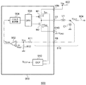
さまざまな電子機器において、ある電圧値の直流電圧を別の電圧値の直流電圧に変換するDC/DCコンバータが使用される。図1は、DC/DCコンバータ800の基本構成を示すブロック図である。図1のDC/DCコンバータ800は、降圧型(Buckコンバータ)であり、入力ライン802の入力電圧VINを降圧して目標電圧VOUT(REF)に安定化された出力電圧VOUTを生成し、出力ライン804に接続される負荷(不図示)に供給する。DC/DCコンバータ800は、出力回路810と、制御回路900を備える。出力回路810は、スイッチングトランジスタM1、同期整流トランジスタM2、インダクタL1、出力キャパシタC1を含む。制御回路900は、出力電圧VOUTが目標電圧VOUT(REF)に近づくように、スイッチングトランジスタM1および同期整流トランジスタM2のスイッチングのデューティ比をフィードバック制御する。
In various electronic devices, a DC / DC converter that converts a DC voltage of one voltage value into a DC voltage of another voltage value is used. FIG. 1 is a block diagram showing a basic configuration of the DC /
抵抗R11,R12は、フィードバック(FB)端子に入力された出力電圧VOUTを分圧し、フィードバック電圧VFBを生成する。制御回路900のエラーアンプ902は、フィードバック電圧VFBと基準電圧VREFの誤差を増幅し、誤差信号VERRを生成する。パルス変調器904は、誤差信号VERRに応じたデューティ比を有するパルス信号SPWMを生成する。ドライバ906は、パルス信号SPWMに応じてスイッチングトランジスタM1および同期整流トランジスタM2をスイッチングし、スイッチング(LX)端子に、入力電圧VINと接地電圧VGNDをとる矩形電圧VLXを発生させる。
The resistors R11 and R12 divide the output voltage V OUT input to the feedback (FB) terminal to generate a feedback voltage V FB. The
DC/DCコンバータ800は過電流保護(OCP:Over Current Protection)機能を備えるのが一般的であり、制御回路900は、OCP回路910を備える。OCP回路910は、スイッチングトランジスタM1および/または同期整流トランジスタM2に流れる電流I1,IM2を監視し、所定のしきい値を超えると、あるいはその状態が持続すると、OCP信号をアサートする。OCP信号がアサートされると、制御回路900は、スイッチングトランジスタM1および同期整流トランジスタM2のスイッチングを停止する。
The DC /
したがって図1のDC/DCコンバータ800では、過電流状態において、負荷に電力が供給できなくなる。DC/DCコンバータ800の負荷が、DC/DCコンバータ800を搭載する電子機器のメインプロセッサである場合、電子機器そのものが動作不能となってしまう。
Therefore, in the DC /
本発明は係る課題に鑑みてなされたものであり、そのある態様の例示的な目的のひとつは、異常状態においても負荷に電力を供給可能なDC/DCコンバータの提供にある。 The present invention has been made in view of the above problems, and one of the exemplary objects of the embodiment is to provide a DC / DC converter capable of supplying electric power to a load even in an abnormal state.
本発明のある態様は、複数チャンネルを有するマルチフェーズのDC/DCコンバータの制御回路に関する。制御回路は、DC/DCコンバータの出力電圧に応じたフィードバック信号とその目標値の誤差を増幅し、誤差信号を生成するエラーアンプと、誤差信号にもとづいて、複数チャンネルのパルス信号を生成するパルス変調器と、複数チャンネルに対応し、それぞれが対応するパルス信号にもとづいて、対応するスイッチングトランジスタを駆動する複数のドライバと、複数チャンネルそれぞれのインダクタのショートを検出するショート検出回路と、ショートが検出されたチャンネルの動作を停止する保護回路と、を備える。 One aspect of the present invention relates to a control circuit of a multiphase DC / DC converter having a plurality of channels. The control circuit is an error amplifier that amplifies the error between the feedback signal according to the output voltage of the DC / DC converter and its target value and generates an error signal, and a pulse that generates a pulse signal of multiple channels based on the error signal. A modulator, multiple drivers that support multiple channels and drive the corresponding switching transistors based on the corresponding pulse signals, a short-circuit detection circuit that detects short circuits in the inductors of each of the multiple channels, and short-circuit detection. It is provided with a protection circuit for stopping the operation of the channel.
この態様によると、ショートが検出されたチャンネル以外の動作を継続することにより、負荷に電力を供給し続けることができる。ショートのチャンネルについては、スイッチングを停止して、インダクタの一端をハイインピーダンスに固定することで、他のチャンネルへの影響を防止できる。 According to this aspect, power can be continuously supplied to the load by continuing the operation other than the channel in which the short circuit is detected. For short channels, stopping switching and fixing one end of the inductor to high impedance can prevent the influence on other channels.
ショート検出回路は、DC/DCコンバータのスイッチングトランジスタの電流がしきい値を超える第1過電流状態と、DC/DCコンバータの整流素子の電流がしきい値を超える第2過電流状態とが連続して発生すると、インダクタのショートと判定してもよい。
インダクタがショートすると、インダクタンスが実質的にゼロとなる。したがって、スイッチングトランジスタおよび整流素子それぞれの電流がいずれも過電流状態となる。この態様によれば、2つの過電流状態を監視することで、インダクタのショートを検出できる。
In the short-circuit detection circuit, the first overcurrent state in which the current of the switching transistor of the DC / DC converter exceeds the threshold value and the second overcurrent state in which the current of the rectifier element of the DC / DC converter exceeds the threshold value are continuous. If it occurs, it may be determined that the inductor is short-circuited.
When the inductor is short-circuited, the inductance becomes substantially zero. Therefore, the currents of the switching transistor and the rectifying element are both overcurrent. According to this aspect, the short circuit of the inductor can be detected by monitoring the two overcurrent states.
ショート検出回路は、第1過電流状態と第2過電流状態が複数サイクルにわたり連続して発生すると、インダクタのショートと判定してもよい。これにより、ノイズ等によるショートの誤検出を防止できる。 The short-circuit detection circuit may determine that the inductor is short-circuited when the first overcurrent state and the second overcurrent state occur continuously over a plurality of cycles. This makes it possible to prevent erroneous detection of a short circuit due to noise or the like.
制御回路は、スイッチングトランジスタの電流に応じた第1検出信号を所定の第1しきい値信号と比較し、第1過電流検出信号を生成する第1過電流検出コンパレータと、整流素子の電流に応じた第2検出信号を所定の第2しきい値信号と比較し、第2過電流検出信号を生成する第2過電流検出コンパレータと、をさらに備えてもよい。ショート検出回路は、第1過電流検出信号および第2過電流検出信号にもとづいて、インダクタのショートを検出してもよい。
過電流検出用のコンパレータをインダクタのショート検出に利用することで、ハードウェアの増加を抑制できる。
The control circuit compares the first detection signal corresponding to the current of the switching transistor with a predetermined first threshold signal, and uses the first overcurrent detection comparator to generate the first overcurrent detection signal and the current of the rectifying element. A second overcurrent detection comparator that compares the corresponding second detection signal with a predetermined second threshold signal and generates a second overcurrent detection signal may be further provided. The short circuit detection circuit may detect an inductor short circuit based on the first overcurrent detection signal and the second overcurrent detection signal.
By using a comparator for overcurrent detection to detect short circuits in inductors, it is possible to suppress an increase in hardware.
第1検出信号は、スイッチングトランジスタのドレインソース間電圧にもとづいて生成してもよい。整流素子は、同期整流トランジスタであり、第2検出信号は、同期整流トランジスタのドレインソース間電圧にもとづいて生成してもよい。トランジスタの既知のオン抵抗を利用することで、回路構成を簡素化できる。 The first detection signal may be generated based on the drain-source voltage of the switching transistor. The rectifying element is a synchronous rectifying transistor, and the second detection signal may be generated based on the drain-source voltage of the synchronous rectifying transistor. The circuit configuration can be simplified by utilizing the known on-resistance of the transistor.
第1検出信号は、スイッチングトランジスタに対して直列に設けられたインピーダンス素子の電圧降下、もしくは、スイッチングトランジスタと並列に接続されたレプリカトランジスタに対して直列に設けられたインピーダンス素子の電圧降下にもとづいて生成されてもよい。インピーダンス素子は抵抗であってもよいし、アルミなどの配線であってもよい。 The first detection signal is based on the voltage drop of the impedance element provided in series with the switching transistor or the voltage drop of the impedance element provided in series with the replica transistor connected in parallel with the switching transistor. It may be generated. The impedance element may be a resistor or a wiring made of aluminum or the like.
あるチャンネルにおいてインダクタのショートが検出された結果、動作チャンネルの個数が減った場合に、位相差を変更してもよい。これにより系の安定性を高めることができる。 The phase difference may be changed when the number of operating channels decreases as a result of detecting an inductor short circuit in a certain channel. This makes it possible to improve the stability of the system.
DC/DCコンバータのチャンネル数はMであり、Nチャンネル(N<M)で動作中に、あるチャンネルにおいてインダクタのショートが検出されると、不使用チャンネルのひとつを動作状態に切りかえてもよい。つまりチャンネルに空きがある場合には、それを代替利用することで、同じチャンネル数を維持できる。 The number of channels of the DC / DC converter is M, and if an inductor short circuit is detected in a certain channel during operation in N channel (N <M), one of the unused channels may be switched to the operating state. In other words, if there is a vacancy in the channel, the same number of channels can be maintained by using it as an alternative.
制御回路は、インダクタのショートが検出されたとき、外部に通知する通知部をさらに備えてもよい。 The control circuit may further include a notification unit that notifies the outside when an inductor short circuit is detected.
制御回路は、複数チャンネルそれぞれのインダクタのオープンを検出するオープン検出回路をさらに備えてもよい。保護回路は、オープンが検出されたチャンネルの動作を停止してもよい。 The control circuit may further include an open detection circuit that detects the opening of the inductor of each of the plurality of channels. The protection circuit may stop the operation of the channel where the open is detected.
あるチャンネルにおいてインダクタのオープンが検出された結果、動作チャンネルの個数が減った場合に、位相差を変更してもよい。これにより系の安定性を高めることができる。 The phase difference may be changed when the number of operating channels decreases as a result of detecting the openness of the inductor in a certain channel. This makes it possible to improve the stability of the system.
DC/DCコンバータのチャンネル数はMであり、Nチャンネル(N<M)で動作中に、あるチャンネルにおいてインダクタのオープンが検出されると、不使用チャンネルのひとつを動作状態に切りかえてもよい。これにより動作チャンネル数を維持できる。 The number of channels of the DC / DC converter is M, and one of the unused channels may be switched to the operating state when the openness of the inductor is detected in a certain channel while operating in the N channel (N <M). As a result, the number of operating channels can be maintained.
制御回路は、ひとつの半導体基板に一体集積化されてもよい。「一体集積化」とは、回路の構成要素のすべてが半導体基板上に形成される場合や、回路の主要構成要素が一体集積化される場合が含まれ、回路定数の調節用に一部の抵抗やキャパシタなどが半導体基板の外部に設けられていてもよい。 The control circuit may be integrally integrated on one semiconductor substrate. "Integrated integration" includes cases where all the components of a circuit are formed on a semiconductor substrate or cases where the main components of a circuit are integrated integrally, and some of them are used for adjusting circuit constants. A resistor, a capacitor, or the like may be provided outside the semiconductor substrate.
本発明の別の態様はDC/DCコンバータに関する。DC/DCコンバータは上述のいずれかの制御回路を備える。 Another aspect of the invention relates to a DC / DC converter. The DC / DC converter includes any of the above control circuits.
本発明の別の態様は、電子機器に関する。電子機器は、上述のDC/DCコンバータを備えてもよい。 Another aspect of the invention relates to electronic devices. The electronic device may include the above-mentioned DC / DC converter.
本発明の別の態様は、複数Mチャンネルを有するマルチフェーズのDC/DCコンバータに関する。このDC/DCコンバータは、負荷が要求する電力をNチャンネル(N<M)で供給可能であり、いずれかのチャンネルにおいて異常が検出されたとき、そのチャンネルのみを停止し、残りのチャンネルで負荷に電力を供給し続ける。 Another aspect of the invention relates to a multiphase DC / DC converter having multiple M channels. This DC / DC converter can supply the power required by the load in N channels (N <M), and when an abnormality is detected in any of the channels, only that channel is stopped and the remaining channels are loaded. Continue to supply power to.
なお、以上の構成要素の任意の組み合わせや本発明の構成要素や表現を、方法、装置、システムなどの間で相互に置換したものもまた、本発明の態様として有効である。 It should be noted that any combination of the above components or components and expressions of the present invention that are mutually replaced between methods, devices, systems, and the like are also effective as aspects of the present invention.
本発明のある態様によれば、異常状態においても負荷に電力を供給できる。 According to an aspect of the present invention, power can be supplied to the load even in an abnormal state.
以下、本発明を好適な実施の形態をもとに図面を参照しながら説明する。各図面に示される同一または同等の構成要素、部材、処理には、同一の符号を付するものとし、適宜重複した説明は省略する。また、実施の形態は、発明を限定するものではなく例示であって、実施の形態に記述されるすべての特徴やその組み合わせは、必ずしも発明の本質的なものであるとは限らない。 Hereinafter, the present invention will be described with reference to the drawings based on preferred embodiments. The same or equivalent components, members, and processes shown in the drawings shall be designated by the same reference numerals, and redundant description will be omitted as appropriate. Further, the embodiment is not limited to the invention but is an example, and all the features and combinations thereof described in the embodiment are not necessarily essential to the invention.
本明細書において、「部材Aが、部材Bと接続された状態」とは、部材Aと部材Bが物理的に直接的に接続される場合や、部材Aと部材Bが、電気的な接続状態に影響を及ぼさず、あるいは機能を阻害しない他の部材を介して間接的に接続される場合も含む。 In the present specification, "a state in which the member A is connected to the member B" means that the member A and the member B are physically directly connected, or the member A and the member B are electrically connected. It also includes cases of being indirectly connected via other members that do not affect the state or interfere with the function.
同様に、「部材Cが、部材Aと部材Bの間に設けられた状態」とは、部材Aと部材C、あるいは部材Bと部材Cが直接的に接続される場合のほか、電気的な接続状態に影響を及ぼさず、あるいは機能を阻害しない他の部材を介して間接的に接続される場合も含む。 Similarly, "a state in which the member C is provided between the member A and the member B" means that the member A and the member C, or the member B and the member C are directly connected, and also electrically. It also includes the case of being indirectly connected via another member that does not affect the connection state or interfere with the function.
また、「信号A(電圧、電流)が信号B(電圧、電流)に応じている」とは、信号Aが信号Bと相関を有することを意味し、具体的には、(i)信号Aが信号Bである場合、(ii)信号Aが信号Bに比例する場合、(iii)信号Aが信号Bをレベルシフトして得られる場合、(iv)信号Aが信号Bを増幅して得られる場合、(v)信号Aが信号Bを反転して得られる場合、(vi)あるいはそれらの任意の組み合わせ、等を意味する。「応じて」の範囲は、信号A、Bの種類、用途に応じて定まることが当業者には理解される。 Further, "the signal A (voltage, current) corresponds to the signal B (voltage, current)" means that the signal A has a correlation with the signal B, and specifically, (i) the signal A. Is signal B, (ii) signal A is proportional to signal B, (iii) signal A is obtained by level-shifting signal B, (iv) signal A is obtained by amplifying signal B. If (v) signal A is obtained by inverting signal B, it means (vi) or any combination thereof, and the like. Those skilled in the art will understand that the range of "according to" is determined according to the types and applications of signals A and B.
図2は、実施の形態に係る制御回路200を備えるDC/DCコンバータ100の回路図である。DC/DCコンバータ100は、図1と同様に、マルチチャンネル、マルチフェーズの降圧コンバータ(Buck Converter)であり、入力ライン102に直流入力電圧VINを受け、それ降圧して所定の目標電圧VOUT(REF)に安定化された出力電圧VOUTを生成し、出力ライン104に接続された負荷(不図示)に供給する。
FIG. 2 is a circuit diagram of a DC /
DC/DCコンバータ100は、Mチャンネル(Mは2以上の整数)で構成される。チャンネル数Mは任意であり、2チャンネル、3チャンネル、4チャンネル、6チャンネル、8チャンネル、12チャンネル、16チャンネルなど、DC/DCコンバータ100の用途に応じて決めればよい。
The DC /
このDC/DCコンバータ100は、負荷が要求する電力をNチャンネル(N<M)で供給可能である。たとえばM=2の場合、N=1チャンネルで、負荷の要求電力をまかなえるよう構成され、M=4の場合、N=3チャンネル(もしくは2チャンネル、もしくは1チャンネル)で、負荷の要求電力をまかなえるよう構成される。DC/DCコンバータ100は、いずれかのチャンネルにおいて異常が検出されたとき、そのチャンネルのみを停止し、残りのチャンネルで負荷に電力を供給し続ける。これがDC/DCコンバータ100の基本的な特徴である。
The DC /
以下、DC/DCコンバータ100の構成を説明する。DC/DCコンバータ100は、出力回路110および制御回路200を備える。出力回路110は、チャンネルごとに、スイッチングトランジスタM1、同期整流トランジスタM2、インダクタL1を有し、Mチャンネルに共通の出力キャパシタC1および抵抗R11,R12を有する。本実施の形態において、スイッチングトランジスタM1、同期整流トランジスタM2および抵抗R11,R12は、制御回路200に集積化されているが、外付けのディスクリート素子、チップ部品を用いてもよい。
Hereinafter, the configuration of the DC /
制御回路200は、単一の半導体基板に集積化された機能IC(Integrated Circuit)である。制御回路200には、チャンネルごとに、入力(VIN)端子、スイッチング(LX)端子、接地(GND)端子が設けられ、また全チャンネルに共通のフィードバック(FB)端子が設けられる。FB端子には、出力電圧VOUTに応じた電圧がフィードバックされる。制御回路200は、出力電圧VOUTに応じたフィードバック信号VFBがその目標値VREFに近づくように、複数チャンネルCH1〜CHMのスイッチングトランジスタM1および同期整流トランジスタM2を駆動する。
The
制御回路200は、エラーアンプ202、パルス変調器204、ドライバ206_1〜206_M、メインロジック210、ショート検出回路220、オープン検出回路230を備える。エラーアンプ202は、出力電圧VOUTに応じたフィードバック信号VFBとその目標値VREFの誤差を増幅し、誤差信号VERRを生成する。
The
パルス変調器204は、誤差信号VERRに応じたデューティ比(あるいは周波数)を有するパルス信号SPWM1〜SPWMMを生成する。パルス変調器204の構成、変調方式は特に限定されないが、たとえばピーク電流モードのパルス幅変調器を用いることができる。
複数のドライバ206は、複数チャンネルに対応する。各チャンネルのドライバ206_iは、対応するパルス信号SPWMiに応じて、対応するスイッチングトランジスタM1および同期整流トランジスタM2を駆動する。
The plurality of
メインロジック210は、制御回路200を統合的に制御するロジック回路であり、起動シーケンスの制御や、複数チャンネルの位相差などを制御する。
The
ショート検出回路220は、複数チャンネルCH1〜CHMそれぞれのインダクタL1のショートを検出する。メインロジック210の保護回路212は、ショートが検出されたチャンネルの動作を停止する。
The short
またオープン検出回路230は、複数チャンネルCH1〜CHMそれぞれのインダクタL1のオープンを検出する。保護回路212は、オープンが検出されたチャンネルの動作を停止する。
Further, the
通知部240は、インダクタのショートあるいはオープンが検出されると、外部の回路に、異常の発生を通知してもよい。通知部240は、ピン242を介してI2Cなどのバスと接続されるシリアルインタフェース回路であってもよい。あるいは通知部240は、異常の有無に応じて、ピン242の電気的状態を変化させてもよい。
When the short circuit or open of the inductor is detected, the
以上がDC/DCコンバータ100の基本構成である。続いてその動作を説明する。図3(a)、(b)は、図2のDC/DCコンバータ100の第1の保護動作を説明する図である。M=2であり、図3(a)は正常時の動作を示す。正常時には、第1チャンネルCH1のLX端子と第2チャンネルCH2のLX端子は、180度の位相差でスイッチングする。
The above is the basic configuration of the DC /
図3(b)は第1チャンネルCH1のインダクタL1がショートしたときの動作を示す。このとき、保護回路212は、第1チャンネルCH1のスイッチングトランジスタM1、同期整流トランジスタM2を両方オフとしてスイッチングを停止し、LX端子をハイインピーダンス状態とする。その結果、DC/DCコンバータ100は、第2チャンネルCH2のみがアクティブのシングルフェーズのDC/DCコンバータとして動作し続ける。
FIG. 3B shows an operation when the inductor L1 of the first channel CH1 is short-circuited. At this time, the
図4(a)、(b)は、図2のDC/DCコンバータ100の第2の保護動作を説明する図である。M=2であり、図3(a)は出力電流IOUTが小さい軽負荷状態における正常時の動作を示す。メインロジック210は、軽負荷時において、チャンネル数を減らす制御を行う。具体的には、第2チャンネルCH2を不使用チャンネルとし、スイッチングトランジスタM1、同期整流トランジスタM2をオフする。第2チャンネルCH2のLX端子はハイインピーダンスとなっており、第1チャンネルCH1のLX端子がスイッチングするシングルフェーズ動作を行う。
4 (a) and 4 (b) are diagrams for explaining the second protection operation of the DC /
図4(b)は軽負荷時において第1チャンネルCH1のインダクタL1がショートしたときの動作を示す。このとき、保護回路212は、第1チャンネルCH1のスイッチングトランジスタM1、同期整流トランジスタM2を両方オフとしてスイッチングを停止し、LX端子をハイインピーダンス状態とする。そして、不使用チャンネルであった第2チャンネルCH2を使用チャンネルに切りかえる。その結果、DC/DCコンバータ100は、第2チャンネルCH2のみがアクティブのシングルフェーズのDC/DCコンバータとして動作し続ける。
FIG. 4B shows an operation when the inductor L1 of the first channel CH1 is short-circuited under a light load. At this time, the
図5(a)、(b)は、図2のDC/DCコンバータ100の第3の保護動作を説明する図である。M=4であり、図5(a)は正常時の動作を示す。正常時には、第1チャンネルCH1のLX端子〜第4チャンネルCH4のLX端子は、90度の位相差でスイッチングしている。
5 (a) and 5 (b) are diagrams for explaining the third protection operation of the DC /
図5(b)は、第1チャンネルCH1のインダクタL1がショートしたときの動作を示す。このとき、保護回路212は、第1チャンネルCH1のスイッチングトランジスタM1、同期整流トランジスタM2を両方オフとしてスイッチングを停止し、LX端子をハイインピーダンス状態とする。その結果、DC/DCコンバータ100は、第2チャンネルCH2〜第4チャンネルCH4の3チャンネルがアクティブで動作し続ける。メインロジック210は、動作チャンネルの個数が減った場合に、変更後のアクティブなチャンネル数にもとづいて位相差を変更する。この例では、変更後のチャンネル数はN=3であるから、位相差は360度/3=120度に切りかえられる。
FIG. 5B shows an operation when the inductor L1 of the first channel CH1 is short-circuited. At this time, the
以上がDC/DCコンバータ100の動作である。
このDC/DCコンバータ100によれば、ショートが検出されたチャンネル以外の動作を継続することにより、負荷に電力を供給し続けることができる。ショートのチャンネルについては、スイッチングを停止して、インダクタの一端をハイインピーダンスに固定することで、他のチャンネルへの影響を防止できる。
The above is the operation of the DC /
According to the DC /
また図4(a)、(b)に示したように、チャンネルに空きがある場合には、空きチャンネルを代替利用することで、同じチャンネル数を維持できる。 Further, as shown in FIGS. 4A and 4B, when there is a vacancy in the channel, the same number of channels can be maintained by using the vacant channel instead.
なお、いずれかのチャンネルにおいてインダクタのオープンが検出された場合についても、同様の保護動作が実行される。 The same protection operation is executed even when the openness of the inductor is detected in any of the channels.
本発明は、図2のブロック図や回路図として把握され、あるいは上述の説明から導かれるさまざまな装置、回路に及ぶものであり、特定の構成に限定されるものではない。以下、本発明の範囲を狭めるためではなく、発明の本質や回路動作の理解を助け、またそれらを明確化するために、より具体的な構成例や実施例を説明する。 The present invention extends to various devices and circuits grasped as the block diagram and circuit diagram of FIG. 2 or derived from the above description, and is not limited to a specific configuration. Hereinafter, more specific configuration examples and examples will be described not for narrowing the scope of the present invention but for helping the understanding of the essence of the invention and the circuit operation and clarifying them.
続いて、インダクタのショート検出について説明する。
(第1ショート検出方法)
図6(a)、(b)は、第1のショート検出方法を説明する図である。図6(a)は正常時の波形図である。図6(b)は、インダクタがショートしたときの波形を示す。インダクタL1がショートすると、インダクタンスが実質的にゼロとなり、ショート経路に流れる電流IL1’のピーク値が増加する。この電流IL1’は、スイッチングトランジスタM1および同期整流トランジスタM2から供給されるため、それぞれの電流IM1,IM2がいずれも過電流状態となる。
Subsequently, short circuit detection of the inductor will be described.
(First short detection method)
6 (a) and 6 (b) are diagrams for explaining the first short-circuit detection method. FIG. 6A is a waveform diagram in a normal state. FIG. 6B shows a waveform when the inductor is short-circuited. When the inductor L1 is short-circuited, the inductance becomes substantially zero, and the peak value of the current IL1'flowing in the short-circuit path increases. Since this current IL1'is supplied from the switching transistor M1 and the synchronous rectifier transistor M2, the respective currents IM1 and IM2 are in an overcurrent state.
そこで、ショート検出回路220は、スイッチングトランジスタM1の電流IM1がしきい値IOCP1を超える第1過電流状態φ1と、整流素子である同期整流トランジスタM2の電流IM2がしきい値IOCP2を超える第2過電流状態φ2とが連続して発生すると、インダクタL1のショートと判定する。
Therefore, the short-
より好ましくは、ショート検出回路220は、第1過電流状態φ1と第2過電流状態φ2の連続が、複数サイクルにわたり連続して発生すると、インダクタのショートと判定してもよい。サイクル数は特に限定されないが、2〜5サイクル程度が好適である。これにより、ノイズ等によるショートの誤検出を防止できる。
More preferably, the short
図7は、制御回路200の過電流検出に関連する構成を示す回路図である。第1過電流検出コンパレータOCP_COMP1は、スイッチングトランジスタM1の電流IM1に応じた第1検出信号CS1を所定の第1しきい値信号IOCP1と比較し、比較結果を示す第1過電流検出(OCP)信号SOCP1を生成する。第2過電流検出コンパレータOCP_COMP2は、同期整流トランジスタM2の電流IM2に応じた第2検出信号CS2を所定の第2しきい値信号IOCP2と比較し、比較結果を示す第2過電流検出(OCP)信号SOCP2を生成する。第1OCP信号SOCP1および第2OCP信号SOCP2は、OCP回路250に供給される。OCP回路250は、通常の過電流保護のために設けられており、第1OCP信号SOCP1が数サイクルにわたり連続してアサートされた場合、あるいは第2OCP信号SOCP2が数サイクルにわたり連続してアサートされた場合に、全チャンネルのスイッチングを停止させる。
FIG. 7 is a circuit diagram showing a configuration related to overcurrent detection of the
ショート検出回路220は、第1OCP信号SOCP1および第2OCP信号SOCP2にもとづいて、インダクタL1のショートを検出する。過電流検出用のコンパレータをインダクタのショート検出に利用することで、ハードウェアの増加を抑制できる。
The short
第1検出信号CS1は、スイッチングトランジスタM1のドレインソース間電圧VDS1にもとづいて生成してもよい。同様に第2検出信号CS2は、同期整流トランジスタM2のドレインソース間電圧VDS2にもとづいて生成してもよい。トランジスタの既知のオン抵抗を利用することで、回路構成を簡素化できる。 The first detection signal CS 1 may be generated based on the drain-source voltage V DS 1 of the switching transistor M1. Similarly, the second detection signal CS 2 may be generated based on the drain-source voltage V DS 2 of the synchronous rectifier transistor M2. The circuit configuration can be simplified by utilizing the known on-resistance of the transistor.
あるいは、第1検出信号CS1および第2検出信号CS2は、スイッチングトランジスタM1および整流素子M2に直列に設けられたインピーダンス素子の電圧降下にもとづいて生成してもよい。インピーダンス素子は抵抗素子であってもよいし、アルミなどの配線であってもよい。 Alternatively, the first detection signal CS 1 and the second detection signal CS 2 may be generated based on the voltage drop of the impedance element provided in series with the switching transistor M1 and the rectifying element M2. The impedance element may be a resistance element or a wiring made of aluminum or the like.
あるいは第1検出信号CS1は、スイッチングトランジスタM1と並列にレプリカトランジスタを接続し、レプリカトランジスタに流れる電流IM1’を電圧に変換した信号であってもよい。同様に第2検出信号CS2は、同期整流トランジスタM2と並列にレプリカトランジスタを接続し、レプリカトランジスタに流れる電流IM2’を電圧に変換した信号であってもよい。 Alternatively, the first detection signal CS 1 may be a signal obtained by connecting a replica transistor in parallel with the switching transistor M1 and converting the current IM1'flowing through the replica transistor into a voltage. Similarly, the second detection signal CS 2 may be a signal obtained by connecting a replica transistor in parallel with the synchronous rectifier transistor M2 and converting the current IM2'flowing through the replica transistor into a voltage.
このように、スイッチングトランジスタM1、同期整流トランジスタM2の電流を検出する方法は特に限定されない。 As described above, the method of detecting the current of the switching transistor M1 and the synchronous rectifying transistor M2 is not particularly limited.
(第2ショート検出方法)
図6(b)に示すように、インダクタのショート状態において、スイッチングトランジスタM1、同期整流トランジスタM2それぞれの電流IM1、IM2は急峻となる。そこで電流IM1、IM2の傾きがしきい値を超える状態が連続すると、インダクタのショートと判定してもよい。
(Second short detection method)
As shown in FIG. 6 (b), in short the state of the inductor, the switching transistor M1, the synchronous rectification transistor M2 respectively current I M1, I M2 becomes steeper. Therefore, if the states in which the slopes of the currents IM1 and IM2 exceed the threshold value continue, it may be determined that the inductor is short-circuited.
(オープン検出方法)
図8は、インダクタのオープン検出回路の回路図である。図8には、1チャンネル分の構成のみが示されるが、その他のチャンネルも同様に構成することができる。オープン検出回路230は、抵抗R21,R22およびキャパシタC21を含む。抵抗R21,R22は、インダクタL1と並列に接続され、キャパシタC21は抵抗R21と並列に接続される。ノードAには、インダクタL1の電流IL1に応じた電圧が発生し、インダクタL1がオープンになるとノードAの電圧VAは低下するため、電圧VAを監視することによりオープン状態を検出できる。たとえばオープン検出回路230は、ノードAの電圧VAをしきい値VOPENと比較するコンパレータ232を含み、VA<VOPENが発生すると、インダクタL1のオープン異常と判定してもよい。コンパレータ232は制御回路200に集積化することができる。
(Open detection method)
FIG. 8 is a circuit diagram of an inductor open detection circuit. Although only the configuration for one channel is shown in FIG. 8, other channels can be configured in the same manner. The
あるいはインダクタがオープンになると、スイッチングトランジスタM1、同期整流トランジスタM2の電流が両方ゼロとなる。したがって、オープン検出回路230は、電流IM1,IM2がいずれも、ゼロ近傍に設定されたしきい値電流より小さいときに、インダクタのオープン状態と判定してもよい。
Alternatively, when the inductor is opened, the currents of both the switching transistor M1 and the synchronous rectifier transistor M2 become zero. Therefore, the
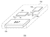
(用途)
DC/DCコンバータ100は、タブレット端末、スマートホン、ノートPC、デジタルカメラなどの電池駆動型の電子機器に搭載することができる。図9は、実施の形態に係るDC/DCコンバータ100を備える電子機器700の一例を示す図である。電子機器700は、筐体702、電池704、マイクロプロセッサ706およびDC/DCコンバータ100を備える。DC/DCコンバータ100は、その入力端子に電池704からの電池電圧VBAT(=VIN)を受け、出力端子に接続されるマイクロプロセッサ706に、出力電圧VOUTを供給する。
(Use)
The DC /
以上、本発明について、実施の形態をもとに説明した。この実施の形態は例示であり、それらの各構成要素や各処理プロセスの組み合わせにいろいろな変形例が可能なこと、またそうした変形例も本発明の範囲にあることは当業者に理解されるところである。以下、こうした変形例について説明する。 The present invention has been described above based on the embodiments. This embodiment is an example, and it will be understood by those skilled in the art that various modifications are possible for each of these components and combinations of each processing process, and that such modifications are also within the scope of the present invention. is there. Hereinafter, such a modification will be described.
DC/DCコンバータ100は、ダイオード整流型であってもよい。また降圧コンバータには限定されず、昇圧型、あるいは昇降圧型にも本発明は適用可能である。またハイサイドのトランジスタは、NチャンネルMOSFETであってもよい。またスイッチングトランジスタM1や同期整流トランジスタM2として、MOSFETに代えてIGBTやバイポーラトランジスタを用いてもよい。
The DC /
実施の形態では、あるチャンネルにおいてインダクタのオープンが検出されると、当該チャンネルのスイッチングを停止したが、スイッチングを継続してもよい。インダクタがオープンであれば、他のチャンネルには影響がないからである。ただし、実施の形態で説明したようにスイッチングを停止した場合には、無駄な電力消費を抑制でき、あるいはスイッチングノイズを低減できるという利点がある。 In the embodiment, when the openness of the inductor is detected in a certain channel, the switching of the channel is stopped, but the switching may be continued. This is because if the inductor is open, it does not affect other channels. However, when switching is stopped as described in the embodiment, there is an advantage that wasteful power consumption can be suppressed or switching noise can be reduced.
実施の形態にもとづき、具体的な語句を用いて本発明を説明したが、実施の形態は、本発明の原理、応用を示しているにすぎず、実施の形態には、請求の範囲に規定された本発明の思想を逸脱しない範囲において、多くの変形例や配置の変更が認められる。 Although the present invention has been described using specific terms and phrases based on the embodiments, the embodiments merely indicate the principles and applications of the present invention, and the embodiments are defined in the claims. Many modifications and arrangement changes are permitted without departing from the ideas of the present invention.
100…DC/DCコンバータ、102…入力ライン、104…出力ライン、110…出力回路、M1…スイッチングトランジスタ、M2…同期整流トランジスタ、L1…インダクタ、C1…出力キャパシタ、200…制御回路、202…エラーアンプ、204…パルス変調器、206…ドライバ、210…メインロジック、212…保護回路、220…ショート検出回路、230…オープン検出回路、700…電子機器、702…筐体、704…電池、706…マイクロプロセッサ。 100 ... DC / DC converter, 102 ... input line, 104 ... output line, 110 ... output circuit, M1 ... switching transistor, M2 ... synchronous rectifier transistor, L1 ... inductor, C1 ... output capacitor, 200 ... control circuit, 202 ... error Amplifier, 204 ... Pulse modulator, 206 ... Driver, 210 ... Main logic, 212 ... Protection circuit, 220 ... Short detection circuit, 230 ... Open detection circuit, 700 ... Electronic equipment, 702 ... Housing, 704 ... Battery, 706 ... Microprocessor.
Claims (17)
前記DC/DCコンバータの出力電圧に応じたフィードバック信号とその目標値の誤差を増幅し、誤差信号を生成するエラーアンプと、
前記誤差信号にもとづいて、複数チャンネルのパルス信号を生成するパルス変調器と、
複数チャンネルに対応し、それぞれが対応するパルス信号にもとづいて、対応するスイッチングトランジスタを駆動する複数のドライバと、
複数チャンネルそれぞれのインダクタのショートを検出するショート検出回路と、
ショートが検出されたチャンネルの動作を停止する保護回路と、
を備え、
前記ショート検出回路は、前記DC/DCコンバータのスイッチングトランジスタの電流がしきい値を超える第1過電流状態と、前記DC/DCコンバータの整流素子の電流がしきい値を超える第2過電流状態とが連続して発生すると、前記インダクタのショートと判定することを特徴とする制御回路。 A control circuit for a multi-phase DC / DC converter with multiple channels.
An error amplifier that amplifies the error between the feedback signal corresponding to the output voltage of the DC / DC converter and its target value and generates an error signal, and
A pulse modulator that generates a multi-channel pulse signal based on the error signal, and
Multiple drivers that support multiple channels and drive the corresponding switching transistors based on the corresponding pulse signals,
A short-circuit detection circuit that detects short circuits in the inductors of multiple channels,
A protection circuit that stops the operation of the channel where a short circuit is detected, and
With
The short-circuit detection circuit has a first overcurrent state in which the current of the switching transistor of the DC / DC converter exceeds the threshold value and a second overcurrent state in which the current of the rectifier element of the DC / DC converter exceeds the threshold value. Doo is to occur continuously, features and to that control circuit determining that short circuit the inductor.
前記DC/DCコンバータの出力電圧に応じたフィードバック信号とその目標値の誤差を増幅し、誤差信号を生成するエラーアンプと、 An error amplifier that amplifies the error between the feedback signal corresponding to the output voltage of the DC / DC converter and its target value and generates an error signal, and
前記誤差信号にもとづいて、複数チャンネルのパルス信号を生成するパルス変調器と、 A pulse modulator that generates a multi-channel pulse signal based on the error signal, and
複数チャンネルに対応し、それぞれが対応するパルス信号にもとづいて、対応するスイッチングトランジスタを駆動する複数のドライバと、 Multiple drivers that support multiple channels and drive the corresponding switching transistors based on the corresponding pulse signals,
複数チャンネルそれぞれのインダクタのショートを検出するショート検出回路と、 A short-circuit detection circuit that detects short circuits in the inductors of multiple channels,
ショートが検出されたチャンネルの動作を停止する保護回路と、 A protection circuit that stops the operation of the channel where a short circuit is detected, and
を備え、 With
前記ショート検出回路は、前記DC/DCコンバータのスイッチングトランジスタの電流がしきい値を超える第1過電流状態と、前記DC/DCコンバータの整流素子の電流がしきい値を超える第2過電流状態との連続が、複数サイクルにわたり連続して発生すると、前記インダクタのショートと判定することを特徴とする制御回路。The short-circuit detection circuit has a first overcurrent state in which the current of the switching transistor of the DC / DC converter exceeds the threshold value and a second overcurrent state in which the current of the rectifier element of the DC / DC converter exceeds the threshold value. A control circuit characterized in that when the continuation with and is continuously generated over a plurality of cycles, it is determined that the inductor is short-circuited.
前記整流素子の電流に応じた第2検出信号を所定の第2しきい値信号と比較し、第2過電流検出信号を生成する第2過電流検出コンパレータと、
をさらに備え、
前記ショート検出回路は、前記第1過電流検出信号および前記第2過電流検出信号にもとづいて、前記インダクタのショートを検出することを特徴とする請求項1または2に記載の制御回路。 A first overcurrent detection comparator that compares a first detection signal corresponding to the current of the switching transistor with a predetermined first threshold signal and generates a first overcurrent detection signal.
A second overcurrent detection comparator that compares a second detection signal corresponding to the current of the rectifying element with a predetermined second threshold signal and generates a second overcurrent detection signal.
With more
The control circuit according to claim 1 or 2 , wherein the short circuit detection circuit detects a short circuit of the inductor based on the first overcurrent detection signal and the second overcurrent detection signal.
前記第2検出信号は、前記同期整流トランジスタのドレインソース間電圧にもとづいて生成されることを特徴とする請求項3または4に記載の制御回路。 The rectifying element is a synchronous rectifying transistor and
The control circuit according to claim 3 or 4 , wherein the second detection signal is generated based on the voltage between the drain sources of the synchronous rectifier transistor.
Nチャンネル(N<M)で動作中に、あるチャンネルにおいて前記インダクタのショートが検出されると、不使用チャンネルのひとつを動作状態に切りかえることを特徴とする請求項1から7のいずれかに記載の制御回路。 The number of channels of the DC / DC converter is M.
The invention according to any one of claims 1 to 7 , wherein when a short circuit of the inductor is detected in a certain channel during operation on the N channel (N <M), one of the unused channels is switched to the operating state. Control circuit.
Nチャンネル(N<M)で動作中に、あるチャンネルにおいて前記インダクタのオープンが検出されると、不使用チャンネルのひとつを動作状態に切りかえることを特徴とする請求項10または11に記載の制御回路。 The number of channels of the DC / DC converter is M.
The control circuit according to claim 10 or 11 , wherein when the openness of the inductor is detected in a certain channel during operation in the N channel (N <M), one of the unused channels is switched to the operating state. ..
前記DC/DCコンバータのスイッチングトランジスタの電流がしきい値を超える第1過電流状態を検出するステップと、
前記DC/DCコンバータの整流素子の電流がしきい値を超える第2過電流状態を検出するステップと、
前記第1過電流状態および前記第2過電流状態が連続して発生すると、前記インダクタのショートと判定するステップと、
を備えることを特徴とする方法。 This is a method for detecting a short circuit in the inductor of a DC / DC converter.
The step of detecting the first overcurrent state in which the current of the switching transistor of the DC / DC converter exceeds the threshold value, and
A step of detecting a second overcurrent state in which the current of the rectifying element of the DC / DC converter exceeds the threshold value, and
When the first overcurrent state and the second overcurrent state occur continuously, the step of determining that the inductor is short-circuited and
A method characterized by providing.
Priority Applications (1)
| Application Number | Priority Date | Filing Date | Title |
|---|---|---|---|
| JP2016128919A JP6832082B2 (en) | 2016-06-29 | 2016-06-29 | DC / DC converter and its control circuit, inductor short circuit detection method, control method, electronic equipment |
Applications Claiming Priority (1)
| Application Number | Priority Date | Filing Date | Title |
|---|---|---|---|
| JP2016128919A JP6832082B2 (en) | 2016-06-29 | 2016-06-29 | DC / DC converter and its control circuit, inductor short circuit detection method, control method, electronic equipment |
Publications (2)
| Publication Number | Publication Date |
|---|---|
| JP2018007357A JP2018007357A (en) | 2018-01-11 |
| JP6832082B2 true JP6832082B2 (en) | 2021-02-24 |
Family
ID=60945038
Family Applications (1)
| Application Number | Title | Priority Date | Filing Date |
|---|---|---|---|
| JP2016128919A Active JP6832082B2 (en) | 2016-06-29 | 2016-06-29 | DC / DC converter and its control circuit, inductor short circuit detection method, control method, electronic equipment |
Country Status (1)
| Country | Link |
|---|---|
| JP (1) | JP6832082B2 (en) |
Families Citing this family (2)
| Publication number | Priority date | Publication date | Assignee | Title |
|---|---|---|---|---|
| US11929605B2 (en) * | 2019-11-14 | 2024-03-12 | Mitsubishi Electric Corporation | Semiconductor device |
| JP7222383B2 (en) | 2020-08-26 | 2023-02-15 | 株式会社村田製作所 | DC/DC converter parts |
Family Cites Families (5)
| Publication number | Priority date | Publication date | Assignee | Title |
|---|---|---|---|---|
| JP2006340442A (en) * | 2005-05-31 | 2006-12-14 | Mitsumi Electric Co Ltd | Multi-phase dc/dc converter and its control method |
| JP2009005555A (en) * | 2007-06-25 | 2009-01-08 | Fujitsu Ten Ltd | Step-down power supply circuit |
| JP2014128183A (en) * | 2012-12-27 | 2014-07-07 | Toyota Motor Corp | Abnormality determination apparatus and abnormality determination method for dc-dc converter |
| JP2015008603A (en) * | 2013-06-25 | 2015-01-15 | 株式会社オートネットワーク技術研究所 | Step-down device |
| JP2015073423A (en) * | 2013-09-06 | 2015-04-16 | 三星エスディアイ株式会社Samsung SDI Co.,Ltd. | Power conversion system for motor car |
-
2016
- 2016-06-29 JP JP2016128919A patent/JP6832082B2/en active Active
Also Published As
| Publication number | Publication date |
|---|---|
| JP2018007357A (en) | 2018-01-11 |
Similar Documents
| Publication | Publication Date | Title |
|---|---|---|
| US10554127B2 (en) | Control circuit and control method for multi-output DC-DC converter | |
| TWI465022B (en) | Power supply | |
| US8106640B2 (en) | Power supply control circuit, power supply device, power supply system, and method of controlling power supply control device | |
| US9998015B2 (en) | Insulated synchronous rectification DC/DC converter including a protection circuit to judge occurrence of a switching-incapable state | |
| US11349383B2 (en) | Fault protection method used in multiphase switching converters with daisy chain configuration | |
| US20160072393A1 (en) | Bidirectional current-sense circuit | |
| JP6410554B2 (en) | Switching converter and its control circuit, AC / DC converter, power adapter and electronic device | |
| JP5952809B2 (en) | Non-isolated step-down switching regulator and its control circuit, electronic equipment, AC adapter | |
| TWI694666B (en) | A converter and method of drive and control thereof | |
| JP2018129910A (en) | Dc/dc converter and control circuit thereof, control method, and on-vehicle electrical apparatus | |
| JP6794250B2 (en) | Phase compensation circuit and DC / DC converter using it | |
| EP3244518A1 (en) | Current limited power converter circuits and methods | |
| JP6875873B2 (en) | DC / DC converter and its control circuit, in-vehicle electrical equipment | |
| JP6832082B2 (en) | DC / DC converter and its control circuit, inductor short circuit detection method, control method, electronic equipment | |
| JP6704298B2 (en) | DC/DC converter and its control circuit, control method, and electronic device | |
| US9871456B2 (en) | Voltage conversion device and method of operation | |
| JP2019022303A (en) | Dc/dc converter and control circuit of the same | |
| US20230318442A1 (en) | Battery surge reduction based on early warning signal | |
| US12081125B2 (en) | Control circuit of DC/DC converter, power supply circuit, and electronic device | |
| JP6853684B2 (en) | DC / DC converter and its control circuit, control method and in-vehicle electrical equipment | |
| JP6722070B2 (en) | DC/DC converter and its control circuit, electronic device | |
| JP7028634B2 (en) | DC / DC converter control circuit, control method, power supply management circuit and electronic equipment | |
| US11949333B2 (en) | Peak current limit management for high frequency buck converter | |
| US12040711B2 (en) | Voltage regulation at load transients | |
| JP2024104224A (en) | Buck converter and its controller circuit |
Legal Events
| Date | Code | Title | Description |
|---|---|---|---|
| A621 | Written request for application examination |
Free format text: JAPANESE INTERMEDIATE CODE: A621 Effective date: 20190621 |
|
| A977 | Report on retrieval |
Free format text: JAPANESE INTERMEDIATE CODE: A971007 Effective date: 20200427 |
|
| A131 | Notification of reasons for refusal |
Free format text: JAPANESE INTERMEDIATE CODE: A131 Effective date: 20200901 |
|
| A521 | Request for written amendment filed |
Free format text: JAPANESE INTERMEDIATE CODE: A523 Effective date: 20201027 |
|
| TRDD | Decision of grant or rejection written | ||
| A01 | Written decision to grant a patent or to grant a registration (utility model) |
Free format text: JAPANESE INTERMEDIATE CODE: A01 Effective date: 20210126 |
|
| A61 | First payment of annual fees (during grant procedure) |
Free format text: JAPANESE INTERMEDIATE CODE: A61 Effective date: 20210201 |
|
| R150 | Certificate of patent or registration of utility model |
Ref document number: 6832082 Country of ref document: JP Free format text: JAPANESE INTERMEDIATE CODE: R150 |
|
| R250 | Receipt of annual fees |
Free format text: JAPANESE INTERMEDIATE CODE: R250 |