図1は、本発明の第1実施例であるDC−DCコンバータ10の異常判定装置12の構成図を示す。また、図2は、車両エンジンの自動再始動時にバッテリ電圧が低下する状況を表した図を示す。
FIG. 1 shows a configuration diagram of an abnormality determination device 12 of a DC-DC converter 10 according to a first embodiment of the present invention. Moreover, FIG. 2 shows the figure showing the condition where a battery voltage falls at the time of the automatic restart of a vehicle engine.
本実施例のDC−DCコンバータ10は、例えば、車両に搭載されており、車載バッテリの出力電圧を昇圧して車載電気負荷に電力供給を行う装置であって、具体的には、アイドリングストップシステム搭載車両におけるエンジンの自動再始動時にバックアップ電源確保等のために昇圧動作を行う昇圧装置である。DC−DCコンバータ10は、バッテリ14と電気負荷16との間に介在されている。
The DC-DC converter 10 of the present embodiment is mounted on a vehicle, for example, and is a device that boosts the output voltage of an in-vehicle battery and supplies power to the in-vehicle electric load. Specifically, the idling stop system This is a boosting device that performs a boosting operation for securing a backup power source or the like when an engine is automatically restarted in an onboard vehicle. The DC-DC converter 10 is interposed between the battery 14 and the electric load 16.
バッテリ14は、蓄えている電力を所定電圧(通常は、例えば12ボルト)で外部出力することが可能な車載バッテリである。また、電気負荷16は、バッテリ14の電圧又はそのバッテリ電圧よりも高い電圧で作動する電気負荷であって、エンジン停止時のタイミングにもまたエンジン再始動時のタイミングにも作動し得る電気負荷である。電気負荷16は、例えば、車両に搭載されるエンジンスタータやブレーキユニット,ランプユニット,メータユニット,電子制御ユニット(ECU),オーディオなどであればよく、複数設けられていてもよい。
The battery 14 is an in-vehicle battery capable of outputting stored electric power at a predetermined voltage (usually, for example, 12 volts). The electric load 16 is an electric load that operates at the voltage of the battery 14 or a voltage higher than the battery voltage, and can operate at the timing when the engine is stopped or at the timing when the engine is restarted. is there. The electric load 16 may be, for example, an engine starter, a brake unit, a lamp unit, a meter unit, an electronic control unit (ECU), an audio, or the like mounted on the vehicle, and a plurality of electric loads 16 may be provided.
DC−DCコンバータ10は、インダクタ20と、スイッチング素子22と、ダイオード24と、コンデンサ26と、からなる昇圧回路28を備えている。インダクタ20は、所定のインダクタンス値Lを有するチョークコイルである。インダクタ20の一端は、DC−DCコンバータ10すなわち昇圧回路28の入力端子として、バッテリ14に接続されている。インダクタ20の一端には、バッテリ14の電圧が入力電圧Viとして入力される。インダクタ20の他端には、スイッチング素子22が接続されている。スイッチング素子22は、インダクタ20の他端と接地端との間に介在されている。スイッチング素子22は、後述の昇圧制御ICからの指令に従ってオン/オフされる例えばMOS−FETなどである。
The DC-DC converter 10 includes a booster circuit 28 including an inductor 20, a switching element 22, a diode 24, and a capacitor 26. The inductor 20 is a choke coil having a predetermined inductance value L. One end of the inductor 20 is connected to the battery 14 as an input terminal of the DC-DC converter 10, that is, the booster circuit 28. The voltage of the battery 14 is input to one end of the inductor 20 as the input voltage Vi. A switching element 22 is connected to the other end of the inductor 20. The switching element 22 is interposed between the other end of the inductor 20 and the ground end. The switching element 22 is, for example, a MOS-FET that is turned on / off in accordance with a command from a step-up control IC described later.
インダクタ20の他端には、また、ダイオード24のアノード端子が接続されている。ダイオード24のカソード端子には、電力を蓄えることが可能なコンデンサ26の一端が接続されている。コンデンサ26は、ダイオード24のカソード端子と接地端との間に介在されている。また、ダイオード24のカソード端子及びコンデンサ26の一端は、DC−DCコンバータ10すなわち昇圧回路28の出力端子として、上記の電気負荷16に接続されている。DC−DCコンバータ10すなわち昇圧回路28は、スイッチング素子22のオン/オフによりバッテリ14の出力電圧を昇圧して電気負荷16へ電力供給を行う。
The anode terminal of the diode 24 is connected to the other end of the inductor 20. One end of a capacitor 26 capable of storing electric power is connected to the cathode terminal of the diode 24. The capacitor 26 is interposed between the cathode terminal of the diode 24 and the ground terminal. The cathode terminal of the diode 24 and one end of the capacitor 26 are connected to the electric load 16 as an output terminal of the DC-DC converter 10, that is, the booster circuit 28. The DC-DC converter 10, that is, the booster circuit 28 boosts the output voltage of the battery 14 by turning on / off the switching element 22 and supplies power to the electric load 16.
かかる昇圧回路28においては、スイッチング素子22がオフされた状態でバッテリ14からインダクタ20の一端に入力電圧Viが印加されると、インダクタ20に電流が流れてそのインダクタ20が充電される。そして、スイッチング素子22がオフからオンへ切り替わると、以後、インダクタ20に流れる電流が時間の経過に伴って比例的に増加することで、インダクタ20に蓄えられる電力が時間の経過に伴って増加すると共に、コンデンサ26から電気負荷16へ向けて電力が供給される。
In the booster circuit 28, when the input voltage Vi is applied from the battery 14 to one end of the inductor 20 with the switching element 22 turned off, a current flows through the inductor 20 and the inductor 20 is charged. When the switching element 22 is switched from off to on, the current flowing through the inductor 20 increases proportionally with the passage of time, so that the power stored in the inductor 20 increases with the passage of time. At the same time, electric power is supplied from the capacitor 26 toward the electric load 16.
次に、スイッチング素子22がオンからオフへ切り替わると、以後、インダクタ20に流れる電流がダイオード24を経由して電気負荷16側へ流れると共に、インダクタ20に蓄えられていた電力が電気負荷16へ向けて放出されて、その電流が時間の経過に伴って比例的に減少する。この際には、昇圧回路28の出力電圧Voが、入力電圧(すなわち、バッテリ14の電圧)Viとインダクタ20で発生する電圧との合計値となるので、その入力電圧Viよりも高くなると共に、また、コンデンサ26が、その入力電圧Viよりも高い出力電圧Voで充電される。
Next, when the switching element 22 is switched from on to off, the current flowing through the inductor 20 flows to the electric load 16 side via the diode 24 and the electric power stored in the inductor 20 is directed to the electric load 16. And the current decreases proportionally over time. At this time, the output voltage Vo of the booster circuit 28 becomes the total value of the input voltage (that is, the voltage of the battery 14) Vi and the voltage generated in the inductor 20, and thus becomes higher than the input voltage Vi. Further, the capacitor 26 is charged with an output voltage Vo higher than the input voltage Vi.
そして、スイッチング素子22がオフからオンへ切り替わると、以後、再び、時間の経過に伴ってインダクタ20に流れる電流が比例的に増加しインダクタ20に蓄えられる電力が増加してインダクタ20の充電が行われると共に、コンデンサ26から電気負荷16へ向けて入力電圧Viよりも高い電圧で電力が供給される。その後は、スイッチング素子22のオン/オフが所定周期で繰り返し行われる。かかる動作によれば、昇圧回路28が常に入力電圧Viよりも高い電圧Voを出力するDC−DCコンバータ10による昇圧が実現される。
Then, when the switching element 22 is switched from off to on, the current flowing through the inductor 20 increases proportionally again with the passage of time, and the power stored in the inductor 20 increases to charge the inductor 20. In addition, power is supplied from the capacitor 26 to the electric load 16 at a voltage higher than the input voltage Vi. Thereafter, the switching element 22 is turned on / off repeatedly at a predetermined cycle. According to such an operation, boosting by the DC-DC converter 10 in which the booster circuit 28 always outputs a voltage Vo higher than the input voltage Vi is realized.
DC−DCコンバータ10は、また、上記の如き昇圧回路28での昇圧動作を制御する昇圧制御IC30を備えている。昇圧制御IC30は、昇圧制御回路32、及び、その昇圧制御回路32に接続されるゲートドライバ34を有している。昇圧制御回路32は、通常時においてスイッチング素子22のオン/オフを制御する回路である。昇圧制御回路32は、自車両エンジンの自動停止条件の成立に伴うアイドリングストップ後、エンジンの自動再始動条件が成立するか否かの情報に基づいて、スイッチング素子22のオン/オフを制御する。
The DC-DC converter 10 also includes a boost control IC 30 that controls the boost operation in the boost circuit 28 as described above. The boost control IC 30 includes a boost control circuit 32 and a gate driver 34 connected to the boost control circuit 32. The step-up control circuit 32 is a circuit that controls on / off of the switching element 22 in a normal state. The boost control circuit 32 controls on / off of the switching element 22 based on information on whether or not the automatic engine restart condition is satisfied after the idling stop associated with the automatic vehicle engine stop condition being satisfied.
具体的には、昇圧制御回路32は、上記の自動再始動条件が成立しないと判別した場合は、昇圧回路28での昇圧が行われないように、スイッチング素子22をオフする指令をゲートドライバ34に対して供給し、一方、上記の自動再始動条件が成立すると判別した場合は、昇圧回路28での昇圧が適切に行われるように、上記の如くスイッチング素子22をオン/オフする指令をゲートドライバ34に対して供給する。ゲートドライバ34は、スイッチング素子22のゲートに接続されている。ゲートドライバ34は、昇圧制御回路32からの指令に従ってスイッチング素子22をオン/オフ駆動する。
Specifically, when the boost control circuit 32 determines that the automatic restart condition is not satisfied, the gate driver 34 issues a command to turn off the switching element 22 so that the boost circuit 28 does not perform boost. On the other hand, if it is determined that the above automatic restart condition is satisfied, the command to turn on / off the switching element 22 as described above is gated so that the boosting in the booster circuit 28 is appropriately performed. Supply to the driver 34. The gate driver 34 is connected to the gate of the switching element 22. The gate driver 34 drives the switching element 22 on / off according to a command from the boost control circuit 32.
尚、上記したエンジンの自動停止条件は、例えば、車両運転者によるブレーキペダルの踏み込み操作が行われていることや車速がエンジン停止速度以下であることなどである。また、上記したエンジンの自動再始動条件は、例えば、エンジン停止状態においてブレーキペダルの踏み込み操作が解除されたことやアクセルペダルの踏み込み操作が行われたことなどである。
The engine automatic stop conditions described above are, for example, that the driver depresses the brake pedal and the vehicle speed is equal to or lower than the engine stop speed. Further, the above-described automatic engine restart conditions are, for example, that the brake pedal depression operation has been released or the accelerator pedal depression operation has been performed while the engine is stopped.
従って、本実施例においては、図2に示す如く、アイドリングストップ後のエンジンの自動再始動時、バッテリ14の電圧が低下するときにも、昇圧制御回路32によりスイッチング素子22のオン/オフ駆動を行うことで、そのバッテリ電圧が通常の電圧(例えば、バッテリ14の目標電圧)まで昇圧された昇圧電源を生成することができる。このため、本実施例によれば、エンジンの自動再始動時にもDC−DCコンバータ10から電気負荷16へ安定した電圧を印加することができ、エンジンの自動再始動前後のタイミングにおいて電気負荷16を適切に継続して作動させることができる。
Therefore, in this embodiment, as shown in FIG. 2, when the engine is automatically restarted after idling is stopped, the switching element 22 is turned on / off by the boost control circuit 32 even when the voltage of the battery 14 decreases. By doing so, it is possible to generate a boosted power source whose battery voltage is boosted to a normal voltage (for example, the target voltage of the battery 14). For this reason, according to the present embodiment, a stable voltage can be applied from the DC-DC converter 10 to the electric load 16 even when the engine is automatically restarted. It can be operated properly and continuously.
本実施例のDC−DCコンバータ10において、スイッチング素子22(具体的には、ソース端子)の下流側には、抵抗36が設けられている。すなわち、抵抗36は、スイッチング素子22と接地端との間に介在されている。抵抗36は、スイッチング素子22から接地端へ向けて流れる電流の大きさを検出するための電流検出抵抗である。抵抗36の両端は、昇圧制御IC30に内蔵された電流検出アンプ38の入力端子に接続されている。電流検出アンプ38は、スイッチング素子22から接地端へ向けて流れる電流の大きさIに応じた信号を出力するアンプである。
In the DC-DC converter 10 of this embodiment, a resistor 36 is provided on the downstream side of the switching element 22 (specifically, the source terminal). That is, the resistor 36 is interposed between the switching element 22 and the ground terminal. The resistor 36 is a current detection resistor for detecting the magnitude of the current flowing from the switching element 22 toward the ground terminal. Both ends of the resistor 36 are connected to input terminals of a current detection amplifier 38 built in the boost control IC 30. The current detection amplifier 38 is an amplifier that outputs a signal corresponding to the magnitude I of the current flowing from the switching element 22 toward the ground terminal.
昇圧制御IC30は、また、制御部40、スイッチ42、及び検査用回路44を有している。上記した電流検出アンプ38の出力端子は、スイッチ42を介して昇圧制御回路32及び検査用回路44に接続されている。スイッチ42は、電流検出アンプ38の出力端子を昇圧制御回路32及び検査用回路44の何れか一方に選択的に接続させるための切替器である。スイッチ42は、通常は、電流検出アンプ38の出力端子を昇圧制御回路32に接続させる。
The step-up control IC 30 also includes a control unit 40, a switch 42, and an inspection circuit 44. The output terminal of the current detection amplifier 38 is connected to the boost control circuit 32 and the inspection circuit 44 via the switch 42. The switch 42 is a switch for selectively connecting the output terminal of the current detection amplifier 38 to one of the boost control circuit 32 and the inspection circuit 44. The switch 42 normally connects the output terminal of the current detection amplifier 38 to the boost control circuit 32.
電流検出アンプ38の出力端子がスイッチ42により昇圧制御回路32に接続されている場合、その電流検出アンプ38の出力信号は、昇圧制御回路32に供給される。昇圧制御回路32は、昇圧回路28での昇圧動作中にスイッチング素子22に流れる過電流を検出する過電流検出機能を有している。昇圧制御回路32は、電流検出アンプ38の出力信号に基づいてスイッチング素子22に流れる電流Iを検出し、その検出電流Iがスイッチング素子22などを破壊し得る異常値に達しているか否かを判別する。
When the output terminal of the current detection amplifier 38 is connected to the boost control circuit 32 by the switch 42, the output signal of the current detection amplifier 38 is supplied to the boost control circuit 32. The step-up control circuit 32 has an overcurrent detection function for detecting an overcurrent flowing through the switching element 22 during the step-up operation in the step-up circuit 28. The boost control circuit 32 detects the current I flowing through the switching element 22 based on the output signal of the current detection amplifier 38, and determines whether or not the detected current I has reached an abnormal value that can destroy the switching element 22 and the like. To do.
その結果、昇圧制御回路32は、スイッチング素子22の電流Iが異常値に達していないと判別した場合は、昇圧回路28での昇圧動作を実行し、通常どおり、スイッチング素子22のオン/オフを制御する。一方、スイッチング素子22の電流Iが異常値に達していると判別した場合は、昇圧回路28での昇圧動作を中止し、スイッチング素子22をオフさせる。
As a result, when the boost control circuit 32 determines that the current I of the switching element 22 has not reached the abnormal value, the boost control circuit 32 performs a boost operation in the boost circuit 28 and turns on / off the switching element 22 as usual. Control. On the other hand, when it is determined that the current I of the switching element 22 has reached an abnormal value, the boosting operation in the boosting circuit 28 is stopped and the switching element 22 is turned off.
従って、本実施例においては、昇圧回路28での昇圧動作中にスイッチング素子22に過電流が流れる異常が発生するか否かに応じて、その昇圧動作を中止することができる。このため、本実施例によれば、過電流発生時にスイッチング素子22を過電流や発熱から保護することができる。
Therefore, in this embodiment, the boosting operation can be stopped depending on whether or not an abnormality occurs in which the overcurrent flows in the switching element 22 during the boosting operation in the boosting circuit 28. For this reason, according to the present embodiment, the switching element 22 can be protected from overcurrent and heat generation when an overcurrent occurs.
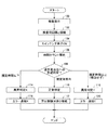
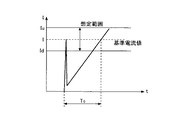
図3は、本実施例の異常判定装置12においてDC−DCコンバータ10に異常が発生していることが判定された際の具体的な故障箇所を列挙した表の一例を示す。図4は、本実施例の異常判定装置12においてDC−DCコンバータ10の異常を判定する手法を説明するための図を示す。また、図5は、本実施例の異常判定装置12において昇圧制御IC30がDC−DCコンバータ10の異常を判定すべく実行する制御ルーチンの一例のフローチャートを示す。
FIG. 3 shows an example of a table listing specific failure locations when it is determined that an abnormality has occurred in the DC-DC converter 10 in the abnormality determination device 12 of the present embodiment. FIG. 4 is a diagram for explaining a method for determining an abnormality of the DC-DC converter 10 in the abnormality determination device 12 of the present embodiment. FIG. 5 shows a flowchart of an example of a control routine executed by the boost control IC 30 in the abnormality determination device 12 of this embodiment so as to determine abnormality of the DC-DC converter 10.
本実施例の異常判定装置12は、昇圧制御IC30に内蔵される検査用回路44を備えている。検査用回路44は、インダクタ20のショートやスイッチング素子22の異常などのDC−DCコンバータ10の異常を判定するための回路である。検査用回路44には、制御部40によるスイッチ42の切り替えによって電流検出アンプ38の出力端子が接続され得る。
The abnormality determination device 12 of the present embodiment includes an inspection circuit 44 built in the boost control IC 30. The inspection circuit 44 is a circuit for determining an abnormality of the DC-DC converter 10 such as a short circuit of the inductor 20 or an abnormality of the switching element 22. The output terminal of the current detection amplifier 38 can be connected to the inspection circuit 44 by switching the switch 42 by the control unit 40.
制御部40には、DC−DCコンバータ10の異常判定を行うべき検査指示が入力される。制御部40は、かかる検査指示に従って、電流検出アンプ38の出力端子を検査用回路44に接続させるようにスイッチ42の切り替えを行う。スイッチ42は、制御部40からの検査指示に基づく切替指示に従って、電流検出アンプ38の出力端子を検査用回路44に接続させ、上記した接続の切替を行う。
The control unit 40 receives an inspection instruction to be used to determine abnormality of the DC-DC converter 10. In accordance with the inspection instruction, the control unit 40 switches the switch 42 so that the output terminal of the current detection amplifier 38 is connected to the inspection circuit 44. The switch 42 connects the output terminal of the current detection amplifier 38 to the inspection circuit 44 in accordance with the switching instruction based on the inspection instruction from the control unit 40, and performs the above-described connection switching.
尚、制御部40に上記の検査指示が入力されるタイミングは、昇圧回路28での昇圧動作中では無く、その非動作時であって、昇圧回路28の入力電圧(すなわち、バッテリ電圧)Viが安定するタイミング(例えば、アイドリングストップ直前のタイミングなど)である。また、制御部40は、検査指示に基づくスイッチ42への切替指示を後述のDC−DCコンバータ10の異常を判定するのに必要十分な時間継続して行うものとすればよく、スイッチ42が電流検出アンプ38の出力端子を検査用回路44に接続させる状態は、DC−DCコンバータ10の異常を判定するのに必要十分な時間だけ継続されるものとすればよい。
Note that the timing at which the above-described inspection instruction is input to the control unit 40 is not during the boosting operation in the booster circuit 28 but is in the non-operational state, and the input voltage (ie, battery voltage) Vi of the booster circuit 28 is It is a stable timing (for example, a timing immediately before idling stop). Moreover, the control part 40 should just perform the switching instruction | indication to the switch 42 based on a test | inspection instruction continuously for the time sufficient for determining the abnormality of the below-mentioned DC-DC converter 10, and the switch 42 is electric current. The state in which the output terminal of the detection amplifier 38 is connected to the inspection circuit 44 may be continued for a time sufficient for determining the abnormality of the DC-DC converter 10.
電流検出アンプ38の出力端子がスイッチ42により検査用回路44に接続されている場合、その電流検出アンプ38の出力信号は、検査用回路44に供給される。検査用回路44には、上記した制御部40が接続されていると共に、上記したゲートドライバ34が接続されている。制御部40は、入力された検査指示に従って、検査用回路44に対してDC−DCコンバータ10の異常判定を行うことを指令する実行指示を発する。検査用回路44は、制御部40からの実行指示に従って、電流検出アンプ38の出力信号に基づいてスイッチング素子22に流れる電流Iを検出し、その検出電流Iに基づいてDC−DCコンバータ10の異常を判定する。
When the output terminal of the current detection amplifier 38 is connected to the inspection circuit 44 by the switch 42, the output signal of the current detection amplifier 38 is supplied to the inspection circuit 44. The inspection circuit 44 is connected to the control unit 40 and the gate driver 34 described above. The control unit 40 issues an execution instruction to instruct the inspection circuit 44 to perform abnormality determination of the DC-DC converter 10 in accordance with the input inspection instruction. The inspection circuit 44 detects the current I flowing through the switching element 22 based on the output signal of the current detection amplifier 38 in accordance with the execution instruction from the control unit 40, and the abnormality of the DC-DC converter 10 based on the detected current I. Determine.
以下、本実施例において、DC−DCコンバータ10の異常を判定する具体的な手法について説明する。
Hereinafter, a specific method for determining an abnormality of the DC-DC converter 10 in this embodiment will be described.
上述の如く、スイッチング素子22がオンされると、以後、インダクタ20に流れる電流が増加する。この際、インダクタ20に流れる電流は、昇圧回路28の入力電圧Viとそのインダクタンス値Lとに応じた傾き(Vi/L)で変化する。このため、スイッチング素子22がオフからオンに切り替わると、以後、インダクタ20からスイッチング素子22を経由して接地側へ流れる電流I(t)は、次式(1)に示す如く、昇圧回路28の入力電圧Viとインダクタンス値Lとスイッチング素子22のオン継続時間tとに応じた値となる。
As described above, when the switching element 22 is turned on, the current flowing through the inductor 20 thereafter increases. At this time, the current flowing through the inductor 20 changes with a slope (Vi / L) corresponding to the input voltage Vi of the booster circuit 28 and the inductance value L thereof. For this reason, when the switching element 22 is switched from OFF to ON, the current I (t) flowing from the inductor 20 to the ground side via the switching element 22 is changed as shown in the following equation (1). The values correspond to the input voltage Vi, the inductance value L, and the ON duration t of the switching element 22.
I(t)=Vi/L×t ・・・(1)
スイッチング素子22のオン中、インダクタンス値Lは通常は一定値であるので、昇圧回路28の入力電圧Viが安定しかつDC−DCコンバータ10が正常状態にあれば、スイッチング素子22に流れる電流Iは、スイッチング素子22のオン継続時間tに時間比例して一定割合で増加する。一方、昇圧回路28の入力電圧Viが変動し或いはDC−DCコンバータ10が異常状態にあると、スイッチング素子22に流れる電流Iが、スイッチング素子22のオン継続時間tに対して一定割合で増加しなくなる。
I (t) = Vi / L × t (1)
Since the inductance value L is normally a constant value while the switching element 22 is on, if the input voltage Vi of the booster circuit 28 is stable and the DC-DC converter 10 is in a normal state, the current I flowing through the switching element 22 is The switching element 22 increases at a constant rate in proportion to the on duration t of the switching element 22. On the other hand, when the input voltage Vi of the booster circuit 28 fluctuates or the DC-DC converter 10 is in an abnormal state, the current I flowing through the switching element 22 increases at a constant rate with respect to the ON duration t of the switching element 22. Disappear.
この点、昇圧回路28の入力電圧Viが安定した状態にあれば、スイッチング素子22がオフからオンに切り替わってから、スイッチング素子22に流れる電流Iが予め定められた所定の基準電流値I0に達するまでの到達時間を測定することで、DC−DCコンバータ10の異常を判定することが可能である。上記の到達時間が想定範囲内にあれば、DC−DCコンバータ10が正常状態にあると判定し、一方、上記の到達時間が想定範囲内になければ、DC−DCコンバータ10が異常状態にあると判定することができる。
In this regard, if the input voltage Vi of the booster circuit 28 is in a stable state, the current I flowing through the switching element 22 reaches a predetermined reference current value I0 after the switching element 22 is switched from OFF to ON. It is possible to determine the abnormality of the DC-DC converter 10 by measuring the arrival time until. If the arrival time is within the assumed range, it is determined that the DC-DC converter 10 is in a normal state. On the other hand, if the arrival time is not within the assumed range, the DC-DC converter 10 is in an abnormal state. Can be determined.
具体的には、上記の到達時間が想定範囲を下回る場合、すなわち、スイッチング素子22に流れる電流Iが想定以上に早いタイミングで所定の基準電流値I0に達した場合は、DC−DCコンバータ10に、図3において異常判定Xとして示す故障が発生したと判定することができる。この異常判定Xの故障箇所としては、例えば、インダクタ20のインダクタンス値Lが想定値よりも小さくなっている異常、インダクタ20のショート、ダイオード24のショート異常、昇圧制御IC30に内蔵されるICクロックの周波数が想定値よりも低周波数になっている異常、抵抗36の抵抗値が想定値よりも大きくなっている異常、電流検出アンプ38の増幅率が想定値よりも大きくなっている異常、昇圧回路28の入力電圧Viが想定値よりも大きくなっている異常、などである。
Specifically, when the arrival time is less than the expected range, that is, when the current I flowing through the switching element 22 reaches a predetermined reference current value I0 at an earlier timing than expected, the DC-DC converter 10 is 3, it can be determined that a failure indicated as abnormality determination X in FIG. 3 has occurred. The failure location of the abnormality determination X includes, for example, an abnormality in which the inductance value L of the inductor 20 is smaller than an assumed value, a short circuit of the inductor 20, a short circuit abnormality of the diode 24, and an IC clock incorporated in the boost control IC 30. An abnormality in which the frequency is lower than the assumed value, an abnormality in which the resistance value of the resistor 36 is larger than the assumed value, an abnormality in which the amplification factor of the current detection amplifier 38 is larger than the assumed value, a booster circuit 28, an abnormality in which the input voltage Vi is larger than an assumed value.
一方、上記の到達時間が想定範囲を上回る場合、すなわち、スイッチング素子22に流れる電流Iが想定以上に遅いタイミングで所定の基準電流値I0に達した或いは想定範囲内ではその所定の基準電流値I0に達しなかった場合は、DC−DCコンバータ10に、図3において異常判定Yとして示す故障が発生したと判定することができる。この異常判定Yの故障箇所としては、例えば、昇圧回路28の回路パターンがオープンになっている異常、スイッチング素子22のオープン異常、上記のインダクタンス値Lが想定値よりも大きくなっている異常、上記のICクロックの周波数が想定値よりも高周波数になっている異常、抵抗36の抵抗値が想定値よりも小さくなっている異常、電流検出アンプ38の増幅率が想定値よりも小さくなっている異常、ゲートドライバ34の異常、昇圧回路28の入力電圧Viが想定値よりも小さくなっている異常、などである。
On the other hand, when the arrival time exceeds the assumed range, that is, the current I flowing through the switching element 22 reaches a predetermined reference current value I0 at a timing later than expected or within the assumed range, the predetermined reference current value I0. If not reached, it can be determined that a failure has occurred in the DC-DC converter 10 as shown as abnormality determination Y in FIG. Examples of the failure location of the abnormality determination Y include, for example, an abnormality in which the circuit pattern of the booster circuit 28 is open, an opening abnormality in the switching element 22, an abnormality in which the inductance value L is larger than an assumed value, An abnormality in which the frequency of the IC clock is higher than the assumed value, an abnormality in which the resistance value of the resistor 36 is smaller than the assumed value, and the amplification factor of the current detection amplifier 38 is smaller than the assumed value. An abnormality, an abnormality of the gate driver 34, an abnormality in which the input voltage Vi of the booster circuit 28 is smaller than an assumed value, and the like.
そこで、本実施例においては、上述の手法を用いてDC−DCコンバータ10の異常を判定する。まず、制御部40は、外部からDC−DCコンバータ10の異常判定を行うべき検査指示が入力されない場合は、スイッチ42により電流検出アンプ38の出力端子を昇圧制御回路32に接続させることとし、DC−DCコンバータ10の異常判定を行わない。一方、外部から検査指示が入力されると(ステップ100)、その検査指示に従って、電流検出アンプ38の出力端子を検査用回路44に接続させるようにスイッチ42の切り替えを行う(ステップ102)。かかる処理が実行されると、電流検出アンプ38の出力端子が検査用回路44に接続される。
Therefore, in this embodiment, the abnormality of the DC-DC converter 10 is determined using the above-described method. First, when an inspection instruction for determining abnormality of the DC-DC converter 10 is not input from the outside, the control unit 40 connects the output terminal of the current detection amplifier 38 to the boost control circuit 32 by the switch 42, and the DC -The abnormality determination of the DC converter 10 is not performed. On the other hand, when an inspection instruction is input from the outside (step 100), the switch 42 is switched so as to connect the output terminal of the current detection amplifier 38 to the inspection circuit 44 in accordance with the inspection instruction (step 102). When such processing is executed, the output terminal of the current detection amplifier 38 is connected to the inspection circuit 44.
制御部40は、また、検査指示が入力されると、検査用回路44に対してDC−DCコンバータ10の異常判定を行うことを指令する実行指示を発する。検査用回路44は、制御部40から実行指示を受けると、まず、スイッチング素子22を強制的にオンする指令をゲートドライバ34に対して供給する(ステップ104)。この場合、ゲートドライバ34は、検査用回路44からの強制オン指令に従ってスイッチング素子22をオン駆動する。また、検査用回路44は、スイッチング素子22の強制オン指令をゲートドライバ34に対して供給すると、時間カウントを開始して(ステップ106)、以後、かかる強制オンの開始からの時間をカウントする。
Further, when the inspection instruction is input, the control unit 40 issues an execution instruction to instruct the inspection circuit 44 to perform abnormality determination of the DC-DC converter 10. When receiving the execution instruction from the control unit 40, the inspection circuit 44 first supplies a command for forcibly turning on the switching element 22 to the gate driver 34 (step 104). In this case, the gate driver 34 drives the switching element 22 on in accordance with a forced on command from the inspection circuit 44. Further, when the forcible on command for the switching element 22 is supplied to the gate driver 34, the inspection circuit 44 starts time counting (step 106), and thereafter counts the time from the start of the forcible on.
電流検出アンプ38の出力端子が検査用回路44に接続されかつスイッチング素子22がオンされると、電流検出アンプ38の出力信号がスイッチ42を介して検査用回路44に供給される。検査用回路44は、電流検出アンプ38の出力信号に基づいてスイッチング素子22に流れる電流Iを検出し、その検出電流Iが所定の基準電流値I0に達するか否かを判別する。尚、この所定の基準電流値I0は、昇圧回路28に入力される基準となる入力電圧Viすなわちバッテリ14の基準となる出力電圧と、インダクタ20の基準となるインダクタンス値Lと、スイッチング素子22の強制オンの開始からの基準となる時間と、から求まるスイッチング素子22に流れると想定される規定の電流値であって、予め定められている。
When the output terminal of the current detection amplifier 38 is connected to the inspection circuit 44 and the switching element 22 is turned on, the output signal of the current detection amplifier 38 is supplied to the inspection circuit 44 via the switch 42. The inspection circuit 44 detects the current I flowing through the switching element 22 based on the output signal of the current detection amplifier 38, and determines whether or not the detected current I reaches a predetermined reference current value I0. The predetermined reference current value I0 is a reference input voltage Vi that is input to the booster circuit 28, that is, an output voltage that is a reference of the battery 14, an inductance value L that is a reference of the inductor 20, and the switching element 22 It is a predetermined current value that is assumed to flow through the switching element 22 determined from the reference time from the start of forced on, and is predetermined.
そして、検査用回路44は、上記したスイッチング素子22の強制オンの開始からの経過時間と検出電流Iが所定の基準電流値I0に達するか否かの判別結果とに基づいて、スイッチング素子22の強制オンの開始から上記の検出電流Iが所定の基準電流値I0に達するまでの到達時間Tを測定し、その到達時間Tが想定範囲内にあるか否かを判別する(ステップ108)。尚、この想定範囲は、昇圧回路28の入力電圧Vi及びインダクタ20のインダクタンス値Lそれぞれの正常値であるバラツキの下限値及び上限値から求まる時間範囲であって、予め下限値Td及び上限値Tuが定められた時間範囲である。
Then, the inspection circuit 44 determines the switching element 22 based on the elapsed time from the start of forced on of the switching element 22 and the determination result of whether or not the detection current I reaches a predetermined reference current value I0. The arrival time T from when the forced on is started until the detection current I reaches a predetermined reference current value I0 is measured, and it is determined whether or not the arrival time T is within an assumed range (step 108). The assumed range is a time range obtained from the lower limit value and the upper limit value of the dispersion, which are normal values of the input voltage Vi of the booster circuit 28 and the inductance value L of the inductor 20, and is previously set to the lower limit value Td and the upper limit value Tu. Is a set time range.
検査用回路44は、スイッチング素子22のオン中における上記の到達時間Tが想定範囲内にあると判別した場合は、スイッチング素子22に流れる電流すなわちインダクタ20に流れる電流が想定内の傾きで増加していると判断して、DC−DCコンバータ10が正常状態にあると判定する(ステップ110)。この場合、検査用回路44は、制御部40に対してDC−DCコンバータ10が正常状態にあることを通知し、制御部40は、かかる検査用回路44からの正常通知に従って、電流検出アンプ38の出力端子を昇圧制御回路32に接続させるようにスイッチ42の切り替えを行う(ステップ112)。かかる処理が実行されると、電流検出アンプ38の出力端子が昇圧制御回路32に接続される。
When the inspection circuit 44 determines that the arrival time T when the switching element 22 is on is within the assumed range, the current flowing through the switching element 22, that is, the current flowing through the inductor 20 increases with an expected slope. It is determined that the DC-DC converter 10 is in a normal state (step 110). In this case, the inspection circuit 44 notifies the control unit 40 that the DC-DC converter 10 is in a normal state, and the control unit 40 follows the normal notification from the inspection circuit 44 to detect the current detection amplifier 38. The switch 42 is switched so as to connect the output terminal to the step-up control circuit 32 (step 112). When such processing is executed, the output terminal of the current detection amplifier 38 is connected to the boost control circuit 32.
一方、検査用回路44は、スイッチング素子22のオン中における上記の到達時間Tが想定範囲の下限値Tdを下回ると判別した場合は、スイッチング素子22に流れる電流すなわちインダクタ20に流れる電流が想定を超える傾きで増加していると判断して、DC−DCコンバータ10が異常状態にあると判定する(ステップ114)。尚、この際の異常判定は、図3に示す異常判定Xであって、例えば、インダクタンス値Lが小さい異常やインダクタ20のショート,ダイオード24のショートなどに基づくものである。
On the other hand, if the inspection circuit 44 determines that the arrival time T when the switching element 22 is on is below the lower limit value Td of the assumed range, the current flowing through the switching element 22, that is, the current flowing through the inductor 20 is assumed. It is determined that the increase is greater than the inclination, and it is determined that the DC-DC converter 10 is in an abnormal state (step 114). The abnormality determination at this time is the abnormality determination X shown in FIG. 3 and is based on, for example, an abnormality with a small inductance value L, a short circuit of the inductor 20, a short circuit of the diode 24, or the like.
上記ステップ114の処理が実行されると、検査用回路44は、制御部40に対してDC−DCコンバータ10に異常判定Xによる異常が発生したことを通知し、制御部40は、かかる検査用回路44からの異常通知に従って、DC−DCコンバータ10に異常が生じたことを車両運転者などに知らせる通知・表示などを行う(ステップ116)。
When the process of step 114 is executed, the inspection circuit 44 notifies the control unit 40 that the abnormality due to the abnormality determination X has occurred in the DC-DC converter 10, and the control unit 40 performs the inspection. In accordance with the abnormality notification from the circuit 44, notification / display for notifying the vehicle driver or the like that abnormality has occurred in the DC-DC converter 10 is performed (step 116).
また、検査用回路44は、スイッチング素子22のオン中における上記の到達時間Tが想定範囲の上限値Tuを上回ると判別した場合は、スイッチング素子22に流れる電流すなわちインダクタ20に流れる電流が想定を下回る傾きで増加している或いは増加していないと判断して、DC−DCコンバータ10が異常状態にあると判定する(ステップ118)。尚、この際の異常判定は、図3に示す異常判定Yであって、例えば、回路パターンのオープン異常やスイッチング素子22のオープン異常などに基づくものである。また、この異常判定Yは、スイッチング素子22の強制オンの開始から到達時間Tの想定範囲の上限値Tuが経過した時点で上記の検出電流Iが所定の基準電流値I0に達しない場合にも肯定されるものとするのがよい。
Further, when the inspection circuit 44 determines that the arrival time T when the switching element 22 is on exceeds the upper limit value Tu of the assumed range, the current flowing through the switching element 22, that is, the current flowing through the inductor 20 is assumed. It is determined that it is increasing or not increasing at a lower slope, and it is determined that the DC-DC converter 10 is in an abnormal state (step 118). The abnormality determination at this time is the abnormality determination Y shown in FIG. 3 and is based on, for example, an open abnormality of the circuit pattern or an open abnormality of the switching element 22. This abnormality determination Y is also performed when the detection current I does not reach the predetermined reference current value I0 when the upper limit value Tu of the expected range of the arrival time T has elapsed since the start of forced on of the switching element 22. It should be affirmed.
上記ステップ118の処理が実行されると、検査用回路44は、制御部40に対してDC−DCコンバータ10に異常判定Yによる異常が発生したことを通知し、制御部40は、かかる検査用回路44からの異常通知に従って、DC−DCコンバータ10に異常が生じたことを車両運転者などに知らせる通知・表示などを行う(ステップ120)。
When the process of step 118 is executed, the inspection circuit 44 notifies the control unit 40 that the abnormality due to the abnormality determination Y has occurred in the DC-DC converter 10, and the control unit 40 performs the inspection. In accordance with the abnormality notification from the circuit 44, notification / display for notifying the vehicle driver or the like that an abnormality has occurred in the DC-DC converter 10 is performed (step 120).
このように、本実施例の異常判定装置12においては、スイッチング素子22の強制オン中にその強制オンの開始からスイッチング素子22すなわちインダクタ20に流れる電流Iが所定の基準電流値I0に達するまでの到達時間Tを測定し、その到達時間Tが想定範囲内にあるか否かに基づいてDC−DCコンバータ10の異常有無を判定することができる。上記の到達時間Tが想定範囲内にある場合は、DC−DCコンバータ10が正常状態にあると判定し、一方、上記の到達時間Tが想定範囲外にある場合は、DC−DCコンバータ10が異常状態にあると判定することができる。
As described above, in the abnormality determination device 12 of the present embodiment, during the forced on of the switching element 22, the current I flowing through the switching element 22, that is, the inductor 20, from the start of the forced on until the predetermined reference current value I0 is reached. The arrival time T is measured, and the presence or absence of abnormality of the DC-DC converter 10 can be determined based on whether or not the arrival time T is within the assumed range. When the arrival time T is within the assumed range, it is determined that the DC-DC converter 10 is in a normal state. On the other hand, when the arrival time T is outside the assumed range, the DC-DC converter 10 is It can be determined that the state is abnormal.
また、本実施例において、DC−DCコンバータ10の異常有無を判定するタイミングは、制御部40が電流検出アンプ38の出力端子を昇圧制御回路32に接続させているときではなく、検査用回路44に接続させているときに限られる。また、制御部40が電流検出アンプ38の出力端子を検査用回路44に接続させるタイミングは、昇圧回路28での昇圧動作中では無く、その非動作時である。
Further, in this embodiment, the timing for determining whether the DC-DC converter 10 is abnormal is not when the control unit 40 connects the output terminal of the current detection amplifier 38 to the boost control circuit 32, but for the inspection circuit 44. Only when connected to. In addition, the timing at which the control unit 40 connects the output terminal of the current detection amplifier 38 to the test circuit 44 is not during the boosting operation in the boosting circuit 28 but in the non-operating state.
従って、本実施例において、DC−DCコンバータ10の異常有無の判定は、昇圧回路28での昇圧動作が行われるエンジンの自動再始動時に限定されて行われるものではなく、昇圧回路28での昇圧動作が行われないその自動再始動時以外のタイミングで行われ、昇圧回路28の入力電圧Viが安定した状態で行われる。このため、本実施例の異常判定装置12によれば、DC−DCコンバータ10の異常有無の判定を、昇圧回路28に昇圧動作を行わせることなく正確に行うことが可能である。
Therefore, in this embodiment, the determination of whether or not the DC-DC converter 10 is abnormal is not limited to the automatic restart of the engine in which the boosting operation is performed in the boosting circuit 28, but the boosting in the boosting circuit 28. This is performed at a timing other than the time when the operation is not automatically restarted, and the input voltage Vi of the booster circuit 28 is stabilized. For this reason, according to the abnormality determination device 12 of the present embodiment, it is possible to accurately determine whether the DC-DC converter 10 is abnormal without causing the booster circuit 28 to perform a boosting operation.
また、本実施例においては、昇圧回路28での昇圧動作中における過電流を検出するために用いる抵抗36及び電流検出アンプ38を用いて、インダクタ20に流れる電流を検出し、その検出電流に基づいてDC−DCコンバータ10の異常有無を判定する。このため、本実施例によれば、DC−DCコンバータ10の異常有無を判定するための専用の素子を追加することは不要であり、簡素な構成でDC−DCコンバータ10の異常有無を判定することができる。
In the present embodiment, the current flowing through the inductor 20 is detected using the resistor 36 and the current detection amplifier 38 that are used to detect an overcurrent during the boosting operation in the booster circuit 28, and based on the detected current. Then, the presence or absence of abnormality of the DC-DC converter 10 is determined. For this reason, according to the present embodiment, it is not necessary to add a dedicated element for determining whether or not the DC-DC converter 10 is abnormal, and whether or not the DC-DC converter 10 is abnormal is determined with a simple configuration. be able to.
尚、上記の第1実施例においては、検査用回路44が制御部40からの検査の実行指示に従ってスイッチング素子22を強制的にオンさせることにより特許請求の範囲に記載した「オン/オフ制御手段」及び「第1のステップ」が、検査用回路44がスイッチング素子22のオン中に電流検出アンプ38の出力信号に基づいてスイッチング素子22すなわちインダクタ20に流れる電流Iを検出することにより特許請求の範囲に記載した「電流検出手段」が、検査用回路44がスイッチング素子22の強制オン中にその強制オンの開始からスイッチング素子22すなわちインダクタ20に流れる電流Iが所定の基準電流値I0に達するまでの到達時間Tに基づいてDC−DCコンバータ10の異常有無を判定することにより特許請求の範囲に記載した「異常判定手段」及び「第2のステップ」が、それぞれ実現されている。
In the first embodiment described above, the inspection circuit 44 forcibly turns on the switching element 22 in accordance with the inspection execution instruction from the control unit 40, thereby providing the “on / off control means”. And the “first step” is that the test circuit 44 detects the current I flowing through the switching element 22, that is, the inductor 20 based on the output signal of the current detection amplifier 38 while the switching element 22 is on. The "current detection means" described in the range is from when the test circuit 44 forcibly turns on the switching element 22 until the current I flowing through the switching element 22, that is, the inductor 20, reaches a predetermined reference current value I0. By determining whether the DC-DC converter 10 is abnormal based on the arrival time T of Placing the "abnormality determining means" and the "second step" are realized respectively.
ところで、上記の第1実施例においては、スイッチング素子22が強制オンされた以後、その強制オンの開始からスイッチング素子22に流れる電流Iが所定の基準電流値I0に達するまでの到達時間Tに基づいてDC−DCコンバータ10の異常有無を判定するが、その異常有無の判定或いはスイッチング素子22に流れる電流Iが所定の基準電流値I0に達するか否かの判別を、スイッチング素子22の強制オンの開始から所定時間(図4に示す時間T´)が経過するまでの期間は行わないこと、すなわち、スイッチング素子22の強制オンの開始から所定時間(図4に示す時間T´)内を除いて行うこととしてもよい。
By the way, in the first embodiment described above, after the switching element 22 is forcibly turned on, the current I flowing through the switching element 22 from the start of the forcible on is based on the arrival time T until reaching the predetermined reference current value I0. Whether or not the DC-DC converter 10 is abnormal is determined. Whether the abnormality is present or whether the current I flowing through the switching element 22 reaches a predetermined reference current value I0 is determined by turning on the switching element 22 forcibly. The period from the start until the predetermined time (time T ′ shown in FIG. 4) elapses is not performed, that is, except for the predetermined time (time T ′ shown in FIG. 4) from the start of forced on of the switching element 22. It may be done.
一般に、スイッチング素子22がオフからオンへ切り替わった際に発生するサージ電圧はスイッチング素子22に流れる電流Iに影響を及ぼすが、これに対して、上記の変形例によれば、スイッチング素子22の強制オン直後にDC−DCコンバータ10の異常有無の判定或いはスイッチング素子22に流れる電流Iが所定の基準電流値I0に達するか否かの判別を行わないので、スイッチング素子22のオフからオンへの切り替えに伴うサージ電圧に起因してDC−DCコンバータ10が異常状態であると誤判定されるのを防止することが可能である。
In general, the surge voltage generated when the switching element 22 is switched from OFF to ON affects the current I flowing through the switching element 22. On the other hand, according to the above modification, the switching element 22 is forced. Immediately after being turned on, it is not determined whether or not the DC-DC converter 10 is abnormal or whether or not the current I flowing through the switching element 22 reaches a predetermined reference current value I0. Therefore, the switching element 22 is switched from OFF to ON. It is possible to prevent the DC-DC converter 10 from being erroneously determined to be in an abnormal state due to the surge voltage associated with.
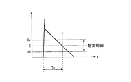
また、上記の第1実施例においては、図4に示す如く、DC−DCコンバータ10の異常有無の判定を、スイッチング素子22の強制オンの開始からスイッチング素子22に流れる電流Iが所定の基準電流値I0に達するまでの到達時間Tに基づいて行うこととしているが、本発明はこれに限定されるものではなく、スイッチング素子22の強制オン中にそのスイッチング素子22に流れる電流Iの時間変化(具体的には、増加率)に基づいて行うこととすればよく、例えば図6に示す如く、スイッチング素子22の強制オンの開始から予め定められた所定時間T0が経過した時点でのスイッチング素子22に流れる電流Iの大きさに基づいて行うこととしてもよい。
Further, in the first embodiment, as shown in FIG. 4, whether the DC-DC converter 10 is abnormal or not is determined based on whether the current I flowing from the forced on of the switching element 22 to the switching element 22 is a predetermined reference current. However, the present invention is not limited to this, and the time change of the current I flowing through the switching element 22 during the forced on of the switching element 22 ( Specifically, it may be performed based on the increase rate). For example, as shown in FIG. 6, the switching element 22 at the time when a predetermined time T0 has elapsed from the start of the forced on of the switching element 22. It is good also as performing based on the magnitude | size of the electric current I which flows into.
かかる変形例において、検査用回路44は、制御部40から検査の実行指示を受けると、スイッチング素子22を強制的にオンする指令をゲートドライバ34に対して供給すると共に、かかる強制オンの開始からの時間tをカウントする。そして、スイッチング素子22の強制オンの開始からの時間tが所定の基準時間T0に達するか否かを判別すると共に、その強制オンの開始からの時間tが所定の基準時間T0に達した場合には更に、スイッチング素子22に流れる電流Iを検出し、その検出電流Iが想定範囲内にあるか否かを判別する。
In such a modification, upon receiving an inspection execution instruction from the control unit 40, the inspection circuit 44 supplies a command for forcibly turning on the switching element 22 to the gate driver 34, and from the start of the forced on. The time t is counted. Then, it is determined whether or not the time t from the start of forced on of the switching element 22 reaches a predetermined reference time T0, and when the time t from the start of forced on reaches the predetermined reference time T0. Further, the current I flowing through the switching element 22 is detected, and it is determined whether or not the detected current I is within an assumed range.
尚、上記の所定の基準時間T0は、昇圧回路28に入力される基準となる入力電圧Viすなわちバッテリ14の基準となる出力電圧と、インダクタ20の基準となるインダクタンス値Lと、に応じた傾きで増加する電流値Iが上記の所定の基準電流値I0に達するのに要する時間であって、予め定められている。また、上記の想定範囲は、昇圧回路28の入力電圧Vi及びインダクタ20のインダクタンス値Lそれぞれの正常値であるバラツキの下限値及び上限値から求まる電流値範囲であって、予め下限値Id及び上限値Iuが定められた電流値範囲である。
The predetermined reference time T0 is a slope corresponding to the input voltage Vi serving as a reference input to the booster circuit 28, that is, the output voltage serving as the reference of the battery 14, and the inductance value L serving as the reference of the inductor 20. This is the time required for the current value I that increases in step S1 to reach the predetermined reference current value I0, and is predetermined. The above assumed range is a current value range obtained from the lower limit value and the upper limit value of the variation, which are normal values of the input voltage Vi of the booster circuit 28 and the inductance value L of the inductor 20, and is previously set to the lower limit value Id and the upper limit value. The value Iu is a defined current value range.
検査用回路44は、スイッチング素子22の強制オンの開始から所定時間T0が経過した時点でのスイッチング素子22に流れる電流Iが想定範囲内にあると判別した場合は、スイッチング素子22に流れる電流が想定内の傾きで増加していると判断して、DC−DCコンバータ10が正常状態にあると判定する。また、スイッチング素子22の強制オンの開始から所定時間T0が経過した時点でのスイッチング素子22に流れる電流Iが想定範囲の上限値Iuを上回ると判別した場合は、スイッチング素子22に流れる電流が想定を超える傾きで増加していると判断して、DC−DCコンバータ10が異常状態にあると判定する。この際の異常判定は、図3に示す異常判定Xである。更に、スイッチング素子22の強制オンの開始から所定時間T0が経過した時点でのスイッチング素子22に流れる電流Iが想定範囲の下限値Idを下回ると判別した場合は、スイッチング素子22に流れる電流が想定を下回る傾きで増加している或いは増加していないと判断して、DC−DCコンバータ10が異常状態にあると判定する。この際の異常判定は、図3に示す異常判定Yである。
When the inspection circuit 44 determines that the current I flowing through the switching element 22 at the time when the predetermined time T0 has elapsed from the start of forced on of the switching element 22 is within the assumed range, the current flowing through the switching element 22 is It is determined that the slope is increasing at the expected slope, and it is determined that the DC-DC converter 10 is in a normal state. Further, when it is determined that the current I flowing through the switching element 22 at the time when the predetermined time T0 has elapsed from the start of forced on of the switching element 22 exceeds the upper limit value Iu of the assumed range, the current flowing through the switching element 22 is assumed. And the DC-DC converter 10 is determined to be in an abnormal state. The abnormality determination at this time is the abnormality determination X shown in FIG. Further, when it is determined that the current I flowing through the switching element 22 at the time when the predetermined time T0 has elapsed from the start of forced on of the switching element 22 is below the lower limit value Id of the assumed range, the current flowing through the switching element 22 is assumed. It is determined that the DC-DC converter 10 is in an abnormal state by determining that it has increased or not increased with a slope lower than. The abnormality determination at this time is the abnormality determination Y shown in FIG.
かかる変形例においても、DC−DCコンバータ10の異常有無の判定を、昇圧回路28での昇圧動作が行われないその自動再始動時以外のタイミングで行うので、昇圧回路28に昇圧動作を行わせることなく正確に行うことが可能である。
Also in such a modification, the determination of the presence or absence of abnormality of the DC-DC converter 10 is performed at a timing other than the automatic restart when the boosting operation in the boosting circuit 28 is not performed, so that the boosting circuit 28 performs the boosting operation. It is possible to carry out accurately without any problem.
また、上記の第1実施例においては、昇圧回路28がダイオード24を用いて構成されているが、本発明はこれに限定されるものではなく、図7に示す如く、ダイオード24に代えて同期整流用の素子50を使用するものであってもよい。
In the first embodiment, the booster circuit 28 is configured using the diode 24. However, the present invention is not limited to this, and as shown in FIG. The element 50 for rectification may be used.
また、上記の第1実施例においては、スイッチング素子22に流れる電流Iを検出するのに抵抗36を用いることとしているが、本発明はこれに限定されるものではなく、図7に示す如く、抵抗36に代えて、スイッチング素子22のオン抵抗を利用してその両端電位からそのスイッチング素子22に流れる電流Iを検出することとしてもよい。
In the first embodiment, the resistor 36 is used to detect the current I flowing through the switching element 22. However, the present invention is not limited to this, and as shown in FIG. Instead of the resistor 36, the on-resistance of the switching element 22 may be used to detect the current I flowing through the switching element 22 from the potential at both ends thereof.
また、上記の第1実施例は、アイドリングストップシステム搭載車両におけるエンジンの自動再始動時にバックアップ電源確保等のために昇圧動作を行うDC−DCコンバータ10の例であるが、本発明はこれに限定されるものではなく、かかるエンジンの自動再始動時以外のタイミングに昇圧動作を行うDC−DCコンバータに適用することとしてもよく、また、車両以外の装置に搭載されるDC−DCコンバータに適用することとしてもよい。
In addition, the first embodiment is an example of the DC-DC converter 10 that performs a boosting operation for securing a backup power source or the like when the engine is automatically restarted in a vehicle equipped with an idling stop system. However, the present invention is not limited to this. However, the present invention may be applied to a DC-DC converter that performs a step-up operation at a timing other than when the engine is automatically restarted, and is also applied to a DC-DC converter mounted on a device other than a vehicle. It is good as well.
図8は、本発明の第2実施例であるDC−DCコンバータ100の異常判定装置102の要部構成図を示す。
FIG. 8 shows a configuration diagram of a main part of the abnormality determination device 102 of the DC-DC converter 100 according to the second embodiment of the present invention.
本実施例のDC−DCコンバータ100は、例えば、車両に搭載されており、高圧バッテリの出力電圧を降圧して車載電気負荷に電力供給を行う降圧装置である。DC−DCコンバータ100は、高圧バッテリ104と電気負荷106との間に介在されている。高圧バッテリ104は、蓄えている電力を所定電圧(通常は、例えば240ボルト)で外部出力することが可能な車載バッテリである。また、電気負荷106は、上記の電気負荷16と同様であってもよく、また、高圧バッテリ104の出力電圧よりも低い電圧を出力する低圧バッテリであってもよい。
The DC-DC converter 100 of the present embodiment is mounted on a vehicle, for example, and is a step-down device that steps down the output voltage of a high-voltage battery and supplies power to an on-vehicle electric load. The DC-DC converter 100 is interposed between the high voltage battery 104 and the electric load 106. The high-voltage battery 104 is an in-vehicle battery that can output stored electric power at a predetermined voltage (usually, for example, 240 volts). The electric load 106 may be the same as the electric load 16 described above, or may be a low voltage battery that outputs a voltage lower than the output voltage of the high voltage battery 104.
DC−DCコンバータ100は、スイッチング素子110と、ダイオード112と、インダクタ114と、コンデンサ116と、からなる降圧回路118を備えている。スイッチング素子110の一端は、DC−DCコンバータ100すなわち降圧回路118の入力端子として、高圧バッテリ104に接続されている。スイッチング素子110の一端には、高圧バッテリ104の電圧が入力電圧Viとして入力される。
The DC-DC converter 100 includes a step-down circuit 118 including a switching element 110, a diode 112, an inductor 114, and a capacitor 116. One end of the switching element 110 is connected to the high voltage battery 104 as an input terminal of the DC-DC converter 100, that is, the step-down circuit 118. The voltage of the high voltage battery 104 is input to one end of the switching element 110 as the input voltage Vi.
スイッチング素子110の他端には、ダイオード112のカソード端子が接続されている。ダイオード112のアノード端子は接地されている。スイッチング素子110は、高圧バッテリ104とダイオード112との間に介在されている。スイッチング素子110は、後述の降圧制御ICからの指令に従ってオン/オフされる例えばMOS−FETなどである。
The other end of the switching element 110 is connected to the cathode terminal of the diode 112. The anode terminal of the diode 112 is grounded. The switching element 110 is interposed between the high voltage battery 104 and the diode 112. The switching element 110 is, for example, a MOS-FET or the like that is turned on / off in accordance with a command from a step-down control IC described later.
スイッチング素子110の他端及びダイオード112のカソード端子には、インダクタ114の一端側が接続されている。インダクタ114は、所定のインダクタンス値Lを有するチョークコイルである。インダクタ114の他端は、コンデンサ116を介して接地されていると共に、DC−DCコンバータ100の出力端子すなわち降圧回路118として、電気負荷106に接続されている。DC−DCコンバータ100すなわち降圧回路118は、スイッチング素子110のオン/オフにより高圧バッテリ104の出力電圧を降圧して電気負荷106へ電力供給を行う。
One end of the inductor 114 is connected to the other end of the switching element 110 and the cathode terminal of the diode 112. The inductor 114 is a choke coil having a predetermined inductance value L. The other end of the inductor 114 is grounded via a capacitor 116 and is connected to the electric load 106 as an output terminal of the DC-DC converter 100, that is, a step-down circuit 118. The DC-DC converter 100, that is, the step-down circuit 118 steps down the output voltage of the high-voltage battery 104 by turning on / off the switching element 110 and supplies power to the electric load 106.
かかる降圧回路118においては、まず、スイッチング素子110がオフからオンへ切り替わると、インダクタ114、電気負荷106、及びコンデンサ116に高圧バッテリ104の電圧に基づく電圧が印加される。インダクタ114に電圧が印加されると、インダクタ114に電流が流れてそのインダクタ114が充電される。この際、インダクタ114に流れる電流は、時間の経過に伴って比例的に増加する。また、インダクタ114に電圧が印加されているので、降圧回路118の出力電圧Voすなわち電気負荷106に印加される電圧は、降圧回路118の入力電圧Viよりも低くなる。更に、コンデンサ116は、降圧回路118の出力電圧Voで充電される。
In the step-down circuit 118, first, when the switching element 110 is switched from OFF to ON, a voltage based on the voltage of the high voltage battery 104 is applied to the inductor 114, the electric load 106, and the capacitor 116. When a voltage is applied to the inductor 114, a current flows through the inductor 114 and the inductor 114 is charged. At this time, the current flowing through the inductor 114 increases proportionally with time. Since the voltage is applied to the inductor 114, the output voltage Vo of the step-down circuit 118, that is, the voltage applied to the electric load 106 is lower than the input voltage Vi of the step-down circuit 118. Further, the capacitor 116 is charged with the output voltage Vo of the step-down circuit 118.
次に、スイッチング素子110がオンからオフへ切り替わると、以後、インダクタ114に蓄えられていた電力が電気負荷106へ向けて放出されて、インダクタ114に流れる電流が時間の経過に伴って比例的に減少する。この際、降圧回路118の出力電圧Voは、コンデンサ116の両端電圧となり、降圧回路118の入力電圧Viよりも低くなる。そして、その後は、スイッチング素子110のオン/オフが所定周期で繰り返し行われる。かかる動作によれば、降圧回路118が常に入力電圧Viよりも低い電圧Voを出力するDC−DCコンバータ100による降圧が実現される。
Next, when the switching element 110 is switched from on to off, the electric power stored in the inductor 114 is released toward the electric load 106 and the current flowing through the inductor 114 is proportionally proportional to the passage of time. Decrease. At this time, the output voltage Vo of the step-down circuit 118 becomes the voltage across the capacitor 116 and is lower than the input voltage Vi of the step-down circuit 118. Thereafter, the switching element 110 is repeatedly turned on / off at a predetermined cycle. According to such an operation, step-down by the DC-DC converter 100 in which the step-down circuit 118 always outputs a voltage Vo lower than the input voltage Vi is realized.
DC−DCコンバータ100は、また、上記の如く降圧回路118での降圧動作を制御する降圧制御IC120を備えている。降圧制御IC120は、スイッチング素子110のオン/オフを制御する回路である。
The DC-DC converter 100 also includes a step-down control IC 120 that controls the step-down operation in the step-down circuit 118 as described above. The step-down control IC 120 is a circuit that controls ON / OFF of the switching element 110.
DC−DCコンバータ100において、スイッチング素子110の他端及びダイオード112のカソード端子とインダクタ114の一端との間には、抵抗122が介在されている。抵抗122は、スイッチング素子110側からインダクタ114に向けて流れる電流の大きさを検出するための電流検出抵抗である。抵抗122の両端は、降圧制御IC120に内蔵された電流検出アンプ124の入力端子に接続されている。電流検出アンプ124は、スイッチング素子110側からインダクタ114へ向けて流れる電流の大きさに応じた信号を出力するアンプである。
In the DC-DC converter 100, a resistor 122 is interposed between the other end of the switching element 110 and the cathode terminal of the diode 112 and one end of the inductor 114. The resistor 122 is a current detection resistor for detecting the magnitude of the current flowing from the switching element 110 side toward the inductor 114. Both ends of the resistor 122 are connected to input terminals of a current detection amplifier 124 built in the step-down control IC 120. The current detection amplifier 124 is an amplifier that outputs a signal corresponding to the magnitude of the current flowing from the switching element 110 side toward the inductor 114.
降圧制御IC120は、スイッチング素子110のオン/オフを制御するスイッチ制御回路128と、インダクタ114のショートやスイッチング素子110の異常などのDC−DCコンバータ100の異常を判定する検査用回路126と、を有している。スイッチ制御回路128は、スイッチング素子110のオン/オフにより降圧回路118での降圧動作を制御すると共に、また、DC−DCコンバータ100の異常有無の判定時にスイッチング素子110を強制的にオンさせることが可能である。
The step-down control IC 120 includes a switch control circuit 128 that controls ON / OFF of the switching element 110 and a test circuit 126 that determines an abnormality of the DC-DC converter 100 such as a short circuit of the inductor 114 or an abnormality of the switching element 110. Have. The switch control circuit 128 controls the step-down operation in the step-down circuit 118 by turning on / off the switching element 110 and forcibly turns on the switching element 110 when determining whether or not the DC-DC converter 100 is abnormal. Is possible.
検査用回路126には、電流検出アンプ124の出力端子が接続されている。検査用回路126は、スイッチ制御回路128によりスイッチング素子110がオンされているタイミングで、電流検出アンプ124の出力信号に基づくスイッチング素子110からインダクタ114へ向けて流れる電流に基づいてDC−DCコンバータ100の異常を判定する。
An output terminal of the current detection amplifier 124 is connected to the inspection circuit 126. The test circuit 126 is based on the current flowing from the switching element 110 to the inductor 114 based on the output signal of the current detection amplifier 124 at the timing when the switching element 110 is turned on by the switch control circuit 128. Judge abnormalities.
スイッチング素子110がオフからオンに切り替わると、以後、インダクタ114に流れる電流Iは、上記(1)式と同様に、降圧回路118の入力電圧Viと出力電圧Voとの差圧とインダクタンス値Lとスイッチング素子110のオン継続時間tとに応じた値となり、DC−DCコンバータ100が正常状態にあれば、スイッチング素子110のオン継続時間tに時間比例して一定割合で増加する。また逆に、スイッチング素子110がオンからオフに切り替わると、以後、インダクタ114に流れる電流Iは、降圧回路118の入力電圧Viと出力電圧Voとの差圧とインダクタンス値Lとスイッチング素子110のオフ継続時間tとに応じた値となり、スイッチング素子110のオフ継続時間tに時間比例して一定割合で減少する。
When the switching element 110 is switched from OFF to ON, the current I flowing through the inductor 114 thereafter is the difference between the input voltage Vi and the output voltage Vo of the step-down circuit 118, the inductance value L, and the equation (1). If the DC-DC converter 100 is in a normal state, the value increases in proportion to the ON duration time t of the switching element 110 at a constant rate. Conversely, when the switching element 110 is switched from on to off, the current I flowing through the inductor 114 thereafter is the difference between the input voltage Vi and the output voltage Vo of the step-down circuit 118, the inductance value L, and the switching element 110 being off. It becomes a value corresponding to the duration t, and decreases at a constant rate in proportion to the duration OFF of the switching element 110 in time.
この点、降圧回路118の入力電圧Vi及び出力電圧Voが安定した状態にあれば、スイッチング素子110がオン又はオフに切り替わってから、インダクタ114に流れる電流Iが予め定められた所定の基準電流値に達するまでの到達時間を測定することで、DC−DCコンバータ100の異常を判定することが可能である。上記の到達時間が想定範囲内にあれば、DC−DCコンバータ100が正常状態にあると判定し、一方、上記の到達時間が想定範囲内になければ、DC−DCコンバータ100が異常状態にあると判定することができる。
In this regard, if the input voltage Vi and the output voltage Vo of the step-down circuit 118 are stable, the current I flowing through the inductor 114 after the switching element 110 is turned on or off is a predetermined reference current value. It is possible to determine the abnormality of the DC-DC converter 100 by measuring the arrival time until reaching. If the arrival time is within the assumed range, it is determined that the DC-DC converter 100 is in a normal state. On the other hand, if the arrival time is not within the assumed range, the DC-DC converter 100 is in an abnormal state. Can be determined.
そこで、本実施例においては、上述の手法を用いてDC−DCコンバータ100の異常を判定する。降圧制御IC120の検査用回路126は、スイッチング素子110がオンされると、時間カウントを開始して、以後、かかるオンの開始からの時間をカウントする。また、検査用回路126は、電流検出アンプ124の出力信号に基づいてインダクタ114に流れる電流Iを検出し、その検出電流Iが所定の基準電流値に達するか否かを判別する。尚、この所定の基準電流値は、降圧回路118に入力される基準となる入力電圧Vi及び降圧回路118から出力される基準となる出力電圧Voと、インダクタ114の基準となるインダクタンス値Lと、スイッチング素子110のオンの開始からの基準となる時間と、から求まるインダクタ114に流れると想定される規定の電流値であって、予め定められている。
Therefore, in this embodiment, the abnormality of the DC-DC converter 100 is determined using the above-described method. When the switching element 110 is turned on, the test circuit 126 of the step-down control IC 120 starts time counting, and thereafter counts the time from the start of the ON. The inspection circuit 126 detects the current I flowing through the inductor 114 based on the output signal of the current detection amplifier 124, and determines whether or not the detected current I reaches a predetermined reference current value. The predetermined reference current value includes a reference input voltage Vi input to the step-down circuit 118, a reference output voltage Vo output from the step-down circuit 118, an inductance value L serving as a reference of the inductor 114, It is a predetermined current value that is assumed to flow through the inductor 114 obtained from the reference time from the start of turning on of the switching element 110, and is predetermined.
検査用回路126は、スイッチング素子110のオン開始からの経過時間と検出電流Iが所定の基準電流値に達するか否かの判別結果とに基づいて、スイッチング素子110のオン開始から上記の検出電流Iが所定の基準電流値に達するまでの到達時間を測定し、その到達時間が想定範囲内にあるか否かを判別する。尚、この想定範囲は、降圧回路118の入力電圧Vi及び出力電圧Vo並びにインダクタ114のインダクタンス値Lそれぞれの正常値であるバラツキの下限値及び上限値から求まる時間範囲であって、予め下限値及び上限値が定められた時間範囲である。
The inspection circuit 126 detects the above-described detection current from the on-start of the switching element 110 based on the elapsed time from the on-start of the switching element 110 and the determination result of whether or not the detection current I reaches a predetermined reference current value. The arrival time until I reaches a predetermined reference current value is measured, and it is determined whether or not the arrival time is within an assumed range. The assumed range is a time range obtained from the lower limit value and the upper limit value of the normal values of the input voltage Vi and output voltage Vo of the step-down circuit 118 and the inductance value L of the inductor 114. This is a time range in which an upper limit is set.
検査用回路126は、上記の到達時間が想定範囲内にあると判別した場合は、インダクタ114に流れる電流が想定内の傾きで増加していると判断して、DC−DCコンバータ100が正常状態にあると判定する。一方、上記の到達時間が想定範囲の下限値を下回ると判別した場合は、インダクタ114に流れる電流が想定を超える傾きで増加していると判断して、DC−DCコンバータ100に図3において異常判定Xで示す異常が生じていると判定する。また、上記の到達時間が想定範囲の上限値を上回ると判別した場合は、インダクタ114に流れる電流が想定を下回る傾きで増加している又はほとんど或いは全く増加していないと判断して、DC−DCコンバータ100に図3において異常判定Yで示す異常が生じていると判定する。
When the inspection circuit 126 determines that the arrival time is within the assumed range, the inspection circuit 126 determines that the current flowing through the inductor 114 is increasing with the expected slope, and the DC-DC converter 100 is in a normal state. It is determined that On the other hand, if it is determined that the arrival time is below the lower limit value of the assumed range, it is determined that the current flowing through the inductor 114 is increasing at a slope exceeding the expected value, and the DC-DC converter 100 is abnormal in FIG. It is determined that an abnormality indicated by determination X has occurred. Further, when it is determined that the arrival time exceeds the upper limit value of the assumed range, it is determined that the current flowing through the inductor 114 is increasing at a slope lower than expected, or hardly or not at all, and DC− It is determined that the abnormality indicated by the abnormality determination Y in FIG.
このように、本実施例の異常判定装置102においては、スイッチング素子110のオン中にそのオン開始からインダクタ114に流れる電流Iが所定の基準電流値に達するまでの到達時間を測定し、その到達時間が想定範囲内にあるか否かに基づいてDC−DCコンバータ100の異常有無を判定することができる。上記の到達時間が想定範囲内にある場合は、DC−DCコンバータ100が正常状態にあると判定し、一方、上記の到達時間が想定範囲外にある場合は、DC−DCコンバータ100が異常状態にあると判定することができる。
As described above, in the abnormality determination device 102 according to the present embodiment, when the switching element 110 is turned on, the arrival time from when the switching element 110 is turned on until the current I flowing through the inductor 114 reaches a predetermined reference current value is measured. Whether or not the DC-DC converter 100 is abnormal can be determined based on whether or not the time is within an assumed range. When the arrival time is within the assumed range, it is determined that the DC-DC converter 100 is in a normal state. On the other hand, when the arrival time is outside the assumed range, the DC-DC converter 100 is in an abnormal state. It can be determined that
従って、本実施例において、DC−DCコンバータ100の異常有無の判定は、降圧回路118での降圧動作が行われるタイミングに限定されて行われるものではなく、降圧回路118内のスイッチング素子110を強制的にオンすることでも行われる。このため、本実施例の異常判定装置102によれば、DC−DCコンバータ100の異常有無の判定を、降圧回路118に降圧動作を行わせることなく正確に行うことが可能である。
Therefore, in this embodiment, the determination of whether the DC-DC converter 100 is abnormal is not limited to the timing at which the step-down operation in the step-down circuit 118 is performed, and the switching element 110 in the step-down circuit 118 is forced. It is also done by turning on automatically. Therefore, according to the abnormality determination device 102 of the present embodiment, it is possible to accurately determine whether the DC-DC converter 100 is abnormal without causing the step-down circuit 118 to perform a step-down operation.
尚、上記の第2実施例においては、スイッチ制御回路128がスイッチング素子110をオンさせることにより特許請求の範囲に記載した「オン/オフ制御手段」及び「第1のステップ」が、検査用回路126がスイッチング素子110のオン中に電流検出アンプ124の出力信号に基づいてインダクタ114に流れる電流Iを検出することにより特許請求の範囲に記載した「電流検出手段」が、検査用回路126がスイッチング素子110のオン中にそのオン開始からインダクタ114に流れる電流Iが所定の基準電流値に達するまでの到達時間に基づいてDC−DCコンバータ100の異常有無を判定することにより特許請求の範囲に記載した「異常判定手段」及び「第2のステップ」が、それぞれ実現されている。
In the second embodiment, when the switch control circuit 128 turns on the switching element 110, the "on / off control means" and the "first step" described in the claims are the circuit for inspection. 126 detects the current I flowing through the inductor 114 based on the output signal of the current detection amplifier 124 while the switching element 110 is on, so that the “current detection means” described in the claims is switched by the test circuit 126. Claims are made by determining whether the DC-DC converter 100 is abnormal based on the arrival time from when the element 110 is turned on until the current I flowing through the inductor 114 reaches a predetermined reference current value. The “abnormality determination means” and the “second step” are realized.
ところで、上記の第2実施例においては、DC−DCコンバータ100の異常有無の判定を、スイッチング素子110のオン開始からインダクタ114に流れる電流Iが所定の基準電流値に達するまでの到達時間に基づいて行うこととしているが、本発明はこれに限定されるものではなく、スイッチング素子110のオン中にインダクタ114に流れる電流Iの時間変化(具体的には、増加率)に基づいて行うこととすればよく、スイッチング素子110のオン開始から予め定められた所定時間が経過した時点でのインダクタ114に流れる電流Iの大きさに基づいて行うこととしてもよい。
By the way, in the second embodiment, whether the DC-DC converter 100 is abnormal is determined based on the arrival time from when the switching element 110 is turned on until the current I flowing through the inductor 114 reaches a predetermined reference current value. However, the present invention is not limited to this, and is performed based on a change over time (specifically, an increase rate) of the current I flowing through the inductor 114 while the switching element 110 is on. What is necessary is just to carry out based on the magnitude | size of the electric current I which flows into the inductor 114 at the time of the predetermined time having passed since the ON start of the switching element 110 passed.
かかる変形例において、検査用回路126は、スイッチング素子110がオンされると、時間カウントを開始して、以後、かかるオンの開始からの時間をカウントする。そして、スイッチング素子110のオン開始からの時間が所定の基準時間に達するか否かを判別すると共に、そのオン開始からの時間が所定の基準時間に達した場合には更に、インダクタ114に流れる電流Iを検出し、その検出電流Iが想定範囲内にあるか否かを判別する。尚、上記の所定の基準時間は、降圧回路118に入力される基準となる入力電圧Vi及び降圧回路118から出力される基準となる出力電圧Voと、インダクタ114の基準となるインダクタンス値Lと、に応じた傾きで増加する電流値Iが上記の所定の基準電流値に達するのに要する時間であって、予め定められている。また、上記の想定範囲は、降圧回路118の入力電圧Vi及び出力電圧Vo並びにインダクタ114のインダクタンス値Lそれぞれの正常値であるバラツキの下限値及び上限値から求まる電流値範囲であって、予め下限値及び上限値が定められた電流値範囲である。
In such a modification, the inspection circuit 126 starts time counting when the switching element 110 is turned on, and thereafter counts time from the start of such on. Then, it is determined whether or not the time from the on start of the switching element 110 reaches a predetermined reference time. When the time from the on start of the switching element 110 reaches the predetermined reference time, the current flowing in the inductor 114 is further increased. I is detected, and it is determined whether or not the detected current I is within an assumed range. The predetermined reference time includes the input voltage Vi serving as a reference input to the step-down circuit 118, the output voltage Vo serving as a reference output from the step-down circuit 118, the inductance value L serving as a reference of the inductor 114, The time required for the current value I increasing at a slope corresponding to the above to reach the predetermined reference current value is predetermined. Further, the above assumed range is a current value range obtained from the lower limit value and the upper limit value of the variation, which are normal values of the input voltage Vi and output voltage Vo of the step-down circuit 118 and the inductance value L of the inductor 114. This is a current value range in which a value and an upper limit value are determined.
検査用回路126は、スイッチング素子110のオン開始から所定時間が経過した時点でのインダクタ114に流れる電流Iが想定範囲内にあると判別した場合は、インダクタ114に流れる電流が想定内の傾きで増加していると判断して、DC−DCコンバータ100が正常状態にあると判定する。また、スイッチング素子110のオン開始から所定時間が経過した時点でのインダクタ114に流れる電流Iが想定範囲の上限値を上回ると判別した場合は、インダクタ114に流れる電流が想定を超える傾きで増加していると判断して、DC−DCコンバータ100に図3において異常判定Xで示す異常が生じていると判定する。更に、スイッチング素子110のオン開始から所定時間が経過した時点でのインダクタ114に流れる電流Iが想定範囲の下限値を下回ると判別した場合は、インダクタ114に流れる電流が想定を下回る傾きで増加している又はほとんど或いは全く増加していないと判断して、DC−DCコンバータ100に図3において異常判定Yで示す異常が生じていると判定する。かかる変形例においても、DC−DCコンバータ100の異常有無の判定を、降圧回路118での降圧動作が行われないタイミングでも行うことが可能であるので、降圧回路118に降圧動作を行わせることなく正確に行うことが可能である。
When the inspection circuit 126 determines that the current I flowing through the inductor 114 at the time when a predetermined time has elapsed from the start of turning on of the switching element 110 is within the assumed range, the current flowing through the inductor 114 has an assumed inclination. It is determined that the number has increased, and it is determined that the DC-DC converter 100 is in a normal state. In addition, when it is determined that the current I flowing through the inductor 114 at the time when a predetermined time has elapsed from the start of turning on of the switching element 110 exceeds the upper limit value of the assumed range, the current flowing through the inductor 114 increases with a slope exceeding the assumption. It is determined that the abnormality indicated by abnormality determination X in FIG. 3 has occurred in the DC-DC converter 100. Furthermore, when it is determined that the current I flowing through the inductor 114 at the time when a predetermined time has elapsed from the start of turning on of the switching element 110 falls below the lower limit value of the assumed range, the current flowing through the inductor 114 increases with a slope lower than expected. 3, it is determined that the abnormality indicated by the abnormality determination Y in FIG. 3 has occurred in the DC-DC converter 100. Also in such a modification, it is possible to determine whether or not the DC-DC converter 100 is abnormal even at a timing when the step-down operation in the step-down circuit 118 is not performed, so that the step-down circuit 118 does not perform the step-down operation. It can be done accurately.
また、上記の第2実施例においては、検査用回路126がスイッチング素子110からインダクタ114へ向けて流れる電流に基づいてDC−DCコンバータ100の異常を判定するタイミングを、スイッチング素子110がオンされている期間中としているが、そのスイッチング素子110がオフされている期間中としてもよい。かかる変形例においては、DC−DCコンバータ100の異常有無の判定を、スイッチング素子110のオフ中にインダクタ114に流れる電流Iの時間変化(具体的には、減少率)に基づいて行うこととすればよい。すなわち、スイッチング素子110のオフ中にそのオフ開始からインダクタ114に流れる電流Iが所定の基準電流値に低下するまでの到達時間を測定し、その到達時間が想定範囲内にあるか否かに基づいてDC−DCコンバータ100の異常有無を判定すること、或いは、スイッチング素子110のオフ開始から予め定められた所定時間が経過した時点でのインダクタ114に流れる電流Iの大きさに基づいてDC−DCコンバータ100の異常有無を判定することとすればよい。
Further, in the second embodiment, the timing at which the inspection circuit 126 determines the abnormality of the DC-DC converter 100 based on the current flowing from the switching element 110 to the inductor 114 is turned on. However, the switching element 110 may be turned off. In such a modification, the determination of the presence or absence of abnormality of the DC-DC converter 100 is made based on the temporal change (specifically, the reduction rate) of the current I flowing through the inductor 114 while the switching element 110 is off. That's fine. That is, when the switching element 110 is turned off, the arrival time from when the switching element 110 is turned off until the current I flowing through the inductor 114 decreases to a predetermined reference current value is measured, and based on whether the arrival time is within the assumed range. Whether the DC-DC converter 100 is abnormal or not, or based on the magnitude of the current I flowing through the inductor 114 when a predetermined time elapses after the switching element 110 is turned off. What is necessary is just to determine the presence or absence of abnormality of the converter 100.
また、上記の第2実施例においては、降圧回路118がダイオード112を用いて構成されているが、本発明はこれに限定されるものではなく、ダイオード112に代えて同期整流用の素子を使用するものであってもよい。
In the second embodiment, the step-down circuit 118 is configured by using the diode 112. However, the present invention is not limited to this, and an element for synchronous rectification is used instead of the diode 112. You may do.
図9は、本発明の第3実施例であるDC−DCコンバータ200の異常判定装置202の要部構成図を示す。尚、図9において、上記図8と同様の構成を示す部分については、同一の符号を付してその説明を省略又は簡略する。
FIG. 9 shows a configuration diagram of a main part of the abnormality determination device 202 of the DC-DC converter 200 according to the third embodiment of the present invention. In FIG. 9, portions having the same configuration as in FIG. 8 are given the same reference numerals, and description thereof is omitted or simplified.
本実施例のDC−DCコンバータ200は、例えば、車両に搭載されており、高圧バッテリの出力電圧を降圧して車載電気負荷に電力供給を行う降圧装置である。DC−DCコンバータ200は、高圧バッテリ104と電気負荷106との間に介在されている。DC−DCコンバータ200は、2つのスイッチング素子202,204と、インダクタ206と、コンデンサ208と、からなる降圧回路210を備えている。
The DC-DC converter 200 of the present embodiment is mounted on a vehicle, for example, and is a step-down device that steps down the output voltage of a high-voltage battery and supplies power to an on-vehicle electric load. The DC-DC converter 200 is interposed between the high voltage battery 104 and the electric load 106. The DC-DC converter 200 includes a step-down circuit 210 including two switching elements 202 and 204, an inductor 206, and a capacitor 208.
高圧バッテリ104と接地端との間には、両スイッチング素子202,204が直列接続されている。すなわち、スイッチング素子202の一端は、DC−DCコンバータ200すなわち降圧回路210の入力端子として、高圧バッテリ104に接続されている。スイッチング素子202の一端には、高圧バッテリ104の電圧が入力電圧Viとして入力される。スイッチング素子202の他端には、スイッチング素子204の一端が接続されている。スイッチング素子204の他端は、接地端側に接続されている。両スイッチング素子202,204は、後述の降圧制御ICからの指令に従ってオン/オフされる例えばMOS−FETなどである。
The switching elements 202 and 204 are connected in series between the high voltage battery 104 and the ground terminal. That is, one end of the switching element 202 is connected to the high voltage battery 104 as an input terminal of the DC-DC converter 200, that is, the step-down circuit 210. The voltage of the high voltage battery 104 is input to one end of the switching element 202 as the input voltage Vi. One end of the switching element 204 is connected to the other end of the switching element 202. The other end of the switching element 204 is connected to the ground end side. Both switching elements 202 and 204 are, for example, MOS-FETs that are turned on / off in accordance with a command from a step-down control IC described later.
スイッチング素子202の他端及びスイッチング素子204の一端には、インダクタ206の一端側が接続されている。インダクタ206は、所定のインダクタンス値Lを有するチョークコイルである。インダクタ206の他端は、コンデンサ208を介して接地されていると共に、DC−DCコンバータ200の出力端子すなわち降圧回路210として、電気負荷106に接続されている。DC−DCコンバータ200すなわち降圧回路210は、スイッチング素子202,204のオン/オフにより高圧バッテリ104の出力電圧を降圧して電気負荷106へ電力供給を行う。
One end of an inductor 206 is connected to the other end of the switching element 202 and one end of the switching element 204. The inductor 206 is a choke coil having a predetermined inductance value L. The other end of the inductor 206 is grounded via a capacitor 208 and is connected to the electric load 106 as an output terminal of the DC-DC converter 200, that is, a step-down circuit 210. The DC-DC converter 200, that is, the step-down circuit 210 steps down the output voltage of the high-voltage battery 104 by turning on / off the switching elements 202 and 204 and supplies power to the electric load 106.
かかる降圧回路210においては、まず、スイッチング素子202がオフからオンへ切り替わりかつスイッチング素子204がオフされると、インダクタ206、電気負荷106、及びコンデンサ208に高圧バッテリ104の電圧に基づく電圧が印加される。インダクタ206に電圧が印加されると、インダクタ206に電流が流れてそのインダクタ206が充電される。この際、インダクタ206に流れる電流は、時間の経過に伴って比例的に増加する。また、インダクタ206に電圧が印加されているので、降圧回路210の出力電圧Voすなわち電気負荷106に印加される電圧は、降圧回路210の入力電圧Viよりも低くなる。更に、コンデンサ208は、降圧回路210の出力電圧Voで充電される。
In the step-down circuit 210, first, when the switching element 202 is switched from OFF to ON and the switching element 204 is turned OFF, a voltage based on the voltage of the high voltage battery 104 is applied to the inductor 206, the electric load 106, and the capacitor 208. The When a voltage is applied to the inductor 206, a current flows through the inductor 206 and the inductor 206 is charged. At this time, the current flowing through the inductor 206 increases proportionally with time. Since the voltage is applied to the inductor 206, the output voltage Vo of the step-down circuit 210, that is, the voltage applied to the electric load 106 is lower than the input voltage Vi of the step-down circuit 210. Further, the capacitor 208 is charged with the output voltage Vo of the step-down circuit 210.
次に、スイッチング素子202がオンからオフへ切り替わりかつスイッチング素子204がオフからオンへ切り替わると、以後、インダクタ206に蓄えられていた電力が電気負荷106へ向けて放出されて、インダクタ206に流れる電流が時間の経過に伴って比例的に減少する。この際、降圧回路210の出力電圧Voは、コンデンサ208の両端電圧となり、降圧回路210の入力電圧Viよりも低くなる。そして、その後は、スイッチング素子202,204のオン/オフが所定周期で繰り返し行われる。かかる動作によれば、降圧回路210が常に入力電圧Viよりも低い電圧Voを出力するDC−DCコンバータ200による降圧が実現される。
Next, when the switching element 202 is switched from on to off and the switching element 204 is switched from off to on, the electric power stored in the inductor 206 is discharged toward the electric load 106 and the current flowing through the inductor 206 is subsequently transferred. Decreases proportionally over time. At this time, the output voltage Vo of the step-down circuit 210 becomes the voltage across the capacitor 208 and is lower than the input voltage Vi of the step-down circuit 210. Thereafter, the switching elements 202 and 204 are repeatedly turned on / off at a predetermined cycle. According to such an operation, step-down by the DC-DC converter 200 in which the step-down circuit 210 always outputs a voltage Vo lower than the input voltage Vi is realized.
DC−DCコンバータ200は、また、上記の如く降圧回路210での降圧動作を制御する降圧制御IC212を備えている。降圧制御IC212は、スイッチング素子202,204のオン/オフを制御する回路である。
The DC-DC converter 200 also includes a step-down control IC 212 that controls the step-down operation in the step-down circuit 210 as described above. The step-down control IC 212 is a circuit that controls ON / OFF of the switching elements 202 and 204.
DC−DCコンバータ200において、スイッチング素子204の他端及びインダクタ206の一端と接地端との間には、抵抗214が介在されている。抵抗214は、接地端側からスイッチング素子204に向けて流れる電流の大きさを検出するための電流検出抵抗である。抵抗214の両端は、降圧制御IC212に内蔵された電流検出アンプ216の入力端子に接続されている。電流検出アンプ216は、接地端側からスイッチング素子204へ向けて流れる電流の大きさに応じた信号を出力するアンプである。降圧制御IC212は、電流検出アンプ216の出力信号に基づいて接地端側からスイッチング素子204へ向けて流れる電流Iを検出する。
In the DC-DC converter 200, a resistor 214 is interposed between the other end of the switching element 204 and one end of the inductor 206 and the ground end. The resistor 214 is a current detection resistor for detecting the magnitude of current flowing from the ground end side toward the switching element 204. Both ends of the resistor 214 are connected to input terminals of a current detection amplifier 216 built in the step-down control IC 212. The current detection amplifier 216 is an amplifier that outputs a signal corresponding to the magnitude of the current flowing from the ground end side toward the switching element 204. The step-down control IC 212 detects the current I flowing from the ground end side toward the switching element 204 based on the output signal of the current detection amplifier 216.
降圧制御IC212は、スイッチング素子202,204それぞれのオン/オフを制御するスイッチ制御回路218と、インダクタ206のショートやスイッチング素子202,204の異常などのDC−DCコンバータ200の異常有無を判定する検査用回路220と、を有している。スイッチ制御回路218は、スイッチング素子202,204のオン/オフにより降圧回路210での降圧動作を制御する。スイッチ制御回路218は、降圧回路210での降圧動作中、スイッチング素子202,204のオン/オフを、電流検出アンプ216の出力信号に基づいて検出される接地端側からスイッチング素子204へ向けて流れる電流Iに基づいてフィードバック制御する。
The step-down control IC 212 and a switch control circuit 218 for controlling on / off of each of the switching elements 202 and 204, and a test for determining whether the DC-DC converter 200 is abnormal such as a short circuit of the inductor 206 or an abnormality of the switching elements 202 and 204. Circuit 220. The switch control circuit 218 controls the step-down operation in the step-down circuit 210 by turning on / off the switching elements 202 and 204. During the step-down operation of the step-down circuit 210, the switch control circuit 218 flows ON / OFF of the switching elements 202 and 204 from the ground end side detected based on the output signal of the current detection amplifier 216 toward the switching element 204. Feedback control is performed based on the current I.
また、検査用回路220は、スイッチ制御回路218によりスイッチング素子202がオフされかつスイッチング素子204がオンされているタイミングで、電流検出アンプ216の出力信号に基づく接地端側からスイッチング素子204へ向けて流れる電流に基づいてDC−DCコンバータ200の異常を判定する。
Further, the inspection circuit 220 is directed from the ground end side based on the output signal of the current detection amplifier 216 toward the switching element 204 at a timing when the switching element 202 is turned off and the switching element 204 is turned on by the switch control circuit 218. The abnormality of the DC-DC converter 200 is determined based on the flowing current.
スイッチング素子202がオフされかつスイッチング素子204がオンされると、インダクタ206に流れる電流は、略ゼロである状態からサージ電圧に起因して大電流となり、その後は、時間の経過に伴って比例的に減少する。このインダクタ206に流れる電流Iは、降圧回路210の入力電圧Viと出力電圧Voとの差圧とインダクタンス値Lとスイッチング素子204のオン継続時間tとに応じた値となり、DC−DCコンバータ200が正常状態にあれば、スイッチング素子204のオン継続時間tに時間比例して一定割合で減少する。
When the switching element 202 is turned off and the switching element 204 is turned on, the current flowing through the inductor 206 becomes a large current due to a surge voltage from a substantially zero state, and thereafter proportional to the passage of time. To decrease. The current I flowing through the inductor 206 becomes a value according to the differential pressure between the input voltage Vi and the output voltage Vo of the step-down circuit 210, the inductance value L, and the ON duration t of the switching element 204, and the DC-DC converter 200 If in the normal state, the switching element 204 decreases at a constant rate in proportion to the ON duration t of the switching element 204.
この点、降圧回路210の入力電圧Vi及び出力電圧Voが安定した状態にあれば、スイッチング素子202がオフされかつスイッチング素子204がオンされてから、インダクタ206に流れる電流Iが予め定められた所定の基準電流値に達する(低下する)までの到達時間を測定することで、DC−DCコンバータ200の異常を判定することが可能である。上記の到達時間が想定範囲内にあれば、DC−DCコンバータ200が正常状態にあると判定し、一方、上記の到達時間が想定範囲内になければ、DC−DCコンバータ200が異常状態にあると判定することができる。
In this regard, if the input voltage Vi and output voltage Vo of the step-down circuit 210 are stable, the current I flowing through the inductor 206 is predetermined after the switching element 202 is turned off and the switching element 204 is turned on. It is possible to determine the abnormality of the DC-DC converter 200 by measuring the arrival time until the reference current value is reached (decreased). If the arrival time is within the assumed range, it is determined that the DC-DC converter 200 is in a normal state. On the other hand, if the arrival time is not within the assumed range, the DC-DC converter 200 is in an abnormal state. Can be determined.
そこで、本実施例においては、上述の手法を用いてDC−DCコンバータ200の異常を判定する。降圧制御IC212の検査用回路220は、スイッチング素子202がオフされかつスイッチング素子204がオンされると、時間カウントを開始して、以後、かかるオンの開始からの時間をカウントすると共に、電流検出アンプ216の出力信号に基づいて接地側からスイッチング素子204に流れる電流Iを検出し、その検出電流Iが所定の基準電流値I0に達する(低下する)か否かを判別する。尚、この所定の基準電流値I0は、降圧回路210に入力される基準となる入力電圧Vi及び降圧回路210から出力される基準となる出力電圧Voと、インダクタ206の基準となるインダクタンス値Lと、スイッチング素子204のオン開始からの基準となる時間と、から求まるインダクタ206に流れると想定される規定の電流値であって、予め定められている。
Therefore, in this embodiment, the abnormality of the DC-DC converter 200 is determined using the above-described method. When the switching element 202 is turned off and the switching element 204 is turned on, the test circuit 220 of the step-down control IC 212 starts time counting, and thereafter counts the time from the start of the on, and also detects a current detection amplifier. Based on the output signal 216, the current I flowing from the ground side to the switching element 204 is detected, and it is determined whether or not the detected current I reaches (decreases) a predetermined reference current value I0. The predetermined reference current value I0 includes a reference input voltage Vi input to the step-down circuit 210, an output voltage Vo which is a reference output from the step-down circuit 210, and an inductance value L which is a reference of the inductor 206. The standard current value that is assumed to flow through the inductor 206, which is obtained from the reference time from the start of turning on of the switching element 204, is determined in advance.
検査用回路220は、スイッチング素子204のオン開始からの経過時間と検出電流Iが所定の基準電流値I0に達するか否かの判別結果とに基づいて、スイッチング素子204のオン開始から上記の検出電流Iが所定の基準電流値I0に達するまでの到達時間Tを測定し、その到達時間Tが想定範囲内にあるか否かを判別する。尚、この想定範囲は、降圧回路210の入力電圧Vi及び出力電圧Vo並びにインダクタ206のインダクタンス値Lそれぞれの正常値であるバラツキの下限値及び上限値から求まる時間範囲であって、予め下限値Td及び上限値Tuが定められた時間範囲である。
The inspection circuit 220 detects the above-described detection from the start of turning on of the switching element 204 based on the elapsed time from the start of turning on of the switching element 204 and the determination result of whether or not the detected current I reaches a predetermined reference current value I0. The arrival time T until the current I reaches a predetermined reference current value I0 is measured, and it is determined whether or not the arrival time T is within the assumed range. This assumed range is a time range obtained from the lower limit value and the upper limit value of the normal values of the input voltage Vi and output voltage Vo of the step-down circuit 210 and the inductance value L of the inductor 206, and is previously set to the lower limit value Td. And an upper limit value Tu is a predetermined time range.
検査用回路220は、上記の到達時間Tが想定範囲内にあると判別した場合は、インダクタ206に流れる電流が想定内の傾きで減少していると判断して、DC−DCコンバータ200が正常状態にあると判定する。一方、上記の到達時間Tが想定範囲の下限値を下回ると判別した場合は、インダクタ206に流れる電流が想定を超える傾きで減少していると判断して、DC−DCコンバータ200に図3において異常判定Xで示す異常が生じていると判定する。また、上記の到達時間Tが想定範囲の上限値を上回ると判別した場合は、インダクタ206に流れる電流が想定を下回る傾きで減少している又はほとんど或いは全く減少していないと判断して、DC−DCコンバータ200に図3において異常判定Yで示す異常が生じていると判定する。
If the test circuit 220 determines that the arrival time T is within the assumed range, the test circuit 220 determines that the current flowing through the inductor 206 is decreasing with the expected slope, and the DC-DC converter 200 is normal. It is determined that it is in a state. On the other hand, if it is determined that the above arrival time T is below the lower limit value of the assumed range, it is determined that the current flowing through the inductor 206 is decreasing with a slope exceeding the assumed value, and the DC-DC converter 200 in FIG. It is determined that the abnormality indicated by the abnormality determination X has occurred. When it is determined that the arrival time T exceeds the upper limit value of the assumed range, it is determined that the current flowing through the inductor 206 is decreasing with a slope lower than expected, or hardly or not at all. -It is determined that the abnormality indicated by the abnormality determination Y in FIG.
このように、本実施例の異常判定装置202においては、スイッチング素子204のオン中にそのオン開始からインダクタ206に流れる電流Iが所定の基準電流値I0に達するまでの到達時間Tを測定し、その到達時間Tが想定範囲内にあるか否かに基づいてDC−DCコンバータ200の異常有無を判定することができる。上記の到達時間Tが想定範囲内にある場合は、DC−DCコンバータ200が正常状態にあると判定し、一方、上記の到達時間Tが想定範囲外にある場合は、DC−DCコンバータ200が異常状態にあると判定することができる。
As described above, in the abnormality determination device 202 of the present embodiment, the arrival time T from when the switching element 204 is turned on until the current I flowing through the inductor 206 reaches the predetermined reference current value I0 is measured. Whether or not the DC-DC converter 200 is abnormal can be determined based on whether or not the arrival time T is within an assumed range. When the arrival time T is within the assumed range, it is determined that the DC-DC converter 200 is in a normal state. On the other hand, when the arrival time T is outside the assumed range, the DC-DC converter 200 is It can be determined that the state is abnormal.
従って、本実施例において、DC−DCコンバータ200の異常有無の判定は、降圧回路210での降圧動作が行われるタイミングに限定されて行われるものではなく、降圧回路210内のスイッチング素子202のオフ及びスイッチング素子204のオンを強制的に行うことでも行われる。このため、本実施例の異常判定装置202によれば、DC−DCコンバータ200の異常有無の判定を、降圧回路210に降圧動作を行わせることなく正確に行うことが可能である。
Therefore, in this embodiment, the determination of the presence or absence of abnormality of the DC-DC converter 200 is not limited to the timing at which the step-down operation in the step-down circuit 210 is performed, but the switching element 202 in the step-down circuit 210 is turned off. The switching element 204 is also forcibly turned on. Therefore, according to the abnormality determination device 202 of this embodiment, it is possible to accurately determine whether the DC-DC converter 200 is abnormal without causing the step-down circuit 210 to perform a step-down operation.
尚、上記の第3実施例においては、スイッチ制御回路218がスイッチング素子202をオンさせかつスイッチング素子204をオンさせることにより特許請求の範囲に記載した「オン/オフ制御手段」及び「第1のステップ」が、検査用回路220がスイッチング素子204のオン中に電流検出アンプ216の出力信号に基づいてインダクタ206に流れる電流Iを検出することにより特許請求の範囲に記載した「電流検出手段」が、検査用回路220がスイッチング素子204のオン中にそのオン開始からインダクタ206に流れる電流Iが所定の基準電流値I0に達するまでの到達時間Tに基づいてDC−DCコンバータ200の異常有無を判定することにより特許請求の範囲に記載した「異常判定手段」及び「第2のステップ」が、それぞれ実現されている。
In the third embodiment described above, the switch control circuit 218 turns on the switching element 202 and turns on the switching element 204 so that the “on / off control means” and “first” The “step” detects the current I flowing in the inductor 206 based on the output signal of the current detection amplifier 216 while the switching element 204 is turned on, whereby the “current detection means” described in the claims is When the switching circuit 204 is turned on, the test circuit 220 determines whether the DC-DC converter 200 is abnormal based on the arrival time T from when the switching element 204 starts to the current I flowing through the inductor 206 reaches a predetermined reference current value I0. By doing so, the “abnormality determination means” and the “second step” described in the claims are: They are respectively realized.
ところで、上記の第3実施例においては、スイッチング素子204のオン開始からインダクタ206に流れる電流Iが所定の基準電流値I0に達するまでの到達時間Tに基づいてDC−DCコンバータ200の異常有無を判定するが、その異常有無の判定或いはインダクタ206に流れる電流Iが所定の基準電流値I0に達するか否かの判別を、スイッチング素子204のオン開始から所定時間(図10に示す時間T´)が経過するまでの期間は行わないこと、すなわち、スイッチング素子204のオン開始から所定時間(図4に示す時間T´)内を除いて行うこととしてもよい。
By the way, in the third embodiment, whether the DC-DC converter 200 is abnormal or not is determined based on the arrival time T from when the switching element 204 is turned on until the current I flowing through the inductor 206 reaches a predetermined reference current value I0. Whether or not there is an abnormality or whether or not the current I flowing through the inductor 206 reaches a predetermined reference current value I0 is determined for a predetermined time (time T ′ shown in FIG. 10) after the switching element 204 is turned on. It is also possible not to perform the period until elapse of time, that is, to perform the period excluding a predetermined time (time T ′ shown in FIG. 4) from the start of turning on of the switching element 204.
一般に、スイッチング素子204がオフからオンへ切り替わった際に発生するサージ電圧はインダクタ206に流れる電流Iに影響を及ぼすが、これに対して、上記の変形例によれば、スイッチング素子204のオン直後にDC−DCコンバータ200の異常有無の判定或いはインダクタ206に流れる電流Iが所定の基準電流値I0に達するか否かの判別を行わないので、スイッチング素子204のオフからオンへの切り替えに伴うサージ電圧に起因してDC−DCコンバータ200が異常状態であると誤判定されるのを防止することが可能である。
In general, the surge voltage generated when the switching element 204 is switched from OFF to ON affects the current I flowing through the inductor 206. On the other hand, according to the above modification, immediately after the switching element 204 is turned on. In this case, it is not determined whether the DC-DC converter 200 is abnormal or whether the current I flowing through the inductor 206 reaches a predetermined reference current value I0. It is possible to prevent the DC-DC converter 200 from being erroneously determined to be in an abnormal state due to the voltage.
また、上記の第3実施例においては、図10に示す如く、DC−DCコンバータ200の異常有無の判定を、スイッチング素子204のオン開始からインダクタ206に流れる電流Iが所定の基準電流値I0に達する(低下する)までの到達時間Tに基づいて行うこととしているが、本発明はこれに限定されるものではなく、スイッチング素子204のオン中にインダクタ206に流れる電流Iの時間変化(具体的には、減少率)に基づいて行うこととすればよく、図11に示す如く、スイッチング素子204のオン開始から予め定められた所定時間T0が経過した時点でのインダクタ206に流れる電流Iの大きさに基づいて行うこととしてもよい。
Further, in the third embodiment, as shown in FIG. 10, whether or not the DC-DC converter 200 is abnormal is determined based on whether the current I flowing through the inductor 206 from the start of turning on of the switching element 204 becomes a predetermined reference current value I0. However, the present invention is not limited to this, and the time change (specifically, the current I flowing through the inductor 206 while the switching element 204 is on) is limited to this. 11 may be performed based on the decrease rate). As shown in FIG. 11, the magnitude of the current I flowing through the inductor 206 at the time when a predetermined time T0 has elapsed from the start of turning on of the switching element 204. It is good also as based on this.
かかる変形例において、検査用回路220は、スイッチング素子202がオフされかつスイッチング素子204がオンされると、時間カウントを開始して、以後、かかるスイッチング素子204のオン開始からの時間をカウントする。そして、スイッチング素子204のオン開始からの時間が所定の基準時間に達するか否かを判別すると共に、そのオン開始からの時間が所定の基準時間に達した場合には更に、インダクタ206に流れる電流Iを検出し、その検出電流Iが想定範囲内にあるか否かを判別する。尚、上記の所定の基準時間は、降圧回路210に入力される基準となる入力電圧Vi及び降圧回路210から出力される基準となる出力電圧Voと、インダクタ206の基準となるインダクタンス値Lと、に応じた傾きで減少する電流値Iが上記の所定の基準電流値に達する(低下する)のに要する時間であって、予め定められている。また、上記の想定範囲は、降圧回路210の入力電圧Vi及び出力電圧Vo並びにインダクタ206のインダクタンス値Lそれぞれの正常値であるバラツキの下限値及び上限値から求まる電流値範囲であって、予め下限値及び上限値が定められた電流値範囲である。
In such a modification, the inspection circuit 220 starts time counting when the switching element 202 is turned off and the switching element 204 is turned on, and thereafter counts the time from the start of turning on of the switching element 204. Then, it is determined whether or not the time from the start of turning on of the switching element 204 reaches a predetermined reference time. When the time from the start of turning on reaches the predetermined reference time, the current flowing through the inductor 206 is further increased. I is detected, and it is determined whether or not the detected current I is within an assumed range. The predetermined reference time includes the reference input voltage Vi input to the step-down circuit 210, the output voltage Vo that is the reference output from the step-down circuit 210, the inductance value L that is the reference of the inductor 206, Is a time required for the current value I decreasing at a slope corresponding to the above to reach (decrease) the predetermined reference current value, and is predetermined. The above assumed range is a current value range obtained from the lower limit value and the upper limit value of the variations, which are normal values of the input voltage Vi and output voltage Vo of the step-down circuit 210 and the inductance value L of the inductor 206, and is previously set to the lower limit value. This is a current value range in which a value and an upper limit value are determined.
検査用回路220は、スイッチング素子204のオン開始から所定時間が経過した時点でのインダクタ206に流れる電流Iが想定範囲内にあると判別した場合は、インダクタ206に流れる電流が想定内の傾きで減少していると判断して、DC−DCコンバータ200が正常状態にあると判定する。また、スイッチング素子204のオン開始から所定時間が経過した時点でのインダクタ206に流れる電流Iが想定範囲の上限値を上回ると判別した場合は、インダクタ206に流れる電流が想定を超える傾きで減少していると判断して、DC−DCコンバータ200に図3において異常判定Xで示す異常が生じていると判定する。更に、スイッチング素子204のオン開始から所定時間が経過した時点でのインダクタ206に流れる電流Iが想定範囲の下限値を下回ると判別した場合は、インダクタ206に流れる電流が想定を下回る傾きで減少している又はほとんど或いは全く減少していないと判断して、DC−DCコンバータ200に図3において異常判定Yで示す異常が生じていると判定する。かかる変形例においても、DC−DCコンバータ200の異常有無の判定を、降圧回路210での降圧動作が行われないタイミングでも行うことが可能であるので、降圧回路210に降圧動作を行わせることなく正確に行うことが可能である。
When the inspection circuit 220 determines that the current I flowing through the inductor 206 at the time when a predetermined time has elapsed from the start of turning on of the switching element 204 is within the assumed range, the current flowing through the inductor 206 has an assumed slope. It is determined that the voltage is decreasing, and it is determined that the DC-DC converter 200 is in a normal state. In addition, when it is determined that the current I flowing through the inductor 206 at the time when a predetermined time has elapsed from the start of turning on of the switching element 204 exceeds the upper limit value of the assumed range, the current flowing through the inductor 206 decreases with a slope exceeding the assumption. It is determined that the abnormality indicated by abnormality determination X in FIG. 3 has occurred in the DC-DC converter 200. Furthermore, when it is determined that the current I flowing through the inductor 206 at the time when a predetermined time has elapsed from the start of turning on of the switching element 204 falls below the lower limit value of the assumed range, the current flowing through the inductor 206 decreases with a slope lower than expected. 3, it is determined that the abnormality indicated by the abnormality determination Y in FIG. 3 has occurred in the DC-DC converter 200. Also in such a modification, since it is possible to determine whether the DC-DC converter 200 is abnormal or not at a timing when the step-down operation in the step-down circuit 210 is not performed, the step-down circuit 210 does not perform the step-down operation. It can be done accurately.