JP6831460B2 - Component mounting device and component data creation method - Google Patents
Component mounting device and component data creation method Download PDFInfo
- Publication number
- JP6831460B2 JP6831460B2 JP2019526402A JP2019526402A JP6831460B2 JP 6831460 B2 JP6831460 B2 JP 6831460B2 JP 2019526402 A JP2019526402 A JP 2019526402A JP 2019526402 A JP2019526402 A JP 2019526402A JP 6831460 B2 JP6831460 B2 JP 6831460B2
- Authority
- JP
- Japan
- Prior art keywords
- component
- image
- imaging
- control unit
- data
- Prior art date
- Legal status (The legal status is an assumption and is not a legal conclusion. Google has not performed a legal analysis and makes no representation as to the accuracy of the status listed.)
- Active
Links
- 238000000034 method Methods 0.000 title claims description 25
- 238000003384 imaging method Methods 0.000 claims description 99
- 238000005286 illumination Methods 0.000 claims description 57
- 230000001678 irradiating effect Effects 0.000 claims description 14
- 238000003860 storage Methods 0.000 claims description 8
- 238000000605 extraction Methods 0.000 claims description 7
- 235000012431 wafers Nutrition 0.000 description 27
- 239000000758 substrate Substances 0.000 description 22
- 230000004907 flux Effects 0.000 description 11
- 230000008569 process Effects 0.000 description 11
- 238000012545 processing Methods 0.000 description 11
- 230000002950 deficient Effects 0.000 description 4
- 238000005259 measurement Methods 0.000 description 4
- 238000012546 transfer Methods 0.000 description 4
- 238000012384 transportation and delivery Methods 0.000 description 4
- 230000007246 mechanism Effects 0.000 description 3
- 230000004048 modification Effects 0.000 description 3
- 238000012986 modification Methods 0.000 description 3
- 230000002093 peripheral effect Effects 0.000 description 3
- 238000004458 analytical method Methods 0.000 description 2
- 238000004364 calculation method Methods 0.000 description 2
- 230000008859 change Effects 0.000 description 2
- 238000006243 chemical reaction Methods 0.000 description 2
- 238000012790 confirmation Methods 0.000 description 2
- 238000013523 data management Methods 0.000 description 2
- 238000010586 diagram Methods 0.000 description 2
- 230000000694 effects Effects 0.000 description 2
- 238000004519 manufacturing process Methods 0.000 description 2
- 238000002156 mixing Methods 0.000 description 2
- 230000004397 blinking Effects 0.000 description 1
- 239000011248 coating agent Substances 0.000 description 1
- 238000000576 coating method Methods 0.000 description 1
- 239000003086 colorant Substances 0.000 description 1
- 239000002131 composite material Substances 0.000 description 1
- 230000008878 coupling Effects 0.000 description 1
- 238000010168 coupling process Methods 0.000 description 1
- 238000005859 coupling reaction Methods 0.000 description 1
- 230000007547 defect Effects 0.000 description 1
- 238000013461 design Methods 0.000 description 1
- 238000009826 distribution Methods 0.000 description 1
- 230000006870 function Effects 0.000 description 1
- 238000010191 image analysis Methods 0.000 description 1
- 238000005304 joining Methods 0.000 description 1
- 238000000691 measurement method Methods 0.000 description 1
- 230000003287 optical effect Effects 0.000 description 1
- 230000002787 reinforcement Effects 0.000 description 1
- 239000004065 semiconductor Substances 0.000 description 1
- 229910000679 solder Inorganic materials 0.000 description 1
Images


Classifications
-
- H—ELECTRICITY
- H05—ELECTRIC TECHNIQUES NOT OTHERWISE PROVIDED FOR
- H05K—PRINTED CIRCUITS; CASINGS OR CONSTRUCTIONAL DETAILS OF ELECTRIC APPARATUS; MANUFACTURE OF ASSEMBLAGES OF ELECTRICAL COMPONENTS
- H05K13/00—Apparatus or processes specially adapted for manufacturing or adjusting assemblages of electric components
- H05K13/08—Monitoring manufacture of assemblages
Landscapes
- Engineering & Computer Science (AREA)
- Operations Research (AREA)
- Manufacturing & Machinery (AREA)
- Microelectronics & Electronic Packaging (AREA)
- Supply And Installment Of Electrical Components (AREA)
Description
この発明は、部品実装装置および部品データ作成方法に関する。 The present invention relates to a component mounting device and a method for creating component data.
従来、部品データ作成方法が知られている。部品データ作成方法は、たとえば、特開2006−302949号公報に開示されている。 Conventionally, a method for creating component data is known. A method for creating component data is disclosed in, for example, Japanese Patent Application Laid-Open No. 2006-302949.
上記特開2006−302949号公報には、部品を基板に実装する部品実装装置における部品を認識するための部品データを作成する部品ライブラリデータの作成方法(部品データ作成方法)が開示されている。この部品ライブラリデータの作成方法では、対象の部品を部品認識カメラにより撮像し、撮像した画像に基づいて、電極の位置および径を含む情報を取得している。また、撮像した画像により電極を認識することが困難である場合は、オペレータが画像を確認して電極の情報を入力している。 Japanese Patent Application Laid-Open No. 2006-302949 discloses a method for creating component library data (component data creation method) for creating component data for recognizing components in a component mounting device for mounting components on a substrate. In this method of creating the component library data, a target component is imaged by a component recognition camera, and information including the position and diameter of the electrode is acquired based on the captured image. When it is difficult to recognize the electrodes from the captured image, the operator confirms the image and inputs the electrode information.
上記特開2006−302949号公報の部品ライブラリデータの作成方法(部品データ作成方法)では、部品データを自動で作成することができるものの、撮像した画像から電極を認識することが困難である場合は、オペレータが情報を入力する必要がある。このため、オペレータの作業負担が増大する。また、手動により情報を入力する場合、誤入力が発生するおそれもあるため、精度よく部品データを作成できない場合もある。そこで、オペレータの作業負担を軽減するとともに、精度よく部品データを作成することが望まれている。 Although the component data can be automatically created by the component library data creation method (parts data creation method) of JP-A-2006-302949, when it is difficult to recognize the electrodes from the captured image. , The operator needs to enter the information. Therefore, the work load of the operator increases. In addition, when information is manually input, it may not be possible to accurately create component data because erroneous input may occur. Therefore, it is desired to reduce the work load of the operator and to create the component data with high accuracy.
この発明は、上記のような課題を解決するためになされたものであり、この発明の1つの目的は、オペレータの作業負担を軽減するとともに、精度よく部品データを作成することが可能な部品実装装置および部品データ作成方法を提供することである。 The present invention has been made to solve the above-mentioned problems, and one object of the present invention is to reduce the workload of the operator and to implement component data capable of accurately creating component data. It is to provide a method of creating device and component data.
この発明の第1の局面による部品実装装置は、基板に対して部品を実装する実装ヘッドと、部品を撮像可能な撮像部と、撮像部により撮像した部品の画像に基づいて、部品を認識するための部品データを作成する制御部とを備え、制御部は、部品を異なる撮影条件により撮像部により複数回撮像させて、部品データを作成する制御を行うとともに、部品データを作成する際に、部品に対して下方から光を照射して部品を撮像した画像に基づいて、部品の外形を取得し、部品に対して側方から光を照射して部品を撮像した画像に基づいて、部品の電極の位置および大きさを取得するように構成されている。 The component mounting device according to the first aspect of the present invention recognizes a component based on a mounting head for mounting the component on a substrate, an imaging unit capable of imaging the component, and an image of the component captured by the imaging unit. It is equipped with a control unit that creates component data for the purpose, and the control unit controls to create component data by capturing images of the component multiple times by the imaging unit under different shooting conditions , and when creating component data, The outer shape of the part is acquired based on the image obtained by irradiating the part with light from below and the part is imaged, and the part is irradiated with light from the side and the part is imaged based on the image of the part. It is configured to obtain the position and size of the electrodes.
この発明の第1の局面による部品実装装置では、上記のように、制御部を、部品を異なる撮影条件により撮像部により複数回撮像させて、部品データを作成する制御を行うように構成する。これにより、1回の撮像により部品の全ての特徴点が画像に鮮明に映らない場合でも、複数の撮像条件により撮像することにより、部品の特徴点を複数の画像のいずれかにより鮮明に撮像することができる。これにより、自動で取得することが可能な特徴点の情報数を多くすることができるので、オペレータにより入力する特徴点の情報数を減少させることができる。これにより、誤入力の発生を抑制することができる。その結果、オペレータの作業負担を軽減するとともに、精度よく部品データを作成することができる。 In the component mounting device according to the first aspect of the present invention, as described above, the control unit is configured to control the component data by capturing the component a plurality of times by the imaging unit under different imaging conditions. As a result, even if all the feature points of the component are not clearly reflected in the image by one imaging, the feature points of the component are clearly captured by any one of the plurality of images by imaging under a plurality of imaging conditions. be able to. As a result, the number of feature point information that can be automatically acquired can be increased, so that the number of feature point information input by the operator can be reduced. As a result, the occurrence of erroneous input can be suppressed. As a result, the workload of the operator can be reduced and the component data can be created with high accuracy.
上記第1の局面による部品実装装置において、好ましくは、撮像部による撮像時に部品に光を照射する照明を備え、制御部は、照明による光の照射条件を異ならせて部品を撮像部により複数回撮像させて、部品データを作成する制御を行うように構成されている。このように構成すれば、光の照射条件により見え方が変化する部品を、複数の光の照射条件により撮像することができるので、部品の特徴点を認識することができる数を効果的に多くすることができる。 The component mounting device according to the first aspect is preferably provided with illumination that irradiates the component with light at the time of imaging by the imaging unit, and the control unit uses the imaging unit a plurality of times to irradiate the component with different light irradiation conditions. It is configured to control the creation of component data by taking an image. With this configuration, parts whose appearance changes depending on the light irradiation conditions can be imaged under a plurality of light irradiation conditions, so that the number of parts that can recognize the feature points is effectively increased. can do.
この場合、好ましくは、制御部は、部品に対する光の照射方向を異ならせて部品を撮像部により複数回撮像させて、部品データを作成する制御を行うように構成されている。このように構成すれば、光の照射方向により光の反射方向が変化する特徴点を有する部品を、光の照射方向を変えた複数の照射条件により撮像することができるので、部品の特徴点を認識することができる数をより効果的に多くすることができる。 In this case, preferably, the control unit is configured to control the component data by making the component imaged a plurality of times by the imaging unit in different directions of irradiating the component with light. With this configuration, a component having feature points whose light reflection direction changes depending on the light irradiation direction can be imaged under a plurality of irradiation conditions in which the light irradiation direction is changed, so that the feature points of the component can be captured. The number that can be recognized can be increased more effectively.
上記照明による光の照射条件を異ならせて部品を撮像部により複数回撮像する構成において、好ましくは、制御部は、照明から部品に照射する光の量を異ならせて部品を撮像部により複数回撮像させて、撮像した画像に基づいて、撮像時に適した光の量を取得する制御を行うように構成されている。このように構成すれば、部品を認識するために撮影する際の光の量を最適化することができるので、基板への部品実装時における部品の認識精度を向上させることができる。 In the configuration in which the component is imaged multiple times by the imaging unit with different light irradiation conditions by the above illumination, the control unit preferably performs the component multiple times by the imaging unit by varying the amount of light emitted from the illumination to the component. It is configured to perform control to acquire an image and acquire an appropriate amount of light at the time of imaging based on the captured image. With such a configuration, it is possible to optimize the amount of light when shooting to recognize the component, so that the recognition accuracy of the component at the time of mounting the component on the substrate can be improved.
上記照明による光の照射条件を異ならせて部品を撮像部により複数回撮像する構成において、好ましくは、部品は、複数のバンプ電極を含み、制御部は、部品に対して下方から光を照射して部品を撮像した画像と、部品に対して側方から光を照射して部品を撮像した画像とに基づいて、部品データを作成する制御を行うように構成されている。このように構成すれば、部品に下方から光を照射して撮像した画像に基づいて、部品の外形を容易に認識することができるとともに、部品に側方から光を照射した画像に基づいて、下方に突出する複数のバンプ電極の位置を容易に認識することができる。 In the configuration in which the component is imaged a plurality of times by the imaging unit under different light irradiation conditions by the above illumination, the component preferably includes a plurality of bump electrodes, and the control unit irradiates the component with light from below. It is configured to control the creation of component data based on the image of the component imaged and the image of the component imaged by irradiating the component with light from the side. With this configuration, the outer shape of the component can be easily recognized based on the image captured by irradiating the component with light from below, and the component is irradiated with light from the side based on the image. The positions of the plurality of bump electrodes projecting downward can be easily recognized.
上記第1の局面による部品実装装置において、好ましくは、制御部は、第1撮像条件により撮像した部品の画像に基づいて、部品の外形を取得し、第1撮像条件とは異なる第2撮像条件により撮像した部品の画像に基づいて、部品の電極の配置情報を取得する制御を行うように構成されている。このように構成すれば、部品の外形が鮮明に映りやすい第1撮像条件により撮像した画像と、部品の電極が鮮明に映りやすい第2撮像条件により撮像した画像とにより、部品データを容易に精度よく作成することができる。 In the component mounting device according to the first aspect, preferably, the control unit acquires the outer shape of the component based on the image of the component imaged under the first imaging condition, and the second imaging condition different from the first imaging condition. It is configured to control the acquisition of the electrode arrangement information of the component based on the image of the component captured by. With this configuration, the component data can be easily accurate by the image captured under the first imaging condition in which the outer shape of the component is easily reflected and the image captured under the second imaging condition in which the electrodes of the component are easily reflected. Can be created well.
この場合、好ましくは、制御部は、第1撮像条件により部品を撮像した後、第2撮像条件により部品を撮像する制御を行うように構成されている。このように構成すれば、部品の外形を取得した後、部品の外形に基づく基準位置に対して電極の位置を関連付けて取得することができるので、効率よく部品データを作成することができる。 In this case, preferably, the control unit is configured to control the component to be imaged under the second imaging condition after the component is imaged under the first imaging condition. With this configuration, after acquiring the outer shape of the component, the position of the electrode can be associated with the reference position based on the outer shape of the component and acquired, so that the component data can be efficiently created.
上記第1の局面による部品実装装置において、好ましくは、制御部は、複数の立体的な電極を含む部品の外形寸法、電極の配置情報、電極の寸法を、部品を撮像した画像に基づいて取得する制御を行うように構成されている。このように構成すれば、部品を実装する際の撮像部の撮像結果に基づいて、部品データを取得することができるので、部品の外形寸法、電極の寸法、電極の配置の計測ミスを抑制することができる。これにより、部品の実装時に良品の部品を誤って不良品と判定して廃棄するのを抑制することができる。また、ノギスなどの計測器具を用いてオペレータが手動で測定する必要がないので、部品データ作成時間が増加するのを抑制することができる。 In the component mounting device according to the first aspect, preferably, the control unit acquires the external dimensions of the component including a plurality of three-dimensional electrodes, the electrode arrangement information, and the electrode dimensions based on the image of the component. It is configured to control the operation. With this configuration, component data can be acquired based on the imaging results of the imaging unit when mounting the component, so measurement errors in the external dimensions of the component, electrode dimensions, and electrode arrangement can be suppressed. be able to. As a result, it is possible to prevent a non-defective component from being mistakenly determined to be a defective product and discarded when the component is mounted. Further, since it is not necessary for the operator to manually measure using a measuring instrument such as a caliper, it is possible to suppress an increase in component data creation time.
上記第1の局面による部品実装装置において、好ましくは、制御部は、部品を撮像した画像の抽出箇所の特徴量を利用して、部品の電極とノイズとを判別する制御を行うように構成されている。このように構成すれば、部品データにノイズが混入するのを抑制することができる。また、ノイズの混入を抑制することができるので、オペレータが確認する必要がある場合でも、確認作業を短時間で行うことができる。 In the component mounting device according to the first aspect, preferably, the control unit is configured to perform control for discriminating between the electrodes of the component and noise by using the feature amount of the extraction portion of the image of the component. ing. With this configuration, it is possible to suppress noise from being mixed into the component data. Further, since the mixing of noise can be suppressed, the confirmation work can be performed in a short time even when the operator needs to confirm.
上記第1の局面による部品実装装置において、好ましくは、制御部は、部品を撮像した画像に基づいて複数の電極を含む部品の電極の配置情報を取得する制御を行うように構成され、複数の電極のうち、配置情報を取得する必要のない部分が設定可能に構成されている。このように構成すれば、必要のない部分の電極の配置情報を取得することを省略することができるので、より短時間で部品データを作成することができる。 In the component mounting device according to the first aspect, preferably, the control unit is configured to control acquisition of electrode arrangement information of the component including the plurality of electrodes based on an image obtained by capturing the image of the component. Of the electrodes, the part that does not need to acquire placement information is configured to be configurable. With this configuration, it is possible to omit acquiring the electrode arrangement information of the unnecessary portion, so that the component data can be created in a shorter time.
上記第1の局面による部品実装装置において、好ましくは、情報を表示する表示部を備え、制御部は、部品を撮像した画像に基づいて、部品の電極の判別が困難な場合に、判別困難な部分を表示部に表示する制御を行うように構成されている。このように構成すれば、オペレータにより、判別困難な部分の情報を入力することができるので、精度よく部品データを作成することができる。 The component mounting device according to the first aspect is preferably provided with a display unit for displaying information, and the control unit is difficult to discriminate when it is difficult to discriminate the electrodes of the component based on the image obtained by capturing the image of the component. It is configured to control the display of the part on the display unit. With this configuration, the operator can input information on parts that are difficult to discriminate, so that component data can be created with high accuracy.
上記第1の局面による部品実装装置において、好ましくは、部品データを格納する記憶部を備え、制御部は、作成した部品データと、記憶部に記憶された部品データとを比較し、書き換え可能である場合に、作成した部品データに書き換えるように構成されている。このように構成すれば、部品データの重複を抑制することができるので、データ管理を容易に行うことができる。 The component mounting device according to the first aspect is preferably provided with a storage unit for storing component data, and the control unit can compare the created component data with the component data stored in the storage unit and rewrite the component data. In some cases, it is configured to be rewritten to the created component data. With such a configuration, duplication of component data can be suppressed, so data management can be easily performed.
この発明の第2の局面による部品データ作成方法は、部品を異なる撮影条件により撮像部により複数回撮像し、撮像部により撮像した部品の画像に基づいて、部品を認識するための部品データを作成し、部品データを作成することは、部品に対して下方から光を照射して部品を撮像した画像に基づいて、部品の外形を取得し、部品に対して側方から光を照射して部品を撮像した画像に基づいて、部品の電極の位置および大きさを取得することを含む。 Component data creation method according to a second aspect of the invention, imaging a plurality of times by the imaging unit by different imaging condition parts, based on the components of the image captured by the imaging unit, the part data for recognizing the parts products To create and create part data, the outer shape of the part is acquired based on the image obtained by irradiating the part with light from below and the part is imaged, and the part is irradiated with light from the side. This includes acquiring the position and size of the electrode of the part based on the image of the part .
この発明の第2の局面による部品データ作成方法では、上記のように、部品を異なる撮影条件により撮像部により複数回撮像し、撮像部により撮像した部品の画像に基づいて、部品を認識するための部品データを作成する。これにより、1回の撮像により部品の全ての特徴点が画像に鮮明に映らない場合でも、複数の撮像条件により撮像することにより、部品の特徴点を複数の画像のいずれかにより鮮明に撮像することができる。これにより、自動で取得することが可能な特徴点の情報数を多くすることができるので、オペレータにより入力する特徴点の情報数を減少させることができる。これにより、誤入力の発生を抑制することができる。その結果、オペレータの作業負担を軽減するとともに、精度よく部品データを作成することができる。 In the component data creation method according to the second aspect of the present invention, as described above, the component is imaged a plurality of times by the imaging unit under different shooting conditions, and the component is recognized based on the image of the component captured by the imaging unit. Create the part data of. As a result, even if all the feature points of the component are not clearly reflected in the image by one imaging, the feature points of the component are clearly captured by any one of the plurality of images by imaging under a plurality of imaging conditions. be able to. As a result, the number of feature point information that can be automatically acquired can be increased, so that the number of feature point information input by the operator can be reduced. As a result, the occurrence of erroneous input can be suppressed. As a result, the workload of the operator can be reduced and the component data can be created with high accuracy.
本発明によれば、上記のように、オペレータの作業負担を軽減するとともに、精度よく部品データを作成することができる。 According to the present invention, as described above, the work load of the operator can be reduced and the component data can be created with high accuracy.
以下、本発明を具体化した実施形態を図面に基づいて説明する。 Hereinafter, embodiments embodying the present invention will be described with reference to the drawings.
(部品実装装置の構成)
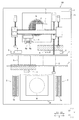
図1〜図4を参照して、本発明の一実施形態による部品実装装置100の構造について説明する。(Configuration of component mounting device)
The structure of the
部品実装装置100は、ダイシングされたウエハWから部品(半導体チップ)Cを取り出して基板Sの実装面上に実装するとともに、テープフィーダ3aにより供給される電子部品(いわゆるパッケージ部品)などを基板Sの実装面上に実装することが可能ないわゆる複合型の部品実装装置である。
The
この部品実装装置100は、図1に示すように、基台1と、コンベア2と、2つのチップ部品供給部3と、2つの実装部4と、ウエハ保持テーブル5と、取出部6と、部品認識カメラ7と、固定カメラ8と、フラックス供給部9と、ウエハ収納部10と、制御部11とを備えている。また、部品実装装置100は、図2に示すように、表示部12を備えている。また、部品実装装置100は、照明81を備えている。照明81は、メイン照明811と、同軸照明812と、サイド照明813とを含んでいる。なお、実装部4は、請求の範囲の「実装ヘッド」の一例であり、固定カメラ8は、請求の範囲の「撮像部」の一例である。
As shown in FIG. 1, the
コンベア2は、所定の実装作業位置に基板Sを搬入および搬出するように構成されている。また、コンベア2は、X方向に延びる一対のコンベアレールと、基板Sを所定位置で位置決めする位置決め機構(図示せず)とを含んでいる。これにより、コンベア2は、基板SをX方向に搬送し、所定の実装作業位置に基板Sを位置決め固定する。 The conveyor 2 is configured to carry in and out the substrate S to a predetermined mounting work position. Further, the conveyor 2 includes a pair of conveyor rails extending in the X direction and a positioning mechanism (not shown) for positioning the substrate S at a predetermined position. As a result, the conveyor 2 conveys the substrate S in the X direction, and positions and fixes the substrate S at a predetermined mounting work position.
2つのチップ部品供給部3は、それぞれ、部品実装装置100の手前側(Y1方向側)の両端に設けられている。チップ部品供給部3には、テープフィーダ3aがX方向に沿って並んで配置されている。各テープフィーダ3aは、キャリアテープを間欠的に送り出し、所定の部品供給位置にキャリアテープ内の電子部品を供給する。
The two chip component supply units 3 are provided at both ends on the front side (Y1 direction side) of the
実装部4は、チップ部品供給部3から供給される電子部品およびウエハWの部品Cを基板Sに実装するように構成されている。具体的には、実装部4は、XY移動機構により、コンベア2(基板S)の上方を水平方向(XY方向)に移動可能に支持されている。実装部4は、X方向に沿って配置された複数(2つ)の吸着ノズル4a(図3参照)を有している。部品Cは、たとえば、ウエハレベルパッケージ(WLP)や、ウエハレベルチップサイズパッケージ(WL−CSP)などである。
The mounting
また、実装部4は、取出部6によりウエハWから取り出される部品Cを吸着ノズル4aにより吸着して基板S上に実装するように構成されている。また、実装部4は、テープフィーダ3aによって供給される電子部品を吸着ノズル4aにより吸着して基板S上に実装するように構成されている。
Further, the mounting
ウエハ保持テーブル5は、出し入れ機構(図示せず)によりウエハ収納部10から引き出されたウエハWを所定位置で支持するように構成されている。
The wafer holding table 5 is configured to support the wafer W drawn out from the
取出部6は、ウエハWから部品Cを取り出して実装部4に受け渡すように構成されている。また、取出部6は、所定の駆動手段によりウエハ保持テーブル5の上方位置において水平方向(XY方向)に移動される。また、取出部6は、4つのウエハヘッド6a(図3参照)を含んでいる。
The take-out unit 6 is configured to take out the component C from the wafer W and deliver it to the mounting
ウエハヘッド6aは、X軸回りに回転が可能で、かつ上下方向への移動(昇降)が可能に構成されている。また、ウエハヘッド6aは、部品Cを吸着することが可能に構成されている。つまり、取出部6は、突上部(図示せず)により突き上げられた部品Cをウエハヘッド6aにより吸着して取り出し、部品Cを反転(フリップ)させ、所定の受け渡し位置において、実装部4(吸着ノズル4a)に部品Cを受け渡すように構成されている。
The
部品認識カメラ7は、ウエハWからの部品Cの取り出しに先立ち、取り出し対象となる部品Cを撮像するように構成されている。また、部品認識カメラ7は、取出部6と共通のフレームに設けられている。また、部品認識カメラ7は、所定の駆動手段によりウエハ保持テーブル5の上方位置において水平方向(XY方向)に移動される。部品認識カメラ7には、照明(図示せず)が設けられている。照明は、部品認識カメラ7による撮像の際に発光するように構成されている。照明は、LED(発光ダイオード)などの光源を有している。
The
固定カメラ8は、基台1上であって実装部4の可動領域内に設置されている。固定カメラ8は、実装部4の吸着ノズル4aにより吸着されている電子部品(部品Cを含む)を下側から撮像するように構成されている。固定カメラ8には、図2および図4に示すように、照明81が設けられている。照明81は、固定カメラ8による撮像の際に発光するように構成されている。照明81は、LED(発光ダイオード)などの光源を有している。
The fixed
図4に示すように、照明81は、メイン照明811と、同軸照明812と、サイド照明813とが撮像方法に応じて発光するように構成されている。メイン照明811は、上下方向(Z方向)に対して斜めに光を照射するように構成されている。具体的には、メイン照明811は、同軸照明812の外側を取り囲むように配置されている。また、メイン照明811は、斜め内側の上方に向けて光を照射するように構成されている。同軸照明812は、固定カメラ8の光軸と同軸方向に光を照射するように構成されている。つまり、同軸照明812は、上方向に向けて光を照射するように構成されている。サイド照明813は、部品Cに対して側方から光を照射するように構成されている。つまり、サイド照明813は、吸着ノズル4aに保持された部品Cに対して横から光を照射するように構成されている。
As shown in FIG. 4, the
照明81は、照射する光の強度を調整することが可能である。具体的には、照明81は、PWM制御(パルス幅変調制御)により、光の強度が調整される。また、照明81は、メイン照明811と、同軸照明812と、サイド照明813とを、個別に点灯させて光を照射することが可能に構成されている。また、照明81は、メイン照明811、同軸照明812、サイド照明813を組み合わせて光を照射することが可能に構成されている。たとえば、照明81は、メイン照明811および同軸照明812を組み合わせて光を照射するように構成されている。
The
フラックス供給部9は、部品Cのバンプ電極Bにフラックスを転写(塗布)するために設けられている。具体的には、フラックス供給部9は、プレート上にフラックスを薄く伸ばし広げて供給する。そして、実装部4の吸着ノズル4aに吸着された部品Cが伸び広げられたフラックスに接触される。これにより、部品Cのバンプ電極Bにフラックスが転写される。なお、フラックスは、接合のための半田の濡れが良好になるように部品Cのバンプ電極Bに塗布される。
The
ウエハ収納部10は、ダイシングされた複数枚のウエハWを収容可能に構成されている。ウエハWの部品Cは、たとえば、複数のバンプ電極Bが形成されたフリップチップ実装用のチップ部品である。つまり、部品Cの実装面には、実装面から突出した立体的な電極が複数設けられている。この場合、部品Cは、バンプ電極形成面(実装面)が上方を向くようにフィルム状のウエハシート上に貼り付けられて保持されている。
The
制御部11は、部品実装装置100の各部の動作を統括的に制御するように構成されている。具体的には、制御部11は、コンベア2、チップ部品供給部3、実装部4、ウエハ保持テーブル5、取出部6、部品認識カメラ7、固定カメラ8、フラックス供給部9およびウエハ収納部10などの動作制御を行うように構成されている。制御部11は、上記の各部の駆動モータに内蔵されるエンコーダ等の位置検出手段からの出力信号に基づいて、各部の動作制御を行う。また、制御部11は、各種カメラ(部品認識カメラ7および固定カメラ8)の撮像制御および画像認識を行う機能を有する。図2に示すように、制御部11は、CPU(中央処理ユニット)111と、メモリ112とを含んでいる。なお、メモリ112は、請求の範囲の「記憶部」の一例である。
The
表示部12には、情報が表示されるように構成されている。具体的には、表示部12には、部品実装装置100の操作のための情報が表示される。また、表示部12には、部品実装装置100の状態を示す情報が表示される。
The
(部品実装動作の説明)
次に、図3を参照して、部品実装装置100による電子部品の実装動作について説明する。(Explanation of component mounting operation)
Next, the mounting operation of the electronic component by the
図3に示すように、ウエハWの部品Cを基板Sに実装する場合、まず、取出部6により実装対象の部品Cが取り出されて、取出部6のウエハヘッド6aに部品Cが吸着保持される。ウエハヘッド6aが回動して部品Cが反転(フリップ)され、部品Cが所定の受け渡し位置に配置される。これに対応して、実装部4の吸着ノズル4aが受け渡し位置の上方で受け渡し高さ位置まで下降されて、部品Cが吸着される。
As shown in FIG. 3, when the component C of the wafer W is mounted on the substrate S, first, the component C to be mounted is taken out by the take-out unit 6, and the component C is attracted and held by the
部品Cが吸着された後、実装部4が、フラックス供給部9の上方に移動される。実装部4の吸着ノズル4aが転写高さ位置まで下降されて、部品Cのバンプ電極形成面にフラックスが転写(塗布)される。その後、実装部4が、固定カメラ8の上方を通過するように移動されて、吸着ノズル4aに吸着された部品Cのバンプ電極形成面が撮像される。これにより、部品Cのバンプ電極形成面の不良判定や、吸着位置ずれの認識が行われる。なお、この転写動作と撮像動作とは、順序が逆になる場合もある。すなわち、転写前の状態の方が良好に撮像(画像認識)を行える場合には、撮像動作が先に実施される。
After the component C is sucked, the mounting
撮像後、コンベア2に保持された基板Sの上方に実装部4が移動され、所定の実装位置の上方で吸着ノズル4aが実装高さ位置まで下降されて、部品Cが基板S上に載置(実装)される。
After imaging, the mounting
また、テープフィーダ3a(図1参照)の供給部品を実装する場合、実装部4がテープフィーダ3aの所定の部品取出位置の上方に移動される。そして、吸着ノズル4aが下降されて電子部品が取り出される。その後、実装部4が、固定カメラ8の上方を通過するように移動されて、吸着ノズル4aに吸着された電子部品の下面が撮像される。そして、実装部4が基板Sの上方に移動される。その後、吸着ノズル4aが下降されて、電子部品が基板S上に載置(実装)される。なお、部品Cがキャリアテープに個別収納されテープフィーダ3aから供給される場合には、テープフィーダ3aから部品Cが取り出された後、図3に示すように転写および撮像が実施され、基板S上に部品Cが載置(実装)される。
Further, when mounting the supply component of the
ここで、本実施形態では、制御部11は、固定カメラ8により撮像した部品Cの画像に基づいて、部品Cを認識するための部品データを作成する制御を行うように構成されている。また、制御部11は、部品Cを異なる撮影条件により撮像部により複数回撮像させて、部品データを作成する制御を行うように構成されている。
Here, in the present embodiment, the
具体的には、制御部11は、照明81による光の照射条件を異ならせて部品Cを固定カメラ8により複数回撮像させて、部品データを作成する制御を行うように構成されている。詳しくは、制御部11は、部品Cに対する光の照射方向を異ならせて部品Cを固定カメラ8により複数回撮像させて、部品データを作成する制御を行うように構成されている。
Specifically, the
制御部11は、部品Cに対して下方から光を照射して部品Cを撮像した画像と、部品Cに対して側方から光を照射して部品Cを撮像した画像とに基づいて、部品データを作成する制御を行うように構成されている。つまり、制御部11は、メイン照明811および同軸照明812を組み合わせて光を照射して、部品Cを撮像した画像と、サイド照明813から光を照射して部品Cを撮像した画像とに基づいて、部品データを作成するように構成されている。
The
また、制御部11は、第1撮像条件により撮像した部品Cの画像に基づいて、部品Cの外形を取得し、第1撮像条件とは異なる第2撮像条件により撮像した部品Cの画像に基づいて、部品Cの電極の配置情報を取得する制御を行うように構成されている。第1撮像条件では、部品Cに対して下方から光が照射されて撮像される。また、第2撮像条件では、部品Cに対して側方(サイド)から光が照射されて撮像される。
Further, the
また、制御部11は、第1撮像条件により部品Cを撮像した後、第2撮像条件により部品Cを撮像する制御を行うように構成されている。つまり、制御部11は、第1撮像条件により撮像した結果に基づいて、部品Cの外形を取得した後、第2撮像条件により撮像した結果に基づいて、部品Cの電極の配置情報を取得するように構成されている。
Further, the
制御部11は、照明81から部品Cに照射する光の量を異ならせて部品Cを固定カメラ8により複数回撮像させて、撮像した画像に基づいて、撮像時に適した光の量を取得する制御を行うように構成されている。たとえば、バンプ数、バンプ径が既知の場合や、容易に抽出できる場合、バンプの見やすい照度を自動で求める。複数の異なる照明レベルにより部品Cを撮像し、取得した画像に基づいて、バンプを抽出し、パンプ数やバンプ径などを求める。そして、既知の値に最も近い計測結果が得られた照明レベルを部品の適正照度として取得する。この照度を用いてバンプ座標データ作成、実生産時の部品認識を行う。
The
制御部11は、複数の立体的な電極を含む部品Cの外形寸法、電極の配置情報、電極の寸法を、部品Cを撮像した画像に基づいて取得する制御を行うように構成されている。また、制御部11は、部品Cを撮像した画像の抽出箇所の特徴量を利用して、部品Cの電極とノイズとを判別する制御を行うように構成されている。
The
具体的には、図5に示すように、グレイスケール解析を行う場合は、撮像画像に基づいて、画像の部分を膨張・収縮処理を行う。また、バイナリ解析を行う場合は、撮像画像に基づいて、二値化処理を行った上で、画像の部分を膨張・収縮処理を行う。これにより、微小ノイズ成分を除去することが可能である。その後、輪郭追跡を行い、特徴量を算出する。特徴量は、たとえば、面積、面積を同等面積円とした直径換算値、周囲長、周囲長を同等円周囲長とした直径換算値、包含円直径(外接円の直径)、長径・短径、真円度(最大半径と最少半径との差)、円形度、水平ー垂直フィレ径、算術的なモーメントなどを含む。特徴量を算出した結果を用いて、バンプ電極Bの形状は円形であるとして、形状の歪みやサイズによりノイズを自動的に除去することが可能である。たとえば、円に対して大きく歪んでいる場合にノイズとして除去する。この場合、オペレータに除去すべきか確認することもできる。また、ボール径が未知の場合でも、歪み量を用いればノイズを除去することが可能である。事前にバンプ電極Bの径(ボール径)を取得している場合、計測方法・特徴量算出結果からノイズを自動判定し除去する。これにより、不要箇所の過剰抽出を抑制することが可能である。 Specifically, as shown in FIG. 5, when performing grayscale analysis, a portion of the image is expanded / contracted based on the captured image. In addition, when performing binary analysis, after performing binarization processing based on the captured image, the image portion is expanded / contracted. This makes it possible to remove minute noise components. After that, contour tracking is performed and the feature amount is calculated. The feature quantities are, for example, diameter conversion value with area and area as equivalent area circle, peripheral length, diameter conversion value with peripheral length as equivalent circle peripheral length, included circle diameter (diameter of circumscribing circle), major axis / minor axis, Includes roundness (difference between maximum and minimum radius), circularity, horizontal-vertical fillet diameter, mathematical moments, etc. Using the result of calculating the feature amount, assuming that the shape of the bump electrode B is circular, it is possible to automatically remove noise due to the distortion and size of the shape. For example, if it is greatly distorted with respect to a circle, it is removed as noise. In this case, the operator can also ask if it should be removed. Further, even when the ball diameter is unknown, it is possible to remove noise by using the amount of strain. When the diameter (ball diameter) of the bump electrode B is acquired in advance, noise is automatically determined and removed from the measurement method / feature amount calculation result. This makes it possible to suppress excessive extraction of unnecessary parts.
制御部11は、部品Cを撮像した画像に基づいて複数の電極を含む部品Cの電極の配置情報を取得する制御を行うように構成されている。そして、部品実装装置100は、複数の電極のうち、配置情報を取得する必要のない部分が設定可能に構成されている。具体的には、図6に示すように、バンプ情報取得不要部分を事前に設定して画像解析から除外される。たとえば、オペレータがマウス操作によりバンプ情報取得不要部分を選択して、除外する。バンプ情報取得不要部分は、部品Cの良否判定に不要な部分である。図6の例では、左上の複数のバンプグループの情報が不要として除外されている。
The
制御部11は、部品Cを撮像した画像に基づいて、部品Cの電極の判別が困難な場合に、判別困難な部分を表示部12に表示する制御を行うように構成されている。具体的には、図7に示す例のように、電極の判別ができたバンプ電極Bには、ガイド201aが付される。また、電極の判別が困難な部分には、ガイド201bが付される。たとえば、バンプ径が事前にわからない場合などに、形状に歪みが見られた箇所を部品画像上に計測情報をオーバーレイしてガイド201bを付してオペレータに示す。ガイド201aおよび201bは、オペレータに識別可能に表示される。たとえば、ガイド201aおよび201bは、互いに異なる色、形状、表示方法(点滅表示等)などにより表示される。バンプ径や歪みは、複数の抽出箇所の統計に基づく分布により判定される。オペレータは、ガイド201bが付されて示された箇所を個別にバンプ/ノイズを判定して処理を行う。
The
また、図8に示すように、バンプ径の自動算出が困難である場合に、設定候補の状態を部品画像上にオーバーレイしてサイズ表示202a、202bまたは202cを付してオペレータに示す。オペレータは、サイズ表示202a〜202cと、画像上の抽出部分とを比較して、バンプ径を選択して決定する。また、設計値の径と画像上の径とが一致しない場合、画像上の径に合わせて部品データが作成される。つまり、部品Cを実装する際に、実際に撮像される画像に合うように部品データが作成される。
Further, as shown in FIG. 8, when it is difficult to automatically calculate the bump diameter, the state of the setting candidate is overlaid on the component image and the
図9に示すように、照明条件を変えることにより、部品Cの映されやすい部分と映されにくい部分とが異なる。図9の(A)のメイン照明811により撮像した場合、(B)の同軸照明812により撮像した場合、(C)のメイン照明811および同軸照明812により撮像した場合は、部品C上のマークが映りこむ。一方(D)のサイド照明813により撮像した場合は、部品C上のマークが映りこまない。つまり、見たい箇所、見たくない箇所が区別しやすい照明条件に切り替え、部品画像を複数枚取得する。具体的には、部品外形から搭載基準/バンプ配置基準となる部品Cの中心位置を取得した場合、外形部分が最も見えるメイン照明811および同軸照明812を用いて撮像する。また、バンプの位置を取得したい場合、外形やマークやパターンなどの映りこみが無くバンプが見えるサイド照明813を用いて撮像する。つまり、バンプは、部品Cの実装面に対して突出して配置されているため、サイドから光を当てた場合でも、鮮明に撮像することが可能である。
As shown in FIG. 9, by changing the lighting conditions, the portion of the component C that is easily projected and the portion that is not easily projected are different. When the image is taken with the
複数のバンプは、グループに分けて認識される。たとえば、全て必要な電極であるグループ、接地用電極などで、所定数以上あればよいグループ、結合補強用電極などで、特に必要ないグループなどに分けられる。制御部11は、グループ毎に認識数、欠落数の閾値を変えて、バンプを認識して部品データを作成する。
Multiple bumps are recognized as groups. For example, it is divided into a group in which all necessary electrodes are required, a group in which a predetermined number or more of electrodes for grounding are required, and a group in which electrodes for coupling reinforcement are not particularly necessary. The
作成された部品データは、メモリ112に格納される。制御部11は、作成した部品データと、メモリ112に記憶された部品データとを比較し、書き換え可能である場合に、作成した部品データに書き換えるように構成されている。つまり、部品データがメモリ112に重複して記憶されるのが抑制される。
The created component data is stored in the
(部品データ作成処理)
図10を参照して、部品実装装置100の制御部11による部品データ作成処理についてフローチャートに基づいて説明する。(Part data creation process)
With reference to FIG. 10, the component data creation process by the
図10のステップS1において、固定カメラ8による1回目の撮像が行われる。具体的には、吸着ノズル4aにより吸着された部品Cが固定カメラ8の上方に位置されて、部品Cの撮像が行われる。ステップS2において、吸着ずれ角度、部品の外形寸法、部品中心位置が算出される。
In step S1 of FIG. 10, the first imaging by the fixed
ステップS3において、算出結果が表示部12に表示される。表示部12の表示に基づいて、必要に応じてオペレータが結果の微調整を行う。ステップS4において、ずれ角度分だけ、部品Cが回動される。具体的には、角度がずれている分だけ、反対方向に吸着ノズル4aが回動される。
In step S3, the calculation result is displayed on the
ステップS5において、固定カメラ8による2回目の撮像が行われる。この際、1回目の撮像とは異なる撮像条件により部品Cが撮像される。ステップS6において、撮像した画像からバンプが抽出される。具体的には、画像からバンプ位置およびバンプ径が抽出される。
In step S5, the second imaging by the fixed
ステップS7において、抽出したバンプが表示部12に表示される。表示部12の表示に基づいて、必要に応じてオペレータが結果の微調整を行う。具体的には、オペレータにより生産時チェック不要バンプ、誤作成バンプ、ノイズ判断不可能な箇所の削除操作が行われる。また、オペレータにより適正なバンプの径選択操作が行われる。ステップS8において、バンプ径の変更が有るか否かが判断される。変更が有れば、ステップS9に進み、変更が無ければ、ステップS10に進む。
In step S7, the extracted bumps are displayed on the
ステップS9において、バンプが再度抽出される。また、選択されたバンプ径によりバンプ径データが再度作成される。その後、ステップS10に進む。ステップS10において、既存類似データが確認される。つまり、作成された部品データと類似のデータがデータベース上に無いかをチェックする。 In step S9, the bumps are extracted again. Also, the bump diameter data is recreated with the selected bump diameter. After that, the process proceeds to step S10. In step S10, existing similar data is confirmed. That is, it checks whether there is any data similar to the created part data in the database.
ステップS11において、類似データが有るか否かが判断される。類似データが有れば、ステップS12に進み、類似データが無ければ、ステップS14に進む。ステップS12において、データ置換指示が有るか否かが判断される。つまり、オペレータにより類似データに対して新しいデータを置換して保存するという指示が有るか否かが判断される。置換指示が有れば、ステップS13によりデータを置換してステップS14に進む。置換指示が無ければ、ステップS14に進む In step S11, it is determined whether or not there is similar data. If there is similar data, the process proceeds to step S12, and if there is no similar data, the process proceeds to step S14. In step S12, it is determined whether or not there is a data replacement instruction. That is, it is determined whether or not the operator gives an instruction to replace and save new data for similar data. If there is a replacement instruction, the data is replaced in step S13 and the process proceeds to step S14. If there is no replacement instruction, the process proceeds to step S14.
ステップS14において、バンプのグループ設定を受け付ける。その後、部品データ作成処理が終了される。 In step S14, the bump group setting is accepted. After that, the component data creation process is completed.
(実施形態の効果)
本実施形態では、以下のような効果を得ることができる。(Effect of embodiment)
In this embodiment, the following effects can be obtained.
本実施形態では、上記のように、制御部11を、部品Cを異なる撮影条件により固定カメラ8により複数回撮像させて、部品データを作成する制御を行うように構成する。これにより、1回の撮像により部品Cの全ての特徴点が画像に鮮明に映らない場合でも、複数の撮像条件により撮像することにより、部品Cの特徴点を複数の画像のいずれかにより鮮明に撮像することができる。これにより、自動で取得することが可能な特徴点の情報数を多くすることができるので、オペレータにより入力する特徴点の情報数を減少させることができる。これにより、誤入力の発生を抑制することができる。その結果、オペレータの作業負担を軽減するとともに、精度よく部品データを作成することができる。
In the present embodiment, as described above, the
また、本実施形態では、上記のように、制御部11を、照明81による光の照射条件を異ならせて部品Cを固定カメラ8により複数回撮像させて、部品データを作成する制御を行うように構成する。これにより、光の照射条件により見え方が変化する部品Cを、複数の光の照射条件により撮像することができるので、部品Cの特徴点を認識することができる数を効果的に多くすることができる。
Further, in the present embodiment, as described above, the
また、本実施形態では、上記のように、制御部11を、部品Cに対する光の照射方向を異ならせて部品Cを固定カメラ8により複数回撮像させて、部品データを作成する制御を行うように構成する。これにより、光の照射方向により光の反射方向が変化する特徴点を有する部品Cを、光の照射方向を変えた複数の照射条件により撮像することができるので、部品Cの特徴点を認識することができる数をより効果的に多くすることができる。
Further, in the present embodiment, as described above, the
また、本実施形態では、上記のように、制御部11を、照明81から部品Cに照射する光の量を異ならせて部品Cを固定カメラ8により複数回撮像させて、撮像した画像に基づいて、撮像時に適した光の量を取得する制御を行うように構成する。これにより、部品Cを認識するために撮影する際の光の量を最適化することができるので、基板Sへの部品実装時における部品Cの認識精度を向上させることができる。
Further, in the present embodiment, as described above, the
また、本実施形態では、上記のように、制御部11を、部品Cに対して下方から光を照射して部品Cを撮像した画像と、部品Cに対して側方から光を照射して部品Cを撮像した画像とに基づいて、部品データを作成する制御を行うように構成する。これにより、部品Cに下方から光を照射して撮像した画像に基づいて、部品Cの外形を容易に認識することができるとともに、部品Cに側方から光を照射した画像に基づいて、下方に突出する複数のバンプ電極Bの位置を容易に認識することができる。
Further, in the present embodiment, as described above, the
また、本実施形態では、上記のように、制御部11を、第1撮像条件により撮像した部品Cの画像に基づいて、部品Cの外形を取得し、第1撮像条件とは異なる第2撮像条件により撮像した部品Cの画像に基づいて、部品Cの電極の配置情報を取得する制御を行うように構成する。これにより、部品Cの外形が鮮明に映りやすい第1撮像条件により撮像した画像と、部品Cの電極が鮮明に映りやすい第2撮像条件により撮像した画像とにより、部品データを容易に精度よく作成することができる。
Further, in the present embodiment, as described above, the
また、本実施形態では、上記のように、制御部11を、第1撮像条件により部品Cを撮像した後、第2撮像条件により部品Cを撮像する制御を行うように構成する。これにより、部品Cの外形を取得した後、部品Cの外形に基づく基準位置に対して電極の位置を関連付けて取得することができるので、効率よく部品データを作成することができる。
Further, in the present embodiment, as described above, the
また、本実施形態では、上記のように、制御部11を、複数の立体的な電極を含む部品Cの外形寸法、電極の配置情報、電極の寸法を、部品Cを撮像した画像に基づいて取得する制御を行うように構成する。これにより、部品Cを実装する際の固定カメラ8の撮像結果に基づいて、部品データを取得することができるので、部品Cの外形寸法、電極の寸法、電極の配置の計測ミスを抑制することができる。これにより、部品Cの実装時に良品の部品Cを誤って不良品と判定して廃棄するのを抑制することができる。また、ノギスなどの計測器具を用いてオペレータが手動で測定する必要がないので、部品データ作成時間が増加するのを抑制することができる。
Further, in the present embodiment, as described above, the
また、本実施形態では、上記のように、制御部11を、部品Cを撮像した画像の抽出箇所の特徴量を利用して、部品Cの電極とノイズとを判別する制御を行うように構成する。これにより、部品データにノイズが混入するのを抑制することができる。また、ノイズの混入を抑制することができるので、オペレータが確認する必要がある場合でも、確認作業を短時間で行うことができる。
Further, in the present embodiment, as described above, the
また、本実施形態では、上記のように、制御部11を、部品Cを撮像した画像に基づいて複数の電極を含む部品Cの電極の配置情報を取得する制御を行うように構成され、複数の電極のうち、配置情報を取得する必要のない部分が設定可能に構成する。これにより、必要のない部分の電極の配置情報を取得することを省略することができるので、より短時間で部品データを作成することができる。
Further, in the present embodiment, as described above, the
また、本実施形態では、上記のように、制御部11を、部品Cを撮像した画像に基づいて、部品Cの電極の判別が困難な場合に、判別困難な部分を表示部12に表示する制御を行うように構成する。これにより、オペレータにより、判別困難な部分の情報を入力することができるので、精度よく部品データを作成することができる。
Further, in the present embodiment, as described above, when it is difficult to discriminate the electrodes of the component C based on the image obtained by capturing the image of the component C, the
また、本実施形態では、上記のように、制御部11を、作成した部品データと、メモリ112に記憶された部品データとを比較し、書き換え可能である場合に、作成した部品データに書き換えるように構成する。これにより、部品データの重複を抑制することができるので、データ管理を容易に行うことができる。
Further, in the present embodiment, as described above, the
(変形例)
なお、今回開示された実施形態は、すべての点で例示であって制限的なものではないと考えられるべきである。本発明の範囲は、上記した実施形態の説明ではなく請求の範囲によって示され、さらに請求の範囲と均等の意味および範囲内でのすべての変更(変形例)が含まれる。(Modification example)
It should be noted that the embodiments disclosed this time are exemplary in all respects and are not considered to be restrictive. The scope of the present invention is shown by the claims rather than the description of the above-described embodiment, and further includes all modifications (modifications) within the meaning and scope equivalent to the claims.
たとえば、上記実施形態では、チップ部品を基板に実装する部品実装装置に本発明を適用する構成の例を示したが、本発明はこれに限られない。本発明では、テープやトレイにより供給される部品を基板に実装する部品実装装置に本発明を適用してもよい。たとえば、リード部品を撮像して、部品データとして、リード部品の部品データを作成してもよい。 For example, in the above embodiment, an example of a configuration in which the present invention is applied to a component mounting device for mounting a chip component on a substrate is shown, but the present invention is not limited to this. In the present invention, the present invention may be applied to a component mounting device for mounting components supplied by a tape or a tray on a substrate. For example, the lead component may be imaged and the component data of the lead component may be created as the component data.
また、上記実施形態では、部品データを作成する際に、異なる2つの撮像条件により部品を撮像する構成の例を示したが、本発明はこれに限られない。本発明では、異なる3以上の撮像条件により部品を撮像して各々撮像結果に基づいて部品データを作成してもよい。 Further, in the above embodiment, an example of a configuration in which a component is imaged under two different imaging conditions when creating component data is shown, but the present invention is not limited to this. In the present invention, parts may be imaged under three or more different imaging conditions, and component data may be created based on the imaging results.
また、上記実施形態では、部品データを作成する際に、光らせる照明を異ならせて撮像条件を互いに異ならせて部品の撮像を行う構成の例を示したが、本発明はこれに限られない。本発明では、撮像する位置や撮像する方向などの条件を異ならせて部品の撮像を行ってもよい。 Further, in the above-described embodiment, when creating component data, an example of a configuration in which components are imaged by different lightings to be illuminated and different imaging conditions from each other is shown, but the present invention is not limited to this. In the present invention, the components may be imaged under different conditions such as the position to be imaged and the direction to be imaged.
また、上記実施形態では、部品を撮像した画像に基づいて、部品データを作成する構成の例を示したが、本発明はこれに限られない。本発明では、部品を撮像した画像に加えて、既知のデータを用いて、部品データを作成してもよい。 Further, in the above embodiment, an example of a configuration in which component data is created based on an image obtained by capturing an image of a component is shown, but the present invention is not limited to this. In the present invention, the component data may be created by using the known data in addition to the image obtained by capturing the component.
また、上記実施形態では、説明の便宜上、制御部の処理を処理フローに沿って順番に処理を行うフロー駆動型のフローを用いて説明したが、本発明はこれに限られない。本発明では、制御部の処理を、イベント単位で処理を実行するイベント駆動型(イベントドリブン型)の処理により行ってもよい。この場合、完全なイベント駆動型で行ってもよいし、イベント駆動およびフロー駆動を組み合わせて行ってもよい。 Further, in the above-described embodiment, for convenience of explanation, the processing of the control unit has been described using a flow-driven flow in which the processing is sequentially performed along the processing flow, but the present invention is not limited to this. In the present invention, the processing of the control unit may be performed by an event-driven type (event-driven type) processing in which the processing is executed in event units. In this case, it may be completely event-driven, or it may be a combination of event-driven and flow-driven.
4 実装部(実装ヘッド)
8 固定カメラ(撮像部)
11 制御部
12 表示部
81 照明
112 メモリ(記憶部)
B バンプ電極
C 部品
S 基板4 Mounting part (mounting head)
8 Fixed camera (imaging unit)
11
B Bump electrode C component S substrate
Claims (13)
部品を撮像可能な撮像部と、
前記撮像部により撮像した部品の画像に基づいて、部品を認識するための部品データを作成する制御部とを備え、
前記制御部は、部品を異なる撮影条件により前記撮像部により複数回撮像させて、前記部品データを作成する制御を行うとともに、前記部品データを作成する際に、部品に対して下方から光を照射して部品を撮像した画像に基づいて、部品の外形を取得し、部品に対して側方から光を照射して部品を撮像した画像に基づいて、部品の電極の位置および大きさを取得するように構成されている、部品実装装置。 A mounting head that mounts components on the board,
An imaging unit that can image parts and
A control unit that creates component data for recognizing a component based on an image of the component captured by the imaging unit is provided.
The control unit controls to create the component data by imaging the component a plurality of times by the imaging unit under different shooting conditions , and irradiates the component with light from below when creating the component data. The outer shape of the component is acquired based on the image of the component, and the position and size of the electrode of the component are acquired based on the image of the component by irradiating the component with light from the side. A component mounting device that is configured as such.
前記制御部は、前記照明による光の照射条件を異ならせて部品を前記撮像部により複数回撮像させて、前記部品データを作成する制御を行うように構成されている、請求項1に記載の部品実装装置。 It is equipped with an illumination that irradiates the component with light during imaging by the imaging unit.
The first aspect of the present invention, wherein the control unit controls to create the component data by capturing images of the component a plurality of times by the imaging unit with different irradiation conditions of light by the illumination. Component mounting device.
前記制御部は、部品に対して下方から光を照射して部品を撮像した画像と、部品に対して側方から光を照射して部品を撮像した画像とに基づいて、前記部品データを作成する制御を行うように構成されている、請求項2〜4のいずれか1項に記載の部品実装装置。 The component contains multiple bump electrodes
The control unit creates the component data based on an image in which the component is imaged by irradiating the component with light from below and an image in which the component is imaged by irradiating the component with light from the side. The component mounting apparatus according to any one of claims 2 to 4, which is configured to perform control.
複数の電極のうち、配置情報を取得する必要のない部分が設定可能に構成されている、請求項1〜9のいずれか1項に記載の部品実装装置。 The control unit is configured to control acquisition of electrode arrangement information of a component including a plurality of electrodes based on an image obtained by capturing an image of the component.
The component mounting device according to any one of claims 1 to 9, wherein a portion of the plurality of electrodes that does not need to acquire arrangement information is configured to be configurable.
前記制御部は、部品を撮像した画像に基づいて、部品の電極の判別が困難な場合に、判別困難な部分を前記表示部に表示する制御を行うように構成されている、請求項1〜10のいずれか1項に記載の部品実装装置。 Equipped with a display unit that displays information
The control unit is configured to control the display unit to display the difficult-to-discriminate portion when it is difficult to discriminate the electrodes of the component based on an image obtained by capturing an image of the component. The component mounting device according to any one of 10.
前記制御部は、作成した前記部品データと、前記記憶部に記憶された前記部品データとを比較し、書き換え可能である場合に、作成した前記部品データに書き換えるように構成されている、請求項1〜11のいずれか1項に記載の部品実装装置。 A storage unit for storing the component data is provided.
The control unit is configured to compare the created component data with the component data stored in the storage unit and, if rewritable, rewrite the created component data. The component mounting device according to any one of 1 to 11.
前記撮像部により撮像した部品の画像に基づいて、部品を認識するための部品データを作成し、
前記部品データを作成することは、部品に対して下方から光を照射して部品を撮像した画像に基づいて、部品の外形を取得し、部品に対して側方から光を照射して部品を撮像した画像に基づいて、部品の電極の位置および大きさを取得することを含む、部品データ作成方法。 The parts are imaged multiple times by the imaging unit under different imaging conditions.
Based on the part of the image captured by the imaging unit, to create the part data for recognizing the part products,
To create the component data, the external shape of the component is acquired based on the image obtained by irradiating the component with light from below and the component is imaged, and the component is irradiated with light from the side. A method of creating component data , including acquiring the position and size of electrode of a component based on an captured image .
Applications Claiming Priority (1)
| Application Number | Priority Date | Filing Date | Title |
|---|---|---|---|
| PCT/JP2017/023376 WO2019003267A1 (en) | 2017-06-26 | 2017-06-26 | Component mounting device and component data creation method |
Publications (2)
| Publication Number | Publication Date |
|---|---|
| JPWO2019003267A1 JPWO2019003267A1 (en) | 2019-11-21 |
| JP6831460B2 true JP6831460B2 (en) | 2021-02-17 |
Family
ID=64742839
Family Applications (1)
| Application Number | Title | Priority Date | Filing Date |
|---|---|---|---|
| JP2019526402A Active JP6831460B2 (en) | 2017-06-26 | 2017-06-26 | Component mounting device and component data creation method |
Country Status (2)
| Country | Link |
|---|---|
| JP (1) | JP6831460B2 (en) |
| WO (1) | WO2019003267A1 (en) |
Family Cites Families (12)
| Publication number | Priority date | Publication date | Assignee | Title |
|---|---|---|---|---|
| JPH05296725A (en) * | 1992-04-24 | 1993-11-09 | Matsushita Electric Ind Co Ltd | Position detecting method |
| JPH0738294A (en) * | 1993-07-26 | 1995-02-07 | Matsushita Electric Ind Co Ltd | Electronic component packaging device |
| JP2001135999A (en) * | 1999-11-09 | 2001-05-18 | Matsushita Electric Ind Co Ltd | Method for creating part library and device thereof |
| JP4387572B2 (en) * | 2000-09-27 | 2009-12-16 | ヤマハ発動機株式会社 | Component recognition control method and component recognition control device |
| JP3866688B2 (en) * | 2003-06-13 | 2007-01-10 | 三井金属鉱業株式会社 | Inspection device for film carrier tape for mounting electronic components and method for checking pattern defects |
| JP4381764B2 (en) * | 2003-09-29 | 2009-12-09 | ヤマハ発動機株式会社 | IMAGING DEVICE AND OBJECT MOVING DEVICE EQUIPPED WITH THE DEVICE |
| JP4324442B2 (en) * | 2003-10-16 | 2009-09-02 | Juki株式会社 | Component data generation device and electronic component mounting device |
| JP4913720B2 (en) * | 2007-12-28 | 2012-04-11 | 株式会社日立ハイテクインスツルメンツ | Electronic component mounting method for electronic component mounting apparatus |
| JP5926881B2 (en) * | 2010-03-30 | 2016-05-25 | 富士機械製造株式会社 | Image processing component data creation method and image processing component data creation device |
| JP2013191775A (en) * | 2012-03-14 | 2013-09-26 | Panasonic Corp | Component mounting device and component shape measuring method |
| EP2903406B1 (en) * | 2012-09-28 | 2023-10-25 | FUJI Corporation | System for correcting image processing data, and method for correcting image processing data |
| JP6147927B2 (en) * | 2014-05-30 | 2017-06-14 | ヤマハ発動機株式会社 | Component data generation apparatus, surface mounter, and component data generation method |
-
2017
- 2017-06-26 JP JP2019526402A patent/JP6831460B2/en active Active
- 2017-06-26 WO PCT/JP2017/023376 patent/WO2019003267A1/en active Application Filing
Also Published As
| Publication number | Publication date |
|---|---|
| JPWO2019003267A1 (en) | 2019-11-21 |
| WO2019003267A1 (en) | 2019-01-03 |
Similar Documents
| Publication | Publication Date | Title |
|---|---|---|
| JP5780712B2 (en) | Imaging system and electronic circuit component mounting machine | |
| CN108573901B (en) | Bare chip bonding apparatus and method for manufacturing semiconductor device | |
| WO2007033349A1 (en) | Pick and place machine with improved component pick image processing | |
| JP6378053B2 (en) | Component mounting machine and component mounting head | |
| US20220199433A1 (en) | Die Bonding Apparatus and Manufacturing Method for Semiconductor Apparatus | |
| JP6785407B2 (en) | Bump electronic component mounting device and bump electronic component mounting method | |
| JP6762527B2 (en) | Component mounting machine and component mounting head | |
| JP6714729B2 (en) | Surface mounter, component recognition device, component recognition method | |
| JP6831460B2 (en) | Component mounting device and component data creation method | |
| WO2018158888A1 (en) | Backup-pin recognizing method and component mounting device | |
| JP6612845B2 (en) | Mounting apparatus, imaging processing method, and imaging unit | |
| JP5040829B2 (en) | Component mounting apparatus and component mounting method | |
| EP3634100B1 (en) | Work machine, and calculation method | |
| JP5443894B2 (en) | Electronic component mounting apparatus and suction position correction method thereof | |
| JP6482165B2 (en) | Recognition device and recognition method | |
| JP2005175307A (en) | Method and device for recognizing part, surface mounting machine, part testing device and substrate inspection device | |
| CN112262621A (en) | Working machine | |
| JP2003304095A (en) | Electronic circuit component holding power acquiring program of suction nozzle and electronic circuit component handler | |
| JP7050926B2 (en) | Foreign matter detection method and electronic component mounting device | |
| JP2001217599A (en) | Surface mounting component attaching device and electronic component detecting method thereof | |
| JP2005093906A (en) | Component recognition device, surface mounting apparatus mounting the same, and component test device | |
| JPH07193398A (en) | Automatic assembly/mounting device and its method | |
| JP2018037591A (en) | Mounting device | |
| JP2021072019A (en) | Component mounting device, and component recognition method | |
| JP2012059735A (en) | Component mounting method and component mounting apparatus |
Legal Events
| Date | Code | Title | Description |
|---|---|---|---|
| A521 | Request for written amendment filed |
Free format text: JAPANESE INTERMEDIATE CODE: A523 Effective date: 20190806 |
|
| A621 | Written request for application examination |
Free format text: JAPANESE INTERMEDIATE CODE: A621 Effective date: 20190806 |
|
| A131 | Notification of reasons for refusal |
Free format text: JAPANESE INTERMEDIATE CODE: A131 Effective date: 20200804 |
|
| A521 | Request for written amendment filed |
Free format text: JAPANESE INTERMEDIATE CODE: A523 Effective date: 20200907 |
|
| TRDD | Decision of grant or rejection written | ||
| A01 | Written decision to grant a patent or to grant a registration (utility model) |
Free format text: JAPANESE INTERMEDIATE CODE: A01 Effective date: 20210126 |
|
| A61 | First payment of annual fees (during grant procedure) |
Free format text: JAPANESE INTERMEDIATE CODE: A61 Effective date: 20210128 |
|
| R150 | Certificate of patent or registration of utility model |
Ref document number: 6831460 Country of ref document: JP Free format text: JAPANESE INTERMEDIATE CODE: R150 |
|
| R250 | Receipt of annual fees |
Free format text: JAPANESE INTERMEDIATE CODE: R250 |