JP6820909B2 - Vehicle lighting fixtures and their lighting circuits - Google Patents
Vehicle lighting fixtures and their lighting circuits Download PDFInfo
- Publication number
- JP6820909B2 JP6820909B2 JP2018503083A JP2018503083A JP6820909B2 JP 6820909 B2 JP6820909 B2 JP 6820909B2 JP 2018503083 A JP2018503083 A JP 2018503083A JP 2018503083 A JP2018503083 A JP 2018503083A JP 6820909 B2 JP6820909 B2 JP 6820909B2
- Authority
- JP
- Japan
- Prior art keywords
- signal
- frequency
- circuit
- switching
- voltage
- Prior art date
- Legal status (The legal status is an assumption and is not a legal conclusion. Google has not performed a legal analysis and makes no representation as to the accuracy of the status listed.)
- Active
Links
Images


Classifications
-
- H—ELECTRICITY
- H05—ELECTRIC TECHNIQUES NOT OTHERWISE PROVIDED FOR
- H05B—ELECTRIC HEATING; ELECTRIC LIGHT SOURCES NOT OTHERWISE PROVIDED FOR; CIRCUIT ARRANGEMENTS FOR ELECTRIC LIGHT SOURCES, IN GENERAL
- H05B45/00—Circuit arrangements for operating light-emitting diodes [LED]
- H05B45/30—Driver circuits
- H05B45/37—Converter circuits
- H05B45/3725—Switched mode power supply [SMPS]
-
- B—PERFORMING OPERATIONS; TRANSPORTING
- B60—VEHICLES IN GENERAL
- B60Q—ARRANGEMENT OF SIGNALLING OR LIGHTING DEVICES, THE MOUNTING OR SUPPORTING THEREOF OR CIRCUITS THEREFOR, FOR VEHICLES IN GENERAL
- B60Q1/00—Arrangement of optical signalling or lighting devices, the mounting or supporting thereof or circuits therefor
- B60Q1/02—Arrangement of optical signalling or lighting devices, the mounting or supporting thereof or circuits therefor the devices being primarily intended to illuminate the way ahead or to illuminate other areas of way or environments
- B60Q1/04—Arrangement of optical signalling or lighting devices, the mounting or supporting thereof or circuits therefor the devices being primarily intended to illuminate the way ahead or to illuminate other areas of way or environments the devices being headlights
- B60Q1/14—Arrangement of optical signalling or lighting devices, the mounting or supporting thereof or circuits therefor the devices being primarily intended to illuminate the way ahead or to illuminate other areas of way or environments the devices being headlights having dimming means
- B60Q1/1415—Dimming circuits
-
- H—ELECTRICITY
- H01—ELECTRIC ELEMENTS
- H01L—SEMICONDUCTOR DEVICES NOT COVERED BY CLASS H10
- H01L33/00—Semiconductor devices with at least one potential-jump barrier or surface barrier specially adapted for light emission; Processes or apparatus specially adapted for the manufacture or treatment thereof or of parts thereof; Details thereof
-
- H—ELECTRICITY
- H02—GENERATION; CONVERSION OR DISTRIBUTION OF ELECTRIC POWER
- H02M—APPARATUS FOR CONVERSION BETWEEN AC AND AC, BETWEEN AC AND DC, OR BETWEEN DC AND DC, AND FOR USE WITH MAINS OR SIMILAR POWER SUPPLY SYSTEMS; CONVERSION OF DC OR AC INPUT POWER INTO SURGE OUTPUT POWER; CONTROL OR REGULATION THEREOF
- H02M1/00—Details of apparatus for conversion
- H02M1/08—Circuits specially adapted for the generation of control voltages for semiconductor devices incorporated in static converters
-
- H—ELECTRICITY
- H02—GENERATION; CONVERSION OR DISTRIBUTION OF ELECTRIC POWER
- H02M—APPARATUS FOR CONVERSION BETWEEN AC AND AC, BETWEEN AC AND DC, OR BETWEEN DC AND DC, AND FOR USE WITH MAINS OR SIMILAR POWER SUPPLY SYSTEMS; CONVERSION OF DC OR AC INPUT POWER INTO SURGE OUTPUT POWER; CONTROL OR REGULATION THEREOF
- H02M1/00—Details of apparatus for conversion
- H02M1/44—Circuits or arrangements for compensating for electromagnetic interference in converters or inverters
-
- H—ELECTRICITY
- H02—GENERATION; CONVERSION OR DISTRIBUTION OF ELECTRIC POWER
- H02M—APPARATUS FOR CONVERSION BETWEEN AC AND AC, BETWEEN AC AND DC, OR BETWEEN DC AND DC, AND FOR USE WITH MAINS OR SIMILAR POWER SUPPLY SYSTEMS; CONVERSION OF DC OR AC INPUT POWER INTO SURGE OUTPUT POWER; CONTROL OR REGULATION THEREOF
- H02M3/00—Conversion of dc power input into dc power output
- H02M3/02—Conversion of dc power input into dc power output without intermediate conversion into ac
- H02M3/04—Conversion of dc power input into dc power output without intermediate conversion into ac by static converters
- H02M3/10—Conversion of dc power input into dc power output without intermediate conversion into ac by static converters using discharge tubes with control electrode or semiconductor devices with control electrode
- H02M3/145—Conversion of dc power input into dc power output without intermediate conversion into ac by static converters using discharge tubes with control electrode or semiconductor devices with control electrode using devices of a triode or transistor type requiring continuous application of a control signal
- H02M3/155—Conversion of dc power input into dc power output without intermediate conversion into ac by static converters using discharge tubes with control electrode or semiconductor devices with control electrode using devices of a triode or transistor type requiring continuous application of a control signal using semiconductor devices only
- H02M3/156—Conversion of dc power input into dc power output without intermediate conversion into ac by static converters using discharge tubes with control electrode or semiconductor devices with control electrode using devices of a triode or transistor type requiring continuous application of a control signal using semiconductor devices only with automatic control of output voltage or current, e.g. switching regulators
-
- H—ELECTRICITY
- H05—ELECTRIC TECHNIQUES NOT OTHERWISE PROVIDED FOR
- H05B—ELECTRIC HEATING; ELECTRIC LIGHT SOURCES NOT OTHERWISE PROVIDED FOR; CIRCUIT ARRANGEMENTS FOR ELECTRIC LIGHT SOURCES, IN GENERAL
- H05B45/00—Circuit arrangements for operating light-emitting diodes [LED]
- H05B45/40—Details of LED load circuits
- H05B45/44—Details of LED load circuits with an active control inside an LED matrix
- H05B45/48—Details of LED load circuits with an active control inside an LED matrix having LEDs organised in strings and incorporating parallel shunting devices
-
- H—ELECTRICITY
- H02—GENERATION; CONVERSION OR DISTRIBUTION OF ELECTRIC POWER
- H02M—APPARATUS FOR CONVERSION BETWEEN AC AND AC, BETWEEN AC AND DC, OR BETWEEN DC AND DC, AND FOR USE WITH MAINS OR SIMILAR POWER SUPPLY SYSTEMS; CONVERSION OF DC OR AC INPUT POWER INTO SURGE OUTPUT POWER; CONTROL OR REGULATION THEREOF
- H02M1/00—Details of apparatus for conversion
- H02M1/0003—Details of control, feedback or regulation circuits
-
- H—ELECTRICITY
- H05—ELECTRIC TECHNIQUES NOT OTHERWISE PROVIDED FOR
- H05B—ELECTRIC HEATING; ELECTRIC LIGHT SOURCES NOT OTHERWISE PROVIDED FOR; CIRCUIT ARRANGEMENTS FOR ELECTRIC LIGHT SOURCES, IN GENERAL
- H05B45/00—Circuit arrangements for operating light-emitting diodes [LED]
- H05B45/30—Driver circuits
- H05B45/37—Converter circuits
- H05B45/3725—Switched mode power supply [SMPS]
- H05B45/375—Switched mode power supply [SMPS] using buck topology
-
- H—ELECTRICITY
- H05—ELECTRIC TECHNIQUES NOT OTHERWISE PROVIDED FOR
- H05B—ELECTRIC HEATING; ELECTRIC LIGHT SOURCES NOT OTHERWISE PROVIDED FOR; CIRCUIT ARRANGEMENTS FOR ELECTRIC LIGHT SOURCES, IN GENERAL
- H05B45/00—Circuit arrangements for operating light-emitting diodes [LED]
- H05B45/30—Driver circuits
- H05B45/37—Converter circuits
- H05B45/3725—Switched mode power supply [SMPS]
- H05B45/38—Switched mode power supply [SMPS] using boost topology
Description
本発明は、自動車などに用いられる車両用灯具に関する。 The present invention relates to a vehicle lamp used for an automobile or the like.
車両用灯具は、一般にロービームとハイビームとを切りかえることが可能である。ロービームは、近方を所定の照度で照明するものであって、対向車や先行車にグレアを与えないよう配光規定が定められており、主に市街地を走行する場合に用いられる。一方、ハイビームは、前方の広範囲および遠方を比較的高い照度で照明するものであり、主に対向車や先行車が少ない道路を高速走行する場合に用いられる。したがって、ハイビームはロービームと比較してより運転者による視認性に優れているが、車両前方に存在する車両の運転者や歩行者にグレアを与えてしまうという問題がある。 Vehicle lamps are generally capable of switching between low beam and high beam. The low beam illuminates a nearby vehicle with a predetermined illuminance, and has a light distribution regulation that does not give glare to an oncoming vehicle or a preceding vehicle, and is mainly used when traveling in an urban area. On the other hand, the high beam illuminates a wide area and a distant place in front with a relatively high illuminance, and is mainly used when traveling at high speed on a road where there are few oncoming vehicles or preceding vehicles. Therefore, the high beam is more visible to the driver than the low beam, but has a problem of giving glare to the driver and pedestrian of the vehicle existing in front of the vehicle.
近年、車両の周囲の状態にもとづいて、ハイビームの配光パターンを動的、適応的に制御するADB(Adaptive Driving Beam)技術が提案されている。ADB技術は、車両の前方の先行車、対向車や歩行者の有無を検出し、車両あるいは歩行者に対応する領域を減光あるいは消灯するなどして、車両あるいは歩行者に与えるグレアを低減するものである。 In recent years, ADB (Adaptive Driving Beam) technology for dynamically and adaptively controlling the light distribution pattern of a high beam based on the surrounding condition of a vehicle has been proposed. ADB technology detects the presence or absence of preceding vehicles, oncoming vehicles and pedestrians in front of the vehicle, and dims or turns off the area corresponding to the vehicle or pedestrian to reduce glare given to the vehicle or pedestrian. It is a thing.
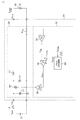
車両灯具の光源の点灯には、スイッチングコンバータが利用される場合が多いが、ADB制御では、光源の点消灯や光量を高速に変化させる必要がある。そこで本発明者は、高速応答性に優れるヒステリシス制御(Bang-Bang制御)を採用することを検討した。図1は、本発明者らが検討したヒステリシス制御の車両用灯具のブロック図である。なおこの比較技術を公知技術として認定してはならない。 A switching converter is often used to turn on the light source of the vehicle lighting equipment, but in ADB control, it is necessary to turn off the light source and change the amount of light at high speed. Therefore, the present inventor has examined the adoption of hysteresis control (Bang-Bang control) having excellent high-speed response. FIG. 1 is a block diagram of a vehicle lamp with hysteresis control examined by the present inventors. This comparative technique must not be certified as a known technique.
車両用灯具1rは、半導体光源10および点灯回路20rを備える。半導体光源10は、LED(発光ダイオード)あるいはLD(レーザダイオード)などの半導体デバイスを含む。点灯回路20rは、スイッチングコンバータ30rおよびコンバータコントローラ32rを含む。 The
スイッチングコンバータ30rは、バッテリ2からスイッチ4を介してバッテリ電圧V BAT(入力電圧VINともいう)を受け、半導体光源10にランプ電流(駆動電流)I LAMPを供給する。たとえばスイッチングコンバータ30rは、降圧コンバータ(Buckコンバータ)であり、入力キャパシタC1、スイッチングトランジスタM1、ダイオードD1、インダクタL1を含む。 The
コンバータコントローラ32rは、ランプ電流ILAMPを検出し、ランプ電流ILA MPが半導体光源10の目標光量に対応する目標電流IREFと一致するように、スイッチングトランジスタM1のスイッチングのデューティ比を調節する。コンバータコントローラ32rはヒステリシス制御方式のコントローラであり、電流検出回路34、ヒステリシスコンパレータ36、ドライバ38を備える。スイッチングコンバータ30rにおいて、ランプ電流ILAMPの経路上には、電流検出抵抗(以下、センス抵抗という)RCSが挿入される。センス抵抗RCSには、ランプ電流ILAMPに比例した電圧降下が発生する。電流検出回路34は、センス抵抗RCSの電圧降下にもとづいて現在のランプ電流ILAMPを示す電流検出信号VCSを生成する。Converter controller 32r detects a lamp current I LAMP, the lamp current I LA MP is to match the target current I REF corresponding to the target light amount of the
ヒステリシスコンパレータ36は、電流検出信号VCSを基準電圧VREFに応じて定まる2つのしきい値信号VTHL,VTHHと比較し、比較結果に応じた制御パルスSC NTを生成する。具体的には制御パルスSCNTは、電流検出信号VCSが、ランプ電流ILAMPのピーク値IPEAKに相当する上側しきい値信号VTHHに達すると第1レベルに遷移し、電流検出信号VCSがランプ電流ILAMPのボトム値IBOTTOMに相当する下側しきい値信号VTHLに達すると第2レベルに遷移する。ドライバ38は、制御パルスSCNTにもとづいてスイッチングトランジスタM1を駆動する。
ランプ電流ILAMPは、ピーク値IPEAKとボトム値IBOTTOMの間を往復することとなり、したがって半導体光源10は、ピーク値IPEAKとボトム値IBOTT OM(2つのしきい値信号VTHH,VTHL)の平均値IREFに応じた輝度で発光する。The lamp current I LAMP becomes a possible back and forth between the peak value I PEAK and the bottom value I BOTTOM, thus the
本発明者らは、上述のヒステリシス制御の点灯回路において、PWM調光(PWM減光)を行うことを検討した。すなわち、制御パルスSCNTの周波数よりも低い周波数のPWM調光パルスSPWMを生成し、PWM調光パルスSPWMが第1レベル(たとえばハイレベル)の点灯期間において、スイッチングトランジスタM1をスイッチングし、第2レベル(たとえばローレベル)の消灯期間において、スイッチングトランジスタM1をオフする。PWM調光パルスSPWMのデューティ比を変化させることにより、半導体光源10の実効的な輝度を変化させることができる。The present inventors have studied performing PWM dimming (PWM dimming) in the above-mentioned hysteresis control lighting circuit. That is, a PWM dimming pulse S PWM having a frequency lower than the frequency of the control pulse S CNT is generated, and the PWM dimming pulse S PWM switches the switching transistor M1 during the lighting period of the first level (for example, high level). The switching transistor M1 is turned off during the extinguishing period of the second level (for example, low level). PWM dimming pulse S By changing the duty ratio of PWM , the effective brightness of the
図2は、図1の車両用灯具1rにおけるPWM調光を説明する図である。なお本明細書において参照する波形図やタイムチャートの縦軸および横軸は、理解を容易とするために適宜拡大、縮小したものであり、また示される各波形も、理解の容易のために簡略化され、あるいは誇張もしくは強調されている。 FIG. 2 is a diagram illustrating PWM dimming in the
PWM調光パルスSPWMがハイレベルに遷移し、点灯期間となると、スイッチングトランジスタM1がターンオンする。そして、ランプ電流ILAMPが、(VIN−VOU T)/Lの傾きで増加していき、上限IPEAKに達すると、スイッチングトランジスタM1がターンオフする。その後、点灯期間の間、ランプ電流ILAMPは、ピーク値IP EAKとボトム値IBOTTOMの間を往復する。PWM dimming pulse S When the PWM transitions to a high level and the lighting period is reached, the switching transistor M1 turns on. Then, the lamp current I LAMP is, increases with a slope of (V IN -V OU T) / L, reaches the limit I PEAK, the switching transistor M1 is turned off. Then, during the lighting period, the lamp current I LAMP reciprocates between the peak value I P EAK and the bottom value I BOTTOM .
やがてPWM調光パルスSPWMがローレベルに遷移し、消灯期間となると、スイッチングトランジスタM1がターンオフする。そうすると、ランプ電流ILAMPが、(VO UT/L)の傾きで低下していき、ゼロとなる。Eventually, the PWM dimming pulse S PWM transitions to a low level, and when the extinguishing period is reached, the switching transistor M1 turns off. Then, the lamp current I LAMP is, continue to decrease a slope of (V O UT / L), it becomes zero.
ヒステリシス制御では、点灯期間と消灯期間の切りかえに際して、ランプ電流ILAM Pが非常に高速に変化する。これはヒステリシス制御の利点のひとつと言える。ところが、インダクタL1のインダクタンスの値や、入出力電圧VIN,VOUTの組み合わせによっては、点灯期間と消灯期間の切りかえ時のランプ電流ILAMPの急峻な変化が、電磁ノイズの原因となり得る。In hysteresis control, upon switching of the lighting period and the off period, the lamp current I LAM P is very rapidly changing. This can be said to be one of the advantages of hysteresis control. However, depending on the value of the inductance of the inductor L1 and the combination of the input / output voltages V IN and V OUT , a sudden change in the lamp current I LAMP at the time of switching between the lighting period and the extinguishing period may cause electromagnetic noise.
本発明はこれらの課題に鑑みてなされたものであり、そのある態様の例示的な目的のひとつは、電磁ノイズを抑制可能な車両用灯具およびその点灯回路の提供にある。 The present invention has been made in view of these problems, and one of the exemplary purposes of the embodiment is to provide a vehicle lamp capable of suppressing electromagnetic noise and a lighting circuit thereof.
本発明のある態様は、車両用灯具に使用される点灯回路に関する。点灯回路は、車両用灯具に設けられた半導体光源に電力を供給するスイッチングコンバータと、スイッチングコンバータを制御するコンバータコントローラと、を備える。コンバータコントローラは、スイッチングコンバータから半導体光源に供給される駆動電流に応じた電流検出信号を、基準信号に応じて定まる上側しきい値信号および下側しきい値信号と比較し、比較結果に応じた制御パルスを生成するヒステリシスコンパレータと、制御パルスに応じてスイッチングコンバータのスイッチングトランジスタを駆動するドライバと、PWM(パルス幅変調)調光信号をなまらせて徐変信号を生成し、徐変信号にもとづいて基準信号を変化させるPWM調光回路と、を備える。 One aspect of the present invention relates to a lighting circuit used in a vehicle lamp. The lighting circuit includes a switching converter that supplies electric power to a semiconductor light source provided in a vehicle lamp, and a converter controller that controls the switching converter. The converter controller compares the current detection signal according to the drive current supplied from the switching converter to the semiconductor light source with the upper threshold signal and the lower threshold signal determined according to the reference signal, and responds to the comparison result. A hysteresis comparator that generates a control pulse, a driver that drives the switching transistor of the switching converter according to the control pulse, and a PWM (pulse width modulation) dimming signal that is blunted to generate a gradual change signal based on the gradual change signal. It is provided with a PWM dimming circuit that changes a reference signal.
この態様によると、ランプ電流の包絡線を、緩やかに変化させることにより、PWM調光にともなう電磁ノイズを抑制できる。 According to this aspect, electromagnetic noise associated with PWM dimming can be suppressed by gently changing the envelope of the lamp current.
PWM調光回路は、PWM調光信号を受け、徐変信号を生成するローパスフィルタ(積分回路)を含んでもよい。これにより、ローパスフィルタのカットオフ周波数(時定数)に応じて、電磁ノイズの量と、PWM調光のリニアリティを調節できる。 The PWM dimming circuit may include a low-pass filter (integration circuit) that receives a PWM dimming signal and generates a gradual change signal. As a result, the amount of electromagnetic noise and the linearity of PWM dimming can be adjusted according to the cutoff frequency (time constant) of the low-pass filter.
ヒステリシスコンパレータは、電流検出信号をしきい値電圧と比較し、制御パルスを生成するコンパレータと、アナログ調光信号が発生するラインと接地の間に順に直列に設けられる第1抵抗、トランジスタおよび第2抵抗と、第1抵抗とトランジスタの接続点に生ずる第1電圧と、トランジスタと第2抵抗の接続点に生ずる第2電圧とを受け、制御パルスに応じた一方を出力するセレクタと、含んでもよい。しきい値電圧は、セレクタの出力電圧に応じていてもよい。 The hysteresis comparator compares the current detection signal with the threshold voltage, generates a control pulse, and provides a first resistor, a transistor, and a second resistor in series between the line where the analog dimming signal is generated and the ground. It may include a resistor, a first voltage generated at the connection point between the first resistor and the transistor, and a second voltage generated at the connection point between the transistor and the second resistor, and a selector that outputs one according to a control pulse. .. The threshold voltage may depend on the output voltage of the selector.
ある態様の点灯回路は、制御パルスの周波数を示す周波数検出信号を生成する周波数検出回路と、周波数検出信号が基準値に近づくように、上側しきい値信号および下側しきい値信号の電位差を変化させるしきい値電圧調節回路と、をさらに備えてもよい。
この態様によると、入力電圧や出力電圧、インダクタンスの変動にかかわらず、スイッチング周波数を基準値に応じた周波数に安定化することができる。A lighting circuit of one embodiment has a potential difference between a frequency detection circuit that generates a frequency detection signal indicating the frequency of a control pulse and an upper threshold signal and a lower threshold signal so that the frequency detection signal approaches a reference value. It may further include a variable threshold voltage control circuit.
According to this aspect, the switching frequency can be stabilized to a frequency corresponding to a reference value regardless of fluctuations in input voltage, output voltage, and inductance.
ある態様の点灯回路は、スイッチングトランジスタのスイッチング周波数より低い周波数の変調信号を生成し、変調信号に応じて上側しきい値信号および下側しきい値信号の差分を変調する変調器をさらに備えてもよい。
この態様によると、スイッチング周波数のスペクトルを拡散させることができ、これにより、ビートノイズなどの発生を抑制できる。The lighting circuit of some embodiment further comprises a modulator that generates a modulated signal at a frequency lower than the switching frequency of the switching transistor and modulates the difference between the upper threshold signal and the lower threshold signal according to the modulated signal. May be good.
According to this aspect, the spectrum of the switching frequency can be diffused, whereby the generation of beat noise and the like can be suppressed.
本発明の別の態様は車両用灯具に関する。車両用灯具は、半導体光源と、半導体光源を点灯させる上述のいずれかの点灯回路と、を備える。 Another aspect of the present invention relates to a vehicle lamp. The vehicle lighting equipment includes a semiconductor light source and any of the above-mentioned lighting circuits for lighting the semiconductor light source.
なお、以上の構成要素の任意の組み合わせや、本発明の構成要素や表現を、方法、装置、システムなどの間で相互に置換したものもまた、本発明の態様として有効である。 It should be noted that any combination of the above components and those in which the components and expressions of the present invention are mutually replaced between methods, devices, systems and the like are also effective as aspects of the present invention.
本発明のある態様によれば、電磁ノイズを抑制できる。 According to an aspect of the present invention, electromagnetic noise can be suppressed.
以下、本発明を好適な実施の形態をもとに図面を参照しながら説明する。各図面に示される同一または同等の構成要素、部材、処理には、同一の符号を付するものとし、適宜重複した説明は省略する。また、実施の形態は、発明を限定するものではなく例示であって、実施の形態に記述されるすべての特徴やその組み合わせは、必ずしも発明の本質的なものであるとは限らない。 Hereinafter, the present invention will be described with reference to the drawings based on preferred embodiments. The same or equivalent components, members, and processes shown in the drawings shall be designated by the same reference numerals, and redundant description will be omitted as appropriate. Further, the embodiment is not limited to the invention but is an example, and all the features and combinations thereof described in the embodiment are not necessarily essential to the invention.
本明細書において、「部材Aが、部材Bと接続された状態」とは、部材Aと部材Bが物理的に直接的に接続される場合のほか、部材Aと部材Bが、それらの電気的な接続状態に実質的な影響を及ぼさない、あるいはそれらの結合により奏される機能や効果を損なわせない、その他の部材を介して間接的に接続される場合も含む。
同様に、「部材Cが、部材Aと部材Bの間に設けられた状態」とは、部材Aと部材C、あるいは部材Bと部材Cが直接的に接続される場合のほか、それらの電気的な接続状態に実質的な影響を及ぼさない、あるいはそれらの結合により奏される機能や効果を損なわせない、その他の部材を介して間接的に接続される場合も含む。In the present specification, the "state in which the member A is connected to the member B" means that the member A and the member B are physically directly connected, and that the member A and the member B are electrically connected to each other. It also includes the case of being indirectly connected via other members, which does not substantially affect the connection state, or does not impair the functions and effects performed by the combination thereof.
Similarly, "a state in which the member C is provided between the member A and the member B" means that the member A and the member C, or the member B and the member C are directly connected, and their electricity. It also includes the case of being indirectly connected via other members, which does not substantially affect the connection state, or does not impair the functions and effects performed by the combination thereof.
また本明細書において、電圧信号、電流信号などの電気信号、あるいは抵抗、キャパシタなどの回路素子に付された符号は、必要に応じてそれぞれの電圧値、電流値、あるいは抵抗値、容量値を表すものとする。 Further, in the present specification, the reference numerals attached to electric signals such as voltage signals and current signals, or circuit elements such as resistors and capacitors have their respective voltage values, current values, resistance values and capacitance values as required. It shall be represented.
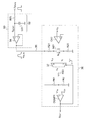
(第1の実施の形態)
図3は、第1の実施の形態に係る車両用灯具1のブロック図である。車両用灯具1は、半導体光源10および点灯回路20を備える。半導体光源10は、LEDやLD、有機EL(エレクトロルミネッセンス)などが例示されるが、特に限定されない。点灯回路20は、スイッチングコンバータ30およびコンバータコントローラ32を備える。図1と同様にスイッチングコンバータ30は降圧コンバータであり、コンバータコントローラ32は、スイッチングコンバータ30から半導体光源10に供給されるランプ電流ILAMPを、所定の目標電流IREFに安定化する。(First Embodiment)
FIG. 3 is a block diagram of the
コンバータコントローラ32は、電流検出回路34、ヒステリシスコンパレータ36、ドライバ38およびPWM調光回路90を備える。電流検出回路34は、スイッチングコンバータ30から半導体光源10に供給されるランプ電流ILAMPに応じた電流検出信号VCSを生成する。図1と同様に、センス抵抗RCSをランプ電流ILAMPの経路上に挿入し、電流検出回路34によりセンス抵抗RCSの電圧降下を増幅して電流検出信号VCSを生成してもよい。The
ヒステリシスコンパレータ36は、電流検出信号VCSを、上側しきい値信号VTHHおよび下側しきい値信号VTHLと比較し、比較結果に応じた制御パルスSCNTを生成する。上側しきい値信号VTHHおよび下側しきい値信号VTHLは、アナログ調光信号VADIMに応じて規定される。
ドライバ38は、制御パルスSCNTに応じてスイッチングコンバータ30のスイッチングトランジスタM1を駆動する。本実施の形態において、制御パルスSCNTのハイレベルがスイッチングトランジスタM1のオンに、ローレベルがスイッチングトランジスタM1のオフに対応する。The
点灯回路20には、PWM調光信号SPWMが入力される。PWM調光信号SPWMは、数十Hz〜数百Hz程度の周波数を有し、そのデューティ比は、半導体光源10の目標輝度に応じて変化する。The PWM dimming signal S PWM is input to the
PWM調光回路90は、PWM調光信号SPWMをなまらせて徐変信号SSOFTを生成し、徐変信号SSOFTにもとづいてアナログ調光信号VADIMを変化させる。
以上が車両用灯具1の構成である。続いてその動作を説明する。図4は、図3の点灯回路20の動作波形図である。アナログ調光信号VADIMは、PWM調光信号SPWMをなまらせた徐変信号に応じた波形を有する。PWM調光信号SPWMがローレベルからハイレベルに遷移し、点灯期間に移行すると、ヒステリシスコンパレータ36における上側しきい値信号VTHHおよび下側しきい値信号VTHLは、アナログ調光信号VADIMに応じて緩やかに増加する。したがって電流検出信号VCS、ひいてはランプ電流ILA MPの包絡線は、アナログ調光信号VADIMに応じて緩やかに増加していく。The above is the configuration of the
反対にPWM調光信号SPWMがハイレベルからローレベルに遷移し、消灯期間に移行すると、ヒステリシスコンパレータ36における上側しきい値信号VTHHおよび下側しきい値信号VTHLは、アナログ調光信号VADIMに応じて緩やかに低下する。したがって電流検出信号VCS、ひいてはランプ電流ILAMPの包絡線は、アナログ調光信号VADIMに応じて緩やかに減少していく。PWM dimming signal S PWM shifts from high level to low level in the opposite, shifting to turn-off period, the upper threshold signal V THH and lower threshold signal V THL in the
以上が点灯回路20の動作である。図4には比較のために、図1におけるランプ電流I LAMP’の波形が一点鎖線で示される。一点鎖線では、PWM調光信号SPWMがハイレベルに遷移すると、ランプ電流ILAMPは直ちに目標電流IREF付近まで増加し、このときの急峻な電流変化が電磁ノイズの要因となる。これに対して図3の点灯回路20によれば、ランプ電流ILAMPは、ILAMP’と傾きこそ同じであるが、1回のスイッチングごとの変化量が小さくなるため、電磁ノイズを抑制できる。 The above is the operation of the
本発明は、図3のブロック図や回路図として把握され、あるいは上述の説明から導かれるさまざまな装置、回路に及ぶものであり、特定の構成に限定されるものではない。以下、本発明の範囲を狭めるためではなく、発明の本質や回路動作の理解を助け、またそれらを明確化するために、より具体的な構成例を説明する。 The present invention extends to various devices and circuits grasped as the block diagram and circuit diagram of FIG. 3 or derived from the above description, and is not limited to a specific configuration. Hereinafter, more specific configuration examples will be described not for narrowing the scope of the present invention, but for helping to understand the essence of the invention and circuit operation, and for clarifying them.
図5は、図3の点灯回路20の一部の構成例を示す回路図である。PWM調光回路90は、ローパスフィルタ92およびバッファ94を含む。ローパスフィルタ92はたとえば1次RCフィルタであり、抵抗R51およびキャパシタC51を含む。ローパスフィルタ92の出力信号が、上述する徐変信号に相当する。バッファ94は、徐変信号を受け、それをアナログ調光信号VADIMとして出力する。バッファ94に代えて、非反転アンプを用いてもよい。FIG. 5 is a circuit diagram showing a partial configuration example of the
アナログ調光信号VADIMを緩やかにしすぎると、電磁ノイズは減少するが、PWM調光信号SPWMのデューティ比が小さい領域において、デューティ比対光強度のリニアリティが悪化する。反対にアナログ調光信号VADIMを急峻にしすぎると、デューティ比対光強度のリニアリティは改善するが電磁ノイズが増加する。図5のPWM調光回路90によれば、ローパスフィルタ92のカットオフ周波数にもとづいて、電磁ノイズの低減効果とPWM調光のリニアリティのバランスを設定できる。If the analog dimming signal V ADIM is made too lenient, the electromagnetic noise is reduced, but the linearity of the duty ratio to the light intensity deteriorates in the region where the duty ratio of the PWM dimming signal S PWM is small. On the contrary, if the analog dimming signal VADIM is made too steep, the linearity of the duty ratio to the light intensity is improved, but the electromagnetic noise increases. According to the
ヒステリシスコンパレータ36は、コンパレータCOMP1、第1抵抗R21、第2抵抗R22、第1トランジスタM21、セレクタ37、抵抗R61〜R63を含む。コンパレータCOMP1は、電流検出信号VCSをしきい値電圧VTHと比較し、制御パルスS CNTを生成する。第1抵抗R21、第1トランジスタM21、第2抵抗R22は、アナログ調光信号VADIMが発生するライン96と接地の間に順に直列に設けられる。 The
第1トランジスタM21のゲートは適切にバイアスされる。たとえば第1トランジスタM21のバイアスのためにオペアンプOA1が設けられる。オペアンプOA1の出力は、第1トランジスタM21のゲートと接続され、非反転入力端子には、トランジスタM21と第2抵抗R22の接続点と接続され、反転入力端子にはとある電圧VXが入力される。この構成では、第1トランジスタM21に、電圧VXに比例した電流IX=VX/R22が流れるようにバイアスされる。このとき、2つの電圧VH,VLは以下の式で表される。
VH=VADIM−Ix×R21 …(1a)
VL=Ix×R22 …(1b)
R21=R22=Rとすれば、
VH=VADIM−Ix×R …(2a)
VL=Ix×R …(2b)
となる。またそれらの平均電圧は、式(3)で与えられる。
(VH+VL)/2=VADIM/2 …(3)
つまり、ランプ電流ILAMPの平均値(IREF)をアナログ調光電圧VADIMにもとづいて制御することができる。The gate of the first transistor M21 is properly biased. For example, the operational amplifier OA1 is provided for the bias of the first transistor M21. The output of the operational amplifier OA1 is connected to the gate of the first transistor M21, the non-inverting input terminal is connected to the connection point between the transistor M21 and the second resistor R22, and a certain voltage V X is input to the inverting input terminal. To. In this configuration, the first transistor M21 is biased so that a current IX = V X / R 22 proportional to the voltage V X flows. At this time, the two voltages V H and VL are expressed by the following equations.
V H = V ADIM −Ix × R21… (1a)
VL = Ix × R22… (1b)
If R21 = R22 = R, then
V H = V ADIM −Ix × R… (2a)
VL = Ix × R ... (2b)
Will be. The average voltage thereof is given by the equation (3).
(V H + VL ) / 2 = V ADIM / 2 ... (3)
That is, the average value (I REF ) of the lamp current I LAMP can be controlled based on the analog dimming voltage V ADIM .
セレクタ37は、第1抵抗R21と第1トランジスタM21の接続点に生ずる第1電圧VHと、第1トランジスタM21と第2抵抗R22の接続点に生ずる第2電圧VLとを受け、制御パルスSCNTに応じた一方を出力する。The
コンパレータCOMP1に与えられるしきい値電圧VTHは、セレクタ37の出力電圧VYに応じている。たとえば抵抗R61〜R63によって、電圧VYおよびアナログ調光信号VADIMを加算平均して、しきい値電圧VTHを生成してもよい。あるいは電圧V Yをそのまましきい値電圧VTHとしてもよい。 Threshold voltage V given to comparator COMP1THIs the output voltage V of the
(第2の実施の形態)
図6は、第2の実施の形態に係る車両用灯具1aのブロック図である。図6のコンバータコントローラ32aは、図3のコンバータコントローラ32に加えて、周波数検出回路40およびしきい値電圧調節回路42をさらに備える。(Second Embodiment)
FIG. 6 is a block diagram of the
周波数検出回路40は、制御パルスSCNTの周波数、つまりスイッチングトランジスタM1のスイッチング周波数を示す周波数検出信号VFREQを生成する。しきい値電圧調節回路42は、周波数検出信号VFREQが基準値VREFに近づくように、上側しきい値信号VTHHおよび下側しきい値信号VTHLの電位差(ヒステリシス幅)ΔV(=VTHH−VTHL)を変化させる。The
第2の実施の形態によれば、入力電圧VINや出力電圧VOUT、インダクタンスL1の変動にかかわらず、スイッチング周波数を基準値VREFに応じた周波数に安定化することができる。According to the second embodiment, the switching frequency can be stabilized to a frequency corresponding to the reference value V REF regardless of fluctuations in the input voltage V IN , the output voltage V OUT , and the inductance L1.
続いて第2の実施の形態の具体的な構成例を説明する。図7は、図6の点灯回路20aの構成例を示す回路図である。図7には、周波数検出回路40、しきい値電圧調節回路42およびヒステリシスコンパレータ36の一部が示されている。 Subsequently, a specific configuration example of the second embodiment will be described. FIG. 7 is a circuit diagram showing a configuration example of the
周波数検出回路40は、F/V変換回路と把握することができる。周波数検出回路40は、ハイパスフィルタ52、第1キャパシタC11、第2トランジスタM12、充電回路54、ピークホールド回路56を含む。ハイパスフィルタ52は、制御パルスSCNTもしくはスイッチングトランジスタM1のゲートパルスを受ける。ハイパスフィルタ52は微分回路と把握することもできる。第1キャパシタC11の一端は接地される。充電回路54は、第1キャパシタC11を充電する。充電回路54は、電流源あるいは抵抗で構成される。第2トランジスタM12は第1キャパシタC11と並列に接続され、ハイパスフィルタ52の出力信号が、ゲートソース間しきい値電圧を超えると第1キャパシタC11を放電する。The
第1キャパシタC11には、ランプ波形を有する第1周期信号S11が発生する。周波数検出回路40は、第1周期信号S11の振幅に応じた周波数検出信号VFREQを出力する。具体的にはピークホールド回路56は、第1周期信号S11を受け、そのピーク値を示す周波数検出信号VFREQを出力する。なお周波数検出回路40の構成は特に限定されない。A first period signal S11 having a lamp waveform is generated in the first capacitor C11. The
上述したように図5のヒステリシスコンパレータ36において、2つの電圧VH,VLは式(2a)、(2b)で与えられる。したがってそれらの電位差は、式(4)で与えられる。
VH−VL=VADIM−2×Ix×R=VADIM−2×VX …(4)
したがって、電圧VXを変化させることにより、電位差VH−VLを変化が変化し、ひいてはヒステリシス幅ΔVを変化させることができる。As described above, in the
V H- V L = V ADIM -2 x Ix x R = V ADIM -2 x V X ... (4)
Therefore, by changing the voltage V X , the change in the potential difference V H - VL can be changed, and thus the hysteresis width ΔV can be changed.
そこでしきい値電圧調節回路42は、周波数検出信号VFREQが基準値VREFに近づくように、電圧VXを変化させる。たとえばしきい値電圧調節回路42は、周波数検出信号VFREQと基準値VREFの誤差にもとづいて電圧VXを生成してもよい。しきい値電圧調節回路42は、周波数検出信号VFREQを基準値VREFと比較する電圧コンパレータと、電圧コンパレータの出力パルスを平滑化するローパスフィルタと、を含んでもよい。あるいはしきい値電圧調節回路42は、周波数検出信号VFREQと基準値VR EFの誤差を増幅するエラーアンプを含んでもよい。Therefore, the threshold
図7の回路動作を説明する。スイッチングトランジスタM1のスイッチング周波数が目標周波数より高い状態では、VFREQ<VREFとなり、電圧VXが低下する。これにより、上側電圧VHと下側電圧VLの電位差つまりしきい値電圧VTHH、VTHLの電位差ΔVが大きくなり、スイッチング周波数が低くなる方向、つまり目標周波数に近づく方向にフィードバックがかかる。The circuit operation of FIG. 7 will be described. When the switching frequency of the switching transistor M1 is higher than the target frequency, V FEQU <V REF , and the voltage V X drops. Thus, the potential difference, i.e. the threshold voltage V THH the upper voltage V H and the lower voltage V L, V THL of the potential difference ΔV is increased, the direction in which the switching frequency is low, the feedback that is toward the target frequency such.
反対に、スイッチングトランジスタM1のスイッチング周波数が目標周波数より低い状態では、VFREQ>VREFとなり、電圧VXが上昇する。これにより、上側電圧VHと下側電圧VLの電位差が小さくなり、スイッチング周波数が高くなる方向、つまり目標周波数に近づく方向にフィードバックがかかる。このようにして点灯回路20によれば、スイッチング周波数を目標周波数に安定化することができる。On the contrary, when the switching frequency of the switching transistor M1 is lower than the target frequency, V FEQU > V REF , and the voltage V X rises. As a result, the potential difference between the upper voltage V H and the lower voltage VL becomes smaller, and feedback is applied in the direction in which the switching frequency becomes higher, that is, in the direction closer to the target frequency. In this way, according to the
周波数のフィードバック制御は、入力電圧VINの変動に限らず、出力電圧VOUTの変動、インダクタL1のインダクタンスのばらつき、温度変動など、スイッチング周波数を変動させるあらゆる変動、ばらつきに対して有効である。そしてスイッチング周波数の予期せぬ変動を抑制できるため、スイッチングノイズ対策にかかるコストを削減することが可能である。The frequency feedback control is effective not only for fluctuations in the input voltage V IN but also for fluctuations in the output voltage V OUT , variations in the inductance of the inductor L1, variations in temperature, and all other fluctuations and variations in the switching frequency. Since it is possible to suppress unexpected fluctuations in the switching frequency, it is possible to reduce the cost of countermeasures against switching noise.
また、上側しきい値信号VTHHと下側しきい値信号VTHLの平均レベルは、アナログ調光信号VADIMのみに依存しており、ヒステリシス幅Vxには依存しない。したがってヒステリシス幅ΔVを変化させつつも、ランプ電流ILAMPの平均値を一定に維持することができ、半導体光源10のちらつきを防止できる。The average level of the upper threshold signal V THH and the lower threshold signal V THL is dependent only on the analog dimming signal V ADIM, not on the hysteresis width Vx. Therefore, the average value of the lamp current I LAMP can be kept constant while changing the hysteresis width ΔV, and the flicker of the
(第3の実施の形態)
図8は、第3の実施の形態に係る車両用灯具1bのブロック図である。図6のコンバータコントローラ32bは、図6のコンバータコントローラ32aに加えて、変調器60をさらに備える。変調器60は、スイッチングトランジスタM1のスイッチング周波数より低い周波数の変調信号VMODを生成し、変調信号VMODに応じて上側しきい値信号V THHおよび下側しきい値信号VTHLの差分(ヒステリシス幅)を変調する。たとえば変調器60は、しきい値電圧調節回路42に入力される基準値VREFに変調信号VMO Dを重畳してもよい。(Third Embodiment)
FIG. 8 is a block diagram of the
図9は、変調器60の構成例を示す回路図である。変調器60は、スイッチング周波数よりも十分に周波数が低い変調信号VMODを生成する発振器62を含み、変調信号VM ODに応じて、基準値VREFを変化させる。発振器62は、抵抗R91〜R94、キャパシタC91、オペアンプOA91を含む。キャパシタC91には、抵抗R91,R92により定まる電圧レベルを基準とした三角波の変調信号VMODが発生する。FIG. 9 is a circuit diagram showing a configuration example of the
なお変調信号VMODの波形は特に限定されず、のこぎり波、ランプ波、正弦波、台形波のいずれかであってもよく、別の観点から言えば、スロープを有する周期信号であればよい。抵抗R95〜R97によって、変調信号VMODと電源電圧VCCが、加算平均(重み付け加算)され、変調信号VMODが重畳された基準値VREFが生成される。The waveform of the modulated signal V MOD is not particularly limited, and may be a sawtooth wave, a ramp wave, a sine wave, or a trapezoidal wave. From another point of view, it may be a periodic signal having a slope. The resistance R95~R97, modulated signal V MOD and the power supply voltage V CC is, are averaged (weighted addition), the reference value V REF to the modulation signal V MOD is superimposed is generated.
第3の実施の形態によれば、スイッチング周波数の目標周波数を、変調信号VMODに応じてゆっくりと変化させながら、実際のスイッチング周波数を目標周波数に近づけるようにフィードバック制御することにより、入力電圧VINや出力電圧VOUTの変動、インダクタンスのばらつき、温度変動等の影響を排除しつつも、スイッチング周波数のスペクトルを拡散させることができる。これにより、ビートノイズなどの発生を抑制できる。According to the third embodiment, the input voltage V is controlled by feedback-controlling the target frequency of the switching frequency so as to bring the actual switching frequency closer to the target frequency while slowly changing the target frequency according to the modulation signal V MOD. It is possible to diffuse the spectrum of the switching frequency while eliminating the effects of fluctuations in IN and output voltage V OUT , fluctuations in inductance, fluctuations in temperature, and the like. As a result, the generation of beat noise and the like can be suppressed.
なお第3の実施の形態において、変調器60に要求される機能は、変調信号VMODに応じて上側しきい値信号VTHHおよび下側しきい値信号VTHLの差分ΔVを変調することである。したがって変調器60は、基準値VREFに代えて周波数検出信号VFRE Qに対して、変調信号VMODを重畳してもよい。In yet a third embodiment, functions required to the
(第4の実施の形態)
図10は、第4の実施の形態に係る車両用灯具1cのブロック図である。図10のコンバータコントローラ32cは、図3のコンバータコントローラ32に加えて変調器70を備える。変調器70は、スイッチングトランジスタM1のスイッチング周波数よりも低い周波数の変調信号VMODを生成し、変調信号VMODに応じてヒステリシス幅ΔVを変調する。変調器70は、図9の変調器60と同様に構成してもよい。(Fourth Embodiment)
FIG. 10 is a block diagram of the
ヒステリシスコンパレータ36を、図5の構成とする場合、トランジスタM21のバイアス状態つまり電流Ixを、変調信号VMODにもとづいて変調すればよい。上述のように電圧VHとVLの電位差すなわちヒステリシス幅ΔVは、式(4)で与えられる。したがって、電圧Vxに変調信号VMODを重畳することにより、ヒステリシス幅ΔVを変調し、スペクトルを拡散することができる。A
(変形例)
続いて、いくつかの実施の形態において適用可能な変形例を説明する。(Modification example)
Subsequently, a modification applicable to some embodiments will be described.
(第1変形例)
いくつかの実施の形態では、PWM調光回路90、周波数検出回路40、しきい値電圧調節回路42、変調器70、等をアナログ回路で構成したが、それらの一部あるいは全部をデジタル回路で構成してもよい。さらには、コンバータコントローラ32全体をデジタル回路をベースに構成してもよい。この場合、電流検出回路34の出力信号をデジタル値に変換するA/Dコンバータを追加し、ヒステリシスコンパレータ36をデジタルコンパレータとすればよい。(First modification)
In some embodiments, the
(第2変形例)
スイッチングコンバータ30は昇圧コンバータ、昇降圧コンバータであってもよいし、トランスを用いたコンバータであってもよいし、Cukコンバータなどその他のコンバータであってもよい。(Second modification)
The switching
(用途)
図11は、ADB機能を有するアレイ方式の車両用灯具1のブロック図である。ADBにおいては、ハイビーム照射領域は、複数N個(Nは2以上の自然数)のサブ領域に分割される。半導体光源10は、N個のサブ領域に対応づけられる複数の発光素子12_1〜12_Nを含む。各発光素子12は、LED(発光ダイオード)やLD(レーザダイオード)などの半導体デバイスであり、それぞれが対応するサブ領域を照射するよう配置される。点灯回路20は、複数の発光素子12_1〜12_Nそれぞれのオン(点灯)、オフ(消灯)を制御することで、ハイビームの配光を変化させる。あるいは点灯回路20は、高い周波数で発光素子12をPWM(パルス幅変調)制御することで、実効的な輝度を調節する。(Use)
FIG. 11 is a block diagram of an array
点灯回路20は、スイッチングコンバータ30および図示しないコンバータコントローラ32に加えて、複数のバイパス回路80_1〜80_N、コントローラ82を備える。複数のバイパス回路80_1〜80_Nは、複数の発光素子12_1〜12_Nに対応づけられる。バイパス回路80はオン、オフが切りかえ可能に構成される。i番目のバイパス回路80_iがオン状態となると、ランプ電流ILAMPが、発光素子12_iではなくバイパス回路80_iに流れ、発光素子12_iが消灯し、バイパス回路80_iがオフ状態となると、ランプ電流ILAMPが発光素子12_iに流れて点灯する。The
車両用灯具1を制御する上流のプロセッサ(たとえば電子制御ユニットECU)6は、車両前方の状態にもとづいて、ハイビームにより照射すべきサブ領域を判定し、点灯回路20のコントローラ82に指示する。コントローラ82は、プロセッサ6からの制御指令にもとづいてバイパス回路80_1〜80_Nの状態を制御する。具体的には、照射すべきサブ領域に対応する発光素子12を選択し、選択された発光素子12と並列なバイパス回路80をオフ状態とし、残りの発光素子12と並列なバイパス回路80をオン状態とする。 The upstream processor (for example, the electronic control unit ECU) 6 that controls the
図12は、ADB機能を有するブレードスキャン方式の車両用灯具1を模式的に示す斜視図である。車両用灯具1は主として、走査型光源11、投影レンズ120および点灯回路20を備える。 FIG. 12 is a perspective view schematically showing a blade scan
走査型光源11は、ブレード(反射鏡)100および光源10を備える。光源10は複数個設けてもよいが、ここでは理解の容易化、説明の簡素化のため、1個の光源10の場合を説明する。 The
光源10は、LED(発光ダイオード)あるいはレーザダイオードを利用した半導体光源である。ブレード100は光源10の出射光L1を受け、所定の周期運動を繰り返すことによりその反射光L2を車両前方で横方向(図中、Y方向)に走査する。本実施の形態では、ブレード100は、図示しないモータに取り付けられており、回転運動を行なう。ある時刻においてブレード100の出射光L1は、ブレード100の位置(ロータの回転角)に応じた反射角で反射し、照射領域300が形成される。 The
ブレード100が回転することで、反射角が変化し、照射領域300がY方向に走査される。この動作を高速に、たとえば50Hz以上で繰り返すことで車両前方には、配光パターン310が形成される。点灯回路20は、所望の配光パターンが得られるように、ブレード100の周期運動と同期しながら、光源10の光量(輝度)を制御する。照射領域300が照射される範囲(領域)を点灯領域RON、照射領域300が照射されない範囲(領域)を消灯領域ROFFと称する。配光パターン310は、点灯領域RONと消灯領域ROFFの組み合わせである。As the
図12の車両用灯具1において、前方車両に対するアンチグレアのために、前方車両の存在箇所を消灯領域ROFFとする配光パターン310を形成する場合を考える。この場合、半導体光源10の点消灯は、ブレード100の周期運動と同期して切りかえられ、したがってこの動作もPWM調光の一種と捉えることができる。Consider a case where the
走査型光源11の構成は図12のそれに限定されない。たとえばブレード100に代えて、ポリゴンミラーやガルバノミラーを用いてもよいし、MEMS(Micro Electro Mechanical Systems)スキャンミラーを用いてもよい。また、モータに代えてアクチュエータを設け、ブレード100の向きを変化させてもよい。 The configuration of the
あるいはブレード100を固定し、あるいは省略して、半導体光源10の光軸をアクチュエータによって移動させてもよい。あるいはブレード100に代えて、電気光学素子を利用してもよい。たとえば電気光学素子は屈折率が電圧あるいは電流、温度等によって制御可能なレンズであってもよい。周期的にレンズの屈折率を変化させることにより、光を走査させてもよい。 Alternatively, the
実施の形態にもとづき、具体的な語句を用いて本発明を説明したが、実施の形態は、本発明の原理、応用を示しているにすぎず、実施の形態には、請求の範囲に規定された本発明の思想を逸脱しない範囲において、多くの変形例や配置の変更が認められる。 Although the present invention has been described using specific terms and phrases based on the embodiments, the embodiments merely indicate the principles and applications of the present invention, and the embodiments are defined in the claims. Many modifications and arrangement changes are permitted without departing from the ideas of the present invention.
1…車両用灯具、2…バッテリ、4…スイッチ、6…プロセッサ、10…半導体光源、12…発光素子、20…点灯回路、30…スイッチングコンバータ、32…コンバータコントローラ、34…電流検出回路、36…ヒステリシスコンパレータ、COMP1…コンパレータ、37…セレクタ、38…ドライバ、M1…スイッチングトランジスタ、D1…ダイオード、L1…インダクタ、C1…入力キャパシタ、OA1…オペアンプ、R21…第1抵抗、R22…第2抵抗、M21…第1トランジスタ、40…周波数検出回路、42…しきい値電圧調節回路、60…変調器、62…発振器、70…変調器、90…PWM調光回路。1 ... Vehicle lighting, 2 ... Battery, 4 ... Switch, 6 ... Processor, 10 ... Semiconductor light source, 12 ... Light emitting element, 20 ... Lighting circuit, 30 ... Switching converter, 32 ... Converter controller, 34 ... Current detection circuit, 36 ... Hysteresis comparator, COMP1 ... Comparator, 37 ... Selector, 38 ... Driver, M1 ... Switching transistor, D1 ... Diode, L1 ... inductor, C1 ... Input capacitor, OA1 ... Operational amplifier, R21 ... 1st resistor, R22 ... 2nd resistor, M21 ... 1st transistor, 40 ... frequency detection circuit, 42 ... threshold voltage adjustment circuit, 60 ... modulator, 62 ... oscillator, 70 ... modulator, 90 ... PWM dimming circuit.
本発明は照明等に利用できる。 The present invention can be used for lighting and the like.
Claims (6)
前記スイッチングコンバータを制御するコンバータコントローラと、
を備え、
前記コンバータコントローラは、
前記スイッチングコンバータから前記半導体光源に供給されるランプ電流に応じた電流検出信号を、アナログ調光信号に応じて定まる上側しきい値信号および下側しきい値信号と比較し、比較結果に応じた制御パルスを生成するヒステリシスコンパレータと、
前記制御パルスに応じて前記スイッチングコンバータのスイッチングトランジスタを駆動するドライバと、
PWM(パルス幅変調)調光信号のエッジをなまらせてパルス状の徐変信号を生成し、前記徐変信号に応じた波形を有する前記アナログ調光信号を生成するPWM調光回路と、
を備えることを特徴とする点灯回路。 A switching converter that supplies power to a semiconductor light source,
A converter controller that controls the switching converter and
With
The converter controller
The current detection signal corresponding to the lamp current supplied from the switching converter to the semiconductor light source was compared with the upper threshold signal and the lower threshold signal determined according to the analog dimming signal, and the comparison result was obtained. A hysteresis comparator that generates a control pulse and
A driver that drives the switching transistor of the switching converter in response to the control pulse,
And PWM dimming circuit PWM and blunted the edge of the (Pulse Width Modulation) dimming signal to generate a pulsed gradual change signal to generate said analog dimming signal having a waveform corresponding to the gradual change signal,
A lighting circuit characterized by being provided with.
前記電流検出信号をしきい値電圧と比較し、前記制御パルスを生成するコンパレータと、
前記アナログ調光信号が発生するラインと接地の間に順に直列に設けられる第1抵抗、トランジスタおよび第2抵抗と、
前記第1抵抗と前記トランジスタの接続点に生ずる第1電圧と、前記トランジスタと前記第2抵抗の接続点に生ずる第2電圧とを受け、前記制御パルスに応じた一方を出力するセレクタと、
含み、前記しきい値電圧は、前記セレクタの出力電圧に応じていることを特徴とする請求項1または2に記載の点灯回路。 The hysteresis comparator is
A comparator that compares the current detection signal with the threshold voltage and generates the control pulse,
A first resistor, a transistor, and a second resistor provided in series between the line where the analog dimming signal is generated and the ground are
A selector that receives the first voltage generated at the connection point between the first resistor and the transistor and the second voltage generated at the connection point between the transistor and the second resistor and outputs one according to the control pulse.
The lighting circuit according to claim 1 or 2, wherein the threshold voltage includes and corresponds to the output voltage of the selector.
前記周波数検出信号が基準値に近づくように、前記上側しきい値信号および前記下側しきい値信号の電位差を変化させるしきい値電圧調節回路と、
をさらに備えることを特徴とする請求項1から3のいずれかに記載の点灯回路。 A frequency detection circuit that generates a frequency detection signal indicating the frequency of the control pulse, and
A threshold voltage adjusting circuit that changes the potential difference between the upper threshold signal and the lower threshold signal so that the frequency detection signal approaches a reference value.
The lighting circuit according to any one of claims 1 to 3, further comprising.
前記半導体光源を点灯させる請求項1から5のいずれかに記載の点灯回路と、
を備えることを特徴とする車両用灯具。 With a semiconductor light source
The lighting circuit according to any one of claims 1 to 5, which lights the semiconductor light source.
A vehicle lighting fixture characterized by being equipped with.
Applications Claiming Priority (3)
| Application Number | Priority Date | Filing Date | Title |
|---|---|---|---|
| JP2016041377 | 2016-03-03 | ||
| JP2016041377 | 2016-03-03 | ||
| PCT/JP2017/006743 WO2017150322A1 (en) | 2016-03-03 | 2017-02-23 | Vehicle lamp fixture and lighting circuit for same |
Publications (2)
| Publication Number | Publication Date |
|---|---|
| JPWO2017150322A1 JPWO2017150322A1 (en) | 2018-12-27 |
| JP6820909B2 true JP6820909B2 (en) | 2021-01-27 |
Family
ID=59743879
Family Applications (1)
| Application Number | Title | Priority Date | Filing Date |
|---|---|---|---|
| JP2018503083A Active JP6820909B2 (en) | 2016-03-03 | 2017-02-23 | Vehicle lighting fixtures and their lighting circuits |
Country Status (5)
| Country | Link |
|---|---|
| US (1) | US10710495B2 (en) |
| EP (1) | EP3426009A4 (en) |
| JP (1) | JP6820909B2 (en) |
| CN (1) | CN108781495B (en) |
| WO (1) | WO2017150322A1 (en) |
Families Citing this family (9)
| Publication number | Priority date | Publication date | Assignee | Title |
|---|---|---|---|---|
| CN109219920B (en) * | 2016-06-13 | 2021-08-10 | 株式会社小糸制作所 | Load driving device and vehicle lamp |
| WO2018047915A1 (en) * | 2016-09-09 | 2018-03-15 | 株式会社小糸製作所 | Lighting circuit, vehicle lamp, and driving method for light source |
| CA3019815A1 (en) * | 2017-10-11 | 2019-04-11 | Yourtruckshop Inc. | Truck headlight circuit |
| IL255585B (en) * | 2017-11-09 | 2021-01-31 | Zak Alexander | Battery-powered current regulator for pulsed loads |
| US10686379B2 (en) | 2018-02-06 | 2020-06-16 | Linear Technology Holding, LLC | Load current feedforward schemes for current-mode controlled power converters |
| TWI658282B (en) * | 2018-04-16 | 2019-05-01 | 緯創資通股份有限公司 | Detecting device and detecting method |
| US10728985B2 (en) | 2018-10-16 | 2020-07-28 | Koito Manufacturing Co., Ltd. | Vehicle lamp and lighting circuit |
| JP7411068B2 (en) | 2020-03-24 | 2024-01-10 | ローム株式会社 | Light emission control device, light emitting device and vehicle |
| CN111443629B (en) * | 2020-04-02 | 2021-09-10 | 南京理工大学 | Power supply and control circuit applied to cube star brake sail |
Family Cites Families (9)
| Publication number | Priority date | Publication date | Assignee | Title |
|---|---|---|---|---|
| CN102037783B (en) * | 2008-01-30 | 2013-05-08 | Nxp股份有限公司 | Method and circuit arrangement for regulating LED current flowing through LED circuit arrangement, and associated circuit composition and lighting system |
| JP5645741B2 (en) * | 2011-04-18 | 2014-12-24 | 三菱電機株式会社 | Power supply device and lighting device |
| JP6030922B2 (en) * | 2012-06-11 | 2016-11-24 | 株式会社小糸製作所 | Light source control device |
| US8680781B1 (en) * | 2012-09-07 | 2014-03-25 | Infineon Technologies Austria Ag | Circuit and method for driving LEDs |
| US8803445B2 (en) * | 2012-09-07 | 2014-08-12 | Infineon Technologies Austria Ag | Circuit and method for driving LEDs |
| JP6147073B2 (en) | 2013-04-30 | 2017-06-14 | 株式会社小糸製作所 | Control unit and vehicle lamp |
| CN104202876B (en) * | 2014-09-01 | 2016-10-05 | 矽力杰半导体技术(杭州)有限公司 | The LED drive circuit of a kind of single inductance and driving method |
| JP6489347B2 (en) * | 2014-09-10 | 2019-03-27 | パナソニックIpマネジメント株式会社 | Light emitting element lighting device, light emitting module, and lighting device |
| US9554440B2 (en) * | 2014-10-13 | 2017-01-24 | Seoul Semiconductor Co., Ltd. | Dimmable LED lighting apparatus |
-
2017
- 2017-02-23 JP JP2018503083A patent/JP6820909B2/en active Active
- 2017-02-23 CN CN201780014894.1A patent/CN108781495B/en active Active
- 2017-02-23 WO PCT/JP2017/006743 patent/WO2017150322A1/en active Application Filing
- 2017-02-23 EP EP17759788.7A patent/EP3426009A4/en not_active Withdrawn
-
2018
- 2018-08-30 US US16/117,962 patent/US10710495B2/en active Active
Also Published As
| Publication number | Publication date |
|---|---|
| EP3426009A4 (en) | 2019-10-09 |
| JPWO2017150322A1 (en) | 2018-12-27 |
| US20190016249A1 (en) | 2019-01-17 |
| EP3426009A1 (en) | 2019-01-09 |
| CN108781495B (en) | 2021-04-13 |
| CN108781495A (en) | 2018-11-09 |
| WO2017150322A1 (en) | 2017-09-08 |
| US10710495B2 (en) | 2020-07-14 |
Similar Documents
| Publication | Publication Date | Title |
|---|---|---|
| JP6820909B2 (en) | Vehicle lighting fixtures and their lighting circuits | |
| JP6726668B2 (en) | Lighting circuit for vehicle lamp and light source | |
| JP6396160B2 (en) | Vehicle lamp and its lighting circuit | |
| US10000150B2 (en) | Lighting circuit and vehicle lamp | |
| JP6782228B2 (en) | Vehicle lighting | |
| JP6899710B2 (en) | Vehicle lighting | |
| JP6872413B2 (en) | Vehicle lighting | |
| CN108882438B (en) | Driving circuit and vehicle lamp | |
| JP7183018B2 (en) | Lighting circuit and vehicle lamp | |
| JP6916668B2 (en) | Lighting circuit for vehicle lighting equipment and light source | |
| JP6767860B2 (en) | Converter controller and vehicle lighting | |
| JP6916649B2 (en) | Lighting circuit and vehicle lighting equipment | |
| US10993297B2 (en) | Lighting circuit and vehicular lamp | |
| WO2022131303A1 (en) | Vehicle lamp and illumination method | |
| CN107771413B (en) | Vehicle headlight | |
| JP6889612B2 (en) | Lighting circuit for vehicle lamps and light sources | |
| WO2022091974A1 (en) | Vehicle lamp | |
| JP6826381B2 (en) | Lighting circuit for vehicle lighting equipment and light source | |
| WO2022131302A1 (en) | Vehicle lamp |
Legal Events
| Date | Code | Title | Description |
|---|---|---|---|
| A621 | Written request for application examination |
Free format text: JAPANESE INTERMEDIATE CODE: A621 Effective date: 20191118 |
|
| A131 | Notification of reasons for refusal |
Free format text: JAPANESE INTERMEDIATE CODE: A131 Effective date: 20200714 |
|
| A521 | Request for written amendment filed |
Free format text: JAPANESE INTERMEDIATE CODE: A523 Effective date: 20200911 |
|
| TRDD | Decision of grant or rejection written | ||
| A01 | Written decision to grant a patent or to grant a registration (utility model) |
Free format text: JAPANESE INTERMEDIATE CODE: A01 Effective date: 20201208 |
|
| A61 | First payment of annual fees (during grant procedure) |
Free format text: JAPANESE INTERMEDIATE CODE: A61 Effective date: 20210105 |
|
| R150 | Certificate of patent or registration of utility model |
Ref document number: 6820909 Country of ref document: JP Free format text: JAPANESE INTERMEDIATE CODE: R150 |