JP6790416B2 - Light emitting device - Google Patents
Light emitting device Download PDFInfo
- Publication number
- JP6790416B2 JP6790416B2 JP2016070432A JP2016070432A JP6790416B2 JP 6790416 B2 JP6790416 B2 JP 6790416B2 JP 2016070432 A JP2016070432 A JP 2016070432A JP 2016070432 A JP2016070432 A JP 2016070432A JP 6790416 B2 JP6790416 B2 JP 6790416B2
- Authority
- JP
- Japan
- Prior art keywords
- light emitting
- convex portion
- resin frame
- emitting device
- lead
- Prior art date
- Legal status (The legal status is an assumption and is not a legal conclusion. Google has not performed a legal analysis and makes no representation as to the accuracy of the status listed.)
- Active
Links
Images


Classifications
-
- H—ELECTRICITY
- H10—SEMICONDUCTOR DEVICES; ELECTRIC SOLID-STATE DEVICES NOT OTHERWISE PROVIDED FOR
- H10W—GENERIC PACKAGES, INTERCONNECTIONS, CONNECTORS OR OTHER CONSTRUCTIONAL DETAILS OF DEVICES COVERED BY CLASS H10
- H10W90/00—Package configurations
-
- H—ELECTRICITY
- H10—SEMICONDUCTOR DEVICES; ELECTRIC SOLID-STATE DEVICES NOT OTHERWISE PROVIDED FOR
- H10H—INORGANIC LIGHT-EMITTING SEMICONDUCTOR DEVICES HAVING POTENTIAL BARRIERS
- H10H20/00—Individual inorganic light-emitting semiconductor devices having potential barriers, e.g. light-emitting diodes [LED]
- H10H20/80—Constructional details
- H10H20/85—Packages
- H10H20/857—Interconnections, e.g. lead-frames, bond wires or solder balls
-
- H—ELECTRICITY
- H10—SEMICONDUCTOR DEVICES; ELECTRIC SOLID-STATE DEVICES NOT OTHERWISE PROVIDED FOR
- H10H—INORGANIC LIGHT-EMITTING SEMICONDUCTOR DEVICES HAVING POTENTIAL BARRIERS
- H10H20/00—Individual inorganic light-emitting semiconductor devices having potential barriers, e.g. light-emitting diodes [LED]
- H10H20/80—Constructional details
- H10H20/85—Packages
- H10H20/8506—Containers
-
- H—ELECTRICITY
- H10—SEMICONDUCTOR DEVICES; ELECTRIC SOLID-STATE DEVICES NOT OTHERWISE PROVIDED FOR
- H10H—INORGANIC LIGHT-EMITTING SEMICONDUCTOR DEVICES HAVING POTENTIAL BARRIERS
- H10H20/00—Individual inorganic light-emitting semiconductor devices having potential barriers, e.g. light-emitting diodes [LED]
- H10H20/80—Constructional details
- H10H20/85—Packages
- H10H20/852—Encapsulations
- H10H20/853—Encapsulations characterised by their shape
-
- H—ELECTRICITY
- H10—SEMICONDUCTOR DEVICES; ELECTRIC SOLID-STATE DEVICES NOT OTHERWISE PROVIDED FOR
- H10H—INORGANIC LIGHT-EMITTING SEMICONDUCTOR DEVICES HAVING POTENTIAL BARRIERS
- H10H20/00—Individual inorganic light-emitting semiconductor devices having potential barriers, e.g. light-emitting diodes [LED]
- H10H20/80—Constructional details
- H10H20/85—Packages
- H10H20/852—Encapsulations
- H10H20/854—Encapsulations characterised by their material, e.g. epoxy or silicone resins
-
- H—ELECTRICITY
- H10—SEMICONDUCTOR DEVICES; ELECTRIC SOLID-STATE DEVICES NOT OTHERWISE PROVIDED FOR
- H10H—INORGANIC LIGHT-EMITTING SEMICONDUCTOR DEVICES HAVING POTENTIAL BARRIERS
- H10H20/00—Individual inorganic light-emitting semiconductor devices having potential barriers, e.g. light-emitting diodes [LED]
- H10H20/80—Constructional details
- H10H20/85—Packages
- H10H20/855—Optical field-shaping means, e.g. lenses
- H10H20/856—Reflecting means
-
- H—ELECTRICITY
- H10—SEMICONDUCTOR DEVICES; ELECTRIC SOLID-STATE DEVICES NOT OTHERWISE PROVIDED FOR
- H10H—INORGANIC LIGHT-EMITTING SEMICONDUCTOR DEVICES HAVING POTENTIAL BARRIERS
- H10H29/00—Integrated devices, or assemblies of multiple devices, comprising at least one light-emitting semiconductor element covered by group H10H20/00
- H10H29/10—Integrated devices comprising at least one light-emitting semiconductor component covered by group H10H20/00
- H10H29/14—Integrated devices comprising at least one light-emitting semiconductor component covered by group H10H20/00 comprising multiple light-emitting semiconductor components
- H10H29/142—Two-dimensional arrangements, e.g. asymmetric LED layout
-
- H—ELECTRICITY
- H10—SEMICONDUCTOR DEVICES; ELECTRIC SOLID-STATE DEVICES NOT OTHERWISE PROVIDED FOR
- H10W—GENERIC PACKAGES, INTERCONNECTIONS, CONNECTORS OR OTHER CONSTRUCTIONAL DETAILS OF DEVICES COVERED BY CLASS H10
- H10W20/00—Interconnections in chips, wafers or substrates
- H10W20/20—Interconnections within wafers or substrates, e.g. through-silicon vias [TSV]
-
- H—ELECTRICITY
- H10—SEMICONDUCTOR DEVICES; ELECTRIC SOLID-STATE DEVICES NOT OTHERWISE PROVIDED FOR
- H10H—INORGANIC LIGHT-EMITTING SEMICONDUCTOR DEVICES HAVING POTENTIAL BARRIERS
- H10H20/00—Individual inorganic light-emitting semiconductor devices having potential barriers, e.g. light-emitting diodes [LED]
- H10H20/01—Manufacture or treatment
- H10H20/036—Manufacture or treatment of packages
- H10H20/0364—Manufacture or treatment of packages of interconnections
-
- H—ELECTRICITY
- H10—SEMICONDUCTOR DEVICES; ELECTRIC SOLID-STATE DEVICES NOT OTHERWISE PROVIDED FOR
- H10W—GENERIC PACKAGES, INTERCONNECTIONS, CONNECTORS OR OTHER CONSTRUCTIONAL DETAILS OF DEVICES COVERED BY CLASS H10
- H10W72/00—Interconnections or connectors in packages
- H10W72/01—Manufacture or treatment
- H10W72/015—Manufacture or treatment of bond wires
- H10W72/01515—Forming coatings
-
- H—ELECTRICITY
- H10—SEMICONDUCTOR DEVICES; ELECTRIC SOLID-STATE DEVICES NOT OTHERWISE PROVIDED FOR
- H10W—GENERIC PACKAGES, INTERCONNECTIONS, CONNECTORS OR OTHER CONSTRUCTIONAL DETAILS OF DEVICES COVERED BY CLASS H10
- H10W72/00—Interconnections or connectors in packages
- H10W72/071—Connecting or disconnecting
- H10W72/075—Connecting or disconnecting of bond wires
-
- H—ELECTRICITY
- H10—SEMICONDUCTOR DEVICES; ELECTRIC SOLID-STATE DEVICES NOT OTHERWISE PROVIDED FOR
- H10W—GENERIC PACKAGES, INTERCONNECTIONS, CONNECTORS OR OTHER CONSTRUCTIONAL DETAILS OF DEVICES COVERED BY CLASS H10
- H10W72/00—Interconnections or connectors in packages
- H10W72/50—Bond wires
- H10W72/531—Shapes of wire connectors
- H10W72/5366—Shapes of wire connectors the bond wires having kinks
-
- H—ELECTRICITY
- H10—SEMICONDUCTOR DEVICES; ELECTRIC SOLID-STATE DEVICES NOT OTHERWISE PROVIDED FOR
- H10W—GENERIC PACKAGES, INTERCONNECTIONS, CONNECTORS OR OTHER CONSTRUCTIONAL DETAILS OF DEVICES COVERED BY CLASS H10
- H10W90/00—Package configurations
- H10W90/701—Package configurations characterised by the relative positions of pads or connectors relative to package parts
- H10W90/751—Package configurations characterised by the relative positions of pads or connectors relative to package parts of bond wires
- H10W90/756—Package configurations characterised by the relative positions of pads or connectors relative to package parts of bond wires between a chip and a stacked lead frame, conducting package substrate or heat sink
Landscapes
- Led Device Packages (AREA)
- Structures Or Materials For Encapsulating Or Coating Semiconductor Devices Or Solid State Devices (AREA)
Description
本発明は、発光装置に関する。 The present invention relates to a light emitting device.
発光ダイオードまたはレーザーダイオードのような発光素子を用いた発光装置は、室内照明等の一般照明、車載用光源、液晶ディスプレイのバックライト等を含む多くの分野で用いられている。これらの発光装置で求められる性能は日増しに高まっており、更なる信頼性の向上が要求されている。 Light emitting devices using light emitting elements such as light emitting diodes or laser diodes are used in many fields including general lighting such as indoor lighting, in-vehicle light sources, backlights of liquid crystal displays, and the like. The performance required for these light emitting devices is increasing day by day, and further improvement in reliability is required.
発光素子を載置する基体には、配線を備えるアルミナ及び窒化アルミなどのセラミック系の基体や、リードフレームと一体成形された樹脂パッケージなどが挙げられる。更にリードフレームと一体成形された樹脂パッケージ上に発光素子の周囲を囲む樹脂枠を形成した発光装置が知られている(例えば特許文献1)。 Examples of the substrate on which the light emitting element is placed include ceramic-based substrates such as alumina and aluminum nitride having wiring, and resin packages integrally molded with the lead frame. Further, there is known a light emitting device in which a resin frame surrounding a light emitting element is formed on a resin package integrally molded with a lead frame (for example, Patent Document 1).
樹脂枠と基体との密着性については更なる向上が求められている。そこで、樹脂枠と基体との密着性を向上させた発光装置を提供することを目的とする。 Further improvement is required for the adhesion between the resin frame and the substrate. Therefore, it is an object of the present invention to provide a light emitting device having improved adhesion between the resin frame and the substrate.
本発明の一実施形態に係る発光装置は、発光素子と、発光素子が載置される幅広部と、幅広部から延伸し幅広部よりも幅が狭い幅狭部と、幅狭部から延伸し幅狭部よりも幅が広い端子部と、を備える第一リードと、発光素子と電気的に接続される第二リードと、第一リード及び第二リードを支持し、凸部を備える樹脂部材と、発光素子を囲み、凸部の少なくとも一部を被覆する樹脂枠と、を有し、樹脂部材は、幅広部と幅狭部と端子部とに囲まれる位置に凸部の少なくとも一部を備える。 The light emitting device according to the embodiment of the present invention includes a light emitting element, a wide portion on which the light emitting element is placed, a narrow portion extending from the wide portion and narrower than the wide portion, and extending from the narrow portion. A resin member that supports a first lead having a terminal portion wider than a narrow portion, a second lead electrically connected to a light emitting element, and a first lead and a second lead, and has a convex portion. And a resin frame that surrounds the light emitting element and covers at least a part of the convex portion, and the resin member has at least a part of the convex portion at a position surrounded by the wide portion, the narrow portion, and the terminal portion. Be prepared.
本発明の一実施形態によれば、樹脂枠と基体との密着性を向上させた発光装置を提供することができる。 According to one embodiment of the present invention, it is possible to provide a light emitting device having improved adhesion between the resin frame and the substrate.
本開示を実施するための形態を、以下に図面を参照しながら説明する。ただし、以下に示す形態は、本開示の技術思想を具体化するための発光装置を例示するものであって、本開示は、発光装置を以下に限定するものではない。 A mode for carrying out the present disclosure will be described below with reference to the drawings. However, the form shown below exemplifies a light emitting device for embodying the technical idea of the present disclosure, and the present disclosure does not limit the light emitting device to the following.
また、本明細書は、特許請求の範囲に示される部材を、実施形態の部材に特定するものでは決してない。特に、実施形態に記載されている構成部品の寸法、材質、形状、その相対的配置等は、特定的な記載がない限りは、本開示の範囲をそれのみに限定する趣旨ではない。尚、各図面が示す部材の大きさや位置関係等は、説明を明確にするため誇張していることがある。さらに以下の説明において、同一の名称、符号については同一もしくは同質の部材を示しており、詳細説明を適宜省略する。 Further, the present specification does not specify the members shown in the claims as the members of the embodiment. In particular, the dimensions, materials, shapes, relative arrangements, and the like of the components described in the embodiments are not intended to limit the scope of the present disclosure to only those, unless otherwise specified. The size and positional relationship of the members shown in each drawing may be exaggerated to clarify the explanation. Further, in the following description, members of the same or the same quality are shown with the same name and reference numeral, and detailed description thereof will be omitted as appropriate.
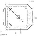
<実施形態1>
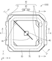
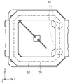
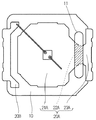
本発明の実施形態1に係る発光装置1000を図1、図2A、図2B、図3A〜図3Cに基づいて説明する。発光装置1000は、発光素子40と、発光素子40が載置される幅広部21Aと、幅広部から延伸し幅広部21Aよりも幅が狭い幅狭部22Aと、幅狭部22Aから延伸し幅狭部22Aよりも幅が広い端子部23Aと、を備える第一リード20Aと、発光素子40と電気的に接続される第二リード20Bと、第一リード20A及び第二リード20Bを支持し、凸部11を備える樹脂部材10と、発光素子40を囲み、凸部11の少なくとも一部を被覆する樹脂枠50と、を有し、樹脂部材10は、幅広部21Aと幅狭部22Aと端子部23Aとに囲まれる位置に凸部11の少なくとも一部を備える。
<
The
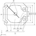
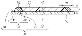
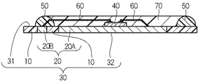
図3Aに示すように、基体30は、第1面31と、第1面31とは反対側の第2面32と、を備えている。図1に示すように、基体30は、導電部材20と、樹脂部材10と、を備えている。導電部材20は、第一リード20Aと、第二リード20Bと、を備えている。樹脂部材10は、第一リード20A及び第二リード20Bを支持している。図2Aに示すように、第一リード20Aは、幅広部21Aと、幅狭部22Aと、端子部23Aと、を備えている。幅広部21Aには、発光素子40が配置される。幅狭部22Aは、発光素子40から離れる方向に幅広部21Aから延伸されてなる。幅狭部22Aの幅W22は、幅広部21Aの幅W21よりも狭い。端子部23Aは、幅狭部22Aから延伸されてなる。端子部23Aの幅W23は、幅狭部22Aの幅W22より広い。幅広部21Aの幅W21と幅狭部22Aの幅W22と端子部23Aの幅W23とは、幅狭部22Aが幅広部21Aから延伸する方向に垂直をなす方向の第一リード20Aの長さとする。図3Bに示すように、樹脂部材10は、第1面31に凸部11を備えている。凸部11の少なくとも一部は、幅広部21Aと幅狭部22Aと端子部23Aとに囲まれる位置に設けられる。図1に示すように、樹脂枠50は、発光素子40を囲み、凸部11の少なくとも一部を被覆している。
As shown in FIG. 3A, the
一般的に、それぞれが樹脂材料を含有する樹脂部材10と樹脂枠50との密着性は、樹脂枠50と樹脂を含有していない導電部材20との密着性よりも高い。これは、樹脂部材10と樹脂枠50が共に樹脂を含有しているので、樹脂部材10と樹脂枠50の熱膨張率を近づけることができるためである。このため、密着性の高い樹脂部材10と樹脂枠50との接触面積を大きくすることで、樹脂枠50と基体30との密着性を効果的に向上させることができる。発光装置1000では、樹脂部材10が凸部11を備えており、凸部11が樹脂枠50に被覆されている。このため、凸部11を備えていない場合よりも樹脂部材10と樹脂枠50との接触面積を大きくすることができる。これにより、樹脂枠50と基体30との密着性を向上させることができる。
In general, the adhesion between the
凸部11は、幅広部21Aと幅狭部22Aと端子部23Aとに囲まれる位置に設けられる。尚、凸部11の全周が、幅広部21Aと幅狭部22Aと端子部23Aとに囲まれていなくてもよい。例えば、図2Aに示すように、凸部11において幅狭部22Aが位置する側と反対側に第一リード20Aが位置しなくてもよい。凸部11が、幅広部21Aと幅狭部22Aと端子部23Aとに囲まれる位置に設けられることで、凸部11が幅広部21Aと端子部23Aとの間に位置する。これにより、基体30の幅W30が広くなりにくい。例えば、幅広部21A及び/又は端子部23Aから、幅狭部22Aが幅広部21Aから延伸する方向に垂直をなす方向に、凸部11を形成する場合と比較して、幅狭部22Aから、幅狭部22Aが幅広部21Aから延伸する方向に垂直をなす方向に、凸部11を形成する方が基体30の幅W30が広くなりにくい。これにより、発光装置を小型化しやすくなる。尚、基体30の幅W30とは幅狭部22Aが幅広部21Aから延伸する方向に垂直をなす方向の基体30の長さとする。
The
凸部11は、幅広部21Aと端子部23Aとから離間する位置に設けられることが好ましい。このようにすることで、樹脂枠50と樹脂部材10との接触面積を大きくすることができるので、樹脂枠50と基体30との密着性を向上させることができる。
The
発光装置1000では、凸部11の形状が円柱である。凸部11の形状が円柱である場合には、成形が容易になる。尚、凸部11の形状は、半球や、円錐や、三角錐、四角錐、五角錐等の角錐や、三角柱、四角柱、五角柱等の角柱等の任意の形状でよい。また、図4Aに示すように、樹脂枠50に覆われる部位の凸部11の表面に凹凸を備えていてもよい。凸部11の表面に凹凸を備えていない場合よりも、凸部11と樹脂枠50との接触面積を大きくすることができる。これにより、樹脂枠50と基体30との密着性を向上させることができる。
In the
図3Bに示すように、凸部11が上面12と側面13とを備える場合には、樹脂枠50が凸部11の上面12及び側面13を被覆していることが好ましい。樹脂枠50が上面12及び側面13を被覆することで、樹脂枠50が凸部11の側面13のみを被覆する場合よりも、樹脂枠50と凸部11との接触面積を大きくすることができるので、樹脂枠50と基体30との密着性を向上させることができる。
As shown in FIG. 3B, when the
図2Bでは、導電部材20における樹脂枠50に被覆されている部位にハッチングをしている。第一リード20Aにおける樹脂枠50に被覆されている部位と、凸部11における樹脂枠50に被覆されている部位との最短距離W11は、1mm以内であることが好ましい。樹脂枠50との密着性が低い導電部材20の近くに、樹脂枠50との密着性が高い凸部11が位置することで、樹脂枠50と基体30との密着性を向上させることができる。
In FIG. 2B, the portion of the
また、第一リード20Aにおける樹脂枠50に被覆されている部位と、凸部11における樹脂枠50に被覆されている部位との最短距離W11が樹脂枠50の幅よりも短いことが好ましい。このようにすることで、樹脂枠50と基体30との密着性を向上させることができる。尚、本明細書で樹脂枠50の幅とは、樹脂枠50の内縁と外縁との最短距離とする。
Further, it is preferable that the shortest distance W11 between the portion of the
凸部11の数は1つでも、複数でもよい。凸部11を複数有する事で凸部11と樹脂枠50との接触面積を大きくすることができるので、樹脂枠50と基体30との密着性を向上させることができる。図2B及び図3Bに示すように、発光装置1000の樹脂部材10は、凸部11を2つ備えている。2つの凸部11の間に第一リード20Aが位置し、一方の凸部11から他方の凸部11に亘って樹脂枠50が配置されている。このようにすることで、樹脂枠50との密着性が低い第一リード20Aの両側に、樹脂枠50との密着性が高い凸部11が位置するので、樹脂枠50と基体30との密着性を向上させることができる。
The number of
凸部11の厚みは、樹脂枠50の厚みの0.4倍以上1倍未満であることが好ましい。凸部11の厚みが、樹脂枠50の厚みの0.4倍以上あることで、凸部11の側面13の面積が大きくなる。これにより、凸部11の側面13と樹脂枠50との接触面積を大きくすることができるので、凸部11と樹脂枠50との密着性を向上させることができる。また、凸部11の厚みが、樹脂枠50の厚みの1倍未満であることで、凸部11の上面12を樹脂枠50で被覆することができる。これにより、凸部11と樹脂枠50との接触面積を大きくすることができるので、凸部11と樹脂枠50との密着性を向上させることができる。尚、凸部11が角錐の場合でも凸部11の厚みが、樹脂枠50の厚みの1倍未満であることで、凸部11の頭頂点を被覆することができるので、凸部11と樹脂枠50との接触面積を大きくすることができる。
The thickness of the
図4Bに示すように、樹脂枠50が凸部11の表面の全てを被覆することが好ましい。このようにすることで、凸部11と樹脂枠50との接触面積を大きくすることができるので、凸部11と樹脂枠50との密着性を向上させることができる。尚、凸部11の厚みとは、z方向の凸部11の最長の長さのことである。
As shown in FIG. 4B, it is preferable that the
発光素子40のピーク波長における樹脂枠50の反射率は、発光素子40のピーク波長における樹脂部材10の反射率よりも高いことが好ましい。このようにすることで、発光素子40からの光を樹脂枠50で反射しやすくなるので、発光装置の光取り出し効率を向上させることができる。
The reflectance of the
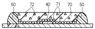
図3Cに示すように、発光素子40と第二リード20Bとは、ワイヤ60によって電気的に接続されている。ワイヤ60と第二リード20Bとの接続部は樹脂枠50によって被覆されることが好ましい。これにより、発光素子40からの光がワイヤ60に吸収されることを抑制できる。
As shown in FIG. 3C, the
図2Bに示すように樹脂枠50は、幅狭部22Aを跨いで配置される。このようにすることで、樹脂枠50が幅広部21A及び/又は端子部23Aを跨いで配置される場合よりも、樹脂枠50と樹脂部材10との接触面積を大きくすることができるので、樹脂枠50と基体30との密着性を向上させることができる。
As shown in FIG. 2B, the
樹脂枠50の内縁と外縁の形状は、上面視で、円形状、楕円形状、正方形、六角形、八角形等の多角形状や、角部を面取りする等様々な形状にしてもよい。特に、図1に示すように樹脂枠50の内縁及び外縁の形状が四角形の角部を面取りした形状が好ましい。樹脂枠50の内縁の角部を面取りすることで、後述する未硬化の封止部材70を樹脂枠50内の角部にも充填させやすくなる。
The shape of the inner edge and the outer edge of the
樹脂枠50の断面は、先端が丸みを帯びた凸形状を有する。内面及び外面が湾曲した樹脂枠50は、硬化前の樹脂枠を内部に保持するシリンジを準備し、シリンジの先端に取り付けた貫通孔を有するニードルから、硬化前の樹脂枠を排出させることで形成できる。
The cross section of the
図3Aに示すように、樹脂枠50の厚みHは、発光素子40の厚みよりも厚い方が好ましい。これにより、樹脂枠50内に形成される封止部材70が発光素子40の上面を覆いやすい。また、樹脂枠50の幅Wは、樹脂枠50の厚みHの0.2倍以上5倍以下が好ましい。樹脂枠50の幅Wが厚みHより0.2倍より薄ければ樹脂枠50の強度が低下する。樹脂枠50の幅Wがz方向の厚みHより5倍より厚ければ、樹脂枠50と発光素子40との距離が近くなり発光素子40からの光の一部が吸収されやすくなる。尚、本明細書で樹脂枠50の厚みHとは、z方向での樹脂枠50の最長の長さとする。発光素子40の厚みとは、z方向での発光素子40の最長の長さとする。
As shown in FIG. 3A, the thickness H of the
樹脂枠50の表面にメッキ層が施されていてもよい。当該メッキ層は、銀、アルミニウム、銅、金等の1又は2以上の金属から構成されていてもよい。当該メッキ層は好ましくは銀から構成され、メッキ層の全てが銀であってもよい。これにより、光取出し効率を向上させることができる。
A plating layer may be applied to the surface of the
封止部材70は、樹脂枠50に囲まれた領域に配置され、発光素子40を封止する。これにより、発光素子40を保護することができる。尚、発光素子40の表面に保護膜を有する場合には、封止部材70は保護膜を介して発光素子40を封止してもよい。
The sealing
封止部材70は、図4Cに示すように中央部が外周部より厚くなるように形成されることが好ましい。中央部が外周部より厚い凸形状にすることにより、封止部材70と空気との界面で発光素子40からの光が反射することが抑制されるので、光取り出し効率を向上させることができる。中央部が外周部より厚い凸形状の封止部材70は、滴下法によって形成することができる。
As shown in FIG. 4C, the sealing
図4Dに示すように封止部材70に波長変換部材71を含有させてもよい。波長変換部材71は、発光素子40が発する第一ピーク波長の光を、この第一ピーク波長とは波長の異なる第二ピーク波長の光に波長変換する部材である。封止部材70に波長変換部材71を含有させることにより、発光素子40が発する第一ピーク波長の光と、波長変換部材71が発する第二ピーク波長の光とが混色された混色光を出力することができる。例えば、発光素子40に青色LEDを、波長変換部材71にYAG等の蛍光体を用いれば、青色LEDの青色光と、この青色光で励起されて蛍光体が発する黄色光とを混合させて得られる白色光を出力する発光装置を構成することができる。
As shown in FIG. 4D, the sealing
波長変換部材71は封止部材70中に均一に分散させてもよいし、封止部材70に偏在させてもよい。封止部材70の上面よりも発光素子40の近傍に波長変換部材71を偏在させてもよい。このようにすることで、水分に弱い波長変換部材71を使用しても封止部材70が保護層としても機能を果たすので波長変換部材71の劣化を抑制できる。水分に弱い波長変換物質としては、KSF系蛍光体等のフッ化物系蛍光体、硫化物系蛍光体、塩化物系蛍光体、ケイ酸塩系蛍光体、リン酸塩系蛍光体等が挙げられる。
The
図4Dに示すように、封止部材70には光拡散材72を含有させてもよい。光拡散材72は、封止部材70との屈折率差により発光素子40からの光を反射及び/又は屈折させて拡散させるものでる。これにより、封止部材70内での輝度ムラを抑制できる。また、封止部材70に波長変換部材71と光拡散材72とが含有されている場合は色ムラを抑制できる。
As shown in FIG. 4D, the sealing
発光装置1000では、発光素子40を1つだけ配置しているが、図4Eに示すように、発光素子40を複数配置してもよい。発光素子40を複数有する場合は、第一リード20Aと第二リード20Bの両方に発光素子40を載置してもよく、複数の発光素子40の全てを第一リード20A上に載置してもよい。第一リード20Aのみに複数の発光素子40を載置することで発光素子40間の距離を狭くすることができ発光装置を小型化できるため好ましい。また、2つの発光素子の一方の発光素子40と他方の発光素子40とを電気的に接続するワイヤ60を形成する場合に、2つの発光素子40間の距離を狭くできるので、ワイヤ60の断線を抑制できる。
In the
図4Eに示すように基体30に保護素子80が載置されていてもよい。保護素子80は、1つでもよいし、複数でもよい。保護素子80は、発光装置に載置される公知のもののいずれでもよい。
As shown in FIG. 4E, the
図4Eに示すように、保護素子80は樹脂枠50内に一部又は全部が被覆されることが好ましい。これにより、発光素子40からの光が保護素子80によって吸収されることを抑制できる。また、発光素子40のピーク波長に対する反射率が保護素子80より高い部材で樹脂枠50を形成することで発光装置の光取り出し効率を向上することができる。
As shown in FIG. 4E, it is preferable that the
<実施形態2>
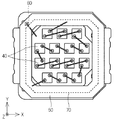
図5A〜図5Cに示す本発明の実施形態2に係る発光装置2000は、実施形態1に係る発光装置1000と比較して、凸部11の形状が相違する。その他の点については、実施形態1と同様である。
<Embodiment 2>
The
図5Bでは、導電部材20における凸部11に被覆されている部位にハッチングをしている。図5B及び図5Cに示すように、凸部11の少なくとも一部が、幅広部21Aと幅狭部22Aと端子部23Aとに囲まれる位置にあり、且つ、幅狭部22Aを被覆している。凸部11が幅狭部22Aを被覆することで、樹脂枠50と樹脂部材10との接触面積を大きくすることができる。これにより、樹脂枠50と基体30との密着性を向上させることができる。
In FIG. 5B, the portion of the
また、凸部11は、幅狭部22Aが幅広部21Aから延伸する方向に垂直をなす方向に延伸して、幅狭部22Aを被覆することが好ましい。このようにすることで、第一リード20Aを被覆する凸部11の面積を小さくすることができる。これにより、樹脂枠50と樹脂部材10との接触面積も大きくすることができるので、樹脂枠50と基体30との密着性を向上させることができる。樹脂部材10の凸部11が、第一リード20Aを跨いで配置されてもよい。このようにすることで、第一リード20Aの上面及び側面を囲むように樹脂部材10が形成されるので、第一リード20Aと樹脂部材10との密着性を向上させることができる。
Further, it is preferable that the
また、凸部11は幅広部21Aと端子部23Aとから離間することが好ましい。幅広部21A及び/又は端子部23Aを被覆する凸部11を形成した場合は、幅広部21A及び/又は端子部23Aの上面に凸部11が位置する。このため、樹脂枠50が、幅広部21A及び/又は端子部23Aを被覆しやすくなる。幅広部21A及び/又は端子部23Aは幅狭部22Aより幅が広いので、樹脂枠50と導電部材20との接触面積が大きくなりやすい。このため、凸部11を幅広部21Aと端子部23Aとから離間させることで、樹脂枠50と樹脂部材10との接触面積を大きくすることができるので、樹脂枠50と基体30との密着性を向上させることができる。
Further, it is preferable that the
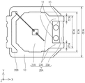
<実施形態3>
図6A、図6Bに示す本発明の実施形態3に係る発光装置3000は、実施形態1に係る発光装置1000と比較して、導電部材20の形状と、凸部11の位置と、が相違する。
<Embodiment 3>
The
図6Bに示すように、凸部11の少なくとも一部は、幅広部21Aと幅狭部22Aと端子部23Aとに囲まれる位置にあり、第一リード20Aは、幅狭部22Aを2箇所有していてもよい。このような場合は、一方の幅狭部22Aと他方の幅狭部22Aとの間に凸部11が位置することが好ましい。このようにすることで、樹脂枠50との密着性が高い凸部11により、樹脂枠50と一方の幅狭部22A及び他方の幅狭部22Aとの密着性を向上させることができる。また、少なくとも一部の樹脂部材10の側面の全周が、一方の幅狭部22A及び他方の幅狭部22Aと、幅広部21Aと、端子部23Aと、に囲まれてもいてもよい。このようにすることで、樹脂部材10の側面の全周が第一リード20Aに囲まれるので、第一リード20Aと樹脂部材10との密着性を向上させることができる。発光装置3000では、凸部11は幅広部21Aと幅狭部22Aと端子部23Aとに囲まれる位置にある。
As shown in FIG. 6B, at least a part of the
以下に、実施形態1〜3の発光装置の各構成部材に適した材料等について説明する。 Hereinafter, materials and the like suitable for each component of the light emitting device of the first to third embodiments will be described.
(基体30)
基体30は、発光素子や保護素子などの電子部品を配置するためのものである。基体30は、樹脂部材10と、導電部材20と、を備える。
(Hypokeimenon 30)
The
(樹脂部材10)
樹脂部材10の材料としては、エポキシ樹脂、シリコーン樹脂、BTレジン、ポリアミド樹脂、ポリイミド樹脂、ナイロン樹脂、不飽和ポリエステル等が挙げられる。これらの樹脂材料に、当該分野で公知の着色剤、充填剤、強化繊維等を含有させてもよい。着色剤として、酸化チタン、酸化亜鉛等の白色のフィラーを用いると発光装置の光取り出し効率を向上させることができる。また、熱放射係数の大きいカーボンブラック等の黒色フィラーを含有させることにより、発光素子からの熱を効率的に逃がすことができる。充填剤としては、酸化ケイ素、酸化アルミニウム等が挙げられる。強化繊維としては、ガラス、珪酸カルシウム、チタン酸カリウム等が挙げられる。
(Resin member 10)
Examples of the material of the
(導電部材20)
導電部材20は、発光素子40等の電子部品に外部電源からの電圧を印加するために用いられる。導電部材20は、第一リード20Aと、第二リード20Bと、を備えている。導電部材20は、z方向に屈曲する部分を有していない板状が好ましい。導電部材20が板状であることにより、基体30の成形が容易になる。
(Conductive member 20)
The
平面視において、第一リード20Aの面積が第二リード20Bの面積より大きい方か好ましい。第一リード20A上には発光素子40が載置されるので第一リード20Aの面積が大きいことで、発光素子40で発生した熱を第一リード20Aに伝導しやすくなる。これにより、発光素子40の温度上昇を抑制できるので発光装置の信頼性を向上できる。
In a plan view, it is preferable that the area of the
導電部材20は樹脂部材10の側面から突出させてもよい。導電部材20の体積が増えることで発光装置の放熱性を向上させることができる。また、発光素子40の直下における第一リード20Aの裏面は樹脂部材10から露出されることが好ましい。発光装置の下面を実装基板に実装した場合に、発光素子40で発生した熱を樹脂部材10から露出された第一リード20Aを介して第一リード20A下の実装基板に伝導しやすくなる。これにより、発光素子40の温度上昇を抑制できるので発光装置の信頼性を向上できる。
The
導電部材20は、熱伝導率の比較的大きな材料で形成することが好ましい。例えば、200W/(m・K)程度以上の熱伝導率を有している材料を用いることにより、発光素子40で発生した熱を第一リード20Aに伝導しやすくなる。
The
導電部材20は、打ち抜き加工や切断加工等が容易な強度の高い材料で形成されることが好ましい。例えば、銅、アルミニウム、金、銀、タングステン、鉄、ニッケル等の金属又はこれらの合金、燐青銅、鉄入り銅等単層又は積層体を基材とすることができる。
The
導電部材20は、表面に反射膜を備えていてもよい。反射膜は、アルミニウム、銅、金等の1又は2以上の金属を用いることができる。特に、反射膜に銀を用いることが好ましい。このようにすることで、発光装置の光取り出し効率を向上させることができる。
The
導電部材20に反射膜を形成する方法は、めっき法、蒸着法、スパッタ法、イオンビームアシスト蒸着法等の種々の方法が挙げられる。その膜厚は、発光素子40からの光を有効に反射させることができる膜厚であればよく、例えば20nm〜10μm程度であり、50nm〜5μm程度が好ましく、100nm〜3μm程度がより好ましい。導電部材の厚み及び形状は、当該分野で公知の範囲において適宜設定することができる。
Examples of the method for forming the reflective film on the
導電部材20として、硫化しやすい銀を用いる場合には導電部材20の表面に保護膜を設けることが好ましい。保護膜を設けることで導電部材20の硫化が抑制され、発光装置の光取り出し効率が低下することを抑制できる。保護膜の材料としては、酸化アルミニウム、酸化ケイ素などの無機材料を用いることができる。
When silver, which is easily sulfurized, is used as the
図3Aに示すように、第一リード20A及び/又は第二リード20Bの端面は凹凸を備えることが好ましい。第一リード20A及び/又は第二リード20Bと、樹脂部材10と、が接触する箇所に凹凸を備えることで、第一リード20A及び/又は第二リード20Bと、樹脂部材10と、の接触面積を大きくすることができる。これにより、第一リード20A及び/又は第二リード20Bと樹脂部材10との密着性を向上させることができる。
As shown in FIG. 3A, the end faces of the
(発光素子40)
発光素子40は、第一リード20Aの第1面31上に配置される。発光素子40は、電圧を印加することで自ら発光する半導体素子であり、窒化物半導体等から構成される既知の半導体素子を適用できる。発光素子の発光波長は、可視域(380〜780nm)を含め、紫外域から赤外域まで選択することができる。例えば、ピーク波長430〜490nmの発光素子としては、窒化物半導体を用いることができる。その窒化物半導体としては、InXAlYGa1−X−YN(0≦X、0≦Y、X+Y≦1)等を用いることができる。また、発光素子40はサブマウントを介して第1面31上に配置されてもよい。
(Light emitting element 40)
The
発光素子40の形状は、上面視で、三角形、四角形、六角形等の多角形、又はこれらに近似する形状等、任意の形状でよい。また、発光素子40は、同じ面側にn電極及びp電極が形成された片面電極のものであってもよいし、n電極とp電極が互いに反対側となる2つの面(例えば上面と下面)に各々形成された両面電極のものであってもよい。
The shape of the
発光素子40が片面電極の場合は、第一リード20Aの第1面31上にフェイスアップ実装される。フェイスアップ実装とは、発光素子40の電極形成面と反対側の面を基体30に向けて実装する形態である。発光素子40と第一リード20Aの接合部材は、絶縁性の接合部材でも導電性の接合部材でもよく、公知の接合部材を用いてよい。例えば、絶縁性の接合部材としてはエポキシ樹脂、シリコーン樹脂又はこれらの変性樹脂等が挙げられ、導電性の接合部材としては銀、金、パラジウム等の導電性ペーストや、Au−Sn共晶等の半田、低融点金属等のろう材等が挙げられる。
When the
発光素子40が両面電極の場合は、発光素子40と第一リード20Aとの接合部材として、導電性の接合部材であればよく公知の接合部材を用いてよい。例えば、導電性の接合部材としては銀、金、パラジウム等の導電性ペーストや、Au−Sn共晶等の半田、低融点金属等のろう材等が挙げられる。この場合、発光素子を第一リード20Aに載置することで、発光素子40と、第一リード20Aと、を電気的に接続することができる。
When the
(樹脂枠50)
樹脂枠50は、環状に発光素子40を囲んで設けられる。樹脂枠50が発光素子40を囲んで設けられるため、封止部材70となる未硬化状態の原料を樹脂枠50内に止めることができる。樹脂枠50は、樹脂枠50の元となる未硬化の原料を、樹脂枠50を形成したい領域に配置し、当該原料を硬化させることにより形成される。
(Resin frame 50)
The
樹脂枠50の材料としては、フェノール樹脂、エポキシ樹脂、BTレジンやPPAやシリコーン樹脂などが挙げられる。特に、樹脂枠50の材料としては、耐光性に優れたシリコーン樹脂が好ましい。また、これらの母体となる樹脂に、発光素子40からの光を吸収しにくく、かつ、母体となる樹脂に対する屈折率差の大きい反射部材等の粉末を分散することで、効率よく発光素子40からの光を反射させることができる。反射部材としては、例えば、酸化チタン、酸化アルミニウム、酸化ジルコニウム、酸化マグネシウムを用いることができる。特に、酸化チタンは、水分などに対して比較的安定でかつ高屈折率であるため好ましい。樹脂枠50は、発光素子40からの光に対する反射率が60%以上、好ましくは70%以上の部材である。このようにすることで、樹脂枠50に達した光が樹脂枠50に吸収されにくくなり、発光装置の光取出し効率を高めることができる。
Examples of the material of the
(ワイヤ60)
発光素子40と第二リード20Bとは、ワイヤ60を介して電気的に接続してもよい。ワイヤ60は、導電性に優れた金属材料を用いることができる。金属材料としては、金やアルミニウム、銅、銀等を用いることができる。ワイヤボンディングの方法としては、ボールボンディング、ウェッジボンディング等の公知の方法を用いてよい。
(Wire 60)
The
(封止部材70)
封止部材70の材料としては、透光性を有する樹脂材料又はガラス材料等を用いることができる。特に、封止部材70の材料に樹脂材料を用いることが好ましい。樹脂部材10及び樹脂枠50がそれぞれ樹脂材料を含有しているので、封止部材70も樹脂材料であることで、封止部材70と樹脂部材10との密着性、及び、封止部材70と樹脂枠50との密着性を向上させることができる。封止部材70の樹脂材料としては、ポリカーボネート樹脂、エポキシ樹脂、フェノール樹脂、シリコーン樹脂、アクリル樹脂、ポリメチルペンテン樹脂、ポリノルボルネン樹脂、又はこれらの変性樹脂やこれらの樹脂を1種以上含むハイブリッド樹脂等を用いることができる。特に、封止部材70の材料としては耐光性に優れたジメチル系シリコーン樹脂、フェニル系シリコーン樹脂が好ましい。
(Sealing member 70)
As the material of the sealing
(波長変換部材71)
波長変換部材71としては、発光素子からの発光で励起可能な蛍光体の粒子が使用される。例えば、青色発光素子又は紫外線発光素子で励起可能な蛍光体としては、セリウムで賦活されたイットリウム・アルミニウム・ガーネット系蛍光体(YAG:Ce)、セリウムで賦活されたルテチウム・アルミニウム・ガーネット系蛍光体(LAG:Ce)、ユウロピウムおよび/又はクロムで賦活された窒素含有アルミノ珪酸カルシウム系蛍光体(CaO−Al2O3−SiO2:Eu,Cr)、ユウロピウムで賦活されたシリケート系蛍光体((Sr,Ba)2SiO4:Eu)、βサイアロン蛍光体、CASN系蛍光体、SCASN系蛍光体等の室化物系蛍光体;KSF系蛍光体等のフッ化物系蛍光体、硫化物系蛍光体、塩化物系蛍光体、ケイ酸塩系蛍光体、リン酸塩系蛍光体、量子ドット蛍光体などが挙げられる。これらの蛍光体と、青色発光素子又は紫外線発光素子と組み合わせることにより、様々な波長の発光装置を製造することができる。
(Wavelength conversion member 71)
As the
(光拡散材72)
光拡散材72の材料として、酸化チタン、酸化ジルコニウム、酸化アルミニウム、酸化ケイ素などを用いることができる。特に、酸化チタンは、水分などに対して比較的安定でかつ高屈折率であるため好ましい。
(Light diffuser 72)
As the material of the
(保護素子80)
保護素子80は、例えば、発光素子40に逆方向に電圧が印加されたときに、逆方向に流れる電流を阻止したり、発光素子40の動作電圧より高い順方向電圧が印加されたときに発光素子に過電流が流れるのを阻止したりすることができる保護回路や静電保護素子が挙げられる。具体的には、ツェナーダイオードが利用できる。
(Protective element 80)
For example, the
以上、本発明に係るいくつかの実施形態について例示したが、本発明は上述した実施形態に限定されるものではなく、本発明の要旨を逸脱しない限り任意のものとすることができることは言うまでもない。 Although some embodiments of the present invention have been illustrated above, it goes without saying that the present invention is not limited to the above-described embodiments and can be arbitrary as long as it does not deviate from the gist of the present invention. ..
1000、2000 発光装置
10 樹脂部材
11 凸部
20 導電部材
20A 第一リード
20B 第二リード
30 基体
31 第1面
32 第2面
40 発光素子
50 樹脂枠
60 ワイヤ
70 封止部材
71 波長変換部材
72 光拡散材
80 保護素子
1000, 2000
Claims (17)
前記発光素子が載置される幅広部と、前記幅広部から延伸し前記幅広部よりも幅が狭い幅狭部と、前記幅狭部から延伸し前記幅狭部よりも幅が広い端子部と、を備える第一リードと、
前記発光素子と電気的に接続される第二リードと、
前記第一リード及び第二リードを支持し、凸部を備える樹脂部材と、
前記発光素子を囲み、前記凸部の少なくとも一部を被覆する樹脂枠と、を有し、
前記凸部は、それぞれ前記幅広部と前記幅狭部と前記端子部とに囲まれる位置に設けられた第1凸部と第2凸部からなり、
前記第一リードは前記第1凸部と前記第2凸部の間に位置する発光装置。 Light emitting element and
A wide portion on which the light emitting element is placed, a narrow portion extending from the wide portion and narrower than the wide portion, and a terminal portion extending from the narrow portion and wider than the narrow portion. With the first lead,
A second lead that is electrically connected to the light emitting element,
A resin member that supports the first lead and the second lead and has a convex portion,
It has a resin frame that surrounds the light emitting element and covers at least a part of the convex portion.
The convex portion is Ri Do from the first protrusion and a second protrusion provided at a position surrounded by a respective said wide portion and the narrow portion and the terminal portion,
Wherein the first lead you located between said first protrusions second protrusion emitting device.
前記発光素子が載置される幅広部と、前記幅広部から延伸し前記幅広部よりも幅が狭い幅狭部と、前記幅狭部から延伸し前記幅狭部よりも幅が広い端子部と、を備える第一リードと、
前記発光素子と電気的に接続される第二リードと、
前記第一リード及び第二リードを支持し、凸部を備える樹脂部材と、
前記発光素子を囲み、前記凸部の少なくとも一部を被覆する樹脂枠と、を有し、
前記凸部は円柱形状であり、前記幅広部と前記幅狭部と前記端子部とに囲まれる位置に設けられた発光装置。 Light emitting element and
A wide portion on which the light emitting element is placed, a narrow portion extending from the wide portion and narrower than the wide portion, and a terminal portion extending from the narrow portion and wider than the narrow portion. With the first lead,
A second lead that is electrically connected to the light emitting element,
A resin member that supports the first lead and the second lead and has a convex portion,
It has a resin frame that surrounds the light emitting element and covers at least a part of the convex portion.
The convex portion has a cylindrical shape, and is a light emitting device provided at a position surrounded by the wide portion, the narrow portion, and the terminal portion.
前記第1凸部から前記第2凸部に亘って前記樹脂枠が配置されている請求項1、2及び4〜6のいずれか1項に記載の発光装置。 The first lead is located between the first convex portion and the second convex portion.
The light emitting device according to any one of claims 1, 2 and 4 to 6, wherein the resin frame is arranged from the first convex portion to the second convex portion.
Priority Applications (4)
| Application Number | Priority Date | Filing Date | Title |
|---|---|---|---|
| JP2016070432A JP6790416B2 (en) | 2016-03-31 | 2016-03-31 | Light emitting device |
| US15/473,505 US10593847B2 (en) | 2016-03-31 | 2017-03-29 | Light emitting device |
| CN201710204609.4A CN107275301B (en) | 2016-03-31 | 2017-03-30 | Light emitting device |
| EP17163854.7A EP3226312B1 (en) | 2016-03-31 | 2017-03-30 | Light emitting device |
Applications Claiming Priority (1)
| Application Number | Priority Date | Filing Date | Title |
|---|---|---|---|
| JP2016070432A JP6790416B2 (en) | 2016-03-31 | 2016-03-31 | Light emitting device |
Publications (3)
| Publication Number | Publication Date |
|---|---|
| JP2017183578A JP2017183578A (en) | 2017-10-05 |
| JP2017183578A5 JP2017183578A5 (en) | 2018-10-18 |
| JP6790416B2 true JP6790416B2 (en) | 2020-11-25 |
Family
ID=58464303
Family Applications (1)
| Application Number | Title | Priority Date | Filing Date |
|---|---|---|---|
| JP2016070432A Active JP6790416B2 (en) | 2016-03-31 | 2016-03-31 | Light emitting device |
Country Status (4)
| Country | Link |
|---|---|
| US (1) | US10593847B2 (en) |
| EP (1) | EP3226312B1 (en) |
| JP (1) | JP6790416B2 (en) |
| CN (1) | CN107275301B (en) |
Families Citing this family (17)
| Publication number | Priority date | Publication date | Assignee | Title |
|---|---|---|---|---|
| JP6777105B2 (en) | 2018-01-31 | 2020-10-28 | 日亜化学工業株式会社 | Manufacturing method of light emitting device |
| JP7037046B2 (en) * | 2018-01-31 | 2022-03-16 | 日亜化学工業株式会社 | Light emitting device and its manufacturing method |
| JP6777104B2 (en) * | 2018-01-31 | 2020-10-28 | 日亜化学工業株式会社 | Light emitting device and its manufacturing method |
| JP6822442B2 (en) * | 2018-03-01 | 2021-01-27 | 日亜化学工業株式会社 | Light emitting device and its manufacturing method |
| US10873015B2 (en) | 2018-03-01 | 2020-12-22 | Nichia Corporation | Light emitting device and method of manufacturing the light emitting device |
| JP6760324B2 (en) | 2018-03-27 | 2020-09-23 | 日亜化学工業株式会社 | Light emitting device |
| JP6879270B2 (en) * | 2018-07-20 | 2021-06-02 | 日亜化学工業株式会社 | Light emitting device |
| JP6975916B2 (en) * | 2018-08-09 | 2021-12-01 | 日亜化学工業株式会社 | Luminescent device |
| KR102646700B1 (en) * | 2018-08-16 | 2024-03-13 | 엘지이노텍 주식회사 | Lighting apparatus |
| JP7181489B2 (en) * | 2019-01-31 | 2022-12-01 | 日亜化学工業株式会社 | Light emitting device and manufacturing method thereof |
| JP7248887B2 (en) * | 2019-02-15 | 2023-03-30 | 日亜化学工業株式会社 | Resin package and light emitting device |
| JP6916450B2 (en) * | 2019-04-01 | 2021-08-11 | 日亜化学工業株式会社 | Light emitting device and its manufacturing method |
| JP7121312B2 (en) * | 2020-03-26 | 2022-08-18 | 日亜化学工業株式会社 | light emitting device |
| US11769862B2 (en) | 2020-03-26 | 2023-09-26 | Nichia Corporation | Light emitting device |
| JP7137084B2 (en) * | 2020-09-02 | 2022-09-14 | 日亜化学工業株式会社 | light emitting device |
| JP7389363B2 (en) * | 2021-05-26 | 2023-11-30 | 日亜化学工業株式会社 | light emitting device |
| JP2023082632A (en) * | 2021-12-02 | 2023-06-14 | スタンレー電気株式会社 | semiconductor light emitting device |
Family Cites Families (30)
| Publication number | Priority date | Publication date | Assignee | Title |
|---|---|---|---|---|
| JP4307090B2 (en) * | 2003-01-27 | 2009-08-05 | 京セラ株式会社 | Light emitting element storage package and light emitting device |
| DE112006004259A5 (en) * | 2005-11-21 | 2012-09-06 | Seoul Semiconductor Co., Ltd. | Light-emitting element |
| JP2008108836A (en) * | 2006-10-24 | 2008-05-08 | Sharp Corp | Semiconductor light emitting device and manufacturing method thereof |
| JP5236406B2 (en) | 2008-03-28 | 2013-07-17 | ローム株式会社 | Semiconductor light emitting module and manufacturing method thereof |
| KR100888236B1 (en) | 2008-11-18 | 2009-03-12 | 서울반도체 주식회사 | Light emitting device |
| JP2011100862A (en) * | 2009-11-06 | 2011-05-19 | Sanyo Electric Co Ltd | Light-emitting device and method of manufacturing the same |
| TW201128812A (en) | 2009-12-01 | 2011-08-16 | Lg Innotek Co Ltd | Light emitting device |
| KR101064084B1 (en) * | 2010-03-25 | 2011-09-08 | 엘지이노텍 주식회사 | Light emitting device package and manufacturing method thereof |
| KR101039994B1 (en) * | 2010-05-24 | 2011-06-09 | 엘지이노텍 주식회사 | Light emitting device and light unit having same |
| JP5481277B2 (en) | 2010-06-04 | 2014-04-23 | シャープ株式会社 | Light emitting device |
| CN103392242B (en) * | 2011-02-28 | 2017-02-22 | 日亚化学工业株式会社 | Light emitting device |
| KR101832306B1 (en) * | 2011-05-30 | 2018-02-26 | 엘지이노텍 주식회사 | Light emitting device pakage |
| JP2012256651A (en) | 2011-06-07 | 2012-12-27 | Mitsubishi Chemicals Corp | Resin package for semiconductor light-emitting device and manufacturing method therefor and semiconductor light-emitting device having resin package |
| KR101830717B1 (en) * | 2011-06-30 | 2018-02-21 | 엘지이노텍 주식회사 | A light emitting device pakage |
| JP2013041950A (en) * | 2011-08-12 | 2013-02-28 | Sharp Corp | Light emitting device |
| JP2013058739A (en) * | 2011-08-17 | 2013-03-28 | Dainippon Printing Co Ltd | Optical semiconductor device lead frame, optical semiconductor device lead frame with resin, optical semiconductor device, and optical semiconductor device lead frame manufacturing method |
| KR101905535B1 (en) * | 2011-11-16 | 2018-10-10 | 엘지이노텍 주식회사 | Light emitting device and light apparatus having thereof |
| ES2693677T3 (en) * | 2011-11-17 | 2018-12-13 | Lumens Co., Ltd. | Package of a light emitting and backlighting device that includes the same |
| JP2013206895A (en) | 2012-03-27 | 2013-10-07 | Shin Etsu Chem Co Ltd | Substrate for optical semiconductor device, manufacturing method of substrate for optical semiconductor device, optical semiconductor device, and manufacturing method of optical semiconductor device |
| KR101911047B1 (en) * | 2012-07-25 | 2018-10-24 | 삼성디스플레이 주식회사 | Case and display device |
| US20140070235A1 (en) | 2012-09-07 | 2014-03-13 | Peter Scott Andrews | Wire bonds and light emitter devices and related methods |
| KR102019499B1 (en) | 2012-11-05 | 2019-09-06 | 엘지이노텍 주식회사 | Light emitting device and lighting systme having thereof |
| JP2014120515A (en) * | 2012-12-13 | 2014-06-30 | Shin Etsu Chem Co Ltd | Substrate for optical semiconductor device and method of manufacturing the same, aggregate substrate, and optical semiconductor device and method of manufacturing the same |
| KR102029802B1 (en) * | 2013-01-14 | 2019-10-08 | 엘지이노텍 주식회사 | Light emitting device and light apparatus having thereof |
| JP6476567B2 (en) | 2013-03-29 | 2019-03-06 | 日亜化学工業株式会社 | Light emitting device |
| JP6303457B2 (en) | 2013-12-04 | 2018-04-04 | 日亜化学工業株式会社 | Light emitting device and manufacturing method thereof |
| JP2015115407A (en) * | 2013-12-10 | 2015-06-22 | 三星電子株式会社Samsung Electronics Co.,Ltd. | Light-emitting element wiring board, semiconductor light-emitting device, and method for manufacturing the same |
| JP6487626B2 (en) * | 2014-03-24 | 2019-03-20 | スタンレー電気株式会社 | Semiconductor device |
| JP6274434B2 (en) * | 2014-07-30 | 2018-02-07 | 豊田合成株式会社 | Silicone resin composition and light emitting device using the same |
| JP2016070432A (en) | 2014-09-30 | 2016-05-09 | アイシン・エィ・ダブリュ株式会社 | Friction engagement device and drive transmission device |
-
2016
- 2016-03-31 JP JP2016070432A patent/JP6790416B2/en active Active
-
2017
- 2017-03-29 US US15/473,505 patent/US10593847B2/en active Active
- 2017-03-30 CN CN201710204609.4A patent/CN107275301B/en active Active
- 2017-03-30 EP EP17163854.7A patent/EP3226312B1/en active Active
Also Published As
| Publication number | Publication date |
|---|---|
| US10593847B2 (en) | 2020-03-17 |
| US20170288104A1 (en) | 2017-10-05 |
| JP2017183578A (en) | 2017-10-05 |
| CN107275301A (en) | 2017-10-20 |
| EP3226312A1 (en) | 2017-10-04 |
| CN107275301B (en) | 2022-08-02 |
| EP3226312B1 (en) | 2021-03-24 |
Similar Documents
| Publication | Publication Date | Title |
|---|---|---|
| JP6790416B2 (en) | Light emitting device | |
| JP6387954B2 (en) | Method for manufacturing light emitting device using wavelength conversion member | |
| JP6925100B2 (en) | Light emitting device | |
| US11233184B2 (en) | Light-emitting device and method for manufacturing the same | |
| US20130126927A1 (en) | Semiconductor light emitting device | |
| JP6587499B2 (en) | Light emitting device and manufacturing method thereof | |
| JP6606966B2 (en) | Light emitting device and manufacturing method thereof | |
| CN107026228B (en) | light-emitting device | |
| JP6225910B2 (en) | Light emitting device | |
| JP6760324B2 (en) | Light emitting device | |
| JP6326830B2 (en) | Light emitting device and lighting device including the same | |
| JP6658787B2 (en) | Light emitting device | |
| JP7137079B2 (en) | Light emitting device and manufacturing method thereof | |
| JP6575065B2 (en) | Light emitting device | |
| JP6974746B2 (en) | Light emitting device and its manufacturing method | |
| JP2019041094A (en) | Light-emitting device | |
| JP2018191015A (en) | Method for manufacturing light emitting device | |
| JP7181489B2 (en) | Light emitting device and manufacturing method thereof | |
| JP7137084B2 (en) | light emitting device | |
| JP6593062B2 (en) | Light emitting device | |
| JP7121312B2 (en) | light emitting device | |
| JP7177327B2 (en) | light emitting device |
Legal Events
| Date | Code | Title | Description |
|---|---|---|---|
| RD03 | Notification of appointment of power of attorney |
Free format text: JAPANESE INTERMEDIATE CODE: A7423 Effective date: 20170202 |
|
| A521 | Request for written amendment filed |
Free format text: JAPANESE INTERMEDIATE CODE: A523 Effective date: 20180907 |
|
| A621 | Written request for application examination |
Free format text: JAPANESE INTERMEDIATE CODE: A621 Effective date: 20180907 |
|
| A977 | Report on retrieval |
Free format text: JAPANESE INTERMEDIATE CODE: A971007 Effective date: 20190712 |
|
| A131 | Notification of reasons for refusal |
Free format text: JAPANESE INTERMEDIATE CODE: A131 Effective date: 20190730 |
|
| A521 | Request for written amendment filed |
Free format text: JAPANESE INTERMEDIATE CODE: A523 Effective date: 20190926 |
|
| A131 | Notification of reasons for refusal |
Free format text: JAPANESE INTERMEDIATE CODE: A131 Effective date: 20200303 |
|
| A521 | Request for written amendment filed |
Free format text: JAPANESE INTERMEDIATE CODE: A523 Effective date: 20200410 |
|
| TRDD | Decision of grant or rejection written | ||
| A01 | Written decision to grant a patent or to grant a registration (utility model) |
Free format text: JAPANESE INTERMEDIATE CODE: A01 Effective date: 20201006 |
|
| A61 | First payment of annual fees (during grant procedure) |
Free format text: JAPANESE INTERMEDIATE CODE: A61 Effective date: 20201019 |
|
| R150 | Certificate of patent or registration of utility model |
Ref document number: 6790416 Country of ref document: JP Free format text: JAPANESE INTERMEDIATE CODE: R150 |
|
| R250 | Receipt of annual fees |
Free format text: JAPANESE INTERMEDIATE CODE: R250 |
|
| R250 | Receipt of annual fees |
Free format text: JAPANESE INTERMEDIATE CODE: R250 |
|
| R250 | Receipt of annual fees |
Free format text: JAPANESE INTERMEDIATE CODE: R250 |