CN107275301B - Light emitting device - Google Patents
Light emitting device Download PDFInfo
- Publication number
- CN107275301B CN107275301B CN201710204609.4A CN201710204609A CN107275301B CN 107275301 B CN107275301 B CN 107275301B CN 201710204609 A CN201710204609 A CN 201710204609A CN 107275301 B CN107275301 B CN 107275301B
- Authority
- CN
- China
- Prior art keywords
- light
- lead
- resin
- resin frame
- emitting element
- Prior art date
- Legal status (The legal status is an assumption and is not a legal conclusion. Google has not performed a legal analysis and makes no representation as to the accuracy of the status listed.)
- Active
Links
Images


Classifications
-
- H—ELECTRICITY
- H01—ELECTRIC ELEMENTS
- H01L—SEMICONDUCTOR DEVICES NOT COVERED BY CLASS H10
- H01L33/00—Semiconductor devices with at least one potential-jump barrier or surface barrier specially adapted for light emission; Processes or apparatus specially adapted for the manufacture or treatment thereof or of parts thereof; Details thereof
- H01L33/48—Semiconductor devices with at least one potential-jump barrier or surface barrier specially adapted for light emission; Processes or apparatus specially adapted for the manufacture or treatment thereof or of parts thereof; Details thereof characterised by the semiconductor body packages
- H01L33/62—Arrangements for conducting electric current to or from the semiconductor body, e.g. lead-frames, wire-bonds or solder balls
-
- H—ELECTRICITY
- H01—ELECTRIC ELEMENTS
- H01L—SEMICONDUCTOR DEVICES NOT COVERED BY CLASS H10
- H01L25/00—Assemblies consisting of a plurality of individual semiconductor or other solid state devices ; Multistep manufacturing processes thereof
- H01L25/03—Assemblies consisting of a plurality of individual semiconductor or other solid state devices ; Multistep manufacturing processes thereof all the devices being of a type provided for in the same subgroup of groups H01L27/00 - H01L33/00, or in a single subclass of H10K, H10N, e.g. assemblies of rectifier diodes
- H01L25/04—Assemblies consisting of a plurality of individual semiconductor or other solid state devices ; Multistep manufacturing processes thereof all the devices being of a type provided for in the same subgroup of groups H01L27/00 - H01L33/00, or in a single subclass of H10K, H10N, e.g. assemblies of rectifier diodes the devices not having separate containers
- H01L25/075—Assemblies consisting of a plurality of individual semiconductor or other solid state devices ; Multistep manufacturing processes thereof all the devices being of a type provided for in the same subgroup of groups H01L27/00 - H01L33/00, or in a single subclass of H10K, H10N, e.g. assemblies of rectifier diodes the devices not having separate containers the devices being of a type provided for in group H01L33/00
- H01L25/0753—Assemblies consisting of a plurality of individual semiconductor or other solid state devices ; Multistep manufacturing processes thereof all the devices being of a type provided for in the same subgroup of groups H01L27/00 - H01L33/00, or in a single subclass of H10K, H10N, e.g. assemblies of rectifier diodes the devices not having separate containers the devices being of a type provided for in group H01L33/00 the devices being arranged next to each other
-
- H—ELECTRICITY
- H01—ELECTRIC ELEMENTS
- H01L—SEMICONDUCTOR DEVICES NOT COVERED BY CLASS H10
- H01L23/00—Details of semiconductor or other solid state devices
- H01L23/48—Arrangements for conducting electric current to or from the solid state body in operation, e.g. leads, terminal arrangements ; Selection of materials therefor
- H01L23/481—Internal lead connections, e.g. via connections, feedthrough structures
-
- H—ELECTRICITY
- H01—ELECTRIC ELEMENTS
- H01L—SEMICONDUCTOR DEVICES NOT COVERED BY CLASS H10
- H01L27/00—Devices consisting of a plurality of semiconductor or other solid-state components formed in or on a common substrate
- H01L27/15—Devices consisting of a plurality of semiconductor or other solid-state components formed in or on a common substrate including semiconductor components with at least one potential-jump barrier or surface barrier specially adapted for light emission
- H01L27/153—Devices consisting of a plurality of semiconductor or other solid-state components formed in or on a common substrate including semiconductor components with at least one potential-jump barrier or surface barrier specially adapted for light emission in a repetitive configuration, e.g. LED bars
- H01L27/156—Devices consisting of a plurality of semiconductor or other solid-state components formed in or on a common substrate including semiconductor components with at least one potential-jump barrier or surface barrier specially adapted for light emission in a repetitive configuration, e.g. LED bars two-dimensional arrays
-
- H—ELECTRICITY
- H01—ELECTRIC ELEMENTS
- H01L—SEMICONDUCTOR DEVICES NOT COVERED BY CLASS H10
- H01L33/00—Semiconductor devices with at least one potential-jump barrier or surface barrier specially adapted for light emission; Processes or apparatus specially adapted for the manufacture or treatment thereof or of parts thereof; Details thereof
- H01L33/48—Semiconductor devices with at least one potential-jump barrier or surface barrier specially adapted for light emission; Processes or apparatus specially adapted for the manufacture or treatment thereof or of parts thereof; Details thereof characterised by the semiconductor body packages
- H01L33/483—Containers
- H01L33/486—Containers adapted for surface mounting
-
- H—ELECTRICITY
- H01—ELECTRIC ELEMENTS
- H01L—SEMICONDUCTOR DEVICES NOT COVERED BY CLASS H10
- H01L33/00—Semiconductor devices with at least one potential-jump barrier or surface barrier specially adapted for light emission; Processes or apparatus specially adapted for the manufacture or treatment thereof or of parts thereof; Details thereof
- H01L33/48—Semiconductor devices with at least one potential-jump barrier or surface barrier specially adapted for light emission; Processes or apparatus specially adapted for the manufacture or treatment thereof or of parts thereof; Details thereof characterised by the semiconductor body packages
- H01L33/52—Encapsulations
- H01L33/54—Encapsulations having a particular shape
-
- H—ELECTRICITY
- H01—ELECTRIC ELEMENTS
- H01L—SEMICONDUCTOR DEVICES NOT COVERED BY CLASS H10
- H01L33/00—Semiconductor devices with at least one potential-jump barrier or surface barrier specially adapted for light emission; Processes or apparatus specially adapted for the manufacture or treatment thereof or of parts thereof; Details thereof
- H01L33/48—Semiconductor devices with at least one potential-jump barrier or surface barrier specially adapted for light emission; Processes or apparatus specially adapted for the manufacture or treatment thereof or of parts thereof; Details thereof characterised by the semiconductor body packages
- H01L33/52—Encapsulations
- H01L33/56—Materials, e.g. epoxy or silicone resin
-
- H—ELECTRICITY
- H01—ELECTRIC ELEMENTS
- H01L—SEMICONDUCTOR DEVICES NOT COVERED BY CLASS H10
- H01L33/00—Semiconductor devices with at least one potential-jump barrier or surface barrier specially adapted for light emission; Processes or apparatus specially adapted for the manufacture or treatment thereof or of parts thereof; Details thereof
- H01L33/48—Semiconductor devices with at least one potential-jump barrier or surface barrier specially adapted for light emission; Processes or apparatus specially adapted for the manufacture or treatment thereof or of parts thereof; Details thereof characterised by the semiconductor body packages
- H01L33/58—Optical field-shaping elements
- H01L33/60—Reflective elements
-
- H—ELECTRICITY
- H01—ELECTRIC ELEMENTS
- H01L—SEMICONDUCTOR DEVICES NOT COVERED BY CLASS H10
- H01L2224/00—Indexing scheme for arrangements for connecting or disconnecting semiconductor or solid-state bodies and methods related thereto as covered by H01L24/00
- H01L2224/01—Means for bonding being attached to, or being formed on, the surface to be connected, e.g. chip-to-package, die-attach, "first-level" interconnects; Manufacturing methods related thereto
- H01L2224/42—Wire connectors; Manufacturing methods related thereto
- H01L2224/47—Structure, shape, material or disposition of the wire connectors after the connecting process
- H01L2224/48—Structure, shape, material or disposition of the wire connectors after the connecting process of an individual wire connector
- H01L2224/4805—Shape
- H01L2224/4809—Loop shape
- H01L2224/48091—Arched
-
- H—ELECTRICITY
- H01—ELECTRIC ELEMENTS
- H01L—SEMICONDUCTOR DEVICES NOT COVERED BY CLASS H10
- H01L2224/00—Indexing scheme for arrangements for connecting or disconnecting semiconductor or solid-state bodies and methods related thereto as covered by H01L24/00
- H01L2224/01—Means for bonding being attached to, or being formed on, the surface to be connected, e.g. chip-to-package, die-attach, "first-level" interconnects; Manufacturing methods related thereto
- H01L2224/42—Wire connectors; Manufacturing methods related thereto
- H01L2224/47—Structure, shape, material or disposition of the wire connectors after the connecting process
- H01L2224/48—Structure, shape, material or disposition of the wire connectors after the connecting process of an individual wire connector
- H01L2224/4805—Shape
- H01L2224/4809—Loop shape
- H01L2224/48095—Kinked
-
- H—ELECTRICITY
- H01—ELECTRIC ELEMENTS
- H01L—SEMICONDUCTOR DEVICES NOT COVERED BY CLASS H10
- H01L2224/00—Indexing scheme for arrangements for connecting or disconnecting semiconductor or solid-state bodies and methods related thereto as covered by H01L24/00
- H01L2224/01—Means for bonding being attached to, or being formed on, the surface to be connected, e.g. chip-to-package, die-attach, "first-level" interconnects; Manufacturing methods related thereto
- H01L2224/42—Wire connectors; Manufacturing methods related thereto
- H01L2224/47—Structure, shape, material or disposition of the wire connectors after the connecting process
- H01L2224/48—Structure, shape, material or disposition of the wire connectors after the connecting process of an individual wire connector
- H01L2224/481—Disposition
- H01L2224/48151—Connecting between a semiconductor or solid-state body and an item not being a semiconductor or solid-state body, e.g. chip-to-substrate, chip-to-passive
- H01L2224/48221—Connecting between a semiconductor or solid-state body and an item not being a semiconductor or solid-state body, e.g. chip-to-substrate, chip-to-passive the body and the item being stacked
- H01L2224/48245—Connecting between a semiconductor or solid-state body and an item not being a semiconductor or solid-state body, e.g. chip-to-substrate, chip-to-passive the body and the item being stacked the item being metallic
- H01L2224/48247—Connecting between a semiconductor or solid-state body and an item not being a semiconductor or solid-state body, e.g. chip-to-substrate, chip-to-passive the body and the item being stacked the item being metallic connecting the wire to a bond pad of the item
-
- H—ELECTRICITY
- H01—ELECTRIC ELEMENTS
- H01L—SEMICONDUCTOR DEVICES NOT COVERED BY CLASS H10
- H01L2224/00—Indexing scheme for arrangements for connecting or disconnecting semiconductor or solid-state bodies and methods related thereto as covered by H01L24/00
- H01L2224/01—Means for bonding being attached to, or being formed on, the surface to be connected, e.g. chip-to-package, die-attach, "first-level" interconnects; Manufacturing methods related thereto
- H01L2224/42—Wire connectors; Manufacturing methods related thereto
- H01L2224/47—Structure, shape, material or disposition of the wire connectors after the connecting process
- H01L2224/48—Structure, shape, material or disposition of the wire connectors after the connecting process of an individual wire connector
- H01L2224/481—Disposition
- H01L2224/48151—Connecting between a semiconductor or solid-state body and an item not being a semiconductor or solid-state body, e.g. chip-to-substrate, chip-to-passive
- H01L2224/48221—Connecting between a semiconductor or solid-state body and an item not being a semiconductor or solid-state body, e.g. chip-to-substrate, chip-to-passive the body and the item being stacked
- H01L2224/48245—Connecting between a semiconductor or solid-state body and an item not being a semiconductor or solid-state body, e.g. chip-to-substrate, chip-to-passive the body and the item being stacked the item being metallic
- H01L2224/48257—Connecting between a semiconductor or solid-state body and an item not being a semiconductor or solid-state body, e.g. chip-to-substrate, chip-to-passive the body and the item being stacked the item being metallic connecting the wire to a die pad of the item
-
- H—ELECTRICITY
- H01—ELECTRIC ELEMENTS
- H01L—SEMICONDUCTOR DEVICES NOT COVERED BY CLASS H10
- H01L2224/00—Indexing scheme for arrangements for connecting or disconnecting semiconductor or solid-state bodies and methods related thereto as covered by H01L24/00
- H01L2224/80—Methods for connecting semiconductor or other solid state bodies using means for bonding being attached to, or being formed on, the surface to be connected
- H01L2224/85—Methods for connecting semiconductor or other solid state bodies using means for bonding being attached to, or being formed on, the surface to be connected using a wire connector
- H01L2224/85909—Post-treatment of the connector or wire bonding area
- H01L2224/8592—Applying permanent coating, e.g. protective coating
-
- H—ELECTRICITY
- H01—ELECTRIC ELEMENTS
- H01L—SEMICONDUCTOR DEVICES NOT COVERED BY CLASS H10
- H01L2933/00—Details relating to devices covered by the group H01L33/00 but not provided for in its subgroups
- H01L2933/0008—Processes
- H01L2933/0033—Processes relating to semiconductor body packages
- H01L2933/0066—Processes relating to semiconductor body packages relating to arrangements for conducting electric current to or from the semiconductor body
Abstract
The invention provides a light emitting device in which the adhesion between a resin frame and a substrate is improved. The light emitting device includes: a light emitting element; a first lead having a wide portion on which the light emitting element is mounted, a narrow portion extending from the wide portion and having a width smaller than that of the wide portion, and a terminal portion extending from the narrow portion and having a width larger than that of the narrow portion; a second lead electrically connected to the light emitting element; a resin member supporting the first lead and the second lead and including a convex portion; and a resin frame surrounding the light emitting element and covering at least a part of the convex portion, wherein the resin member includes at least a part of the convex portion at a position surrounded by the wide portion, the narrow portion, and the terminal portion.
Description
Technical Field
The present invention relates to a light emitting device.
Background
Light-emitting devices using light-emitting elements such as light-emitting diodes and laser diodes are used in many fields including general lighting such as interior lighting, light sources for vehicles, backlights for liquid crystal displays, and the like. The performance demanded in these light emitting devices is increasing day by day, and further improvement in reliability is demanded.
Examples of the substrate on which the light emitting element is mounted include a ceramic substrate such as alumina or aluminum nitride provided with wiring, and a resin package integrally molded with a lead frame. Further, a light-emitting device is known in which a resin frame surrounding the periphery of a light-emitting element is formed on a resin package integrally molded with a lead frame (for example, patent document 1).
Documents of the prior art
Patent document
Patent document 1: JP patent publication 2013-206895
Disclosure of Invention
Further improvement is required for the adhesion between the resin frame and the base. Accordingly, an object is to provide a light-emitting device in which adhesion between a resin frame and a base is improved.
A light-emitting device according to 1 embodiment of the present invention includes: a light emitting element; a first lead having a wide portion on which the light emitting element is mounted, a narrow portion extending from the wide portion and having a width smaller than that of the wide portion, and a terminal portion extending from the narrow portion and having a width larger than that of the narrow portion; a second lead electrically connected to the light emitting element; a resin member supporting the first lead and the second lead and including a convex portion; and a resin frame surrounding the light emitting element and covering at least a part of the convex portion, wherein the resin member includes at least a part of the convex portion at a position surrounded by the wide portion, the narrow portion, and the terminal portion.
ADVANTAGEOUS EFFECTS OF INVENTION
According to 1 embodiment of the present invention, a light-emitting device in which adhesion between a resin frame and a base is improved can be provided.
Drawings
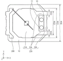
Fig. 1 is a top view of a light-emitting device according to embodiment 1 of the present invention.
Fig. 2A is a top view of the light-emitting device according to embodiment 1 of the present invention, in which the resin frame and the sealing member are omitted.
Fig. 2B is a top view of the light-emitting device according to embodiment 1 of the present invention, in which the sealing member is omitted.
Fig. 3A is a sectional view taken along line a-a of fig. 1.
Fig. 3B is a sectional view taken along line B-B of fig. 1.
Fig. 3C is a cross-sectional view taken along line C-C of fig. 1.
Fig. 4A is a modification of the light-emitting device according to embodiment 1 of the present invention.
Fig. 4B is a modification of the light-emitting device according to embodiment 1 of the present invention.
Fig. 4C is a modification of the light-emitting device according to embodiment 1 of the present invention.
Fig. 4D is a modification of the light-emitting device according to embodiment 1 of the present invention.
Fig. 4E is a modification of the light-emitting device according to embodiment 1 of the present invention.
Fig. 5A is a top view of a light-emitting device according to embodiment 2 of the present invention.
Fig. 5B is a top view of the light-emitting device according to embodiment 2 of the present invention, in which the resin frame and the sealing member are omitted.
Fig. 5C is a cross-sectional view taken along line D-D of fig. 5A.
Fig. 6A is a top view of a light-emitting device according to embodiment 3 of the present invention.
Fig. 6B is a top view of the light-emitting device according to embodiment 3 of the present invention, in which the resin frame and the sealing member are omitted.
Description of the reference numerals
1000. 2000 light-emitting device
10 resin member
11 convex part
20 conductive member
20A first lead
20B second lead
30 base body
31 st surface (1 st surface)
32 nd 2 nd side
40 light emitting element
50 resin frame
60 conducting wire
70 sealing member
71 wavelength conversion member
72 light diffusing member
80 protective element
Detailed Description
The mode for carrying out the present disclosure is explained below with reference to the drawings. However, the following embodiments are merely examples of the light-emitting device for embodying the technical idea of the present disclosure, and the present disclosure is not limited to the following light-emitting device.
In addition, the present specification absolutely does not specify the components shown in the claims as the components of the embodiments. In particular, the dimensions, materials, shapes, relative arrangements of the constituent members described in the embodiments, and the like are not intended to limit the scope of the present disclosure to these unless otherwise specified. In addition, the sizes, positional relationships, and the like of the members shown in the drawings may be exaggerated for clarity of description. In the following description, the same name and reference numeral denote the same member or the same member, and detailed description thereof will be omitted as appropriate.
< embodiment 1>
A light-emitting device 1000 according to embodiment 1 of the present invention will be described with reference to fig. 1, 2A, 2B, and 3A to 3C. The light-emitting device 1000 includes: a light emitting element 40; a first lead 20A including a wide portion 21A on which the light emitting element 40 is mounted, a narrow portion 22A extending from the wide portion and having a width smaller than that of the wide portion 21A, and a terminal portion 23A extending from the narrow portion 22A and having a width larger than that of the narrow portion 22A; a second lead 20B electrically connected to the light emitting element 40; a resin member 10 supporting the first lead 20A and the second lead 20B and including a convex portion 11; and a resin frame 50 surrounding the light emitting element 40 and covering at least a part of the convex portion 11, wherein the resin member 10 includes at least a part of the convex portion 11 at a position surrounded by the wide portion 21A, the narrow portion 22A, and the terminal portion 23A.
As shown in fig. 3A, the base 30 includes a 1 st surface 31 and a 2 nd surface 32 on the opposite side of the 1 st surface 31. As shown in fig. 1, the base 30 includes a conductive member 20 and a resin member 10. The conductive member 20 includes a first lead 20A and a second lead 20B. Resin member 10 supports first lead 20A and second lead 20B. As shown in fig. 2A, the first lead 20A includes a wide portion 21A, a narrow portion 22A, and a terminal portion 23A. The light emitting element 40 is disposed in the wide portion 21A. The narrow portion 22A extends from the wide portion 21A in a direction away from the light emitting element 40. The width W22 of the narrow width part 22A is narrower than the width W21 of the wide width part 21A. The terminal portion 23A is extended from the narrow portion 22A. Width W23 of terminal portion 23A is wider than width W22 of narrow portion 22A. The width W21 of the wide portion 21A, the width W22 of the narrow portion 22A, and the width W23 of the terminal portion 23A are defined as the length of the first lead 20A in the direction perpendicular to the direction in which the narrow portion 22A extends from the wide portion 21A. As shown in fig. 3B, the resin member 10 includes the convex portion 11 on the 1 st surface 31. At least a part of the convex portion 11 is provided at a position surrounded by the wide portion 21A, the narrow portion 22A, and the terminal portion 23A. As shown in fig. 1, the resin frame 50 surrounds the light emitting element 40 and covers at least a part of the projection 11.
Generally, the resin member 10 containing the resin material has higher adhesion to the resin frame 50 than the resin frame 50 has to the conductive member 20 not containing the resin. This is because the thermal expansion coefficients of the resin member 10 and the resin frame 50 can be made close to each other because both the resin member 10 and the resin frame 50 contain resin. Therefore, by increasing the contact area between the resin member 10 and the resin frame 50 having high adhesion, the adhesion between the resin frame 50 and the base 30 can be effectively improved. In the light-emitting device 1000, the resin member 10 includes the convex portion 11, and the convex portion 11 is covered with the resin frame 50. Therefore, the contact area between the resin member 10 and the resin frame 50 can be increased more than in the case where the projection 11 is not provided. This improves the adhesion between the resin frame 50 and the base 30.
The convex portion 11 is provided at a position surrounded by the wide portion 21A, the narrow portion 22A, and the terminal portion 23A. The entire circumference of the convex portion 11 may not be surrounded by the wide portion 21A, the narrow portion 22A, and the terminal portion 23A. For example, as shown in fig. 2A, the first lead wire 20A may not be located on the side of the projection 11 opposite to the side where the narrow-width portion 22A is located. By providing the convex portion 11 at a position surrounded by the wide portion 21A, the narrow portion 22A, and the terminal portion 23A, the convex portion 11 is positioned between the wide portion 21A and the terminal portion 23A. Thus, the width W30 of the base 30 is hardly widened. For example, in the case where the convex portion 11 is formed in the direction perpendicular to the direction in which the narrow portion 22A extends from the wide portion 21A from the narrow portion 22A, the width W30 of the base 30 is more difficult to be wider than in the case where the convex portion 11 is formed in the direction perpendicular to the direction in which the narrow portion 22A extends from the wide portion 21A and/or the terminal portion 23A. This facilitates miniaturization of the light-emitting device. The width W30 of the base 30 is the length of the base 30 in the direction perpendicular to the direction in which the narrow portion 22A extends from the wide portion 21A.
The convex portion 11 is preferably provided at a position separated from the wide portion 21A and the terminal portion 23A. This can increase the contact area between the resin frame 50 and the resin member 10, thereby improving the adhesion between the resin frame 50 and the base 30.
In the light-emitting device 1000, the shape of the convex portion 11 is a cylinder. In the case where the shape of the convex portion 11 is a cylinder, it is easy to form. The shape of the convex portion 11 may be any shape such as a hemisphere, a cone, a pyramid such as a triangular pyramid, a rectangular pyramid, or a pentagonal pyramid, or a prism such as a triangular prism, a rectangular prism, or a pentagonal prism. As shown in fig. 4A, the surface of the convex portion 11 at the portion covered with the resin frame 50 may have irregularities. The contact area between the convex portion 11 and the resin frame 50 can be increased as compared with the case where the surface of the convex portion 11 does not have the concave-convex portions. This improves the adhesion between the resin frame 50 and the base 30.
As shown in fig. 3B, when the projection 11 includes the upper surface 12 and the side surface 13, the resin frame 50 preferably covers the upper surface 12 and the side surface 13 of the projection 11. Since the resin frame 50 is covered with the upper surface 12 and the side surfaces 13, the contact area between the resin frame 50 and the convex portions 11 can be increased as compared with the case where the resin frame 50 is covered with only the side surfaces 13 of the convex portions 11, and thus the adhesion between the resin frame 50 and the base 30 can be improved.
In fig. 2B, a portion of the conductive member 20 covered with the resin frame 50 is hatched. The shortest distance W11 between the portion of first lead 20A covered with resin frame 50 and the portion of projection 11 covered with resin frame 50 is preferably within 1 mm. By positioning the projection 11 having high adhesion to the resin frame 50 in the vicinity of the conductive member 20 having low adhesion to the resin frame 50, adhesion between the resin frame 50 and the base 30 can be improved.
Further, the shortest distance W11 between the portion of first lead 20A covered with resin frame 50 and the portion of projection 11 covered with resin frame 50 is preferably shorter than the width of resin frame 50. This improves the adhesion between the resin frame 50 and the base 30. In the present specification, the width of the resin frame 50 is defined as the shortest distance between the inner edge and the outer edge of the resin frame 50.
The number of the projections 11 may be 1 or more. Since the plurality of projections 11 increase the contact area between the projections 11 and the resin frame 50, the adhesion between the resin frame 50 and the base 30 can be improved. As shown in fig. 2B and 3B, the resin member 10 of the light-emitting device 1000 includes 2 convex portions 11. First lead 20A is located between 2 convex portions 11, and is arranged to extend from one convex portion 11 to the other convex portion 11 to form resin frame 50. In this way, since the convex portions 11 having high adhesion to the resin frame 50 are located on both sides of the first lead 20A having low adhesion to the resin frame 50, adhesion between the resin frame 50 and the base 30 can be improved.
The thickness of the projection 11 is preferably 0.4 times or more and less than 1 time the thickness of the resin frame 50. By setting the thickness of the projection 11 to 0.4 times or more the thickness of the resin frame 50, the area of the side surface 13 of the projection 11 is increased. This can increase the contact area between the side surface 13 of the projection 11 and the resin frame 50, thereby improving the adhesion between the projection 11 and the resin frame 50. Further, by making the thickness of the convex portion 11 less than 1 time the thickness of the resin frame 50, the upper surface 12 of the convex portion 11 can be covered with the resin frame 50. This can increase the contact area between the convex portion 11 and the resin frame 50, thereby improving the adhesion between the convex portion 11 and the resin frame 50. In the case where the convex portions 11 are pyramid-shaped, the vertex points of the convex portions 11 can be covered by making the thickness of the convex portions 11 less than 1 time the thickness of the resin frame 50, and therefore the contact area between the convex portions 11 and the resin frame 50 can be increased.
As shown in fig. 4B, the resin frame 50 preferably covers the entire surface of the projection 11. In this way, since the contact area between the convex portion 11 and the resin frame 50 can be increased, the adhesion between the convex portion 11 and the resin frame 50 can be improved. The thickness of the projection 11 is the longest length of the projection 11 in the z direction.
It is preferable that the reflectance of the resin frame 50 at the peak wavelength of the light emitting element 40 is higher than the reflectance of the resin member 10 at the peak wavelength of the light emitting element 40. In this way, since light from the light emitting element 40 is easily reflected by the resin frame 50, the light extraction efficiency of the light emitting device can be improved.
As shown in fig. 3C, the light emitting element 40 and the second lead 20B are electrically connected by a wire 60. Preferably, the connection portion between the lead wire 60 and the second lead 20B is covered with the resin frame 50. This can suppress absorption of light from the light emitting element 40 by the wire 60.
As shown in fig. 2B, the resin frame 50 is disposed across the narrow portion 22A. In this way, the contact area between the resin frame 50 and the resin member 10 can be increased as compared with the case where the resin frame 50 is disposed across the wide portion 21A and/or the terminal portion 23A, and thus the adhesion between the resin frame 50 and the base 30 can be improved.
The inner edge and the outer edge of the resin frame 50 may have a polygonal shape such as a circle, an ellipse, a square, a hexagon, or an octagon, or may have various shapes such as a chamfered corner, in a top view. As shown in fig. 1, the inner edge and the outer edge of the resin frame 50 are preferably formed by chamfering the corners of a rectangle. By chamfering the corner portion of the inner edge of the resin frame 50, an uncured sealing member 70 described later is easily filled in the corner portion in the resin frame 50.
The cross section of the resin frame 50 has a convex shape with a rounded tip. A syringe holding the resin frame before curing therein is prepared, and the resin frame before curing is discharged from a needle having a through hole attached to the tip of the syringe, whereby the resin frame 50 having a curved inner surface and an outer surface can be formed.
As shown in fig. 3A, the thickness H of the resin frame 50 is preferably larger than the thickness of the light emitting element 40. Thus, the sealing member 70 formed in the resin frame 50 easily covers the upper surface of the light emitting element 40. The width W of the resin frame 50 is preferably 0.2 to 5 times the thickness H of the resin frame 50. If the width W of the resin frame 50 is smaller than the thickness H by 0.2 times, the strength of the resin frame 50 is reduced. When the width W of the resin frame 50 is larger than 5 times the thickness H in the z direction, the distance between the resin frame 50 and the light emitting element 40 becomes short, and a part of the light from the light emitting element 40 is easily absorbed. In the present specification, the thickness H of the resin frame 50 is defined as the longest length of the resin frame 50 in the z direction. The thickness of the light emitting element 40 is the longest length of the light emitting element 40 in the z direction.
The surface of the resin frame 50 may be plated. The plating layer may be made of 1 or 2 or more metals such as silver, aluminum, copper, gold, and the like. The plating is preferably made of silver, and all of the plating may be silver. Thus, the light extraction efficiency can be improved.
The sealing member 70 is disposed in a region surrounded by the resin frame 50, and seals the light emitting element 40. This protects the light-emitting element 40. When the surface of the light emitting element 40 has a protective film, the sealing member 70 may seal the light emitting element 40 with the protective film interposed therebetween.
As shown in fig. 4C, the seal member 70 is preferably formed to have a thicker central portion than an outer peripheral portion. By forming the convex shape in which the central portion is thicker than the outer peripheral portion, reflection of light from the light emitting element 40 at the interface between the sealing member 70 and the air is suppressed, and thus the light extraction efficiency can be improved. The convex sealing member 70 having a central portion thicker than an outer peripheral portion can be formed by a dropping method.
As shown in fig. 4D, the wavelength conversion member 71 may be included in the sealing member 70. The wavelength conversion member 71 is a member that converts the wavelength of light of a first peak wavelength emitted by the light emitting element 40 into light of a second peak wavelength different in wavelength from the first peak wavelength. By including the wavelength conversion member 71 in the sealing member 70, it is possible to output mixed light in which the light of the first peak wavelength emitted from the light emitting element 40 and the light of the second peak wavelength emitted from the wavelength conversion member 71 are mixed. For example, when a blue LED is used for the light emitting element 40 and a phosphor such as YAG is used for the wavelength conversion member 71, a light emitting device can be configured to output white light obtained by mixing the blue light of the blue LED and yellow light emitted from the phosphor excited by the blue light.
The wavelength conversion member 71 may be uniformly dispersed in the sealing member 70, or may be non-uniform in the sealing member 70. The wavelength conversion member 71 may be more biased to the vicinity of the light emitting element 40 than the upper surface of the sealing member 70. In this way, even if the wavelength conversion member 71 that is not resistant to moisture is used, the sealing member 70 functions as a protective layer, and therefore deterioration of the wavelength conversion member 71 can be suppressed. Examples of the wavelength converting substance that does not tolerate moisture include fluoride-based phosphors such as KSF-based phosphors, sulfide-based phosphors, chloride-based phosphors, silicate-based phosphors, phosphate-based phosphors, and the like.
As shown in fig. 4D, the sealing member 70 may include a light diffuser 72. The light diffuser 72 diffuses light from the light emitting element 40 by reflecting and/or refracting the light by a refractive index difference with the sealing member 70. This can suppress unevenness in luminance in the sealing member 70. In addition, when the sealing member 70 includes the wavelength conversion member 71 and the light diffusing member 72, color unevenness can be suppressed.
In the light-emitting device 1000, 1 light-emitting element 40 is arranged, but a plurality of light-emitting elements 40 may be arranged as shown in fig. 4E. When a plurality of light emitting elements 40 are provided, the light emitting elements 40 may be mounted on both the first lead 20A and the second lead 20B, or all of the plurality of light emitting elements 40 may be mounted on the first lead 20A. It is preferable to place a plurality of light emitting elements 40 only on the first lead 20A because the distance between the light emitting elements 40 can be narrowed and the light emitting device can be downsized. In addition, when the lead 60 electrically connecting one light emitting element 40 of the 2 light emitting elements to the other light emitting element 40 is formed, the distance between the 2 light emitting elements 40 can be narrowed, and therefore, disconnection of the lead 60 can be suppressed.
As shown in fig. 4E, the protective element 80 may be placed on the base 30. The number of the protection elements 80 may be 1 or more. The protective element 80 may be a known element mounted on the light-emitting device.
Preferably, as shown in fig. 4E, the protective member 80 is partially or entirely coated in the resin frame 50. This can suppress absorption of light from the light-emitting element 40 by the protective element 80. In addition, by forming the resin frame 50 from a member having a reflectance with respect to the peak wavelength of the light emitting element 40 higher than that of the protective element 80, the light extraction efficiency of the light emitting device can be improved.
< embodiment 2>
Light-emitting device 2000 according to embodiment 2 of the present invention shown in fig. 5A to 5C is different in the shape of convex portion 11 from light-emitting device 1000 according to embodiment 1. The other points are the same as those in embodiment 1.
In fig. 5B, the conductive member 20 is hatched at the portion covered with the convex portion 11. As shown in fig. 5B and 5C, at least a part of the convex portion 11 is located at a position surrounded by the wide portion 21A, the narrow portion 22A, and the terminal portion 23A, and covers the narrow portion 22A. By covering the narrow-width portion 22A with the convex portion 11, the contact area between the resin frame 50 and the resin member 10 can be increased. This improves the adhesion between the resin frame 50 and the base 30.
Preferably, the convex portion 11 extends in a direction perpendicular to a direction in which the narrow portion 22A extends from the wide portion 21A, and covers the narrow portion 22A. This reduces the area of protruding portion 11 covering first lead 20A. This also increases the contact area between the resin frame 50 and the resin member 10, thereby improving the adhesion between the resin frame 50 and the base 30. The convex portion 11 of the resin member 10 may be disposed across the first lead 20A. In this way, since resin member 10 is formed so as to surround the upper surface and the side surfaces of first lead 20A, the adhesion between first lead 20A and resin member 10 can be improved.
Further, the convex portion 11 is preferably separated from the wide portion 21A and the terminal portion 23A. When the convex portion 11 covering the wide portion 21A and/or the terminal portion 23A is formed, the convex portion 11 is positioned on the upper surface of the wide portion 21A and/or the terminal portion 23A. Therefore, the resin frame 50 can easily cover the wide width portion 21A and/or the terminal portion 23A. Since the width of the wide portion 21A and/or the terminal portion 23A is larger than the width of the narrow portion 22A, the contact area between the resin frame 50 and the conductive member 20 is likely to increase. Therefore, by separating the convex portion 11 from the wide portion 21A and the terminal portion 23A, the contact area between the resin frame 50 and the resin member 10 can be increased, and thus the adhesion between the resin frame 50 and the base 30 can be improved.
< embodiment 3>
Light-emitting device 3000 according to embodiment 3 of the present invention shown in fig. 6A and 6B is different in the shape of conductive member 20 and the position of convex portion 11 from light-emitting device 1000 according to embodiment 1.
As shown in fig. 6B, at least a part of the convex portion 11 is located at a position surrounded by the wide width portion 21A, the narrow width portion 22A, and the terminal portion 23A, and the first lead 20A may have 2 narrow width portions 22A. In such a case, the convex portion 11 is preferably located between the one narrow-width portion 22A and the other narrow-width portion 22A. In this way, the convex portion 11 having high adhesion to the resin frame 50 can improve adhesion between the resin frame 50 and the one narrow portion 22A and the other narrow portion 22A. Further, the entire periphery of at least a part of the side surface of the resin member 10 may be surrounded by the one narrow portion 22A, the other narrow portion 22A, the wide portion 21A, and the terminal portion 23A. In this way, since the entire periphery of the side surface of resin member 10 is surrounded by first lead 20A, the adhesion between first lead 20A and resin member 10 can be improved. In the light-emitting device 3000, the convex portion 11 is located at a position surrounded by the wide portion 21A, the narrow portion 22A, and the terminal portion 23A.
Hereinafter, materials and the like suitable for each constituent member of the light emitting devices of embodiments 1 to 3 will be described.
(base 30)
The base 30 is used to dispose electronic components such as a light-emitting element and a protective element. The base 30 includes a resin member 10 and a conductive member 20.
(resin Member 10)
Examples of the material of the resin member 10 include epoxy resin, silicone resin, BT resin, polyamide resin, polyimide resin, nylon resin, unsaturated polyester resin, and the like. These resin materials may contain a colorant, a filler, a reinforcing fiber, and the like known in the art. When a white filler such as titanium oxide or zinc oxide is used as the colorant, the light extraction efficiency of the light-emitting device can be improved. Further, by containing a black filler such as carbon black having a large heat emissivity, heat from the light-emitting element can be efficiently released. Examples of the filler include silica and alumina. Examples of the reinforcing fiber include glass, calcium silicate, potassium titanate, and the like.
(conductive member 20)
The conductive member 20 is used to apply a voltage from an external power source to an electronic component such as the light emitting element 40. The conductive member 20 includes a first lead 20A and a second lead 20B. The conductive member 20 is preferably plate-shaped without a portion bent in the z direction. By forming the conductive member 20 in a plate shape, the base 30 can be easily formed.
Preferably, the area of first lead 20A is larger than the area of second lead 20B in plan view. Since the light emitting element 40 is mounted on the first lead 20A, the area of the first lead 20A is increased, so that heat generated in the light emitting element 40 is easily conducted to the first lead 20A. This can suppress a temperature rise of the light-emitting element 40, and thus can improve the reliability of the light-emitting device.
The conductive member 20 may protrude from the side surface of the resin member 10. By increasing the volume of the conductive member 20, the heat radiation performance of the light emitting device can be improved. Preferably, the back surface of first lead 20A directly below light-emitting element 40 is exposed from resin member 10. In the case where the lower surface of the light emitting device is mounted on the mounting substrate, heat generated in the light emitting element 40 can be easily conducted to the mounting substrate under the first lead 20A via the first lead 20A exposed from the resin member 10. This can suppress a temperature rise of the light-emitting element 40, and thus can improve the reliability of the light-emitting device.
The conductive member 20 is preferably formed of a material having a relatively high thermal conductivity. For example, by using a material having a thermal conductivity of 200W/(m · K) or more, heat generated in the light-emitting element 40 is easily conducted to the first lead 20A.
The conductive member 20 is preferably formed of a material which is easily punched or cut and has high strength. For example, a single layer or a laminate of a metal such as copper, aluminum, gold, silver, tungsten, iron, or nickel, an alloy thereof, phosphor bronze, or copper containing iron can be used as the substrate.
The conductive member 20 may have a reflective film on the surface. The reflective film can be made of 1 or 2 or more metals such as aluminum, copper, and gold. Silver is particularly preferably used for the reflective film. Thus, the light extraction efficiency of the light emitting device can be improved.
Examples of a method for forming the reflective film on the conductive member 20 include various methods such as a plating method, a vapor deposition method, a sputtering method, and an ion beam assisted vapor deposition method. The film thickness may be any film thickness as long as it can effectively reflect light from the light emitting element 40, and is, for example, about 20nm to 10 μm, preferably about 50nm to 5 μm, and more preferably about 100nm to 3 μm. The thickness and shape of the conductive member can be appropriately set within a range known in the art.
When silver that is easily sulfided is used as the conductive member 20, a protective film is preferably provided on the surface of the conductive member 20. By providing the protective film to suppress vulcanization of the conductive member 20, a decrease in light extraction efficiency of the light-emitting device can be suppressed. As a material of the protective film, an inorganic material such as alumina or silica can be used.
As shown in fig. 3A, the end surface of first lead 20A and/or second lead 20B preferably has irregularities. By providing the irregularities at the portions where first lead 20A and/or second lead 20B contact resin member 10, the contact area between first lead 20A and/or second lead 20B and resin member 10 can be increased. This improves the adhesion between the first lead 20A and/or the second lead 20B and the resin member 10.
(light emitting element 40)
The light emitting element 40 is disposed on the 1 st surface 31 of the first lead 20A. The light-emitting element 40 is a semiconductor element which emits light by applying a voltage, and a known semiconductor element made of a nitride semiconductor or the like can be applied. The light-emitting element has an emission wavelength in the visible region (380 to 780nm) and can be selected from the ultraviolet region to the infrared region. For example, a nitride semiconductor can be used as a light-emitting element having a peak wavelength of 430 to 490 nm. As the nitride semiconductor, In can be used x Al y Ga 1-X-y N (X is more than or equal to 0, Y, X is more than or equal to 0 and Y is less than or equal to 1), and the like. The light emitting element 40 may be disposed on the 1 st surface 31 with a sub mount (submount) interposed therebetween.
The shape of the light emitting element 40 may be any shape such as a polygon such as a triangle, a quadrangle, or a hexagon, or a shape similar thereto in a top view. The light-emitting element 40 may be an element in which a single-sided electrode of an n-electrode and a p-electrode is formed on the same surface side, or may be an element in which a double-sided electrode of an n-electrode and a p-electrode is formed on 2 surfaces (for example, an upper surface and a lower surface) opposite to each other.
When the light emitting element 40 is a single-sided electrode, the 1 st surface 31 of the first lead 20A is mounted face up. The face-up mounting is a method of mounting the surface opposite to the electrode formation surface of the light-emitting element 40 on the substrate 30. The bonding member between light emitting element 40 and first lead 20A may be an insulating bonding member or a conductive bonding member, and a known bonding member may be used. For example, the insulating bonding member may be an epoxy resin, a silicone resin, or a modified resin thereof, and the conductive bonding member may be a conductive paste such as silver, gold, or palladium, a solder such as Au — Sn eutectic, or a solder of a low-melting metal.
When the light emitting element 40 is a double-sided electrode, a known bonding member may be used as a bonding member between the light emitting element 40 and the first lead 20A as long as the bonding member is conductive. Examples of the conductive bonding member include conductive paste such as silver, gold, and palladium, solder such as Au — Sn eutectic, and solder of low-melting point metal. In this case, the light-emitting element 40 and the first lead 20A can be electrically connected by mounting the light-emitting element on the first lead 20A.
(resin frame 50)
The resin frame 50 is provided annularly around the light emitting element 40. Since the resin frame 50 is provided so as to surround the light emitting element 40, the raw material in an uncured state of the sealing member 70 can be left in the resin frame 50. The resin frame 50 is formed by disposing an uncured raw material that forms the base of the resin frame 50 in a region where the resin frame 50 is desired to be formed, and curing the raw material.
Examples of the material of the resin frame 50 include phenol resin, epoxy resin, BT resin, PPA, and silicone resin. In particular, as a material of the resin frame 50, silicone resin excellent in light resistance is preferable. Further, by dispersing powder of a reflective member or the like which hardly absorbs light from the light-emitting element 40 and has a large refractive index difference with respect to the resin serving as the matrix in the resin serving as the matrix, light from the light-emitting element 40 can be efficiently reflected. As the reflective member, for example, titanium oxide, aluminum oxide, zirconium oxide, magnesium oxide can be used. In particular, titanium oxide is preferable because it is relatively stable with respect to moisture and the like and has a high refractive index. The resin frame 50 has a reflectance of 60% or more, preferably 70% or more, with respect to light from the light emitting element 40. In this way, the light reaching the resin frame 50 is less likely to be absorbed by the resin frame 50, and the light extraction efficiency of the light-emitting device can be improved.
(conductor 60)
The light emitting element 40 and the second lead 20B may be electrically connected via a wire 60. The wire 60 can use a metal material excellent in conductivity. As the metal material, gold, aluminum, copper, silver, or the like can be used. As a method of wire bonding, a known method such as ball bonding or wedge bonding can be used.
(sealing member 70)
As a material of the sealing member 70, a resin material having light transmittance, a glass material, or the like can be used. It is particularly preferable to use a resin material for the material of the sealing member 70. Since the resin member 10 and the resin frame 50 each contain a resin material, the sealing member 70 is also made of a resin material, whereby the adhesion between the sealing member 70 and the resin member 10 and the adhesion between the sealing member 70 and the resin frame 50 can be improved. As the resin material of the sealing member 70, a polycarbonate resin, an epoxy resin, a phenol resin, a silicone resin, an acrylic resin, a polymethylpentene resin, a polynorbornene resin, a modified resin thereof, a hybrid resin containing 1 or more of these resins, or the like can be used. In particular, dimethyl silicone resin and benzene silicone resin having excellent light resistance are preferable as the material of the sealing member 70.
(wavelength conversion member 71)
As the wavelength conversion member 71, particles of a fluorescent material that can be excited by light emission from the light emitting element are used. Examples of the phosphor excitable by the blue light emitting element or the ultraviolet light emitting element include a cerium-activated yttrium aluminum garnet phosphor (YAG: Ce), a cerium-activated lutetium aluminum garnet phosphor (LAG: Ce), a europium-and/or chromium-activated calcium alumino silicate phosphor containing nitrogen (CaO-Al) 2 O 3 -SiO 2 : eu, Cr), europium-activated silicate phosphor ((Sr, Ba) 2 SiO 4 : eu), β sialon phosphors, CASN phosphors, SCASN phosphors, and other nitride phosphors; fluoride-based phosphors such as KSF-based phosphors, sulfide-based phosphors, chloride-based phosphors, silicate-based phosphors, phosphate-based phosphors, quantum dot phosphors, and the like. By combining these phosphors with a blue light emitting element or an ultraviolet light emitting element, light emitting devices of various wavelengths can be manufactured.
(light diffusing member 72)
As a material of the light diffusing member 72, titanium oxide, zirconium oxide, aluminum oxide, silicon oxide, or the like can be used. In particular, titanium oxide is preferable because it is relatively stable with respect to moisture and the like and has a high refractive index.
(protective element 80)
Examples of the protective element 80 include a protective circuit and an electrostatic protective element which can prevent a current from flowing in a reverse direction when a voltage is applied to the light-emitting element 40 in the reverse direction, or prevent an overcurrent from flowing through the light-emitting element when a forward voltage higher than an operating voltage of the light-emitting element 40 is applied. In particular zener diodes can be utilized.
It is obvious that the present invention can be arbitrarily applied without departing from the gist of the present invention, although several embodiments according to the present invention have been described above.
Claims (14)
1. A light-emitting device has:
a light emitting element;
a first lead having a wide portion on which the light emitting element is mounted, a narrow portion extending from the wide portion and having a width smaller than that of the wide portion, and a terminal portion extending from the narrow portion and having a width larger than that of the narrow portion;
a second lead electrically connected to the light emitting element;
a resin member supporting the first lead and the second lead and including a convex portion; and
a resin frame surrounding the light emitting element and covering at least a part of the convex portion,
the resin member includes at least a part of the convex portion at a position surrounded by the wide portion, the narrow portion, and the terminal portion,
the convex portion protrudes in a direction perpendicular to a surface of the resin member on which the convex portion is located.
2. The light-emitting device of claim 1,
the resin frame spans the narrow width portion.
3. A light-emitting device has:
a light emitting element;
a first lead having a wide portion on which the light emitting element is mounted, a narrow portion extending from the wide portion and having a width smaller than that of the wide portion, and a terminal portion extending from the narrow portion and having a width larger than that of the narrow portion;
a second lead electrically connected to the light emitting element;
a resin member supporting the first lead and the second lead and including a convex portion; and
a resin frame surrounding the light emitting element and covering at least a part of the narrow portion and the convex portion,
the convex portion is located outside the first lead with respect to the center of the resin member,
the convex portion protrudes in a direction perpendicular to a surface of the resin member on which the convex portion is located.
4. The light-emitting device according to any one of claims 1 to 3,
the convex portion is separated from the wide portion and the terminal portion.
5. The light-emitting device according to any one of claims 1 to 3,
the convex portion covers the narrow width portion.
6. The light-emitting device according to any one of claims 1 to 3,
the convex portion has an upper surface and a side surface, and the upper surface and the side surface are covered with the resin frame.
7. The light-emitting device according to any one of claims 1 to 3,
the shortest distance between the portion of the first lead covered by the resin frame and the portion of the protruding portion covered by the resin frame is shorter than the width of the resin frame.
8. The light-emitting device according to any one of claims 1 to 3,
the thickness of the convex part is more than 0.4 times and less than 1 time of the thickness of the resin frame.
9. The light-emitting device according to any one of claims 1 to 3,
the resin frame covers the entire surface of the projection.
10. The light-emitting device according to any one of claims 1 to 3,
the resin member is provided with 2 of the convex portions,
the first lead is located between the 2 bumps,
the resin frame is disposed so as to extend from one of the convex portions to the other of the convex portions.
11. The light-emitting device according to any one of claims 1 to 3,
the reflectance of the resin frame at the peak wavelength of the light emitting element is higher than the reflectance of the resin member at the peak wavelength of the light emitting element.
12. The light-emitting device according to any one of claims 1 to 3,
the light emitting element and the second lead are electrically connected by a wire, and a connection portion between the wire and the second lead is covered with the resin frame.
13. The light-emitting device according to any one of claims 1 to 3,
the resin frame contains silicone resin.
14. The light-emitting device according to any one of claims 1 to 3,
the shape of the convex part is a cylinder.
Applications Claiming Priority (2)
| Application Number | Priority Date | Filing Date | Title |
|---|---|---|---|
| JP2016-070432 | 2016-03-31 | ||
| JP2016070432A JP6790416B2 (en) | 2016-03-31 | 2016-03-31 | Light emitting device |
Publications (2)
| Publication Number | Publication Date |
|---|---|
| CN107275301A CN107275301A (en) | 2017-10-20 |
| CN107275301B true CN107275301B (en) | 2022-08-02 |
Family
ID=58464303
Family Applications (1)
| Application Number | Title | Priority Date | Filing Date |
|---|---|---|---|
| CN201710204609.4A Active CN107275301B (en) | 2016-03-31 | 2017-03-30 | Light emitting device |
Country Status (4)
| Country | Link |
|---|---|
| US (1) | US10593847B2 (en) |
| EP (1) | EP3226312B1 (en) |
| JP (1) | JP6790416B2 (en) |
| CN (1) | CN107275301B (en) |
Families Citing this family (16)
| Publication number | Priority date | Publication date | Assignee | Title |
|---|---|---|---|---|
| JP6777104B2 (en) * | 2018-01-31 | 2020-10-28 | 日亜化学工業株式会社 | Light emitting device and its manufacturing method |
| JP6777105B2 (en) | 2018-01-31 | 2020-10-28 | 日亜化学工業株式会社 | Manufacturing method of light emitting device |
| JP7037046B2 (en) | 2018-01-31 | 2022-03-16 | 日亜化学工業株式会社 | Light emitting device and its manufacturing method |
| US10873015B2 (en) | 2018-03-01 | 2020-12-22 | Nichia Corporation | Light emitting device and method of manufacturing the light emitting device |
| JP6822442B2 (en) * | 2018-03-01 | 2021-01-27 | 日亜化学工業株式会社 | Light emitting device and its manufacturing method |
| JP6760324B2 (en) | 2018-03-27 | 2020-09-23 | 日亜化学工業株式会社 | Light emitting device |
| JP6879270B2 (en) * | 2018-07-20 | 2021-06-02 | 日亜化学工業株式会社 | Light emitting device |
| JP6975916B2 (en) * | 2018-08-09 | 2021-12-01 | 日亜化学工業株式会社 | Luminescent device |
| KR102646700B1 (en) * | 2018-08-16 | 2024-03-13 | 엘지이노텍 주식회사 | Lighting apparatus |
| JP7181489B2 (en) * | 2019-01-31 | 2022-12-01 | 日亜化学工業株式会社 | Light emitting device and manufacturing method thereof |
| JP7248887B2 (en) * | 2019-02-15 | 2023-03-30 | 日亜化学工業株式会社 | Resin package and light emitting device |
| JP6916450B2 (en) * | 2019-04-01 | 2021-08-11 | 日亜化学工業株式会社 | Light emitting device and its manufacturing method |
| JP7121312B2 (en) * | 2020-03-26 | 2022-08-18 | 日亜化学工業株式会社 | light emitting device |
| US11769862B2 (en) | 2020-03-26 | 2023-09-26 | Nichia Corporation | Light emitting device |
| JP7137084B2 (en) * | 2020-09-02 | 2022-09-14 | 日亜化学工業株式会社 | light emitting device |
| JP2023082632A (en) * | 2021-12-02 | 2023-06-14 | スタンレー電気株式会社 | semiconductor light emitting device |
Citations (3)
| Publication number | Priority date | Publication date | Assignee | Title |
|---|---|---|---|---|
| CN103718314A (en) * | 2011-08-12 | 2014-04-09 | 夏普株式会社 | Light-emitting device |
| CN104078551A (en) * | 2013-03-29 | 2014-10-01 | 日亚化学工业株式会社 | Light emitting device and method of manufacturing the same |
| JP2015115407A (en) * | 2013-12-10 | 2015-06-22 | 三星電子株式会社Samsung Electronics Co.,Ltd. | Light-emitting element wiring board, semiconductor light-emitting device, and method for manufacturing the same |
Family Cites Families (27)
| Publication number | Priority date | Publication date | Assignee | Title |
|---|---|---|---|---|
| JP4307090B2 (en) * | 2003-01-27 | 2009-08-05 | 京セラ株式会社 | Light emitting element storage package and light emitting device |
| DE112006004259A5 (en) * | 2005-11-21 | 2012-09-06 | Seoul Semiconductor Co., Ltd. | Light-emitting element |
| JP2008108836A (en) * | 2006-10-24 | 2008-05-08 | Sharp Corp | Semiconductor light emitting device and method for manufacturing the same |
| JP5236406B2 (en) | 2008-03-28 | 2013-07-17 | ローム株式会社 | Semiconductor light emitting module and manufacturing method thereof |
| KR100888236B1 (en) | 2008-11-18 | 2009-03-12 | 서울반도체 주식회사 | Light emitting device |
| JP2011100862A (en) * | 2009-11-06 | 2011-05-19 | Sanyo Electric Co Ltd | Light-emitting device and method of manufacturing the same |
| TW201128812A (en) | 2009-12-01 | 2011-08-16 | Lg Innotek Co Ltd | Light emitting device |
| KR101064084B1 (en) | 2010-03-25 | 2011-09-08 | 엘지이노텍 주식회사 | Light emitting device package and fabrication method thereof |
| KR101039994B1 (en) * | 2010-05-24 | 2011-06-09 | 엘지이노텍 주식회사 | Light emitting device and light unit having thereof |
| JP5481277B2 (en) | 2010-06-04 | 2014-04-23 | シャープ株式会社 | Light emitting device |
| JP5920333B2 (en) * | 2011-02-28 | 2016-05-18 | 日亜化学工業株式会社 | Light emitting device |
| KR101832306B1 (en) * | 2011-05-30 | 2018-02-26 | 엘지이노텍 주식회사 | Light emitting device pakage |
| JP2012256651A (en) | 2011-06-07 | 2012-12-27 | Mitsubishi Chemicals Corp | Resin package for semiconductor light-emitting device and manufacturing method therefor and semiconductor light-emitting device having resin package |
| KR101830717B1 (en) * | 2011-06-30 | 2018-02-21 | 엘지이노텍 주식회사 | A light emitting device pakage |
| JP2013058739A (en) * | 2011-08-17 | 2013-03-28 | Dainippon Printing Co Ltd | Optical semiconductor device lead frame, optical semiconductor device lead frame with resin, optical semiconductor device, and optical semiconductor device lead frame manufacturing method |
| KR101905535B1 (en) * | 2011-11-16 | 2018-10-10 | 엘지이노텍 주식회사 | Light emitting device and light apparatus having thereof |
| CN104054189B (en) * | 2011-11-17 | 2018-06-26 | 株式会社流明斯 | Light-emitting element package body and the back light unit for including the light-emitting element package body |
| JP2013206895A (en) | 2012-03-27 | 2013-10-07 | Shin Etsu Chem Co Ltd | Substrate for optical semiconductor device, manufacturing method of substrate for optical semiconductor device, optical semiconductor device, and manufacturing method of optical semiconductor device |
| KR101911047B1 (en) * | 2012-07-25 | 2018-10-24 | 삼성디스플레이 주식회사 | Case and display device |
| US20140070235A1 (en) | 2012-09-07 | 2014-03-13 | Peter Scott Andrews | Wire bonds and light emitter devices and related methods |
| KR102019499B1 (en) * | 2012-11-05 | 2019-09-06 | 엘지이노텍 주식회사 | Light emitting device and lighting systme having thereof |
| JP2014120515A (en) * | 2012-12-13 | 2014-06-30 | Shin Etsu Chem Co Ltd | Substrate for optical semiconductor device and method of manufacturing the same, aggregate substrate, and optical semiconductor device and method of manufacturing the same |
| KR102029802B1 (en) * | 2013-01-14 | 2019-10-08 | 엘지이노텍 주식회사 | Light emitting device and light apparatus having thereof |
| JP6303457B2 (en) | 2013-12-04 | 2018-04-04 | 日亜化学工業株式会社 | Light emitting device and manufacturing method thereof |
| JP6487626B2 (en) * | 2014-03-24 | 2019-03-20 | スタンレー電気株式会社 | Semiconductor device |
| JP6274434B2 (en) * | 2014-07-30 | 2018-02-07 | 豊田合成株式会社 | Silicone resin composition and light emitting device using the same |
| JP2016070432A (en) | 2014-09-30 | 2016-05-09 | アイシン・エィ・ダブリュ株式会社 | Friction engagement device and drive transmission device |
-
2016
- 2016-03-31 JP JP2016070432A patent/JP6790416B2/en active Active
-
2017
- 2017-03-29 US US15/473,505 patent/US10593847B2/en active Active
- 2017-03-30 CN CN201710204609.4A patent/CN107275301B/en active Active
- 2017-03-30 EP EP17163854.7A patent/EP3226312B1/en active Active
Patent Citations (3)
| Publication number | Priority date | Publication date | Assignee | Title |
|---|---|---|---|---|
| CN103718314A (en) * | 2011-08-12 | 2014-04-09 | 夏普株式会社 | Light-emitting device |
| CN104078551A (en) * | 2013-03-29 | 2014-10-01 | 日亚化学工业株式会社 | Light emitting device and method of manufacturing the same |
| JP2015115407A (en) * | 2013-12-10 | 2015-06-22 | 三星電子株式会社Samsung Electronics Co.,Ltd. | Light-emitting element wiring board, semiconductor light-emitting device, and method for manufacturing the same |
Also Published As
| Publication number | Publication date |
|---|---|
| JP6790416B2 (en) | 2020-11-25 |
| CN107275301A (en) | 2017-10-20 |
| US10593847B2 (en) | 2020-03-17 |
| JP2017183578A (en) | 2017-10-05 |
| EP3226312A1 (en) | 2017-10-04 |
| EP3226312B1 (en) | 2021-03-24 |
| US20170288104A1 (en) | 2017-10-05 |
Similar Documents
| Publication | Publication Date | Title |
|---|---|---|
| CN107275301B (en) | Light emitting device | |
| US10361347B2 (en) | Light emitting device | |
| JP6524904B2 (en) | Light emitting device | |
| US8723409B2 (en) | Light emitting device | |
| US9666567B2 (en) | Light emitting device having underlying protective element | |
| KR20060107428A (en) | Light-emitting apparatus | |
| JP2011222641A (en) | Light-emitting device | |
| JP6606966B2 (en) | Light emitting device and manufacturing method thereof | |
| US20210343917A1 (en) | Light emitting device | |
| JP5786278B2 (en) | Light emitting device | |
| JP6985615B2 (en) | Luminescent device | |
| JP5899734B2 (en) | Light emitting device | |
| US9564565B2 (en) | Light emitting device, light emitting module, and method for manufacturing light emitting device | |
| US10002996B2 (en) | Light emitting device and method of manufacturing the same | |
| JP6658787B2 (en) | Light emitting device | |
| US11233184B2 (en) | Light-emitting device and method for manufacturing the same | |
| JP7137079B2 (en) | Light emitting device and manufacturing method thereof | |
| JP7181489B2 (en) | Light emitting device and manufacturing method thereof | |
| JP6593062B2 (en) | Light emitting device | |
| JP7137084B2 (en) | light emitting device | |
| JP6974746B2 (en) | Light emitting device and its manufacturing method |
Legal Events
| Date | Code | Title | Description |
|---|---|---|---|
| PB01 | Publication | ||
| PB01 | Publication | ||
| SE01 | Entry into force of request for substantive examination | ||
| SE01 | Entry into force of request for substantive examination | ||
| GR01 | Patent grant | ||
| GR01 | Patent grant |