JP6748940B2 - Image forming device - Google Patents
Image forming device Download PDFInfo
- Publication number
- JP6748940B2 JP6748940B2 JP2016094480A JP2016094480A JP6748940B2 JP 6748940 B2 JP6748940 B2 JP 6748940B2 JP 2016094480 A JP2016094480 A JP 2016094480A JP 2016094480 A JP2016094480 A JP 2016094480A JP 6748940 B2 JP6748940 B2 JP 6748940B2
- Authority
- JP
- Japan
- Prior art keywords
- photoconductor
- life
- unit
- transfer
- image forming
- Prior art date
- Legal status (The legal status is an assumption and is not a legal conclusion. Google has not performed a legal analysis and makes no representation as to the accuracy of the status listed.)
- Active
Links
Images


Landscapes
- Cleaning In Electrography (AREA)
- Control Or Security For Electrophotography (AREA)
- Color Electrophotography (AREA)
Description
本発明は、画像形成装置に関するものである。 The present invention relates to an image forming apparatus.
従来、帯電手段によって帯電処理した感光体表面に露光手段によって形成した静電潜像を現像処理して得られるトナー像を、転写手段によって被転写材に転写処理する画像形成装置が知られている。この種の画像形成装置には、前回の画像形成時の画像に対応した濃淡が生じる残像の発生によって感光体の劣化状態を検出し、その検出結果に基づいて感光体が寿命を迎えたか否かを判定するものがある。 2. Description of the Related Art Conventionally, an image forming apparatus is known in which a toner image obtained by developing an electrostatic latent image formed by an exposing unit on a surface of a photoreceptor charged by a charging unit is transferred to a transfer material by a transfer unit. .. In this type of image forming apparatus, the deterioration state of the photoconductor is detected due to the occurrence of an afterimage that causes light and shade corresponding to the image at the time of the previous image formation, and whether the photoconductor has reached the end of life based on the detection result. There is something to judge.
例えば、特許文献1には、次の画像形成装置が記載されている。この画像形成装置は、所定の転写条件で転写処理が施された感光体表面部分に対して、帯電手段によって所定の条件で帯電処理を施し、この帯電処理後の感光体表面電位(帯電後電位)Vaを測定する。さらに、別の転写条件で転写処理が施された感光体表面部分に対して、帯電手段によって所定の条件で帯電処理を施して、この帯電処理後の感光体表面電位(帯電後電位)Vbを測定する。そして、VaとVbの絶対値の差分値ΔVを算出する。この差分値ΔVは、転写電流や転写電圧の影響度合いの違いによって生じる残像による画質劣化の度合いを示す指標値となり、この差分値ΔVに基づいて感光体の劣化を判断することで、感光体の寿命を判定することができるとしている。
For example,
しかし、特許文献1の画像形成装置では、転写処理を施した後に行われる帯電処理が、上述したような電位差を打ち消すように作用するため、比較的濃淡差の小さな残像に対しては、比較的濃淡差の大きな残像と比べて差分値ΔVが小さくなる。したがって、濃淡差の小さな残像が生じている感光体の帯電後電位の差が、残像の発生していない感光体の帯電後電位の差と同レベルとなってしまうおそれがあり、濃度差の小さな残像の有無を判別しにくかった。
However, in the image forming apparatus of
上述した課題を解決するために、本発明は、回転駆動する感光体と、該感光体の表面を帯電処理する帯電手段と、該帯電処理後の上記感光体表面に静電潜像を形成する露光手段と、該静電潜像に現像処理して得られるトナー像を被転写材に転写処理する転写手段と、を少なくとも有する画像形成装置において、
上記帯電手段により帯電処理を行った感光体表面に対して上記転写手段による定電圧での転写処理中に上記感光体に流れる電流ID、並びに、上記帯電手段により帯電処理を行った感光体表面に対して、上記露光手段により露光処理を行い、上記転写手段による定電圧での転写処理中に上記感光体へと流れる電流ILを計測する電流計測手段と、上記電流IDと上記電流ILとの比較値を算出する電流比較値算出手段と、該比較値に基づいて上記感光体の寿命が到来したか否かを判定する寿命判定手段と、を有することを特徴とするものである。
In order to solve the above-described problems, the present invention provides a photosensitive member that is rotationally driven, a charging unit that charges the surface of the photosensitive member, and an electrostatic latent image is formed on the surface of the photosensitive member after the charging process. In an image forming apparatus including at least an exposing unit and a transferring unit that transfers a toner image obtained by developing the electrostatic latent image to a transfer material,
A current ID flowing through the photoconductor during the transfer process at a constant voltage by the transfer unit on the photoconductor surface charged by the charging unit, and a photoconductor surface charged by the charging unit. On the other hand, a comparison is made between the current ID and the current IL, which is subjected to the exposure processing by the exposure means and measures the current IL flowing to the photoconductor during the transfer processing at the constant voltage by the transfer means. The present invention is characterized by including a current comparison value calculation means for calculating a value, and a life determination means for determining whether or not the photoconductor has reached the end of its life based on the comparison value.
本発明によれば、濃淡差の小さい残像の発生によって到来する感光体の寿命について、その寿命が到来したかどうかを判定することができる。 According to the present invention, it is possible to determine whether or not the life of a photoconductor has arrived due to the occurrence of an afterimage with a small difference in gray level.
〔実施形態1〕
以下、本発明の一実施形態(以下「実施形態1」という。)について説明する。
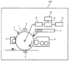
図1は、本実施形態1に係る画像形成装置100の主要部の構成を示す概略図である。
本画像形成装置100は、図中矢印方向に回転するドラム状の感光体1を備えている。感光体1の周囲には、帯電装置2、露光装置3、現像装置4、転写装置5、クリーニング装置6、及び、除電装置7が、感光体回転方向に沿ってこの順序で配置されている。帯電装置2は、感光体の表面を一様に帯電する帯電手段であり、露光装置3は、帯電された感光体の表面をレーザー光で露光して静電潜像を形成する潜像形成手段である。現像装置4は、静電潜像にトナーを付着させて現像する現像手段であり、転写装置5は、現像により得られた感光体上のトナー像を被転写材である記録材としての転写紙上に転写するための転写手段である。クリーニング装置6は、感光体の表面の転写残トナーをクリーニングするクリーニング手段であり、除電装置7は、感光体表面の残留電荷を除去する除電除去手段である。
[Embodiment 1]
Hereinafter, one embodiment of the present invention (hereinafter referred to as "
FIG. 1 is a schematic diagram showing a configuration of a main part of the image forming apparatus 100 according to the first embodiment.
The image forming apparatus 100 includes a drum-
また、感光体1には、感光体1に流れる電流を測定する電流計測部8が配置されている。この電流計測部8は、本実施形態1において後述する電流ID及び電流ILの電流計測手段として機能する。このほか、本画像形成装置100には、電流比較値算出手段、寿命判定手段及び寿命予測手段として機能する寿命判定部9や、経時変化情報記憶手段として機能する記録メモリ10や、判定結果報知手段、予測結果報知手段及び交換報知手段として機能する報知部11なども設けられている。
Further, the
本画像形成装置100で画像形成を行う場合、まず、画像読取部で原稿から読み取られた原画像信号あるいは外部のコンピュータ等で作成された原画像信号が画像処理部に入力され、適切な画像処理が行われる。こうして得られた入力画像信号が露光装置3に入力され、レーザー光を変調する。入力画像信号によって変調されたレーザー光は、帯電装置2により帯電された感光体1の表面に照射される。感光体表面にレーザー光が照射されると、感光体上には入力画像信号に対応した静電潜像が形成される。感光体1上に形成された静電潜像は、現像装置4によりトナーで現像され、感光体上にトナー像が形成される。
When forming an image with the image forming apparatus 100, first, an original image signal read from an original by the image reading unit or an original image signal created by an external computer or the like is input to the image processing unit and appropriate image processing is performed. Is done. The input image signal thus obtained is input to the
感光体1上に形成されたトナー像は、感光体1の図中矢印方向への回転に伴われて、感光体1に対向して配置された転写装置5に向かって搬送される。一方、感光体1と転写装置5との間の転写領域に向かって給紙部から転写紙が搬送され、転写装置5により転写領域へ印加される転写バイアスの作用によって感光体上のトナー像が転写紙上に転写される。トナー像が転写された転写紙は、定着装置に搬送されて熱と圧力を加えられることによってトナー像が定着され、機外に排出される。トナー像の転写紙への転写が終了した感光体1の表面に残留する転写残トナー等の付着物は、クリーニング装置6によりクリーニングされる。さらに、感光体表面の残留電荷が除電装置7により除去されて、1回の画像形成動作が終了する
The toner image formed on the
このような画像形成動作を何十万回、何百万回と繰り返す中で、感光体表面がクリーニングブレードによる摺擦や現像領域での現像剤による摺擦を受けることで摩耗したり、感光体の感光層が帯電と除電の繰り返しによって疲労したりして、感光体が経時劣化する。感光体が劣化することによって、前回の画像形成時の画像(履歴)が感光体上に残存し易くなり、今回の画像形成により作成される画像上に濃淡となって現れる残像という画像劣化が生じる場合がある。残像は、帯電手段による帯電後、直前の画像形成時に露光手段により露光した感光体表面上の箇所(露光箇所)の画像濃度が、直前の画像形成時に露光手段により露光しなかった感光体表面上の箇所(非露光箇所)の画像濃度よりも、次の画像形成時に濃くなるポジ残像と、薄くなるネガ残像とが存在する。 While repeating such an image forming operation hundreds of thousands of times and millions of times, the surface of the photoconductor is abraded by being rubbed by the cleaning blade or the developer in the developing area. The photosensitive layer becomes fatigued due to repeated charging and discharging, and the photoreceptor deteriorates with time. Due to the deterioration of the photoconductor, the image (history) at the time of the previous image formation tends to remain on the photoconductor, resulting in image deterioration called an afterimage that appears as a shade on the image created by the current image formation. There are cases. The afterimage is the image density of a portion (exposure portion) on the surface of the photoconductor exposed by the exposure means at the time of immediately before image formation after charging by the charging means, on the surface of the photoconductor not exposed by the exposure means at the time of immediately before image formation. There is a positive afterimage which becomes darker at the time of the next image formation and a negative afterimage which becomes lighter than the image density at the portion (non-exposed portion).
そこで、本発明者らが鋭意検討を重ねたところ、次のようなことを見出した。すなわち、転写手段によって定電圧が印加される転写領域を感光体表面の非露光箇所が通過する間に転写手段から感光体に流れる電流IDと、転写手段によって定電圧が印加される転写領域を感光体表面の露光箇所が通過する間に転写手段から感光体に流れる電流ILの絶対値の差分値(比較値)ΔIから、感光体の残像について定量評価することが可能であることがわかった。さらに、差分値ΔIが所定の上限値(ΔImax)より大きい場合にネガ残像が発生し、ΔIが所定の下限値(ΔImin)より小さい場合、ポジ残像が発生することがわかった。 Then, the inventors of the present invention conducted extensive studies and found the following. That is, the current ID flowing from the transfer unit to the photoconductor while the unexposed portion of the surface of the photoconductor passes through the transfer region to which the constant voltage is applied by the transfer unit, and the transfer region to which the constant voltage is applied by the transfer unit are exposed. It has been found that it is possible to quantitatively evaluate the afterimage of the photoconductor from the difference value (comparison value) ΔI of the absolute value of the current IL flowing from the transfer unit to the photoconductor while passing through the exposed portion on the body surface. Further, it has been found that when the difference value ΔI is larger than a predetermined upper limit value (ΔImax), a negative afterimage is generated, and when ΔI is smaller than a predetermined lower limit value (ΔImin), a positive afterimage is generated.
本実施形態1では、帯電装置2によって帯電処理した感光体1表面部分に対して、転写装置5により定電圧による転写処理を行い、この転写処理中に転写手段から感光体1に流れる電流IDを電流計測部8で測定する。また、帯電装置2によって帯電処理した感光体1表面部分に対して露光装置3による露光処理をし、この露光箇所に対する転写装置5による定電圧での転写処理中に転写装置5から感光体1へと流れる電流ILを電流計測部8で測定する。その後、IDとILとの絶対値の差分値(比較値)ΔIを算出し、この差分値ΔIに基づいて感光体の寿命を判定したり予測したりする。
In the first embodiment, the surface of the
本実施形態1において、IDは、感光体累積回転数がn回目であるときに、帯電装置2によって帯電処理した感光体1表面部分に対して、転写装置5により定電圧での転写処理を行い、この転写処理中に転写装置5から感光体1に流れる電流である。また、ILは、感光体累積回転数がn+1回目であるときに、帯電装置2によって帯電処理した感光体1表面部分に対して露光装置3による露光処理をし、この露光箇所に対する転写装置5による定電圧での転写処理中に転写装置5から感光体1へと流れる電流である。
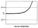
本実施形態1では、図2に示すような感光体累積回転数と標準差分値ΔIとの関係を示す情報(すなわち、所定の環境下において感光体1が寿命に至るまでの標準的な差分値ΔIの経時変化を示す経時変化情報)が記録メモリ10に記憶されている。寿命判定部9は、感光体累積回転数がn回目であるときに測定したIDと、累積回転数がn+1回目であるときに測定したILとを取得し、これらの差分値ΔIを算出したら、その差分値ΔIと寿命判定基準値ΔImax、ΔIminとを比較する。そして、この比較により差分値ΔIが、ΔI<ΔImin、または、ΔI>ΔImaxであると判断したら当該感光体1は寿命を迎えたと判定する。
また、寿命判定部9は、差分値ΔIがΔImin≦ΔI≦ΔImaxであると判断したときは、記録メモリ10内の経時変化情報を参照し、その差分値ΔIと経時変化情報とから、当該感光体が寿命を迎える寿命到達時期を予測する。
In the first embodiment, the ID performs the transfer process at a constant voltage by the transfer device 5 on the surface portion of the
In the first embodiment, information indicating the relationship between the photosensitive member cumulative rotation number and the standard difference value ΔI as shown in FIG. 2 (that is, the standard difference value until the
Further, when the
転写装置5は、定電流制御と定電圧制御の設定切り替えが可能となっており、任意に設定することができる。ただし、ID及びILを測定する際には、定電圧制御に設定される。また、転写装置5による転写処理の条件は、任意に設定することができる。すなわち、画像形成動作時の転写処理の条件とは異なる条件とすることができる。具体的な設定方法としては、例えば、累積回転数n=0のときに、残像の発生しない条件を予め条件を求めておき、常にこの条件で測定を行う方法が挙げられる。 The transfer device 5 can switch between constant current control and constant voltage control, and can be set arbitrarily. However, when measuring ID and IL, constant voltage control is set. Further, the conditions of the transfer processing by the transfer device 5 can be set arbitrarily. That is, the conditions can be different from the conditions of the transfer process during the image forming operation. As a specific setting method, for example, when the cumulative rotation speed n=0, a condition in which an afterimage does not occur is obtained in advance, and measurement is always performed under this condition.
同様に、ID及びILを測定する際の帯電装置2による帯電処理の条件も、任意に設定することができる。すなわち、画像形成動作時の帯電処理の条件とは異なる条件とすることができる。具体的な設定方法としては、例えば、累積回転数n=0のときに、バイアス印加無しで転写領域を通過させた感光体表面部分を帯電処理することで、感光体の表面電位が−600Vとなるような条件を求めておき、常にこの条件で測定を行う方法が挙げられる。また、測定を行う前に、毎回、バイアス印加無しで転写領域を通過させた感光体表面部分を帯電処理することで感光体の表面電位が−600Vとなるような条件を求め、その条件で当該測定における帯電処理を行う方法も挙げられる。
Similarly, the conditions of the charging process by the charging
また、寿命判定や寿命予測を行うための測定は、任意のタイミングで行うことができるが、印刷ジョブ開始時に行うのが好ましい。印刷ジョブと印刷ジョブとの間や、印刷ジョブの終了直後に寿命判定や寿命予測を行うための測定を実行する場合、測定前の印刷ジョブの内容に応じて感光体に蓄積される短期的な劣化の程度が異なるため、測定結果に誤差が生じやすい。 Further, the measurement for determining the life and predicting the life can be performed at any timing, but it is preferable to perform the measurement at the start of the print job. When performing measurements for determining the life and predicting the life between print jobs and immediately after the print jobs are completed, short-term data accumulated on the photoreceptor depending on the contents of the print jobs before measurement Since the degree of deterioration differs, an error is likely to occur in the measurement result.
また、本実施形態1においては、寿命判定部9による感光体の寿命判定結果や寿命予測結果が操作パネル等で構成される報知部11によって報知される。これにより、ユーザー若しくはサービスマンは、報知部11によって報知された情報を基に、適切なタイミングで感光体の交換をすることができる。さらに、ユーザー若しくはサービスマンが、感光体の寿命予測結果の報知を受けることにより、感光体の寿命が到来する前に交換用の感光体を予め手配しておくこともできる。また、感光体のユーザー交換ができない場合においても、感光体の寿命予測結果の報知を受けることで、サービスマンがユーザー先を訪問する計画を効率的に立てることもできるため、画像形成装置100のダウンタイムが低減され、結果として生産性向上に貢献することができる。
In addition, in the first embodiment, the
次に、寿命判定部9で実行される寿命判定・予測工程について説明する。
図3は、本実施形態1の寿命判定・予測工程の処理の流れを示すフローチャートである。
図3に示すように、まず、感光体の累積回転数がn回転目であるときに、IDを測定する(S1)。次いで、感光体の累積回転数がn+1回目であるときに、ILを測定する(S2)。そして、これらの測定値ID,ILから、その差分値ΔI=|(IL−ID)|を算出し(S3)、これを記録メモリ10に記録する(S4)。次に、この差分値ΔIと、予め設定されている寿命判定基準値ΔImax、ΔIminとを比較して、ΔImin≦ΔI≦ΔImaxであるかどうかを判断する(S5)。ΔI<ΔIminまたはΔI>ΔImaxである場合には、感光体の寿命切れと判断し(S6)、報知部11によって感光体の寿命切れを報知する(S7)。
Next, the life judgment/prediction process executed by the
FIG. 3 is a flowchart showing the processing flow of the life determination/prediction process of the first embodiment.
As shown in FIG. 3, first, when the cumulative rotation number of the photoconductor is the nth rotation, the ID is measured (S1). Next, when the cumulative number of rotations of the photoconductor is the (n+1)th time, IL is measured (S2). Then, the difference value ΔI=|(IL-ID)| is calculated from these measured values ID and IL (S3), and this is recorded in the recording memory 10 (S4). Next, this difference value ΔI is compared with preset life judgment reference values ΔImax and ΔImin to judge whether or not ΔImin≦ΔI≦ΔImax (S5). If ΔI<ΔImin or ΔI>ΔImax, it is determined that the life of the photoconductor has expired (S6), and the
定電圧での転写処理の際に、転写手段から感光体に流れる電流の大きさは、感光体軸方向長さや感光体線速にも関係する。感光体軸方向長さが長い方が感光体に流れる電流の大きさは小さくなり、感光体線速が速い方が感光体に流れる電流の大きさは小さくなる。そのため、本実施形態1及び後述の実施形態2(上記変形例を含む)で、IDやILは、定電圧での転写処理の際に転写手段から感光体に流れる電流(μA)/感光体軸方向長さ(mm)/感光体線速(mm/sec)と規定している。よって、ID、IL、ΔI、ΔImax、ΔIminの単位は、μA・sec/mm2となる。 The magnitude of the current flowing from the transfer means to the photoconductor during the transfer process at a constant voltage is also related to the axial length of the photoconductor and the linear velocity of the photoconductor. The larger the axial length of the photoconductor, the smaller the current flowing through the photoconductor, and the faster the linear velocity of the photoconductor, the smaller the current flowing through the photoconductor. Therefore, in the first embodiment and the second embodiment described later (including the above-described modified example), ID and IL are the current (μA) flowing from the transfer means to the photoconductor during the transfer process at a constant voltage/the photoconductor axis. The direction length (mm)/photoconductor linear velocity (mm/sec) is defined. Therefore, the unit of ID, IL, ΔI, ΔImax, and ΔImin is μA·sec/mm 2 .
転写条件や感光体の層構成などにもよるが、寿命判定基準値は、ΔImin≦3.0×10⁻⁴(μA・sec/mm2)、ΔImax≧5.0×10-4(μA・sec/mm2)であるのが好ましい。残像を表現する画像濃度差は、ΔIに依存する傾向があり、通常、ΔIが3.0×10-4(μA・sec/mm2)≦ΔI≦5.0×10-4(μA・sec/mm2)の範囲であれば残像に関して問題はないが、ΔIが3.0×10-4(μA・sec/mm2)≦ΔI≦5.0×10-4(μA・sec/mm2)の範囲外であると残像が無視できないものとなる。 Although it depends on the transfer conditions and the layer structure of the photoconductor, the life judgment reference value is ΔImin≦3.0×10 −4 (μA·sec/mm 2 ), ΔImax≧5.0×10 −4 (μA· It is preferably sec/mm 2 ). The image density difference expressing an afterimage tends to depend on ΔI, and normally ΔI is 3.0×10 −4 (μA·sec/mm 2 )≦ΔI≦5.0×10 −4 (μA·sec) there is no problem with respect to the residual image if / range of mm 2) but, [Delta] I is 3.0 × 10 -4 (μA · sec / mm 2) ≦ ΔI ≦ 5.0 × 10 -4 (μA · sec / mm 2 ) If it is out of the range, the afterimage cannot be ignored.
一方、上記処理ステップ5においてΔImin≦ΔI≦ΔImaxであると判断された場合、まず、IDを測定したときの感光体累積回転数nを記録する(S8)。そして、記録メモリ10に記憶されている図2に示したような感光体累積回転数と標準差分値ΔIとの関係を示す情報(すなわち、感光体が寿命に至るまでの標準差分値ΔIの経時変化情報)を参照して、ΔI=ΔIminもしくはΔI=ΔImaxとなるときの感光体の累積回転数(寿命到達累積回転数)を算出し、算出した寿命到達累積回転数を感光体の寿命到達時期の予測値とする(S9)。そして、算出した寿命到達累積回転数と上記処理ステップ8において記録した感光体累積回転数nとから、今後何枚印刷を行ったら感光体が寿命に至るといった残寿命を判断し、その判断結果を報知部11によってユーザーやサービスマンに報知する(S10)。
On the other hand, if it is determined in the processing step 5 that ΔImin≦ΔI≦ΔImax, first, the photosensitive member cumulative rotation number n when the ID is measured is recorded (S8). Information indicating the relationship between the photosensitive member cumulative rotation number and the standard difference value ΔI stored in the
一般に、上記差分値ΔIは、感光体の劣化に従って上昇する傾向を示すが、感光体の累積回転数の増加に対して一定の割合で増加するとは限らない。例えば、図2に示した本実施形態1の場合のように、感光体累積回転数に対して差分値ΔIが指数関数的に増加する傾向を示す場合もある。また、感光体累積回転数に対して差分値ΔIが減少する傾向を示す場合もある。そのため、画像形成装置の開発段階において、感光体が実際に寿命に至るまでに、感光体累積回転数の増加に従って差分値ΔIがどのような挙動を示すかという標準差分値ΔVの経時変化情報を調べておき、その経時変化情報に基づいて感光体の寿命判定や寿命予測を行うのが、より正確な寿命判定や寿命予測を実現できる点で好ましい。 Generally, the difference value ΔI tends to increase as the photoconductor deteriorates, but it does not always increase at a constant rate with respect to the increase in the cumulative rotation speed of the photoconductor. For example, as in the case of the first embodiment shown in FIG. 2, there is a case where the difference value ΔI tends to exponentially increase with respect to the cumulative rotation speed of the photoconductor. In some cases, the difference value ΔI tends to decrease with respect to the cumulative rotation speed of the photoconductor. Therefore, in the development stage of the image forming apparatus, information on how the standard difference value ΔV changes over time, indicating how the difference value ΔI behaves as the cumulative rotation speed of the photosensitive member increases until the photosensitive member actually reaches the end of its life. It is preferable that the life of the photoconductor is determined and the life of the photoconductor is predicted based on the information about the change over time, because more accurate life determination and life prediction can be realized.
具体的には、例えば、過去に検出した差分値ΔIの推移から、感光体累積回転数に対する差分値ΔIの傾きを計算し、これを、現時点からの図2に示した記録メモリ10内の経時変化情報を用いた外挿予測若しくは予め把握しておいた感光体累積回転数に対する差分値ΔIの傾きデータ及び予め設定された設定値ΔImin、ΔImaxとを照らし合わせることによって、今後何枚印刷を行ったら感光体が寿命に至るのかといった残寿命を判断することができる。
Specifically, for example, from the transition of the difference value ΔI detected in the past, the slope of the difference value ΔI with respect to the cumulative number of rotations of the photoconductor is calculated, and this is calculated as the elapsed time in the
本実施形態1の寿命判定部9は画像形成装置100に搭載されるものであるが、プロセスカートリッジ方式の画像形成装置においては、そのプロセスカートリッジに寿命判定部9を搭載してもよいし、画像形成装置本体に寿命判定部9を搭載してもよい。プロセスカートリッジの一例を図4に示す。プロセスカートリッジは、感光体1と、帯電装置2、露光装置3、現像装置4、転写装置5、クリーニング装置6、除電装置及び電流計測部8のうちの少なくとも1つとを、支持部材で共通支持したものであって、画像形成装置本体に対して着脱自在に構成された装置(部品)である。
The
〔実施形態2〕
次に、本発明の他の実施形態(以下「実施形態2」という。)について説明する。
上記実施形態1に係る画像形成装置100は、感光体を1つ備えたモノクロ画像形成装置100であったが、本発明は複数の感光体を備えたいわゆるタンデム型のカラー画像形成装置にも同様に適用できる。
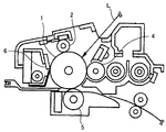
図5は、本実施形態2に係るタンデム型のカラー画像形成装置における主要部の一例を示す概略構成図である。
図5に示すタンデム型のカラー画像形成装置200は、互いに異なる色のトナーを使ってそれぞれの感光体上に各色トナー像を形成し、これらのトナー像を中間転写体である中間転写ベルト20上に互いに重なり合うように1次転写する。そして、中間転写ベルト20上で重なり合った各色トナー像(カラートナー像)は、2次転写ローラ22と対向する2次転写領域で、レジストローラ対21により送り出された転写紙上に2次転写される。カラートナー像が2次転写された転写紙は、転写ベルト23及び搬送ベルト24の表面に担持されながら搬送され、定着装置25で熱と圧力を加えられることによってトナー像が定着され、機外に排出される。
[Embodiment 2]
Next, another embodiment of the present invention (hereinafter referred to as "
The image forming apparatus 100 according to the first embodiment is a monochrome image forming apparatus 100 having one photoconductor, but the present invention is also applicable to a so-called tandem type color image forming apparatus having a plurality of photoconductors. Applicable to
FIG. 5 is a schematic configuration diagram showing an example of a main part of the tandem type color image forming apparatus according to the second embodiment.
The tandem-type color
ここで、タンデム型のカラー画像形成装置の場合、色ごとに個別の感光体が使われるため、複数の感光体を用いる。一般に、出力画像の内容に応じて各色の使われ方が異なるので、そうした状況下で画像形成が繰り返される結果、色ごとに感光体の劣化速度は異なったものとなる。感光体の劣化速度が異なると、感光体の寿命到達時期、つまり感光体の交換時期も異なってくる。そのため、色ごとに、感光体の寿命判定や寿命予測を個別に行う必要がある。このとき、各色それぞれについての感光体交換時期が到来するたびに当該感光体を新たな感光体に交換するようにしてもよいが、この場合、当該画像形成装置全体での感光体交換作業の頻度が高くなり、ユーザーやサービスマンの負担が大きくなる。そこで、本実施形態2においては、以下のような構成により全感光体の交換時期がおおよそ同時期となるようにしてすべての感光体を一括して交換できるように、感光体入れ替え判断工程を実施する。 Here, in the case of a tandem type color image forming apparatus, a plurality of photoconductors are used because a separate photoconductor is used for each color. In general, each color is used differently depending on the content of the output image, and as a result of repeated image formation under such circumstances, the deterioration speed of the photoconductor differs for each color. If the deterioration speed of the photoconductor is different, the life expiration time of the photoconductor, that is, the photoconductor replacement time is also changed. Therefore, it is necessary to individually determine the life of the photoconductor and predict the life of the photoconductor for each color. At this time, the photoconductor may be replaced with a new photoconductor each time the photoconductor replacement time for each color comes, but in this case, the frequency of the photoconductor replacement work in the image forming apparatus as a whole. Becomes higher, and the burden on users and service personnel increases. Therefore, in the second embodiment, the photoconductor replacement determination process is performed so that all the photoconductors can be collectively replaced with the following configuration so that all the photoconductors are replaced at about the same time. To do.
図6は、本実施形態2における感光体入れ替え判断工程の流れを示すフローチャートである。
本実施形態2では、4つの感光体それぞれについて上記実施形態1における図3に示した流れで寿命判定・予測工程と同様の処理を実行する。そして、その工程中の処理ステップ5において、すべての感光体について差分値ΔIと寿命判定基準値ΔImin、ΔImaxとの比較結果がΔImin≦ΔI≦ΔImaxと判断されたとき、上記寿命判定・予測工程中における各感光体の予測結果を報知する処理ステップ10に代えて、図6に示す感光体入れ替え判断工程を実施する。
FIG. 6 is a flowchart showing the flow of the photosensitive member replacement determination process in the second embodiment.
In the second embodiment, the same process as the life determination/prediction process is executed for each of the four photoconductors in the flow shown in FIG. 3 in the first embodiment. Then, in processing step 5 in the process, when the comparison result of the difference value ΔI and the life determination reference values ΔImin and ΔImax for all the photoconductors is ΔImin≦ΔI≦ΔImax, the life determination/prediction process is performed. In place of the
感光体入れ替え判断工程では、まず、図3に示した寿命判定・予測工程中の処理ステップ9において予測した寿命到達時期から判断される各感光体の残寿命に基づき、残寿命が最も短い感光体を特定する(S21)。そして、この感光体の残寿命と予め設定された寿命手前の特定値eとを比較して、この感光体の残寿命が特定値e以下であるかどうかを判断する(S22)。この判断において当該感光体の残寿命が特定値eを超えている場合には、図3に示した寿命判定・予測工程中の処理ステップ10と同様に、残寿命が最も短い感光体の残寿命の判断結果を報知部11によってユーザーやサービスマンに報知する(S23)。なお、感光体ごとの残寿命の判断結果を報知するようにしてもよい。
In the photoconductor replacement determination process, first, the photoconductor with the shortest remaining life is based on the remaining life of each photoconductor judged from the life expiration time predicted in
一方、上記処理ステップ22において、残寿命が最も短い感光体の残寿命が特定値e以下であると判断された場合、次に、各感光体の残寿命に基づいて残寿命が長い感光体を特定する(S24)。そして、上記処理ステップ21で特定した残寿命が最も短い感光体と上記処理ステップ24で特定した残寿命が最も長い感光体とを入れ替えることを促す内容の報知処理を報知部11により行う(S25)。この報知は、残寿命が最も短い感光体と残寿命が最も長い感光体との間で残寿命の差が規定値以上である場合だけ行うようにしてもよい。
On the other hand, when it is determined in the
本実施形態2において、実際の使用環境や使用条件の下で一定期間使用された後に各感光体の残寿命を判断することにより、その実際の使用環境や使用条件下における色ごとの相対的な劣化速度が把握できる。本実施形態2では、残寿命が最も短い感光体の残寿命が特定値eを超えるまでは、所定のタイミングで、残寿命が最も短い感光体と残寿命が最も長い感光体との入れ替えを促す内容の報知処理がなされる。そして、この報知を受けて、ユーザーやサービスマンにより残寿命が最も短い感光体と残寿命が最も長い感光体とが互いに入れ替えられることで、その後は、最も残寿命が残っている感光体が最も劣化速度が速い色について使用され、かつ、最も残寿命が少ない感光体が最も劣化速度が遅い色について使用されることになる。その結果、入れ替え後に当該画像形成装置が一定期間使用されることで、残寿命が最も短い感光体と残寿命が最も長い感光体との間の残寿命差が縮まっていく。 In the second embodiment, by determining the remaining life of each photoconductor after being used for a certain period under the actual use environment or the use condition, the relative use of each color in the actual use environment or the use condition is performed. The deterioration rate can be grasped. In the second embodiment, until the remaining life of the photoconductor having the shortest remaining life exceeds the specific value e, the photoconductor having the shortest remaining life is replaced with the photoconductor having the longest remaining life at a predetermined timing. Content notification processing is performed. In response to this notification, the user or the service person replaces the photoconductor having the shortest remaining life with the photoconductor having the longest remaining life, and thereafter, the photoconductor having the remaining remaining life becomes the most. The photoreceptor having the fastest deterioration rate and the photoreceptor having the shortest remaining life will be used for the color having the lowest deterioration rate. As a result, the image forming apparatus is used for a certain period of time after the replacement, so that the difference in remaining life between the photoreceptor having the shortest remaining life and the photoreceptor having the longest remaining life is reduced.
これにより、このような入れ替えを行わない場合よりも、全感光体の寿命到来時期を互いに近付けることができ、感光体の寿命を多く残したまま交換するというような無駄が少ない状態で、すべての感光体を一括して交換できる。特に、このような感光体入れ替え判断工程を繰り返し行うことで、全感光体の寿命到来時期をほぼ同時期に調整することが可能となるので、より無駄の少ない状態で全感光体の一括交換が可能となる。 As a result, the lifespan of all the photoconductors can be brought closer to each other than in the case where such a replacement is not performed, and all the photoconductors can be replaced with little waste such as leaving the life of the photoconductors long. You can replace the photoconductors at once. In particular, by repeating such a photoconductor replacement determination step, it is possible to adjust the lifespan of all photoconductors at approximately the same time, so it is possible to replace all photoconductors in a batch with less waste. It will be possible.
〔変形例〕
次に、上記実施形態1及び上記実施形態2における一変形例について説明する。
画像形成装置に用いられる感光体は、上述したように、繰り返される画像形成の中で様々なダメージを受けて劣化する。また、感光体は画像形成時以外でも、例えば急激な環境変化(温度および/又は湿度の変化)や、装置内に残存した放電生成物の付着などによるダメージを受ける。これらのダメージによって感光体の劣化状態が通常の感光体劣化推移から大きく逸脱し、感光体の劣化が突発的に進んだ状態になることがある。しかしながら、このような突発的な感光体の劣化は、画像形成動作やリフレッシュ動作などが行われることで、例えばクリーニングブレードにより感光体表面を摺擦することにより回復する場合がある。そのため、たまたま突発的な感光体劣化時に行った測定に基づく差分値ΔIを用いて感光体の寿命判定・予測工程を行うと、本来の寿命到来時期よりも前に寿命であると判定してしまったり、残寿命の判断誤差が大きくなったりする。本変形例は、このような突発的な感光体の劣化が生じていても精度の高い寿命判定や寿命予測を可能とするものである。
[Modification]
Next, a modification of the first embodiment and the second embodiment will be described.
As described above, the photoconductor used in the image forming apparatus is damaged by various damages during repeated image formation and deteriorates. Further, the photoreceptor is damaged even when the image is not formed, for example, due to a rapid environmental change (change in temperature and/or humidity) or adhesion of discharge products remaining in the apparatus. Due to these damages, the deterioration state of the photoconductor may largely deviate from the normal deterioration transition of the photoconductor, and the deterioration of the photoconductor may suddenly progress. However, such a sudden deterioration of the photosensitive member may be recovered by rubbing the surface of the photosensitive member with, for example, a cleaning blade when an image forming operation or a refresh operation is performed. Therefore, if the lifespan determination/prediction process of the photoconductor is performed using the difference value ΔI based on the measurement performed when the photoconductor happens to suddenly deteriorate, it is determined that the life is reached before the actual lifespan is reached. Or, the judgment error of remaining life becomes large. The present modified example enables highly accurate life determination and life prediction even if such a sudden deterioration of the photoconductor occurs.
図7は、図3に示した寿命判定・予測工程中の処理ステップ3と処理ステップ4の間に挿入される本変形例に係る追加処理工程を示すフローチャートである。
図3に示した寿命判定・予測工程中の処理ステップ3で差分値ΔIを算出したら、まず、図2に示した記録メモリ10内の経時変化情報(累積回転数に対する標準差分値ΔIの推移)から、今回の測定時である累積回転数nに対応した標準差分値ΔInを算出する(S31)。そして、差分値ΔIと標準差分値ΔInとの差を算出し、その算出結果と予め設定された設定値fとを比較する(S32)。この比較において|ΔI−ΔIn|≦fである場合には、そのまま上記処理ステップ4に進み、上記処理ステップ3で算出した差分値ΔIを記録メモリ10に記録し、その差分値ΔIに基づいて寿命判定や寿命予測が行われる。
FIG. 7 is a flowchart showing an additional processing step according to the present modification, which is inserted between
When the difference value ΔI is calculated in the
一方、上記処理ステップ32の比較において|ΔI−ΔIn|≦fでない場合には、β時間経過後に(S33)、図2に示した記録メモリ10内の経時変化情報から、前回の測定時における累積回転数nに対し、β時間経過するまでに感光体が回転した感光体回転数αを加算した累積回転数m(すなわちm=n+α)に対応した標準差分値ΔImを算出する(S34)。ここでは、β時間経過後に標準差分値ΔImを算出する場合であるが、図8に示すように感光体回転数がα回転した後に標準差分値ΔImを算出するようにしてもよい。
On the other hand, if |ΔI−ΔIn|≦f does not hold in the comparison in the
このようにして標準差分値ΔImを算出したら、感光体累積回転数がm回転目であるときに、帯電手段によって帯電処理した感光体表面部分に対して、転写手段により定電圧での転写処理を行い、この転写処理中に転写手段から感光体に流れる電流ID’を測定する(S35)。次いで、感光体の累積回転数がm+1回目であるときに、帯電手段によって帯電処理した感光体表面部分に対して露光手段による露光処理をし、この露光箇所に対する転写手段による定電圧での転写処理中に転写手段から感光体へと流れる電流IL’を測定する(S36)。そして、これらの測定値ID’,IL’から、その差分値ΔI=|(IL’−ID’)|を算出し(S37)、これを記録メモリ10に記録する(S4)。そして、以後の処理には、上記処理ステップ37で算出した差分値ΔIを用いて寿命判定や寿命予測を行う。なお、累積回転数nおよび累積回転数mに関して、nは自然数、mはn+2以上の自然数である。また、αは自然数である。
When the standard difference value ΔIm is calculated in this way, when the cumulative number of rotations of the photoconductor is the mth rotation, a transfer process at a constant voltage is performed by the transfer unit on the surface of the photoconductor charged by the charging unit. Then, the current ID′ flowing from the transfer means to the photoconductor during the transfer process is measured (S35). Next, when the cumulative number of rotations of the photoconductor is m+1, the exposure process is performed on the surface part of the photoconductor charged by the charging unit by the exposure unit, and the exposure unit is transferred by a constant voltage by the transfer unit. A current IL' flowing from the transfer means to the photoconductor is measured (S36). Then, the difference value ΔI=|(IL'-ID')| is calculated from these measured values ID' and IL' (S37), and this is recorded in the recording memory 10 (S4). Then, in the subsequent processing, the life determination and the life prediction are performed using the difference value ΔI calculated in the
ここで、時間βは、感光体の一時的な劣化が回復するために必要な時間以上に設定されるものであり、回転数αは一時的な劣化が回復するために必要な感光体回転数である。これらの値β,αは、短期間(あるいは感光体を数回回転させるだけ)で回復する場合や、長期間経過しないと回復しない場合もあるので、適宜設定される。ここで、長期間経過しないと回復しない場合は、例えば感光体を暖める、感光体表面にトナーを入力しながら感光体を回転させて感光体表面を強制的に磨耗させるなど、感光体を回復させるためのリフレッシュ処理を加えてもよい。
なお、差分値ΔIと標準差分値ΔInとの差を算出した際、その算出結果が大きいときには、その旨を報知部11によってユーザーやサービスマンに報知するようにしてもよい。
Here, the time β is set to be equal to or longer than the time required to recover the temporary deterioration of the photoconductor, and the rotation speed α is the rotation speed of the photoconductor required to recover the temporary deterioration. Is. These values β and α may be recovered in a short period of time (or simply by rotating the photoconductor several times) or may not be recovered after a long period of time, and are thus set appropriately. Here, if it does not recover after a long period of time, the photoconductor is recovered, for example, by warming the photoconductor or rotating the photoconductor while inputting toner to the photoconductor surface to forcibly wear the photoconductor surface. Refreshing process may be added.
In addition, when the difference between the difference value ΔI and the standard difference value ΔIn is calculated, and the calculation result is large, the
以上に説明したものは一例であり、次の態様毎に特有の効果を奏する。
(態様A)
回転駆動する感光体1等の感光体と、該感光体の表面を帯電処理する帯電装置2等の帯電手段と、該帯電処理後の上記感光体表面に静電潜像を形成する露光装置3等の露光手段と、該静電潜像に現像処理して得られるトナー像を被転写材に転写処理する転写装置5等の転写手段と、を少なくとも有する画像形成装置100等の画像形成装置において、上記帯電手段により帯電処理を行った感光体表面に対して上記転写手段による定電圧での転写処理中に上記感光体に流れる電流ID、並びに、上記帯電手段により帯電処理を行った感光体表面に対して、上記露光手段により露光処理を行い、上記転写手段による定電圧での転写処理中に上記感光体へと流れる電流ILを計測する電流計測部8等の電流計測手段と、上記電流IDと上記電流ILとの差分値ΔI等の比較値を算出する寿命判定部9等の電流比較値算出手段と、該比較値に基づいて上記感光体の寿命が到来したか否かを判定する寿命判定部9等の寿命判定手段と、を有することを特徴とする。
What has been described above is an example, and the following unique effects can be obtained.
(Aspect A)
A photoconductor such as a
感光体が劣化することによって生じる残像には、画像形成動作中における帯電手段による感光体表面の帯電後、直前の画像形成時に露光手段により露光した感光体表面上の箇所(露光箇所)の画像濃度が、直前の画像形成時に露光手段により露光しなかった感光体表面上の箇所(非露光箇所)の画像濃度よりも、次の画像形成時に濃くなるポジ残像と、薄くなるネガ残像とが存在する。
本発明者らが鋭意検討を重ねたところ、次のようなことを見出した。すなわち、転写手段によって定電圧が印加される転写領域を感光体表面の非露光箇所が通過する間に転写手段から感光体に流れる電流IDと、転写手段によって定電圧が印加される転写領域を感光体表面の露光箇所が通過する間に転写手段から感光体に流れる電流ILの絶対値の差分値(比較値)ΔIから、感光体の残像について定量評価することが可能であることがわかった。
Afterimages caused by the deterioration of the photoconductor include the image density of a portion (exposed portion) on the surface of the photoconductor exposed by the exposure means during the immediately preceding image formation after the surface of the photoconductor is charged by the charging means during the image forming operation. However, there is a positive afterimage that becomes darker at the time of the next image formation and a negative afterimage that becomes darker than the image density at the portion (non-exposed portion) on the surface of the photoconductor that was not exposed by the exposure means during the immediately previous image formation. ..
The present inventors have made extensive studies and found the following. That is, the current ID flowing from the transfer unit to the photoconductor while the unexposed portion of the surface of the photoconductor passes through the transfer region to which the constant voltage is applied by the transfer unit, and the transfer region to which the constant voltage is applied by the transfer unit are exposed. It has been found that it is possible to quantitatively evaluate the afterimage of the photoconductor from the difference value (comparison value) ΔI of the absolute value of the current IL flowing from the transfer unit to the photoconductor while passing through the exposed portion on the body surface.
本態様においては、感光体表面の非露光箇所に対して転写手段による定電圧での転写処理中に感光体に流れる電流IDと、感光体表面の露光箇所に対して転写手段による定電圧での転写処理中に上記感光体へと流れる電流ILとの比較値に基づいて感光体の寿命判定を行っている。このため、残像による画像劣化の度合いを示す指標値が、転写処理後の帯電処理による影響を受けないので、従来の画像形成装置では判別できない濃淡差の小さい残像による画像劣化の度合いを示す指標値とすることができる。したがって、濃淡差の小さい残像の発生によって到来する感光体の寿命を適切に判定することができる。 In this embodiment, the current ID flowing through the photoconductor during the transfer process at the constant voltage by the transfer means to the non-exposed portion on the surface of the photoconductor and the constant voltage by the transfer means to the exposed portion on the surface of the photoconductor. The life of the photoconductor is determined based on the comparison value with the current IL flowing to the photoconductor during the transfer process. Therefore, the index value indicating the degree of image deterioration due to the afterimage is not affected by the charging process after the transfer process, and thus the index value indicating the degree of image deterioration due to the afterimage with a small grayscale difference that cannot be discriminated by the conventional image forming apparatus. Can be Therefore, it is possible to appropriately determine the lifespan of the photoconductor that arrives due to the occurrence of an afterimage with a small grayscale difference.
(態様B)
態様Aおいて、寿命判定部9等の上記寿命判定手段の判定結果を報知する報知部11等の判定結果報知手段を有することを特徴とする。
本態様においては、上記実施形態1及び2について説明したように、画像形成装置のダウンタイムが低減することができる。
(Aspect B)
Aspect A is characterized by including a determination result notifying unit such as a notifying
In this aspect, as described in
(態様C)
態様A又はBの画像形成装置において、複数の感光体を備え、該複数の感光体上に形成された各トナー像を上記被転写材へ転写する構成を有し、電流計測部8等の上記電流計測手段を感光体ごとに設け、寿命判定部9等の上記寿命判定手段は、感光体ごとに寿命が到来したか否かを判定することを特徴とする。
本態様においては、上記実施形態2について説明したように、個々の感光体の劣化速度に応じて各感光体の寿命の到来を適切に判定することができる。
(Aspect C)
The image forming apparatus according to Aspect B has a configuration in which a plurality of photoconductors are provided and each toner image formed on the plurality of photoconductors is transferred to the transfer target material. A current measuring unit is provided for each photoconductor, and the life determining unit such as the
In this aspect, as described in the second embodiment, it is possible to appropriately determine the end of the life of each photoconductor according to the deterioration speed of each photoconductor.
(態様D)
回転駆動する感光体1等の感光体と、該感光体の表面を帯電処理する帯電手段と、該帯電処理後の上記感光体表面に静電潜像を形成する露光装置3等の露光手段と、該静電潜像に現像処理して得られるトナー像を被転写材に転写処理する転写装置5等の転写手段と、を少なくとも有する画像形成装置において、上記帯電手段により帯電処理を行った感光体表面に対する上記転写手段による定電圧での転写処理中に上記感光体に流れる電流ID、並びに、上記帯電手段により帯電処理を行った感光体表面に対して、上記露光手段により露光処理を行い、上記転写手段による定電圧での転写処理中に上記感光体へと流れる電流ILを計測する電流計測部8等の電流計測手段と、
上記電流IDと上記電流ILとの比較値を算出する寿命判定部9等の電流比較値算出手段と、該比較値に基づいて上記感光体の寿命到来時期を予測する寿命判定部9等の寿命予測手段とを有することを特徴とする。
本態様においては、上記実施形態1及び上記実施形態2について説明したように、濃淡差の小さい残像の発生によって到来する感光体の寿命到達時期を適切に予測することができる。
(Aspect D)
A photoconductor such as the
A current comparison value calculating means such as a
In the present aspect, as described in the first and second embodiments, it is possible to appropriately predict the lifespan arrival time of the photoconductor that will arrive due to the occurrence of the afterimage having a small grayscale difference.
(態様E)
態様Dの画像形成装置において、上記感光体が寿命に至るまでの上記比較値の経時変化を示す経時変化情報を記憶する記録メモリ10等の経時変化情報記憶手段を有し、上記寿命予測手段は、上記比較値と、上記経時変化情報とから上記感光体の寿命到来時期を予測することを特徴とする。
本態様においては、上記実施形態1及び上記実施形態2について説明したように、当該画像形成装置における差分値ΔIの推移(経時変化)が特有の経時変化を示す場合でも、高い精度で寿命予測を行うことができる。
(Aspect E)
In the image forming apparatus according to aspect D, a time-dependent change information storage unit such as a
In the present aspect, as described in the first and second embodiments, even when the transition (change with time) of the difference value ΔI in the image forming apparatus shows a characteristic change with time, the life prediction can be performed with high accuracy. It can be carried out.
(態様F)
態様D又はEの画像形成装置において、寿命判定部9等の上記寿命予測手段は、上記比較値の算出に用いた感光体に流れる電流を測定した時期に対応する基準比較値を記録メモリ10等の上記経時変化情報から特定し、該比較値と特定した基準比較値との差が規定値よりも大きいときには、所定期間経過後に改めて電流ID’と電流IL’等の上記電流IDと上記電流ILとの比較値を算出し、該比較値に基づいて感光体の寿命到来時期を予測することを特徴とする。
本態様においては、上記変形例について説明したように、突発的な測定異常による寿命判定ミスや寿命予測ミスを抑制できる。
(Aspect F)
In the image forming apparatus of aspect D or E, the life prediction unit such as the
In the present aspect, as described in the modification, it is possible to suppress the life determination error and the life prediction error due to the sudden measurement abnormality.
(態様G)
態様D〜Fいずれか一の画像形成装置において、寿命判定部9等の上記寿命予測手段の予測結果を報知する報知部11等の予測結果報知手段を有することを特徴とする。
本態様においては、上記実施形態1及び上記実施形態2について説明したように、ユーザーやサービスマンが感光体の寿命到来時期を予測して感光体交換準備を整えることができるので、ダウンタイム低減に有効である。
(Aspect G)
The image forming apparatus according to any one of modes D to F is characterized by having a prediction result notifying unit such as a notifying
In the present aspect, as described in the first and second embodiments, the user and the service person can predict the life expiration of the photoconductor and prepare for the photoconductor replacement, thus reducing downtime. It is valid.
(態様H)
態様D〜Gのいずれか一に記載の画像形成装置において、複数の感光体を備え、該複数の感光体上に形成された各トナー像を上記被転写材へ転写する構成を有し、電流計測部8等の上記電流計測手段を感光体ごとに設け、上記寿命予測手段は、感光体ごとに寿命到来時期を予測することを特徴とする。
本態様においては、上記実施形態2について説明したように、個々の感光体の劣化速度に応じて各感光体の寿命到来時期を適切に予測することができる。
(Aspect H)
The image forming apparatus according to any one of aspects D to G, including a plurality of photoconductors, having a configuration of transferring each toner image formed on the plurality of photoconductors to the transfer material, The current measuring unit such as the measuring unit 8 is provided for each photoconductor, and the life prediction unit predicts the life expiration time for each photoconductor.
In this aspect, as described in the second embodiment, it is possible to appropriately predict the life expiration time of each photoconductor according to the deterioration rate of each photoconductor.
(態様I)
態様Hの画像形成装置において、上記複数の感光体には、互いに入れ替え可能な2以上の感光体が含まれており、上記2以上の感光体のうち上記寿命予測手段により寿命到来時期が最も早いと予測された感光体の寿命到来時期に至る前の所定のタイミングで、該感光体と、該2以上の感光体のうち該寿命予測手段により寿命到来時期が最も遅いと予測された感光体との交換を促す報知を行う交換報知手段を有することを特徴とする。
本態様においては、上記実施形態2について説明したように、より無駄の少ない状態で全感光体の一括交換が可能となる。
(Aspect I)
In the image forming apparatus of aspect H, the plurality of photoconductors include two or more photoconductors that can be replaced with each other, and the life expiration time is earliest by the life prediction means among the two or more photoconductors. At a predetermined timing before the end of the life of the photoconductor predicted to be reached, the photoconductor and, among the two or more photoconductors, the photoconductor predicted to have the latest end of life by the life prediction unit. It is characterized in that it has an exchange informing means for informing the exchange of.
In this mode, as described in the second embodiment, all the photoconductors can be collectively replaced with less waste.
1 感光体
2 帯電装置
3 露光装置
4 現像装置
5 転写装置
7 除電装置
8 電流計測部
9 寿命判定部
10 記録メモリ
11 報知部
20 中間転写ベルト
23 転写ベルト
25 定着装置
100 画像形成装置
200 カラー画像形成装置
DESCRIPTION OF
Claims (9)
上記電流計測手段を感光体ごとに設け、上記寿命予測手段は、感光体ごとに寿命到来時期を予測することを特徴とする画像形成装置。 The image forming apparatus according to any one of claims 4 to 7, further comprising a plurality of photoconductors, each of which is configured to transfer each toner image formed on the plurality of photoconductors onto the transfer target material,
An image forming apparatus, wherein the current measuring means is provided for each photoconductor, and the life prediction means predicts the life expiration time for each photoconductor.
Priority Applications (1)
| Application Number | Priority Date | Filing Date | Title |
|---|---|---|---|
| JP2016094480A JP6748940B2 (en) | 2016-05-10 | 2016-05-10 | Image forming device |
Applications Claiming Priority (1)
| Application Number | Priority Date | Filing Date | Title |
|---|---|---|---|
| JP2016094480A JP6748940B2 (en) | 2016-05-10 | 2016-05-10 | Image forming device |
Publications (3)
| Publication Number | Publication Date |
|---|---|
| JP2017203837A JP2017203837A (en) | 2017-11-16 |
| JP2017203837A5 JP2017203837A5 (en) | 2019-04-04 |
| JP6748940B2 true JP6748940B2 (en) | 2020-09-02 |
Family
ID=60322846
Family Applications (1)
| Application Number | Title | Priority Date | Filing Date |
|---|---|---|---|
| JP2016094480A Active JP6748940B2 (en) | 2016-05-10 | 2016-05-10 | Image forming device |
Country Status (1)
| Country | Link |
|---|---|
| JP (1) | JP6748940B2 (en) |
-
2016
- 2016-05-10 JP JP2016094480A patent/JP6748940B2/en active Active
Also Published As
| Publication number | Publication date |
|---|---|
| JP2017203837A (en) | 2017-11-16 |
Similar Documents
| Publication | Publication Date | Title |
|---|---|---|
| JP5630708B2 (en) | Image forming apparatus | |
| JP6926552B2 (en) | Image forming device, film thickness difference estimation method and management system | |
| US10061250B2 (en) | Image forming apparatus and photoconductor evaluation method | |
| US8019239B2 (en) | Device and method for detecting life of organic photoreceptor and image forming apparatus | |
| JP6971632B2 (en) | Image forming device | |
| JP2020149027A (en) | Image formation device | |
| JP6119262B2 (en) | Image forming apparatus | |
| JP2017207618A (en) | Image forming apparatus and deterioration prediction method | |
| JP2014016559A (en) | Image forming apparatus | |
| JP6748940B2 (en) | Image forming device | |
| JP2009092709A (en) | Image forming apparatus | |
| JP2014228632A (en) | Image forming apparatus and image forming method | |
| JP2002082578A (en) | Image forming method and image forming device | |
| JP2006163118A (en) | Image forming apparatus | |
| JP6915316B2 (en) | Image forming device | |
| JP2020187192A (en) | Image forming apparatus | |
| JP2020013078A (en) | Image forming device | |
| JP6627797B2 (en) | Image forming device | |
| US11892791B2 (en) | Image forming apparatus | |
| JP6900159B2 (en) | Image forming device | |
| US11106152B2 (en) | Image forming apparatus | |
| JP5825842B2 (en) | Image forming apparatus | |
| JP5151099B2 (en) | Image forming apparatus | |
| JP2024061536A (en) | Image forming apparatus | |
| JP6105458B2 (en) | Image forming apparatus |
Legal Events
| Date | Code | Title | Description |
|---|---|---|---|
| A521 | Written amendment |
Free format text: JAPANESE INTERMEDIATE CODE: A523 Effective date: 20190220 |
|
| A621 | Written request for application examination |
Free format text: JAPANESE INTERMEDIATE CODE: A621 Effective date: 20190220 |
|
| A977 | Report on retrieval |
Free format text: JAPANESE INTERMEDIATE CODE: A971007 Effective date: 20191223 |
|
| A131 | Notification of reasons for refusal |
Free format text: JAPANESE INTERMEDIATE CODE: A131 Effective date: 20200110 |
|
| A521 | Written amendment |
Free format text: JAPANESE INTERMEDIATE CODE: A523 Effective date: 20200305 |
|
| TRDD | Decision of grant or rejection written | ||
| A01 | Written decision to grant a patent or to grant a registration (utility model) |
Free format text: JAPANESE INTERMEDIATE CODE: A01 Effective date: 20200710 |
|
| A61 | First payment of annual fees (during grant procedure) |
Free format text: JAPANESE INTERMEDIATE CODE: A61 Effective date: 20200723 |
|
| R151 | Written notification of patent or utility model registration |
Ref document number: 6748940 Country of ref document: JP Free format text: JAPANESE INTERMEDIATE CODE: R151 |