JP6926552B2 - Image forming device, film thickness difference estimation method and management system - Google Patents
Image forming device, film thickness difference estimation method and management system Download PDFInfo
- Publication number
- JP6926552B2 JP6926552B2 JP2017050993A JP2017050993A JP6926552B2 JP 6926552 B2 JP6926552 B2 JP 6926552B2 JP 2017050993 A JP2017050993 A JP 2017050993A JP 2017050993 A JP2017050993 A JP 2017050993A JP 6926552 B2 JP6926552 B2 JP 6926552B2
- Authority
- JP
- Japan
- Prior art keywords
- toner
- image carrier
- film thickness
- image forming
- forming apparatus
- Prior art date
- Legal status (The legal status is an assumption and is not a legal conclusion. Google has not performed a legal analysis and makes no representation as to the accuracy of the status listed.)
- Active
Links
- 238000000034 method Methods 0.000 title claims description 36
- 238000012546 transfer Methods 0.000 claims description 40
- 238000001514 detection method Methods 0.000 claims description 30
- 238000011161 development Methods 0.000 claims description 29
- 230000001186 cumulative effect Effects 0.000 claims description 4
- 239000002344 surface layer Substances 0.000 claims 1
- 230000018109 developmental process Effects 0.000 description 25
- 238000004140 cleaning Methods 0.000 description 11
- 230000006854 communication Effects 0.000 description 8
- 239000000314 lubricant Substances 0.000 description 8
- 238000004891 communication Methods 0.000 description 7
- 230000007423 decrease Effects 0.000 description 7
- 230000007547 defect Effects 0.000 description 4
- 239000003795 chemical substances by application Substances 0.000 description 3
- 108091008695 photoreceptors Proteins 0.000 description 3
- 238000007790 scraping Methods 0.000 description 3
- 239000003086 colorant Substances 0.000 description 2
- 238000003825 pressing Methods 0.000 description 2
- 238000012545 processing Methods 0.000 description 2
- 230000035945 sensitivity Effects 0.000 description 2
- 230000004323 axial length Effects 0.000 description 1
- 239000000969 carrier Substances 0.000 description 1
- 238000013461 design Methods 0.000 description 1
- 238000010586 diagram Methods 0.000 description 1
- 230000000694 effects Effects 0.000 description 1
- 238000012423 maintenance Methods 0.000 description 1
- 238000005259 measurement Methods 0.000 description 1
- 230000006641 stabilisation Effects 0.000 description 1
- 238000011105 stabilization Methods 0.000 description 1
Images


Landscapes
- Control Or Security For Electrophotography (AREA)
Description
本発明は、像担持体の表面膜の膜厚差を推定することができるようにした画像形成装置および膜厚差推定方法、並びに画像形成装置から得られた情報に基づいて当該画像形成装置を管理する管理システムに関するものである。 The present invention uses an image forming apparatus and a film forming difference estimation method capable of estimating the film thickness difference of the surface film of the image carrier, and the image forming apparatus based on the information obtained from the image forming apparatus. It is related to the management system to be managed.
従来から、複写機,プリンター,ファクシミリ及びこれらの複合機などの画像形成装置においては、感光体あるいは転写ベルト等の像担持体の寿命を予測する処理が行われている。この寿命予測処理は、像担持体に電圧を印加したときの電流値を検出して像担持体の表面膜の膜厚を予測し、その結果から像担持体の寿命予測を行うものである。 Conventionally, in image forming devices such as copiers, printers, facsimiles, and multifunction devices thereof, processing for predicting the life of an image carrier such as a photoconductor or a transfer belt has been performed. This life prediction process detects the current value when a voltage is applied to the image carrier, predicts the thickness of the surface film of the image carrier, and predicts the life of the image carrier from the result.
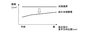
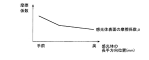
近年、感光体の高耐久化のために、感光体の表面膜の膜厚を、例えば、27.5μmから38.5μmに増大させることが行われている。しかしながら、このように表面膜が厚膜とされた感光体では、図1に示すように、耐久末期において、感光体の長手方向(感光体の回転軸方向)に大きな膜厚傾きが発生する。この膜厚傾きの発生の要因は、図2に示すように、感光体の長手方向の手前側(画像形成装置の正面側)で摩擦係数μが大きくなり、感光体の長手方向の奥側(画像形成装置の背面側)で摩擦係数μが小さくなるためである。 In recent years, in order to increase the durability of the photoconductor, the film thickness of the surface film of the photoconductor has been increased from, for example, 27.5 μm to 38.5 μm. However, in the photoconductor having a thick surface film as described above, as shown in FIG. 1, a large film thickness inclination occurs in the longitudinal direction of the photoconductor (direction of rotation axis of the photoconductor) at the end of durability. As shown in FIG. 2, the cause of this film thickness inclination is that the friction coefficient μ increases on the front side (front side of the image forming apparatus) of the photoconductor in the longitudinal direction, and the friction coefficient μ increases on the back side of the photoconductor in the longitudinal direction (). This is because the coefficient of friction μ becomes smaller on the back side of the image forming apparatus).
感光体の表面膜の摩擦係数の傾きは、感光体上への滑剤の供給によって生じる。一般的には、図3に示すように、前記滑剤の供給においては、トナーに混合することでトナーを介して感光体10Aに滑剤を供給することが行われる。その際にトナーに混合する滑剤の付着強度や大きさによっては、トナーとは遊離した状態で現像剤中に滑剤が存在する場合があり、そのような場合には、現像ローラー13Aから供給される滑剤の量は、トナー搬送方向の下流である感光体10Aの長手方向の手前側において少なくなる。
The slope of the coefficient of friction of the surface film of the photoconductor is caused by the supply of the lubricant onto the photoconductor. Generally, as shown in FIG. 3, in the supply of the lubricant, the lubricant is supplied to the
なお、特許文献1には、感光体の表面膜の減耗傾斜量を算出することが開示されている。この特許文献1では、帯電ローラーを用いる構成において当該帯電ローラーに印可する帯電Vp−pの出力を下げて意図的に帯電不良を発生させ、その帯電不良によるトナー画像の感光体の手前側と奥側とのかぶり量差から傾斜を予測する。しかしながら、かかる構成では、トナー画像のかぶり量の検出のためにIDC(Image Density Control)センサーを、感光体の手前側と奥側の2箇所に設ける構成となる。
In addition,
前記したように、特許文献1に開示の技術では、前記IDCセンサーが感光体の手前側と奥側の2箇所に設ける必要があるため装置価格が割高になるという問題がある。
As described above, in the technique disclosed in
本発明は、像担持体の表面膜の膜厚差を一つの濃度検出部で安価に推定できる膜厚差推定方法、画像形成装置およびこの画像形成装置から得られた情報に基づいて当該画像形成装置を管理する管理システムを提供することを課題とするものである。 The present invention forms the image based on a film thickness difference estimation method, an image forming apparatus, and information obtained from the image forming apparatus, which can inexpensively estimate the film thickness difference of the surface film of the image carrier with one concentration detecting unit. An object of the present invention is to provide a management system for managing the device.
本発明における画像形成装置は、前記の課題を解決するため、表表面が回転移動可能な像担持体と、前記像担持体の表面を帯電させる帯電装置と、前記像担持体上に現像剤を転移させる現像装置と、前記像担持体上の現像剤を第二像担持体上に転写させる転写装置と、前記現像剤のトナーを前記像担持体上に移動させる際に流れる現像電流値を検出する電流検出部と、前記像担持体上の前記回転移動の回転軸方向の異なる2以上の位置に前記現像剤のトナーを用いて2以上のトナーパッチを付与し、前記トナーパッチのうち一つのトナーパッチの濃度を検出する濃度検出部と、前記一つのトナーパッチの濃度を用いて前記像担持体の表面膜における前記回転軸方向の膜厚差を推定する膜厚差推定部とを備え、前記2以上の位置にトナーパッチを形成した時のそれぞれの現像電流値の比と、そのうち一つのトナーパッチの濃度から残りのトナーパッチの濃度を算出するにあたり、前記像担持体上に第1のトナーパッチを形成した際に検出した現像電流値をIg1、前記濃度検出部にて検出した第1のトナーパッチのトナー付着量をρ1、前記回転軸方向で異なる位置に第2のトナーパッチを形成した際に検出した現像電流値をIg2とすると、ρX=(Ig2/Ig1)×(ρ1)の式から、第2のトナーパッチのトナー付着量ρXを推定することを特徴とする。 In the image forming apparatus of the present invention, in order to solve the above problems, an image carrier having a rotatable surface surface, a charging device for charging the surface of the image carrier, and a developer on the image carrier are applied. A developing device for transferring, a transfer device for transferring the developer on the image carrier onto the second image carrier, and a developing current value flowing when the toner of the developer is moved onto the image carrier is detected. Two or more toner patches are applied to two or more positions on the image carrier and two or more positions different in the rotation axis direction of the rotational movement by using the toner of the developer, and one of the toner patches is applied. A density detection unit that detects the density of the toner patch and a film thickness difference estimation unit that estimates the film thickness difference in the rotation axis direction of the surface film of the image carrier using the density of the one toner patch are provided. In calculating the concentration of the remaining toner patches from the ratio of the respective development current values when the toner patches are formed at the two or more positions and the concentration of one of the toner patches, the first one is placed on the image carrier. The development current value detected when the toner patch is formed is Ig1, the toner adhesion amount of the first toner patch detected by the density detection unit is ρ1, and the second toner patch is formed at different positions in the rotation axis direction. Assuming that the development current value detected at this time is Ig2, the toner adhesion amount ρX of the second toner patch is estimated from the equation of ρX = (Ig2 / Ig1) × (ρ1) .
このような構成であれば、前記濃度検出部を複数備える必要がないため、低コストで前記像担持体の表面膜における前記回転軸方向の膜厚差を推定することができる。 With such a configuration, since it is not necessary to provide a plurality of the density detection units, it is possible to estimate the film thickness difference in the rotation axis direction of the surface film of the image carrier at low cost.
前記電流検出部が検出する電流値は、現像剤のトナーを前記像担持体上に転移させる時の現像電流値を検出するようにしている。 Current value the current detection unit detects is to detect the development current value when that transfer toner in the developer on the image bearing member.
ここで、前記2以上の位置にトナーパッチを形成した時のそれぞれの現像電流値の比と、そのうち一つのトナーパッチの濃度から残りのトナーパッチの濃度を算出するようにしている。 Here, and to calculate the concentration of each and the ratio of the developing current value, the remaining toner patch from them the concentration of one of the toner patch when forming a toner patch on the two or more positions.
そして、前記像担持体上に第1のトナーパッチを形成した際に検出した現像電流値をIg1、前記濃度検出部にて検出した第1のトナーパッチのトナー付着量をρ1、前記回転軸方向で異なる位置に第2のトナーパッチを形成した際に検出した現像電流値をIg2とし、
ρX=(Ig2/Ig1)×(ρ1)の式から、第2のトナーパッチのトナー付着量ρXを推定するようにしている。
Then, the developing current value detected when the first toner patch is formed on the image carrier is Ig1, the toner adhesion amount of the first toner patch detected by the concentration detection unit is ρ1, and the direction of the rotation axis. the developing current value detected at the time of forming the second toner patch at different positions in the Ig2,
.rho.x = from the equation (Ig2 / Ig1) × (ρ1 ), so that to estimate the toner adhesion amount .rho.x of the second toner patch.
前記トナーパッチの現像時のトナーパッチの濃度と、このトナーパッチの現像時に流れる現像電流に基づいてトナーの帯電量を検知してもよい。 The amount of charge of the toner may be detected based on the density of the toner patch during the development of the toner patch and the development current flowing during the development of the toner patch.
現像電流値による前記像担持体の表面膜の膜厚差の推定時に検出されたトナー帯電量の値が、所定の範囲内に入っていない場合には前記像担持体の表面膜の膜厚差の推定処理を行わないこととしてもよい。 If the value of the toner charge detected at the time of estimating the film thickness difference of the surface film of the image carrier based on the developing current value is not within a predetermined range, the film thickness difference of the surface film of the image carrier It may be possible not to perform the estimation process of.
また、本発明における他の画像形成装置においては、表面が回転移動可能な像担持体と、前記像担持体の表面を帯電させる帯電装置と、前記像担持体上に現像剤を転移させる現像装置と、前記像担持体上の現像剤を第二像担持体上に転写させる転写装置と、前記像担持体上に転移されたトナーを前記第二像担持体上に転移させる時の転写電流値を検出する電流検出部と、前記像担持体上の前記回転移動の回転軸方向の異なる2以上の位置に前記現像剤のトナーを用いて2以上のトナーパッチを付与し、前記トナーパッチのうち一つのトナーパッチの濃度を検出する濃度検出部と、前記一つのトナーパッチの濃度を用いて前記像担持体の表面膜における前記回転軸方向の膜厚差を推定する膜厚差推定部と、を備えることを特徴とする。 Further, in the other image forming apparatus of the present invention, an image carrier whose surface can be rotated and moved, a charging device that charges the surface of the image carrier, and a developer that transfers a developer onto the image carrier. And a transfer device that transfers the developer on the image carrier onto the second image carrier, and a transfer current value at the time of transferring the toner transferred onto the image carrier onto the second image carrier. Two or more toner patches are applied to two or more positions on the image carrier which are different from each other in the rotation axis direction of the rotational movement, and two or more toner patches are applied using the toner of the developer. A density detection unit that detects the concentration of one toner patch, and a film thickness difference estimation unit that estimates the film thickness difference in the rotation axis direction of the surface film of the image carrier using the density of the one toner patch. It is characterized by having .
本発明における画像形成装置においては、前記像担持体の表面膜における前記回転軸方向の推定した膜厚差と推定時点の累積の前記像担持体の回転数とから、前記像担持体の表面膜の膜厚差の増加傾向を判断して、前記像担持体の寿命予測を行ってもよい。 In the image forming apparatus of the present invention , the surface film of the image carrier is based on the estimated film thickness difference in the rotation axis direction of the surface film of the image carrier and the cumulative number of rotations of the image carrier at the time of estimation. The life of the image carrier may be predicted by judging the increasing tendency of the film thickness difference.
本発明における画像形成装置においては、前記像担持体の表面膜における前記回転軸方向の推定した膜厚差と推定時点の累積の像担持体の回転数とから、前記像担持体の寿命到来を判断するようにしてもよい。 In the image forming apparatus of the present invention , the life of the image carrier is determined from the estimated film thickness difference in the rotation axis direction of the surface film of the image carrier and the cumulative number of rotations of the image carrier at the time of estimation. You may decide.
本発明における画像形成装置においては、前記像担持体の表面膜における前記回転軸方向の推定した膜厚差に基づいて、当該膜厚差を抑制する処理を行ってもよい。 In the image forming apparatus of the present invention, a process of suppressing the film thickness difference may be performed based on the estimated film thickness difference in the rotation axis direction of the surface film of the image carrier.
本発明における画像形成装置においては、前記像担持体の表面膜における前記回転軸方向の推定した膜厚差を抑制する処理としてトナーパッチを生成し、このトナーパッチの生成条件を、推定した膜厚差に基づいて変更するようにしてもよい。 In the image forming apparatus of the present invention , a toner patch is generated as a process of suppressing the estimated film thickness difference in the rotation axis direction in the surface film of the image carrier, and the generation conditions of the toner patch are set to the estimated film thickness. It may be changed based on the difference.
また、この発明の膜厚差推定方法は、本発明における画像形成装置において行う膜厚差推定方法であって、
前記像担持体上の前記回転移動の回転軸方向の異なる2以上の位置に前記現像剤のトナーを用いて2以上のトナーパッチを付与し、前記トナーパッチのうち一つのトナーパッチの濃度を検出し、前記一つのトナーパッチの濃度を用いて前記像担持体の表面膜における前記回転軸方向の膜厚差を推定することを特徴とする。
Further, the film thickness difference estimation method of the present invention is a film thickness difference estimation method performed by the image forming apparatus of the present invention.
Two or more toner patches are applied to two or more positions on the image carrier in different rotation axis directions of the rotational movement using the toner of the developer, and the concentration of one of the toner patches is detected. However, it is characterized in that the difference in film thickness in the rotation axis direction of the surface film of the image carrier is estimated by using the concentration of the one toner patch.
また、この発明の管理システムは、表面が回転移動可能な像担持体と、前記像担持体上の前記回転移動の回転軸方向の異なる2以上の位置に形成した2以上のトナーパッチのうち一つのトナーパッチの濃度を検出する濃度検出部と、を備えた本発明における画像形成装置が管理装置と通信可能に接続された管理システムであって、
前記画像形成装置は、前記管理装置が当該画像形成装置の像担持体の交換時期を管理するための情報として、少なくとも前記一つのトナーパッチの濃度に基づく情報であって、前記像担持体の寿命判定或いは寿命予測に用いる情報を前記管理装置に送信することを特徴とする管理システム。
Further, the management system of the present invention is one of an image carrier whose surface can be rotationally moved and two or more toner patches formed on the image carrier at two or more positions different in the rotational axis direction of the rotational movement. A management system in which an image forming apparatus according to the present invention including a density detection unit for detecting the density of one toner patch is communicably connected to the management device.
The image forming apparatus is information based on the concentration of at least one toner patch as information for the management apparatus to manage the replacement timing of the image carrier of the image forming apparatus, and is the life of the image bearing. A management system characterized in that information used for determination or life prediction is transmitted to the management device.
本発明であれば、像担持体の表面膜の膜厚差を推定するのに用いる濃度検出部を複数備える必要がないため、低コストで像担持体の表面膜の膜厚差を推定することができるという効果を奏する。 According to the present invention, it is not necessary to provide a plurality of concentration detection units used for estimating the film thickness difference of the surface film of the image carrier, so that the film thickness difference of the surface film of the image carrier can be estimated at low cost. It has the effect of being able to.
次に、本発明の実施形態に係る画像形成装置、膜厚差推定方法及び管理システムを添付図面に基づいて具体的に説明する。なお、本発明に係る画像形成装置、膜厚差推定方法及び管理システムは、下記の実施形態に示したものに限定されず、その要旨を変更しない範囲において適宜変更して実施できるものである。 Next, the image forming apparatus, the film thickness difference estimation method, and the management system according to the embodiment of the present invention will be specifically described with reference to the accompanying drawings. The image forming apparatus, the film thickness difference estimation method, and the management system according to the present invention are not limited to those shown in the following embodiments, and can be appropriately modified and implemented without changing the gist thereof.
例えば、図4に示すように、この実施形態に係る画像形成装置100は、トナー画像が形成される4つの厚膜の感光体(像担持体)10に対応させて、現像剤を収容させた4つの現像装置13を設け、各現像装置13においては、それぞれの現像剤中におけるトナーの色彩を異ならせ、黒色,黄色,マゼンダ色,シアン色のトナーを用いるようにしている。
For example, as shown in FIG. 4, the
ここで、この画像形成装置100においては、前記各感光体10を回転させて、各感光体10の表面をそれぞれ帯電装置11によって帯電させ、このように帯電された各感光体10に対して、それぞれ潜像形成装置12により画像形成情報に従った露光を行い、各感光体10の表面にそれぞれ静電潜像を形成するようにしている。上記帯電装置11は、例えば、帯電ローラーを感光体10に接触させて帯電させる。
Here, in the
そして、このように静電潜像が形成された各感光体10に対して、それぞれ対応する現像装置13から所定の色彩のトナーを各感光体10の静電潜像に供給して現像を行い、各感光体10の表面にそれぞれの色彩のトナー画像を形成するようにしている。
Then, each of the
次いで、前記のように各感光体10に形成された各色彩のトナー画像を、回転ローラー14aに架け渡されて回転駆動される無端ベルト状になった中間転写ベルト14の表面に、前記各感光体10と対向して設けられた各一次転写ローラー15により順々に一次転写させて、この中間転写ベルト(第二像担持体)14の表面にフルカラーのトナー画像を形成するようにしている。
Next, the toner images of the respective colors formed on the
また、前記中間転写ベルト14に転写されずに各感光体10の表面に残留しているトナーを、それぞれ第1のクリーニング装置30によって、各感光体10の表面から除去するようにしている。
Further, the toner remaining on the surface of each photoconductor 10 without being transferred to the
そして、前記のように中間転写ベルト14の表面に形成されたフルカラーのトナー画像を、この中間転写ベルト14により二次転写ローラー16と対向する位置に導くようにしている。
Then, the full-color toner image formed on the surface of the
また、画像形成装置100に設けられた給紙装置に積載されている用紙Sを、給紙ローラー41により給紙してタイミングローラー18に送り、このタイミングローラー18により用紙Sを中間転写ベルト14と二次転写ローラー16との間に導き、中間転写ベルト14の表面に形成されたトナー画像を前記二次転写ローラー16により用紙Sに転写させるようにしている。また、用紙Sに転写されずに前記中間転写ベルト14の表面に残ったトナーを、第2のクリーニング装置31によって中間転写ベルト14の表面から除去するようにしている。
Further, the paper S loaded on the paper feed device provided in the
そして、前記のようにトナー画像が転写された用紙Sを定着装置19に導き、この定着装置19により、転写された前記トナー画像を用紙Sに定着させた後、このようにトナー画像が定着された用紙Sを排紙ローラー20により排紙させるようにしている。
Then, the paper S on which the toner image is transferred is guided to the fixing
前記トナー画像が形成される4つの感光体10に対応させて、現像剤を収容させた4つの現像装置13が設けられており、各現像装置13においては、それぞれの現像剤中におけるトナーの色彩を異ならせ、黒色,黄色,マゼンダ色,シアン色のトナーを用いるようにしている。
Four developing
図13には、図4に示した画像形成装置100における或る色についての画像形成部、IDCセンサー1、現像電流検出部2、転写電流検出部3、膜厚推定部(寿命判定/予測)4、通信部5等を示している。IDCセンサー1は、トナー濃度を検出する濃度検出部となり、後述する第1のトナーパッチ側にのみ設けている。現像電流検出部2は、現像時の現像電流値を検出し、転写電流検出部3は、転写時の転写電流値を検出する。膜厚差推定部4(寿命判定/予測)は、画像形成装置100におけるCPU等により構成されており、感光体10の表面膜における回転軸方向の膜厚差を推定する処理、この膜厚差推定に用いるトナー濃度やトナー付着量の算出処理、後述する膜厚消耗率、減耗傾斜増加率、これら情報に基づく感光体10の寿命判断や寿命予測を行う。これら処理の詳細は後述する。通信部5はインターネット等の通信回線を用いて管理装置1000との間で通信を行う。前記通信部5と管理装置1000との通信処理についても後述する。
FIG. 13 shows an image forming unit, an
また、この実施形態では、前記感光体10の帯電電流から当該感光体10の表面膜(感光層)の平均膜厚を推定して寿命予測を行うことに加え、耐久性向上のために表面膜を厚膜化した場合に課題となる減耗傾斜量も検出し、図5に示す感光体回転数と平均膜厚値との関係と、図6に示す感光体回転数と減耗傾斜量の関係の両方を用いて感光体寿命を予測する。なお、図5において、平均膜厚の初期値は、感光体10の設計値でもよいし、帯電電流による予測値でもよい。
Further, in this embodiment, in addition to estimating the average film thickness of the surface film (photosensitive layer) of the photoconductor 10 from the charging current of the
前記減耗傾斜量は、前記感光体10の回転軸方向の膜厚差であって、例えば、感光体10の奥側205〜326mm位置の表面膜の最高膜厚値から感光体10の手前側33〜133mm位置の表面膜の平均膜厚を減算した値と定義することができる。
The amount of depletion inclination is the difference in film thickness in the rotation axis direction of the
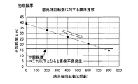
前記図5に示したように、平均膜厚値は当然のごとく耐久が進むほどに低下していくが、前記図6に示したように、前記減耗傾斜量としても耐久が進むほどに増加し、ある上限値を超えると濃度傾き等の画像不良が発生するようになるため、減耗傾斜量の感光体寿命を決める律速となる。 As shown in FIG. 5, the average film thickness value naturally decreases as the durability progresses, but as shown in FIG. 6, the depletion inclination amount also increases as the durability progresses. If a certain upper limit value is exceeded, image defects such as density tilt will occur, so that the rate-determining factor for determining the life of the photoconductor for the amount of wear tilt.
ここで、感光体10の表面膜の膜厚が薄いほど静電容量が大きくなり、多くの露光量が必要となるため、レーザーで同じ露光量で露光した場合には膜厚が薄い側のトナー濃度が薄くなり、感光体10の長手方向(回転軸方向)で膜厚に傾きが生じて減耗傾斜量が大きくなるほど大きな濃度傾きが発生する。例えば、図7に示すように、感光体10の手前から奥のトナー濃度差として0.8以下としたい場合には、感光体10の手前から奥のトナー付着量差として0.8g/m^2以下とする必要がある。一方で、感光体10の手前から奥の減耗傾斜量に対する感光体10の手前から奥のトナー付着量差には、図8に示すように相関があり、減耗傾斜量としては7μm以下としなければ濃度傾きが目立ってしまう。
Here, the thinner the surface film of the
前記の理由により、この実施形態では、感光体10の寿命予測としては感光体10の表面膜の平均膜厚と減耗傾斜量の両方を検出して予測している。感光体10の表面膜の平均膜厚の検出については、帯電装置に所定の電圧を印加した時の帯電電流から検知する既存の検知処理を用いることができる。
For the above reason, in this embodiment, both the average film thickness of the surface film of the
次に、感光体10の減耗傾斜量の検出処理について以下に述べる。上述したように、感光体10の減耗傾斜量において手前から奥の濃度差に相関があるため、感光体10上に例えば下記のようなトナーパッチ画像を作成し、このトナーパッチ画像の濃度を測定することで感光体10の減耗傾斜量を予測することができる。
Next, the processing for detecting the amount of wear inclination of the
ここでは、図9に示すように、例えば、第1のトナーパッチを長手方向の長さが360mmの感光体10の手前端から33mmの箇所に形成し、この第1のトナーパッチを形成したときの現像電流値と、そのトナーパッチ濃度とを検出する。次に、第2のトナーパッチを感光体10の奥側端から33mmの箇所に形成し、この第2のトナーパッチを形成したときの現像電流値を検出する。各トナーパッチは、例えば、感光体10の軸方向上の長さが50mmとされ、周方向の長さが20mmとされた方形形状を有する。前記IDCセンサー1は、前記第1のトナーパッチの濃度を検知できる位置に設けられている。
Here, as shown in FIG. 9, for example, when the first toner patch is formed at a position 33 mm from the front end of the
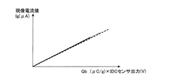
トナーで現像する時に流れる現像電流値は、トナーで現像させたときのトナー付着量(濃度)をIDCセンサーで検出して横軸に取った場合、下記のような特性がある。すなわち、図10に示すように、IDCセンサーの出力が高くなるほど(トナー付着量が多くなるほど)、現像電流値が多く流れ、かつ、現像されるトナーの帯電量にも依存性があり、トナーの帯電量が多いほど現像電流値も多く流れる。従って、図11に示すように、トナーの帯電量とIDCセンサー出力の積算値と現像電流値に比例関係にあり、トナーの帯電量が異なった場合でも、前記積算値と現像電流値は一つのライン上に載る。 The developing current value that flows when developing with toner has the following characteristics when the amount (concentration) of toner adhering when developed with toner is detected by the IDC sensor and taken on the horizontal axis. That is, as shown in FIG. 10, the higher the output of the IDC sensor (the larger the amount of toner adhered), the larger the developing current value flows, and the more the charged amount of the developed toner also depends on the toner. The larger the amount of charge, the larger the development current value. Therefore, as shown in FIG. 11, the integrated value of the toner, the integrated value of the IDC sensor output, and the developing current value are in a proportional relationship, and even if the charged amount of the toner is different, the integrated value and the developing current value are one. Get on the line.
前述の関係を用いて、感光体10上に第1のトナーパッチを作成した際に現像電流検出部2によって検出した現像電流値をIg1、第1のトナーパッチ側にのみIDCセンサー1を設けておいて、現像電流値を検出した際の第1のトナーパッチのトナー付着量をIDCセンサー1で検出し、その時に検出したトナー付着量をρ1とする。続いて奥側に第2のトナーパッチを作成し、その際に検出した現像電流値をIg2とする。第1のトナーパッチと第2のトナーパッチの付与は連続的に行われるため、それぞれのパッチ形成時のトナー帯電量を同等とみなすと、上述した比例関係から、Ig1:Ig2=ρ1:ρXの関係が得られ、この関係からρX=(Ig2/Ig1)×(ρ1)の式が得られることから、第2のトナーパッチのトナー付着量ρXを推定することができる。
Using the above relationship, the development current value detected by the development
第1のトナーパッチのトナー付着量ρ1と、推定された第2のトナーパッチのトナー付着量ρXとから、感光体10の手前から奥のトナー付着量差を推定することができ、図12に示す減耗傾斜量と感光体の手前から奥のトナー付着量差とにおける既知の関係から、減耗傾斜量を推定することができる。例えば、前記第1のトナーパッチのトナー付着量と前記第2のトナーパッチのトナー付着量との差が0.6g/m^2であった場合には、減耗傾斜量は5μmとなり、減耗傾斜量の上限(寿命)が7μmであるとするならば、感光体10が寿命の約70%に到達していると判断することができる。
From the toner adhesion amount ρ1 of the first toner patch and the estimated toner adhesion amount ρX of the second toner patch, the difference in the toner adhesion amount from the front side to the back side of the
トナーパッチの形状は、上述したような20mm×50mm程度の大きさのパッチでも十分検出が可能である。すなわち、手前と奥に形成したトナーパッチの濃度差を検出できれば良いため、トナー付着量についてはハーフトーン濃度でも検出可能であり、また長手方向のパッチ長さも50mm程度もあれば十分検出可能であり、減耗傾斜量を検出時のトナー消費量を抑えることが可能である。もちろん、検出精度を高めるためには現像電流値を多くなるように周方向の長さを20mmではなく、それよりも長くしてもよい。また、トナーパッチの周方向の長さを、感光体一周分(約95mm)にすると、周方向全体の感光体10の長手方向の膜厚差の平均等を得ることができる。
The shape of the toner patch can be sufficiently detected even with a patch having a size of about 20 mm × 50 mm as described above. That is, since it is sufficient to detect the density difference between the toner patches formed in the front and the back, the toner adhesion amount can be detected even with the halftone density, and the patch length in the longitudinal direction can be sufficiently detected if it is about 50 mm. , It is possible to suppress the toner consumption when detecting the amount of depletion inclination. Of course, in order to improve the detection accuracy, the length in the circumferential direction may be longer than 20 mm so as to increase the developing current value. Further, when the length of the toner patch in the circumferential direction is set to one circumference of the photoconductor (about 95 mm), the average film thickness difference in the longitudinal direction of the
また、前記のように現像電流値を用いてトナーパッチの濃度を検出する場合、現像電流値Igはトナー帯電量(Qb)にも比例するため、余りにも帯電量が高い状態(例えば70μC/g以上)の場合にはトナー帯電量の影響を大きく受けるためトナーパッチの濃度差に対する現像電流値Igの差が出にくくなり、トナーパッチ濃度の検出感度(推定精度)が低下する。また、反対に帯電量を著しく低下した状態(例えば20μC/g以下)の場合にはトナー帯電量が低く現像電流値Igの出力自体が小さくなってしまうため、トナーパッチ濃度の検出感度(推定精度)が低下する。従って、現像電流値Igでトナーパッチ濃度を検出する(推定する)場合には、精度よく検出できるトナー帯電量の範囲があり、例えば、30〜50μC/g付近のトナー帯電量を精度よく検出するように調整している場合であれは、トナー帯電量の検出値が25〜65μC/gの範囲内の時に精度良くトナーパッチ濃度を検出可能であるので、この範囲内の時に減耗傾斜量を検出し、範囲外となる時には、トナーパッチ濃度の検出を行わないのが良い。すなわち、現像電流値による前記像担持体の表面膜の膜厚差の推定時に検出されたトナー帯電量の値が、所定の範囲内に入っていない場合には前記像担持体の表面膜の膜厚差の推定処理をスキップする(行わない)ようにしてもよい。また、トナー帯電量の検出手法については、既存の手法を用いることができ、例えば、図10に示したように、現像時に検出される現像電流値とIDCセンサーの出力とから求めることができる。 Further, when the density of the toner patch is detected using the development current value as described above, the development current value Ig is also proportional to the toner charge amount (Qb), so that the charge amount is too high (for example, 70 μC / g). In the above case), the difference in the development current value Ig with respect to the difference in the density of the toner patch is less likely to appear because it is greatly affected by the amount of toner charge, and the detection sensitivity (estimation accuracy) of the toner patch density is lowered. On the contrary, when the charge amount is remarkably reduced (for example, 20 μC / g or less), the toner charge amount is low and the output of the developing current value Ig becomes small, so that the detection sensitivity (estimation accuracy) of the toner patch concentration is reduced. ) Decreases. Therefore, when the toner patch concentration is detected (estimated) by the development current value Ig, there is a range of the toner charge amount that can be detected accurately. For example, the toner charge amount in the vicinity of 30 to 50 μC / g is detected accurately. In this case, the toner patch concentration can be detected accurately when the detected value of the toner charge amount is within the range of 25 to 65 μC / g, so that the amount of wear gradient is detected when the detection value is within this range. However, when it is out of the range, it is better not to detect the toner patch concentration. That is, when the value of the toner charge amount detected at the time of estimating the film thickness difference of the surface film of the image carrier based on the developing current value is not within a predetermined range, the film of the surface film of the image carrier The thickness difference estimation process may be skipped (not performed). Further, as a method for detecting the amount of toner charge, an existing method can be used, and for example, as shown in FIG. 10, it can be obtained from the development current value detected at the time of development and the output of the IDC sensor.
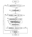
次に、図14のフローチャートを用いて寿命判定処理を説明していく。寿命判定処理を行うタイミングかどうかの判定(S1)においてイエスとされたとき、平均膜厚検出動作を実行する(S2)。次に、平均膜厚が下限値を下回っているかどうかを判断する(S3)。平均膜厚が下限値を下回っている場合には、感光体10の寿命が到来したと判断する(S8)。一方、平均膜厚が下限値を下回っていない場合、先述したように、減耗傾斜量検出用のトナーパッチの生成(S4)、減耗傾斜量検出用のトナーパッチの濃度と現像電流値の検出(S5)、減耗傾斜量の算出(S6)を行う。そして、前記減耗傾斜量が上限値を超えているかどうかを判断する(S7)。前記減耗傾斜量が上限値を超えている場合、感光体10の寿命が到来したと判断する(S8)。一方、前記減耗傾斜量が上限値を超えていない場合、前記ステップ3で寿命判定制御を終了する。なお、寿命判定制御を行うタイミングは、通常行われる安定化制御動作時とすることができる。
Next, the life determination process will be described with reference to the flowchart of FIG. When the result is yes in the determination (S1) of whether or not it is the timing to perform the life determination process, the average film thickness detection operation is executed (S2). Next, it is determined whether or not the average film thickness is below the lower limit value (S3). When the average film thickness is less than the lower limit value, it is determined that the life of the
次に、図15のフローチャートを用いて寿命予測処理を説明していく。寿命予測処理を行うタイミングかどうかの判定(S11)においてイエスとされたとき、平均膜厚検出動作を実行する(S12)。次に、現在の感光体回転数の情報を取得する処理(S13)、および平均膜厚の減少傾きを算出する処理(S14)を行う。これらの処理は、図5に示すような感光体回転数に対する平均膜厚推定値のプロットが示す傾斜の傾き算出に相当する。次に、平均膜厚の消耗率(%)を算出する(S15)。この平均膜厚の消耗率は、前記平均膜厚の減少傾きに現在の感光体回転数を乗算したもの(現時点の減少膜厚)を、初期膜厚と下限膜厚(寿命膜厚)との差で割って100を掛けたものである。 Next, the life prediction process will be described using the flowchart of FIG. When the result is yes in the determination (S11) of whether or not it is the timing to perform the life prediction process, the average film thickness detection operation is executed (S12). Next, a process of acquiring information on the current number of rotations of the photoconductor (S13) and a process of calculating the decrease slope of the average film thickness (S14) are performed. These processes correspond to the calculation of the slope of the inclination shown by the plot of the estimated average film thickness with respect to the number of rotations of the photoconductor as shown in FIG. Next, the consumption rate (%) of the average film thickness is calculated (S15). The consumption rate of this average film thickness is obtained by multiplying the decrease slope of the average film thickness by the current number of rotations of the photoconductor (current decrease film thickness) as the initial film thickness and the lower limit film thickness (lifetime film thickness). It is divided by the difference and multiplied by 100.
次に、先述したように、減耗傾斜量検出用のトナーパッチの生成(S16)、減耗傾斜量検出用のトナーパッチの濃度と現像電流値の検出(S17)、及び現在の感光体回転数と減耗傾斜量の算出を行う(S18)。そして、図6に示したような減耗傾斜量の増加傾きを算出し(S19)、この減耗傾斜量の増加率を算出する(S20)。この減耗傾斜量の増加率は、減耗傾斜量の増加傾きに現在の感光体回転数を乗算したもの(現時点の減耗傾斜量)を、減耗傾斜上限値(例えば、7μm)で割って100を掛けたものである。 Next, as described above, the generation of the toner patch for detecting the amount of depletion inclination (S16), the detection of the concentration and the developing current value of the toner patch for detecting the amount of depletion inclination (S17), and the current number of rotations of the photoconductor. The amount of depletion inclination is calculated (S18). Then, the increase slope of the depletion slope amount as shown in FIG. 6 is calculated (S19), and the increase rate of the depletion slope amount is calculated (S20). The rate of increase in the amount of depletion inclination is obtained by multiplying the increase inclination of the amount of depletion inclination by the current number of rotations of the photoconductor (current amount of depletion inclination), dividing by the upper limit value of depletion inclination (for example, 7 μm), and multiplying by 100. It is a thing.
次に、平均膜厚の消耗率と減耗傾斜量の増加率ではどちらの方が100%に近いかを判断する(S21)。平均膜厚の消耗率の方が100%に近い場合、この平均膜厚の消耗率を選択し(S22)、寿命予測を行う(S24)。一方、減耗傾斜量の増加率の方が100%に近い場合、減耗傾斜量の増加率を選択し(S23)、寿命予測を行う(S24)。前記寿命予測は、前記平均膜厚の消耗率や減耗傾斜量の増加率が100%に近いほど、寿命が近づいていると予測することになる。この寿命予測により、感光体10の寿命が実際に到来する前において減耗傾斜による画像不良の発生の回避ができるようになる。
Next, it is determined which is closer to 100% in terms of the consumption rate of the average film thickness and the increase rate of the amount of wear inclination (S21). When the consumption rate of the average film thickness is closer to 100%, the consumption rate of the average film thickness is selected (S22), and the life is predicted (S24). On the other hand, when the rate of increase in the amount of depletion inclination is closer to 100%, the rate of increase in the amount of depletion inclination is selected (S23) and the life is predicted (S24). The life prediction predicts that the closer the consumption rate of the average film thickness and the increase rate of the depletion slope amount are to 100%, the closer the life is. With this life prediction, it is possible to avoid the occurrence of image defects due to the wear inclination before the life of the
感光体10の膜厚傾斜のフィードバック先としては寿命予測ではなく、その膜厚傾斜を抑制(補正)する手段にフィードバックしても良い。
The feedback destination of the film thickness inclination of the
例えば、非画像印字時に感光体上に感光体膜厚に応じた膜厚抑制用のトナーパッチを生成する。この方法においては、感光体膜厚に応じて膜厚抑制用のトナーパッチの生成条件を変更してもよい。例えば、感光体膜厚の削れ量が大きい場所に現像剤が多く供給されるように、濃度を濃くしたパターンを供給するようにしてもよい。現像剤からの滑剤供給が不足すると、感光体10の摩擦係数が上がり、感光体膜厚の削れ量が大きくなるからである。一方、感光体膜厚の削れ量が小さい場所であれば、濃度を薄くしたパターンを供給するようにしてもよい。また、減耗傾斜量が多くなった場合に、膜厚修正用のトナーパッチの大きさを大きくしてもよい。例えば、感光体10の長手方向の広い範囲で傾斜していることが検知できた場合には長手方向のトナーパッチ幅を大きくする。また、極端に奥側のみ削れていないことが検知できた場合には幅は広げず、進行方向の長さを長くする。また、例えば、減耗傾斜量が多くなった場合に、それ以前においてA4プリント15枚に1回トナーパッチを作成していたのを、5枚に1回の頻度に生成条件を変更する。
For example, a toner patch for suppressing the film thickness according to the film thickness of the photoconductor is generated on the photoconductor during non-image printing. In this method, the conditions for generating the toner patch for suppressing the film thickness may be changed according to the film thickness of the photoconductor. For example, a pattern having a high density may be supplied so that a large amount of the developer is supplied to a place where the amount of scraping of the photoconductor film thickness is large. This is because if the lubricant supply from the developer is insufficient, the friction coefficient of the
また、膜厚傾斜を抑制する手段にフィードバックする手法としては、感光体表面に接触して清掃する清掃部材の押圧力を感光体膜厚の傾斜に応じて変更させてもよい。清掃部材の押圧力を感光体膜厚に応じて変化させる方法としては、清掃部材を移動させる機構を設け、感光体膜厚の傾斜に伴い、感光体への接触圧を変化させ感光体に当接させればよい。この時、清掃部材はクリーニングブレードの他に、ローラタイプなど別の清掃部材を新設してもよい。このようなフィードバックを行うことで、図16に示すように、感光体10の長手方向(回転軸方向)に生じる表面膜の傾斜を抑制することができた。
Further, as a method of feeding back to the means for suppressing the film thickness inclination, the pressing force of the cleaning member that comes into contact with the surface of the photoconductor for cleaning may be changed according to the inclination of the film thickness of the photoconductor. As a method of changing the pressing force of the cleaning member according to the film thickness of the photoconductor, a mechanism for moving the cleaning member is provided, and the contact pressure to the photoconductor is changed as the film thickness of the photoconductor is inclined to hit the photoconductor. You just have to touch it. At this time, in addition to the cleaning blade, another cleaning member such as a roller type may be newly installed as the cleaning member. By performing such feedback, as shown in FIG. 16, it was possible to suppress the inclination of the surface film that occurs in the longitudinal direction (rotational axis direction) of the
また、図13に示したように、前記画像形成装置100の膜厚推定部(寿命判定/予測)4において出力した像担持体(感光体であれば各色の感光体)の寿命判定や寿命予測を、通信部5を用いて前記管理装置1000に送信するようにしてもよい。或いは、前記画像形成装置100において寿命判定や寿命予測を行うのではなく、前記管理装置1000において前記画像形成装置100の像担持体(感光体であれば各色の感光体)の寿命判定や寿命予測を行うべく、前記像担持体上の一つのトナーパッチの濃度に基づく情報であって、前記像担持体の寿命判定或いは寿命予測に用いる情報、例えば、減耗傾斜量検出用のトナーパッチの濃度と現像電流値の検出値、現在の感光体等の回転数と減耗傾斜量の算出値、減耗傾斜量の増加傾きの算出値、減耗傾斜量の増加率等を、前記管理装置1000に送信してもよい。もちろん、前記一つのトナーパッチに基づく情報以外の情報である前記平均膜厚の消耗等に関する情報を送信するようにしてもよい。
Further, as shown in FIG. 13, the life determination and the life prediction of the image carrier (photoreceptor of each color if it is a photoconductor) output by the film thickness estimation unit (lifetime determination / prediction) 4 of the
前記管理装置1000においては、管理対象となる画像形成装置の像担持体の寿命判定或いは寿命予測に基づいて、当該像担持体の交換時期を管理する。前記管理装置1000は例えばサービスセンターに設けられており、サービスマンに各画像形成装置の像担持体の交換時期を知らせる。これにより、サービスマンの顧客訪問を効率良く行うことが可能となり、サービスやメンテナンスにかかるコストを低減することが可能となる。
The
また、以上の例では、検出した現像電流に基づいて像担持体の膜厚差推定を行ったが、前記転写電流検出部3により転写時に検出される転写電流値に基づいて像担持体の膜厚差推定を行うことができる。
Further, in the above example, the film thickness difference of the image carrier was estimated based on the detected development current, but the film of the image carrier was estimated based on the transfer current value detected by the transfer
1 :IDCセンサー
2 :現像電流検出部
3 :転写電流検出部
4 :膜厚差推定部
5 :通信部
10 :感光体(像担持体)
11 :帯電装置
12 :潜像形成装置
13 :現像装置
14 :中間転写ベルト
14a :回転ローラー
15 :一次転写ローラー(第二像担持体)
16 :二次転写ローラー
18 :タイミングローラー
19 :定着装置
20 :排紙ローラー
30 :第1のクリーニング装置
31 :第2のクリーニング装置
41 :給紙ローラー
100 :画像形成装置
1000 :管理装置
S :用紙
1: IDC sensor 2: Development current detection unit 3: Transfer current detection unit 4: Film thickness difference estimation unit 5: Communication unit 10: Photoreceptor (image carrier)
11: Charging device 12: Latent image forming device 13: Developing device 14:
16: Secondary transfer roller 18: Timing roller 19: Fixing device 20: Paper ejection roller 30: First cleaning device 31: Second cleaning device 41: Paper feed roller 100: Image forming device 1000: Management device S: Paper
Claims (10)
前記像担持体上の前記回転移動の回転軸方向の異なる2以上の位置に前記現像剤のトナーを用いて2以上のトナーパッチを付与し、前記トナーパッチのうち一つのトナーパッチの濃度を検出し、前記一つのトナーパッチの濃度を用いて前記像担持体の表面膜における前記回転軸方向の膜厚差を推定することを特徴とする膜厚差推定方法。 The film thickness difference estimation method performed by the image forming apparatus according to any one of claims 1 to 8.
Two or more toner patches are applied to two or more positions on the image carrier in different rotation axis directions of the rotational movement using the toner of the developer, and the concentration of one of the toner patches is detected. A method for estimating a film thickness difference, which comprises estimating the film thickness difference in the rotation axis direction of the surface film of the image carrier using the concentration of the one toner patch.
前記画像形成装置は、前記管理装置が当該画像形成装置の像担持体の交換時期を管理するための情報として、少なくとも前記一つのトナーパッチの濃度に基づく情報であって、前記像担持体の寿命判定或いは寿命予測に用いる情報を前記管理装置に送信することを特徴とする管理システム。 A management system in which the image forming apparatus according to any one of claims 1 to 8 is communicably connected to the management apparatus.
The image forming apparatus is information based on the concentration of at least one toner patch as information for the management apparatus to manage the replacement timing of the image carrier of the image forming apparatus, and is the life of the image bearing. A management system characterized in that information used for determination or life prediction is transmitted to the management device.
Priority Applications (1)
| Application Number | Priority Date | Filing Date | Title |
|---|---|---|---|
| JP2017050993A JP6926552B2 (en) | 2017-03-16 | 2017-03-16 | Image forming device, film thickness difference estimation method and management system |
Applications Claiming Priority (1)
| Application Number | Priority Date | Filing Date | Title |
|---|---|---|---|
| JP2017050993A JP6926552B2 (en) | 2017-03-16 | 2017-03-16 | Image forming device, film thickness difference estimation method and management system |
Publications (2)
| Publication Number | Publication Date |
|---|---|
| JP2018155837A JP2018155837A (en) | 2018-10-04 |
| JP6926552B2 true JP6926552B2 (en) | 2021-08-25 |
Family
ID=63716429
Family Applications (1)
| Application Number | Title | Priority Date | Filing Date |
|---|---|---|---|
| JP2017050993A Active JP6926552B2 (en) | 2017-03-16 | 2017-03-16 | Image forming device, film thickness difference estimation method and management system |
Country Status (1)
| Country | Link |
|---|---|
| JP (1) | JP6926552B2 (en) |
Families Citing this family (11)
| Publication number | Priority date | Publication date | Assignee | Title |
|---|---|---|---|---|
| JP7216890B2 (en) * | 2019-01-28 | 2023-02-02 | 京セラドキュメントソリューションズ株式会社 | image forming device |
| JP7177984B2 (en) * | 2019-01-28 | 2022-11-25 | 京セラドキュメントソリューションズ株式会社 | image forming device |
| JP7216891B2 (en) * | 2019-01-28 | 2023-02-02 | 京セラドキュメントソリューションズ株式会社 | image forming device |
| JP7283115B2 (en) * | 2019-02-21 | 2023-05-30 | 京セラドキュメントソリューションズ株式会社 | Image forming apparatus and image forming method |
| JP2020149004A (en) * | 2019-03-15 | 2020-09-17 | 株式会社リコー | Image forming device |
| JP7215263B2 (en) * | 2019-03-18 | 2023-01-31 | コニカミノルタ株式会社 | image forming device |
| JP2021131480A (en) * | 2020-02-20 | 2021-09-09 | 京セラドキュメントソリューションズ株式会社 | Image forming device |
| JP7459601B2 (en) * | 2020-03-25 | 2024-04-02 | 京セラドキュメントソリューションズ株式会社 | Image forming device |
| JP7415722B2 (en) * | 2020-03-25 | 2024-01-17 | 京セラドキュメントソリューションズ株式会社 | Image forming device |
| JP7409200B2 (en) * | 2020-04-01 | 2024-01-09 | 京セラドキュメントソリューションズ株式会社 | Image forming device |
| JP7739972B2 (en) * | 2021-11-24 | 2025-09-17 | コニカミノルタ株式会社 | Image forming apparatus, control method for image forming apparatus, and control program for image forming apparatus |
Family Cites Families (8)
| Publication number | Priority date | Publication date | Assignee | Title |
|---|---|---|---|---|
| JP2006064955A (en) * | 2004-08-26 | 2006-03-09 | Ricoh Co Ltd | Image forming apparatus |
| JP2006235023A (en) * | 2005-02-23 | 2006-09-07 | Konica Minolta Business Technologies Inc | Image forming apparatus |
| JP4732261B2 (en) * | 2006-07-21 | 2011-07-27 | シャープ株式会社 | Image forming apparatus |
| JP2010107727A (en) * | 2008-10-30 | 2010-05-13 | Konica Minolta Business Technologies Inc | Image forming apparatus |
| JP5375456B2 (en) * | 2009-09-03 | 2013-12-25 | コニカミノルタ株式会社 | Image forming apparatus |
| JP2015166820A (en) * | 2014-03-04 | 2015-09-24 | コニカミノルタ株式会社 | image forming apparatus |
| JP6365094B2 (en) * | 2014-08-07 | 2018-08-01 | 富士ゼロックス株式会社 | Information processing apparatus and life management system |
| JP2017009876A (en) * | 2015-06-24 | 2017-01-12 | 株式会社リコー | Latent image carrier evaluation apparatus, image forming apparatus, and latent image carrier evaluation method |
-
2017
- 2017-03-16 JP JP2017050993A patent/JP6926552B2/en active Active
Also Published As
| Publication number | Publication date |
|---|---|
| JP2018155837A (en) | 2018-10-04 |
Similar Documents
| Publication | Publication Date | Title |
|---|---|---|
| JP6926552B2 (en) | Image forming device, film thickness difference estimation method and management system | |
| JP5630708B2 (en) | Image forming apparatus | |
| JP5169702B2 (en) | Image forming method and image forming apparatus | |
| JP2006039036A (en) | Method and device for estimating toner concentration, and image forming apparatus equipped with device | |
| JP7389964B2 (en) | Image forming device | |
| JP4946061B2 (en) | Image forming apparatus | |
| US10061250B2 (en) | Image forming apparatus and photoconductor evaluation method | |
| JP2011028202A (en) | Image forming apparatus | |
| JP6432061B2 (en) | Image forming apparatus | |
| JP2018005073A (en) | Image formation device | |
| JP4722648B2 (en) | Image forming apparatus | |
| JP2014016559A (en) | Image forming apparatus | |
| JP6145800B2 (en) | Image forming apparatus | |
| JP7254510B2 (en) | image forming device | |
| JP2017223841A (en) | Toner forced consumption method and image forming apparatus | |
| US11106152B2 (en) | Image forming apparatus | |
| JP2005331720A (en) | Image forming apparatus | |
| JP5605074B2 (en) | Image forming apparatus | |
| JP2002082578A (en) | Image forming method and image forming device | |
| JP4948100B2 (en) | Toner consumption prediction amount calculation method, toner consumption prediction amount calculation device, and image forming apparatus | |
| JP5127373B2 (en) | Image forming apparatus | |
| JP2012108196A (en) | Image forming apparatus and maintenance management system of image forming apparatus | |
| JP2018189787A (en) | Image formation device, and carrier state judgement method | |
| JP2014149487A (en) | Image forming apparatus | |
| US11385585B2 (en) | Determination of remaining life of photoconductor |
Legal Events
| Date | Code | Title | Description |
|---|---|---|---|
| A621 | Written request for application examination |
Free format text: JAPANESE INTERMEDIATE CODE: A621 Effective date: 20200214 |
|
| A977 | Report on retrieval |
Free format text: JAPANESE INTERMEDIATE CODE: A971007 Effective date: 20201221 |
|
| A131 | Notification of reasons for refusal |
Free format text: JAPANESE INTERMEDIATE CODE: A131 Effective date: 20210202 |
|
| A521 | Written amendment |
Free format text: JAPANESE INTERMEDIATE CODE: A523 Effective date: 20210331 |
|
| TRDD | Decision of grant or rejection written | ||
| A01 | Written decision to grant a patent or to grant a registration (utility model) |
Free format text: JAPANESE INTERMEDIATE CODE: A01 Effective date: 20210706 |
|
| A61 | First payment of annual fees (during grant procedure) |
Free format text: JAPANESE INTERMEDIATE CODE: A61 Effective date: 20210719 |
|
| R150 | Certificate of patent or registration of utility model |
Ref document number: 6926552 Country of ref document: JP Free format text: JAPANESE INTERMEDIATE CODE: R150 |