JP6738224B2 - LED package - Google Patents
LED package Download PDFInfo
- Publication number
- JP6738224B2 JP6738224B2 JP2016142006A JP2016142006A JP6738224B2 JP 6738224 B2 JP6738224 B2 JP 6738224B2 JP 2016142006 A JP2016142006 A JP 2016142006A JP 2016142006 A JP2016142006 A JP 2016142006A JP 6738224 B2 JP6738224 B2 JP 6738224B2
- Authority
- JP
- Japan
- Prior art keywords
- led package
- package according
- led
- case
- present
- Prior art date
- Legal status (The legal status is an assumption and is not a legal conclusion. Google has not performed a legal analysis and makes no representation as to the accuracy of the status listed.)
- Active
Links
Images


Classifications
-
- H—ELECTRICITY
- H01—ELECTRIC ELEMENTS
- H01L—SEMICONDUCTOR DEVICES NOT COVERED BY CLASS H10
- H01L2224/00—Indexing scheme for arrangements for connecting or disconnecting semiconductor or solid-state bodies and methods related thereto as covered by H01L24/00
- H01L2224/01—Means for bonding being attached to, or being formed on, the surface to be connected, e.g. chip-to-package, die-attach, "first-level" interconnects; Manufacturing methods related thereto
- H01L2224/42—Wire connectors; Manufacturing methods related thereto
- H01L2224/47—Structure, shape, material or disposition of the wire connectors after the connecting process
- H01L2224/48—Structure, shape, material or disposition of the wire connectors after the connecting process of an individual wire connector
- H01L2224/4805—Shape
- H01L2224/4809—Loop shape
- H01L2224/48091—Arched
-
- H—ELECTRICITY
- H01—ELECTRIC ELEMENTS
- H01L—SEMICONDUCTOR DEVICES NOT COVERED BY CLASS H10
- H01L2224/00—Indexing scheme for arrangements for connecting or disconnecting semiconductor or solid-state bodies and methods related thereto as covered by H01L24/00
- H01L2224/73—Means for bonding being of different types provided for in two or more of groups H01L2224/10, H01L2224/18, H01L2224/26, H01L2224/34, H01L2224/42, H01L2224/50, H01L2224/63, H01L2224/71
- H01L2224/732—Location after the connecting process
- H01L2224/73251—Location after the connecting process on different surfaces
- H01L2224/73265—Layer and wire connectors
-
- H—ELECTRICITY
- H01—ELECTRIC ELEMENTS
- H01L—SEMICONDUCTOR DEVICES NOT COVERED BY CLASS H10
- H01L2924/00—Indexing scheme for arrangements or methods for connecting or disconnecting semiconductor or solid-state bodies as covered by H01L24/00
- H01L2924/15—Details of package parts other than the semiconductor or other solid state devices to be connected
- H01L2924/181—Encapsulation
Description
本発明は、リモートセンサや各種照明器具などに用いられるLEDパッケージに関する。 The present invention relates to an LED package used for remote sensors, various lighting fixtures, and the like.
LEDパッケージの形態として、導電部が形成された基板にLED素子を搭載し、LED素子を囲むケースを基板に配置し、基板およびケースにより形成される凹部に封止樹脂を充填させた形態が、従来から広く知られている。ケースの内面は、LED素子から発せられた光を反射するリフレクタとしての機能を果たしている。ケースを備えることによって、LED素子から発せられる光の取り出し効率の向上が図られる。 As a form of the LED package, an LED element is mounted on a substrate on which a conductive portion is formed, a case surrounding the LED element is arranged on the substrate, and a recess formed by the substrate and the case is filled with a sealing resin. It has been widely known from the past. The inner surface of the case functions as a reflector that reflects the light emitted from the LED element. By providing the case, the extraction efficiency of the light emitted from the LED element can be improved.
一方、当該LEDパッケージにおいて、封止樹脂と空気との界面(開口面)に光が入射するとき、界面を境界として絶対屈折率が異なることから、光の入射角がスネルの法則によって定義される臨界角を超える角度であれば、光は当該界面で反射することとなる。このような反射が繰り返されると、光の経路が長くなるにつれて封止樹脂に光が吸収され、LED素子から発せられる光の取り出し効率が逆に低下するおそれがある。 On the other hand, in the LED package, when light is incident on the interface (opening surface) between the encapsulating resin and air, the absolute refractive index is different at the interface, so the incident angle of light is defined by Snell's law. If the angle exceeds the critical angle, light will be reflected at the interface. When such reflection is repeated, light may be absorbed by the sealing resin as the light path becomes longer, and conversely, the extraction efficiency of light emitted from the LED element may decrease.
こうした課題を解決するために、たとえば特許文献1には、光の出射方向に突出した凸型のレンズを備えることによって、LED素子から発せられた光を集光し、光の取り出し効率が高くなるようにしたLEDパッケージが開示されている。また、特許文献2には、ケース内に充填された封止樹脂の形状を、光の出射方向に突出した凸型とすることで、特許文献1に開示されているLEDパッケージと同様な効果が得られるLEDパッケージが開示されている。ただし、特許文献1および2に開示されているLEDパッケージは、ともに凸型の突出部が形成されているため、LEDパッケージの低背化や小型化が困難になるという問題がある。
In order to solve such a problem, for example, in
本発明は上記事情に鑑み、低背化や小型化を図りつつ、光の取り出し効率を高くすることが可能なLEDパッケージを提供することをその課題とする。 In view of the above circumstances, it is an object of the present invention to provide an LED package capable of increasing the light extraction efficiency while achieving a low profile and a small size.
本発明によって提供されるLEDパッケージは、LED素子と、互いに反対側を向く主面および実装面を有する基板と、前記主面と同一方向を向くとともに前記LED素子を搭載する搭載面を有し、かつ前記主面および前記実装面の双方に形成された導電部と、互いに反対側を向く端面および支持面と、前記端面および前記支持面につながるとともに前記LED素子を囲むように形成された反射面と、を有し、かつ前記支持面が前記主面に向くように配置されたケースと、互いに反対側を向く頂面および裏面を有し、かつ前記裏面が前記端面を向くように前記ケースを覆う透光性がある蓋と、を備え、前記頂面は平たんであり、前記蓋には、前記裏面から前記LED素子に向かって突出した凸型のレンズ部が形成され、前記レンズ部が、前記端面、前記支持面および前記反射面によって前記ケースに形成された貫通領域に収容されていることを特徴としている。 An LED package provided by the present invention has an LED element, a substrate having a main surface and a mounting surface facing opposite sides, and a mounting surface facing the same direction as the main surface and mounting the LED element, Also, conductive portions formed on both the main surface and the mounting surface, end surfaces and supporting surfaces facing opposite sides, and a reflecting surface connected to the end surfaces and the supporting surface and surrounding the LED element. And a case arranged so that the support surface faces the main surface, and a top surface and a back surface facing opposite sides, and the case so that the back surface faces the end surface. A cover having a translucent property, the top surface is flat, and a convex lens portion protruding from the back surface toward the LED element is formed on the lid, and the lens portion is The end surface, the support surface, and the reflection surface are housed in a penetrating region formed in the case.
本発明の実施において好ましくは、前記蓋は、合成樹脂からなる。 In the practice of the present invention, preferably, the lid is made of synthetic resin.
本発明の実施において好ましくは、前記蓋は、ガラスからなる。 In the practice of the present invention, preferably, the lid is made of glass.
本発明の実施において好ましくは、前記LED素子は、透光性がある封止樹脂によって覆われている。 In the practice of the present invention, preferably, the LED element is covered with a translucent sealing resin.
本発明の実施において好ましくは、前記封止樹脂は、蛍光体が含有された合成樹脂からなる。 In the practice of the present invention, preferably, the sealing resin is made of a synthetic resin containing a phosphor.
本発明の実施において好ましくは、前記封止樹脂は、シリコーン樹脂を含む。 In the practice of the present invention, preferably, the sealing resin contains a silicone resin.
本発明の実施において好ましくは、前記貫通領域の一部が前記封止樹脂により充填されている。 In the practice of the present invention, preferably, a part of the penetrating region is filled with the sealing resin.
本発明の実施において好ましくは、前記封止樹脂の形状は、凸型である。 In the practice of the present invention, preferably, the shape of the sealing resin is convex.
本発明の実施において好ましくは、前記貫通領域の全部が前記封止樹脂により充填されている。 In the practice of the present invention, preferably, the entire penetrating region is filled with the sealing resin.
本発明の実施において好ましくは、前記基板には、前記主面から前記実装面に至って貫通し、かつ外部の空気が流通する通気孔が形成され、前記通気孔は、前記貫通領域に通じている。 In the practice of the present invention, preferably, the substrate is formed with a vent hole penetrating from the main surface to the mounting surface and through which external air flows, and the vent hole communicates with the penetrating region. ..
本発明の実施において好ましくは、前記反射面は、白色である。 In the practice of the invention, preferably, the reflective surface is white.
本発明の実施において好ましくは、前記ケースには、前記反射面を覆う鏡面めっき層が形成されている。 In the practice of the present invention, preferably, the case is formed with a mirror plating layer covering the reflection surface.
本発明の実施において好ましくは、前記鏡面めっき層は、Auを含む。 In the practice of the present invention, preferably, the specular plating layer contains Au.
本発明の実施において好ましくは、前記導電部は、互いに積層されためっき層を含む。 In the practice of the present invention, preferably, the conductive portion includes plating layers stacked on each other.
本発明の実施において好ましくは、前記めっき層は、Auを含む。 In the practice of the present invention, preferably, the plating layer contains Au.
本発明の実施において好ましくは、前記基板の内部に形成された連絡導電部をさらに備え、前記連絡導電部が前記主面および前記実装面からともに露出している。 In implementation of the present invention, preferably, a communication conductive portion formed inside the substrate is further provided, and the communication conductive portion is exposed from both the main surface and the mounting surface.
本発明の実施において好ましくは、前記連絡導電部の形状は、円柱状である。 In the practice of the present invention, preferably, the shape of the connecting conductive portion is a column shape.
本発明の実施において好ましくは、前記貫通領域の平面視形状は、円形状である。 In implementation of the present invention, preferably, the shape of the penetrating region in plan view is circular.
本発明の実施において好ましくは、前記反射面は、前記支持面に対して傾斜している。 In the practice of the present invention, preferably, the reflecting surface is inclined with respect to the supporting surface.
本発明の実施において好ましくは、前記反射面は、前記支持面から起立している第1反射面と、前記端面および前記第1反射面につながり、かつ前記支持面に対して傾斜している第2反射面とを含み、前記第1反射面と前記第2反射面とが交差する境界部の平面視形状は、円形状である。 In the practice of the invention, preferably, the reflecting surface is connected to the first reflecting surface standing upright from the supporting surface, the end surface and the first reflecting surface, and is inclined with respect to the supporting surface. A two-reflecting surface is included, and a boundary portion where the first reflecting surface and the second reflecting surface intersect each other has a circular shape in a plan view.
本発明の実施において好ましくは、前記LED素子は、発光部が形成された素子主面を有し、前記基板の厚さ方向において、前記素子主面は前記境界部と前記基板の前記主面との間に位置している。 In the practice of the present invention, preferably, the LED element has an element main surface on which a light emitting portion is formed, and in the thickness direction of the substrate, the element main surface is the boundary portion and the main surface of the substrate. It is located between
本発明の実施において好ましくは、前記主面から窪む開口部が形成され、前記開口部から前記導電部の前記搭載面が露出している。 In implementation of the present invention, preferably, an opening is formed that is recessed from the main surface, and the mounting surface of the conductive portion is exposed from the opening.
本発明の実施において好ましくは、前記基板の前記開口部は、前記主面から前記実装面に至って貫通し、前記導電部は、一部が前記実装面から前記開口部を塞ぎ、他の部分が前記実装面に接する金属箔を含む。 In the practice of the present invention, preferably, the opening of the substrate penetrates from the main surface to the mounting surface, and the conductive portion partially closes the opening from the mounting surface, and the other portion is A metal foil in contact with the mounting surface is included.
本発明の実施において好ましくは、前記金属箔は、前記めっき層によって覆われている。 In the practice of the present invention, preferably, the metal foil is covered with the plating layer.
本発明の実施において好ましくは、前記金属箔は、Cuからなる。 In the practice of the present invention, preferably, the metal foil is made of Cu.
本発明の実施において好ましくは、前記LED素子と前記搭載面との間に介在する導電体である接合層を備える。 In practicing the present invention, preferably, a bonding layer, which is a conductor, is provided between the LED element and the mounting surface.
本発明の実施において好ましくは、前記LED素子と前記導電部とを接続するボンディングワイヤを備える。 In practicing the present invention, preferably, a bonding wire connecting the LED element and the conductive portion is provided.
本発明の実施において好ましくは、前記ケースは、前記支持面から前記端面に向かって窪み、かつ一端が前記反射面につながる中間面と、前記中間面および前記支持面を相互につなぐ内側面と、を有し、前記ボンディングワイヤの一部が、前記中間面、前記内側面および前記支持面によって前記ケースに形成された凹部に収容されている。 In the practice of the present invention, preferably, the case is recessed from the support surface toward the end surface, and an intermediate surface having one end connected to the reflective surface, and an inner surface connecting the intermediate surface and the support surface to each other, And a part of the bonding wire is housed in a recess formed in the case by the intermediate surface, the inner surface, and the support surface.
本発明の実施において好ましくは、前記ケースには、前記貫通領域と前記凹部との間に介在し、かつ前記中間面と、前記中間面につながる前記反射面との各々一部ずつが除去された切欠部が形成され、前記ボンディングワイヤが、前記切欠部を通過している。 In the practice of the invention, preferably, in the case, a part of each of the intermediate surface and the reflective surface connected to the intermediate surface, which is interposed between the penetrating region and the recess, is removed. A cutout is formed, and the bonding wire passes through the cutout.
本発明の実施において好ましくは、前記導電部の前記搭載面に搭載され、かつ前記凹部に収容されたツェナーダイオードを備える。 In implementing the present invention, preferably, a Zener diode mounted on the mounting surface of the conductive portion and housed in the recess is provided.
本発明の実施において好ましくは、前記蓋には、各々が前記蓋の前記頂面に対して傾斜する第1傾斜面および前記第2傾斜面を有するとともに、平面視において一方向に延出し、かつ前記貫通領域の一部が重なるプリズム部が形成され、前記第1傾斜面および前記第2傾斜面は、各々の一端が前記頂面につながり、かつ各々の他端が相互につながり、前記頂面と前記第1傾斜面とがなす鋭角は、前記頂面と前記第2傾斜面とがなす鋭角よりも小である。 In implementation of the present invention, preferably, the lid has a first inclined surface and a second inclined surface that are inclined with respect to the top surface of the lid, and extends in one direction in a plan view, and A prism portion is formed in which a part of the penetrating region overlaps, one end of each of the first inclined surface and the second inclined surface is connected to the top surface, and each other end of the first inclined surface and the second inclined surface is connected to each other. The acute angle formed by the first inclined surface and the first inclined surface is smaller than the acute angle formed by the top surface and the second inclined surface.
本発明の実施において好ましくは、前記蓋の前記頂面は、前記プリズム部と同方向に延出する中央頂面を含み、前記中央頂面が延出する方向と直角である方向における前記中央頂面の両端に、前記プリズム部の各々が位置し、かつ各々の前記プリズム部の第1傾斜面がつながり、平面視において前記LED素子の一部が前記中央頂面に重なる。 In the practice of the present invention, preferably, the top surface of the lid includes a central top surface extending in the same direction as the prism portion, and the central top surface in a direction perpendicular to the extending direction of the central top surface. Each of the prism portions is located at both ends of the surface, and the first inclined surfaces of the prism portions are connected to each other, and a part of the LED element overlaps with the central top surface in a plan view.
本発明によれば、LEDパッケージの基板に配置されたケースは、互いに反対側を向く端面および支持面と、端面および支持面につながるとともにLED素子を囲むように形成された反射面とを有する。また、ケースを覆うように配置された蓋には、裏面からLED素子に向かって突出したレンズ部が形成されている。そして、当該レンズ部が、端面、支持面および反射面によってケースに形成された貫通領域内に収容されている。このような構成をとることによって、当該レンズ部がLED素子から発せられた光を集光させるため、光の取り出し効率を高くすることができる。また、レンズ部が貫通領域内に収容されることから、LEDパッケージの低背化や小型化を図ることができる。したがって、LEDパッケージの低背化や小型化を図りつつ、光の取り出し効率を高くすることが可能となる。 According to the present invention, the case arranged on the substrate of the LED package has an end surface and a supporting surface facing opposite sides, and a reflecting surface connected to the end surface and the supporting surface and surrounding the LED element. Further, a lens portion protruding from the back surface toward the LED element is formed on the lid arranged so as to cover the case. Then, the lens portion is housed in a penetrating region formed in the case by the end surface, the supporting surface, and the reflecting surface. With such a configuration, the lens unit condenses the light emitted from the LED element, so that the light extraction efficiency can be increased. Further, since the lens portion is housed in the penetrating region, it is possible to reduce the height and size of the LED package. Therefore, it is possible to increase the light extraction efficiency while reducing the height and size of the LED package.
本発明のその他の特徴および利点は、添付図面に基づき以下に行う詳細な説明によって、より明らかとなろう。 Other features and advantages of the present invention will become more apparent from the detailed description given below with reference to the accompanying drawings.
本発明を実施するための形態(以下「実施形態」という。)について、添付図面に基づいて説明する。 Modes for carrying out the present invention (hereinafter referred to as "embodiments") will be described with reference to the accompanying drawings.
〔第1実施形態〕
図1〜図5に基づき、本発明の第1実施形態にかかるLEDパッケージA10について説明する。これらの図に示すLEDパッケージA10は、たとえばリモートセンサの回路基板に表面実装されるものである。本実施形態にかかるLEDパッケージA10は、基板1、導電部21、連絡導電部22、LED素子31、接合層32、ケース4、蓋5およびボンディングワイヤ6を備える。LEDパッケージA10は、平面視矩形状である。
[First Embodiment]
The LED package A10 according to the first embodiment of the present invention will be described with reference to FIGS. The LED package A10 shown in these figures is surface-mounted on a circuit board of a remote sensor, for example. The LED package A10 according to this embodiment includes a
図1は、LEDパッケージA10の平面図であり、理解の便宜上、蓋5を省略している。図2は、LEDパッケージA10の底面図である。図3は、図1のIII−III線に沿う断面図である。図4は、図1のIV−IV線に沿う断面図である。図5は、LEDパッケージA10の蓋5の斜視図である。なお、図3および図4においては、蓋5を省略せずに図示している。
FIG. 1 is a plan view of the LED package A10, and the
基板1は、LED素子31およびケース4を支持し、かつLEDパッケージA10を回路基板に実装するためのものである。基板1は、電気絶縁体である。たとえばアルミナ(Al2O3)などのセラミックス、またはガラスエポキシ樹脂からなる。LEDパッケージA10の使用時に、LED素子31より発生した熱を外部に放出しやすくするため、基板1は熱伝導率が比較的高い材料であることが好ましい。本実施形態においては、基板1は、主面11、実装面12および複数の基板側面13を有する。
The
主面11は、図3および図4に示す基板1の上面である。LEDパッケージA10において、主面11が向く方向にLED素子31が位置している。実装面12は、図3および図4に示す基板1の下面である。実装面12は、LEDパッケージA10を対象となる回路基板に実装する際に利用される面である。図3および図4に示すように、主面11および実装面12は、ともに基板1の厚さ方向に対して直交し、かつ平たんである。また、主面11および実装面12は、基板1の厚さ方向において互いに反対側を向いている。
The
図3および図4に示すように、複数の基板側面13は、基板1の厚さ方向において主面11と実装面12との間に挟まれ、かつLEDパッケージA10の外側を向く4つの面である。複数の基板側面13は、いずれも主面11および実装面12に直交し、かつ平たんである。
As shown in FIGS. 3 and 4, the plurality of substrate side surfaces 13 are four surfaces which are sandwiched between the
図1〜図3に示すように、基板1には、主面11から実装面12に至って貫通し、かつLEDパッケージA10の外部の空気が流通する通気孔15が形成されている。通気孔15は、後述するケース4に形成された貫通領域46に通じている。通気孔15は、本実施形態のように基板1に設けた貫通孔に替えて、後述するケース4の支持面42から窪み、かつ外部と貫通領域46とを相互に空気が流通する貫通溝であってもよい。
As shown in FIGS. 1 to 3, the
導電部21は、LED素子31と対象となる回路基板との導電経路の一部を構成する、主面11および実装面12の双方に形成された部材である。本実施形態においては、主面11に形成された導電部21は、接合層32およびボンディングワイヤ6を介してLED素子31に導通している。本実施形態においては、導電部21は、搭載面211を有し、かつめっき層212を含む。図1および図2に示すように、主面11および実装面12の各々において、搭載面211は、互いに離間して形成されている。なお、主面11に形成された導電部21は、ともに基板側面13に接して形成されている。
The
図1、図3および図4に示すように、搭載面211は主面11と同一方向を向く、めっき層212の表面の一部である。搭載面211にLED素子31がダイボンディングによって搭載されている。めっき層212は、互いに積層された金属層からなる。本実施形態においては、めっき層212は電解めっきにより形成され、主面11、または実装面12から外側に向かってCu層、Ni層およびAu層の順に積層されている。
As shown in FIGS. 1, 3 and 4, the mounting
連絡導電部22は、図2および図3に示すように、主面11に形成された導電部21と、実装面12に形成された導電部21とを互いに導通させるための導電経路となる部材である。連絡導電部22は、基板1の内部に埋め込まれた状態となるように形成され、連絡導電部22が主面11および実装面12からともに露出している。主面11および実装面12から露出した連絡導電部22は、ともに導電部21に覆われている。本実施形態においては、連絡導電部22の形状は円柱状である。連絡導電部22は、たとえばCuからなる。
As shown in FIGS. 2 and 3, the connecting
なお、図1〜図4に示す導電部21および連絡導電部22の配置形態は一例であり、実際のLEDパッケージA10における導電部21および連絡導電部22の配置形態は、これに限定されない。
The arrangement of the
LED素子31は、LEDパッケージA10の光源となる発光素子であるとともに、たとえばpn接合により複数の半導体層が互いに積層された半導体素子である。LEDパッケージA10に電流が流れるとLED素子31が発光する。前記半導体層を構成する物質により、LED素子31は青色光、赤色光または緑色光などを発する。本実施形態においては、図3および図4に示すLED素子31の上面である素子主面311にp側電極(アノード)が、図3および図4に示すLED素子31の下面である素子裏面312にn側電極(カソード)が形成されている。また、LED素子31の発光部が、当該p側電極とともに素子主面311に形成されている。当該p側電極にボンディングワイヤ6が接続され、当該n側電極は接合層32を介して主面11に形成された導電部21に導通している。
The
接合層32は、図3および図4に示すように、LED素子31と搭載面211との間に介在する導電体である。接合層32によって固着されることで、搭載面211にLED素子31が搭載される。また、接合層32は導電体であることから、接合層32は導電部21および連絡導電部22とともに、LED素子31と対象となる回路基板との導電経路の一部を構成する。接合層32は、たとえばAgペーストからなる。
As shown in FIGS. 3 and 4, the
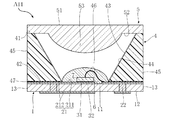
ケース4は、LED素子31を囲むように、主面11に配置された部材である。ケース4は、LED素子31から発せられた光を反射するリフレクタとしての機能を果たす。ケース4は、たとえばエポキシ樹脂やPPA(ポリフタルアミド)からなり、かつ電気絶縁体である。本実施形態においては、ケース4は、端面41、支持面42、反射面43、鏡面めっき層44、複数のケース側面45、貫通領域46および接着層47を有する。
The
端面41は、図3および図4に示すケース4の上面である。支持面42は、図3および図4に示すケース4の下面である。図3および図4に示すように、端面41および支持面42は、ともにケース4の厚さ方向に対して直交し、かつ平たんである。また、端面41および支持面42は、ケース4の厚さ方向において互いに反対側を向いている。ケース4は、支持面42が主面11に向くように配置されている。
The
図1、図3および図4に示すように、反射面43は、端面41および支持面42につながるとともに、LED素子31を囲むように形成された曲面である。本実施形態においては、反射面43は、支持面42に対して一定の角度で傾斜している。したがって、ケース4において、端面41の面積よりも支持面42の面積の方が大である。
As shown in FIGS. 1, 3 and 4, the
図3および図4に示すように、鏡面めっき層44は、反射面43を覆うように形成された金属層である。鏡面めっき層44は、無電解めっきにより形成される。本実施形態においては、鏡面めっき層44は、Au層、Ag層、Zn層およびAuとCoとの合金層のいずれかを選択することができる。なお、ケース4においては、鏡面めっき層44を省略し、白色に着色された反射面43が露出された状態であってもよい。
As shown in FIGS. 3 and 4, the mirror-plated
図3および図4に示すように、複数のケース側面45は、ケース4の厚さ方向において端面41と支持面42との間に挟まれ、かつLEDパッケージA10の外側を向く4つの面である。複数のケース側面45は、いずれも主面11および実装面12に直交し、かつ平たんである。また、複数のケース側面45と複数の基板側面13とは、いずれの面においても面一となっている。
As shown in FIGS. 3 and 4, the plurality of case side surfaces 45 are four surfaces which are sandwiched between the
図1、図3および図4に示すように、貫通領域46は、端面41、支持面42および反射面43によりケース4に形成された中空領域である。端面41および支持面42の双方に対して平行に沿った貫通領域46の断面積は、端面41と反射面43との境界において最も大となっている。本実施形態においては、貫通領域46の形状は、端面41に沿った上底の面積が、支持面42に沿った下底の面積よりも大とされる円錐台である。これにより、貫通領域46の平面視形状は円形状である。また、本実施形態においては、貫通領域46にLED素子31の一部が収容されている。
As shown in FIGS. 1, 3 and 4, the penetrating
図3および図4に示すように、接着層47は、支持面42と主面11との間に、または支持面42と導電部21との間に介在する部材である。接着層47によって固着されることで、基板1にケース4が配置される。本実施形態においては、接着層47は、たとえば紫外線硬化性があるアクリル樹脂またはエポキシ樹脂からなる。
As shown in FIGS. 3 and 4, the
蓋5は、ケース4を覆う透光性がある部材である。蓋5は、頂面51、裏面52およびレンズ部53を有する。頂面51は、図3および図4に示す蓋5の上面である。裏面52は、図3および図4に示す蓋5の下面である。図3〜図5に示すように、頂面51および裏面52は、ともに蓋5の厚さ方向に対して直交し、かつ平たんである。また、頂面51および裏面52は、蓋5の厚さ方向において互いに反対側を向いている。蓋5は、裏面52が端面41を向くようにケース4を覆っている。蓋5は、合成樹脂、またはガラスからなる。
The
図3〜図5に示すように、レンズ部53は、裏面52からLED素子31に向かって突出した凸型の部分である。レンズ部53の表面は曲面である。レンズ部53は、LEDパッケージA10において貫通領域46に収容されている。側面視において、レンズ部53は、ケース4の反射面43のうち支持面42に対して傾斜した領域に重なっている。
As shown in FIGS. 3 to 5, the
ボンディングワイヤ6は、LED素子31と、主面11に形成された導電部21のうちLED素子31が搭載されていない導電部21とを接続する金属配線である。図1に示すように、本実施形態にかかるボンディングワイヤ6は、1箇所形成されている。ボンディングワイヤ6は、たとえばAuからなる。
The
次に、LEDパッケージA10の作用効果について説明する。 Next, the function and effect of the LED package A10 will be described.
本実施形態によれば、LEDパッケージA10の基板1に配置されたケース4は、互いに反対側を向く端面41および支持面42と、端面41および支持面42につながるとともにLED素子31を囲むように形成された反射面43とを有する。また、ケース4を覆うように配置された蓋5には、裏面52からLED素子31に向かって突出したレンズ部53が形成され、レンズ部53が端面41、支持面42および反射面43によってケース4に形成された貫通領域46に収容されている。このような構成をとることによって、レンズ部53がLED素子31から発せられた光を集光させるため、光の取り出し効率を高くすることができる。また、レンズ部53が貫通領域46に収容されることから、LEDパッケージA10の低背化や小型化を図ることができる。したがって、LEDパッケージA10の低背化や小型化を図りつつ、光の取り出し効率を高くすることが可能となる。
According to the present embodiment, the
本実施形態にかかる貫通領域46の平面視形状は円形状であることから、素子主面311の中央から、反射面43とケース4の厚さ方向に対して直交する面との交線までの距離は、当該交線の全周にわたって一定である。したがって、LED素子31から発せられた光が反射面43に到達するまでの経路の長さが貫通領域46において一様となるため、光束の偏りを抑制することができる。
Since the penetrating
反射面43が支持面42に対して傾斜していることから、LED素子31から発せられた光が反射面43に反射したとき、反射光をレンズ部53に効率よく誘導することができる。また、反射面43を金属層からなる鏡面めっき層44で覆うことや、反射面43を白色とすることは、LED素子31から発せられた光の反射率を高くすることができる。したがって、これらの作用効果は、光の取り出し効率の向上を図る上で好適である。
Since the reflecting
基板1には、主面11から実装面12に至って貫通し、かつLEDパッケージA10の外部の空気が流通する通気孔15が形成されている。通気孔15は、貫通領域46に通じているため、通気孔15を介して外部と貫通領域46とを空気が相互に流通する。LEDパッケージA10の使用時に、LED素子31から発せられる熱により貫通領域46内の空気が熱膨張して圧力が上昇する場合がある。当該圧力は、蓋5などのLEDパッケージA10の部材を損傷させるおそれがある。したがって、このような通気孔15を設けることによって、貫通領域46内の空気の圧力上昇を抑制し、LEDパッケージA10の部材の損傷を防ぐことができる。
The
図6〜図39は、本発明の第1実施形態の変形例と、他の実施形態やその変形例とを示している。なお、これらの図において、先述したLEDパッケージA10と同一または類似の要素には同一の符号を付して、重複する説明を省略することとする。 6 to 39 show a modification of the first embodiment of the present invention, another embodiment and a modification thereof. In these figures, the same or similar elements as those of the LED package A10 described above are designated by the same reference numerals, and duplicate description will be omitted.
〔第1実施形態の第1変形例〕
図6に基づき、本発明の第1実施形態の第1変形例にかかるLEDパッケージA11について説明する。図6は、LEDパッケージA11の断面図であり、その断面位置は図3と同一である。
[First Modification of First Embodiment]
An LED package A11 according to a first modification of the first embodiment of the present invention will be described with reference to FIG. FIG. 6 is a sectional view of the LED package A11, and its sectional position is the same as that in FIG.
本変形例のLEDパッケージA11は、先述したLEDパッケージA10に対し、封止樹脂7を備える。封止樹脂7は、LED素子31を覆う透光性がある合成樹脂で、本変形例においてはシリコーン樹脂からなる。封止樹脂7は、蛍光体が含有された透光性がある合成樹脂であってもよく、より具体的には蛍光体が含有されたシリコーン樹脂であってもよい。たとえば、LED素子31が青色光を発する場合、黄色蛍光体が含有された封止樹脂7を用いることで、LEDパッケージA11から白色光が出射される。また、LED素子31が紫色の近紫外線を発する場合、赤色、青色および緑色の3色の蛍光体が含有された封止樹脂7を用いることで、LEDパッケージA11から演色性がより確保された白色光が出射される。本変形例においては、貫通領域46の一部が封止樹脂7により充填され、封止樹脂7の形状は凸型である。なお、LEDパッケージA11の基板1には、LEDパッケージA10と異なり、通気孔15が形成されていない。
The LED package A11 of this modified example is provided with a sealing resin 7 in addition to the LED package A10 described above. The sealing resin 7 is a translucent synthetic resin that covers the
本変形例によっても、LEDパッケージA11の低背化や小型化を図りつつ、光の取り出し効率を高くすることが可能となる。本変形例では、LED素子31を覆い、かつ透光性がある封止樹脂7をさらに備えている。封止樹脂7の絶対屈折率は空気よりも大であるため、スネルの法則より、LED素子31から発せられた光が封止樹脂7中を伝播するときは、光の出射方向(ケース4の厚さ方向)となす角が空気中を伝播するときよりも小となる。したがって、LEDパッケージA11は、LEDパッケージA10よりも光の取り出し効率をさらに高くすることが可能となる。
According to this modification, it is possible to increase the light extraction efficiency while reducing the height and size of the LED package A11. In this modification, a sealing resin 7 that covers the
〔第1実施形態の第2変形例〕
図7に基づき、本発明の第1実施形態の第2変形例にかかるLEDパッケージA12について説明する。図7は、LEDパッケージA12の断面図であり、その断面位置は図3と同一である。
[Second Modification of First Embodiment]
An LED package A12 according to a second modification of the first embodiment of the present invention will be described based on FIG. FIG. 7 is a sectional view of the LED package A12, and its sectional position is the same as that in FIG.
本変形例のLEDパッケージA12は、先述したLEDパッケージA10に対し、封止樹脂7を備える。本変形例においては、封止樹脂7の材料は、LEDパッケージA11と同一である。ゆえに、封止樹脂7は、LEDパッケージA11と同じく蛍光体が含有された透光性がある合成樹脂であってもよい。本変形例においては、貫通領域46の全部が封止樹脂7により充填されている。なお、LEDパッケージA12の基板1には、LEDパッケージA10と異なり、通気孔15が形成されていない。
The LED package A12 of this modified example is provided with a sealing resin 7 in addition to the LED package A10 described above. In this modification, the material of the sealing resin 7 is the same as that of the LED package A11. Therefore, the encapsulating resin 7 may be a translucent synthetic resin containing a phosphor as in the LED package A11. In this modification, the entire penetrating
本変形例によっても、LEDパッケージA12の低背化や小型化を図りつつ、光の取り出し効率を高くすることが可能である。本変形例では、LED素子31を覆う封止樹脂7が、貫通領域46の全部に充填されている。この場合、LED素子31から発せられた光は封止樹脂7を伝播してレンズ部53に直接入射されることとなるため、LEDパッケージA11の場合と異なり、封止樹脂7と空気との境界において光が屈折する現象は生じない。したがって、LEDパッケージA12は、LEDパッケージA11よりも光の取り出し効率をさらに高くすることが可能となる。
Also according to this modification, it is possible to increase the light extraction efficiency while reducing the height and size of the LED package A12. In the present modification, the sealing resin 7 covering the
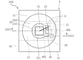
〔第2実施形態〕
図8〜図10に基づき、本発明の第2実施形態にかかるLEDパッケージA20について説明する。図8は、LEDパッケージA20の平面図であり、理解の便宜上、蓋5を省略している。図9は、図8のIX−IX線に沿う断面図である。図10は、図8のX−X線に沿う断面図である。なお、図9および図10においては、蓋5を省略せずに図示している。本実施形態においては、LEDパッケージA20は、平面視矩形状である。
[Second Embodiment]
An LED package A20 according to the second embodiment of the present invention will be described with reference to FIGS. FIG. 8 is a plan view of the LED package A20, and the
本実施形態にかかるLEDパッケージA20は、先述したLEDパッケージA10に対し、基板1の平面視寸法およびケース4の構成が異なる。図8に示すように、基板1の平面視寸法は、LEDパッケージA10の基板1の平面視寸法よりも小とされている。また、図8〜図10に示すように、本実施形態にかかる反射面43は、支持面42から起立している第1反射面431と、端面41および第1反射面431につながり、かつ支持面42に対して傾斜している第2反射面432とを含む。また、第1反射面431と第2反射面432とが交差する境界部433の平面視形状は、円形状である。よって、ケース4の厚さ方向に対する第1反射面431の断面形状は、境界部433の平面視形状と同一で、かつ一様である。したがって、本実施形態にかかる貫通領域46は、支持面42、第1反射面431および境界部433により形成された形状が円柱状の部分と、端面41、第2反射面432および境界部433により形成された形状が円錐台の部分とによって形成される。
The LED package A20 according to the present embodiment differs from the above-described LED package A10 in the size of the
本実施形態においては、搭載面211に沿った方向において、素子主面311の中央から第1反射面431までの距離は、LEDパッケージA10における素子主面311の中央から支持面42と反射面43との境界までの距離に等しい。また、本実施形態においては、基板1の厚さ方向において、素子主面311は境界部433と基板1の主面11との間に位置している。
In the present embodiment, in the direction along the mounting
本実施形態によっても、LEDパッケージA20の低背化や小型化を図りつつ、光の取り出し効率を高くすることが可能となる。また、本実施形態にかかる反射面43は、支持面42から起立している第1反射面431と、端面41および第1反射面431につながり、かつ支持面42に対して傾斜している第2反射面432とを含む。このような構成をとることによって、基板1およびケース4の平面視寸法を、LEDパッケージA10の当該寸法よりも小とすることができる。したがって、LEDパッケージA20は、LEDパッケージA10よりもさらに小型化とすることができる。
Also according to the present embodiment, it is possible to increase the light extraction efficiency while reducing the height and size of the LED package A20. The
〔第2実施形態の第1変形例〕
図11に基づき、本発明の第2実施形態の第1変形例にかかるLEDパッケージA21について説明する。図11は、LEDパッケージA21の断面図であり、その断面位置は図9と同一である。
[First Modification of Second Embodiment]
An LED package A21 according to a first modification of the second embodiment of the present invention will be described based on FIG. FIG. 11 is a sectional view of the LED package A21, and its sectional position is the same as that of FIG.
本変形例のLEDパッケージA21は、先述したLEDパッケージA20に対し、封止樹脂7を備える。封止樹脂7の材料および形状などは、先述したLEDパッケージA11と同様である。なお、LEDパッケージA21の基板1には、LEDパッケージA20と異なり、通気孔15が形成されていない。
The LED package A21 of this modified example is provided with the sealing resin 7 in addition to the LED package A20 described above. The material and shape of the sealing resin 7 are the same as those of the LED package A11 described above. Unlike the LED package A20, the
本変形例によっても、LEDパッケージA21の低背化や小型化を図りつつ、光の取り出し効率を高くすることが可能となる。また、LEDパッケージA21は、貫通領域46の一部を充填する封止樹脂7を備えることによって、LEDパッケージA11と同様の作用効果が得られ、LEDパッケージA20よりも光の取り出し効率をさらに高くすることが可能となる。
Also according to this modification, it is possible to increase the light extraction efficiency while reducing the height and size of the LED package A21. Further, the LED package A21 is provided with the sealing resin 7 that fills a part of the through
〔第2実施形態の第2変形例〕
図12に基づき、本発明の第2実施形態の第2変形例にかかるLEDパッケージA22について説明する。図12は、LEDパッケージA22の断面図であり、その断面位置は図9と同一である。
[Second Modification of Second Embodiment]
An LED package A22 according to a second modification of the second embodiment of the present invention will be described based on FIG. FIG. 12 is a sectional view of the LED package A22, and its sectional position is the same as that of FIG.
本変形例のLEDパッケージA22は、先述したLEDパッケージA20に対し、封止樹脂7を備える。封止樹脂7の材料および形状などは、先述したLEDパッケージA12と同様である。なお、LEDパッケージA22の基板1には、LEDパッケージA20と異なり、通気孔15が形成されていない。
The LED package A22 of this modified example is provided with the sealing resin 7 in addition to the LED package A20 described above. The material and shape of the sealing resin 7 are the same as those of the LED package A12 described above. Unlike the LED package A20, the
本変形例によっても、LEDパッケージA22の低背化や小型化を図りつつ、光の取り出し効率を高くすることが可能となる。また、LEDパッケージA22は、貫通領域46の全部を充填する封止樹脂7を備えることによって、LEDパッケージA12と同様の作用効果が得られ、先述したLEDパッケージA21よりも光の取り出し効率をさらに高くすることが可能となる。
Also according to this modification, it is possible to increase the light extraction efficiency while reducing the height and size of the LED package A22. Further, the LED package A22 is provided with the sealing resin 7 that fills the entire penetrating
〔第3実施形態〕
図13〜図16に基づき、本発明の第3実施形態にかかるLEDパッケージA30について説明する。図13は、LEDパッケージA30の平面図であり、理解の便宜上、蓋5を省略している。図14は、LEDパッケージA30の底面図である。図15は、図13のXV−XV線に沿う断面図である。図16は、図13のXVI−XVI線に沿う断面図である。なお、図15および図16においては、蓋5を省略せずに図示している。本実施形態においては、LEDパッケージA30は、平面視矩形状である。
[Third Embodiment]
An LED package A30 according to the third embodiment of the present invention will be described with reference to FIGS. FIG. 13 is a plan view of the LED package A30, and the
本実施形態にかかるLEDパッケージA30は、先述したLEDパッケージA10に対し、基板1、導電部21およびケース4の構成が異なる。本実施形態にかかる基板1は、図13、図15および図16に示すように、主面11、実装面12および複数の基板側面13に加えて、開口部14を有する。開口部14は、主面11から窪む部分であり、本実施形態においては、主面11から実装面12に至って貫通している。開口部14から導電部21の搭載面211が露出し、搭載面211にLED素子31が搭載される。したがって、本実施形態においては、LED素子31の一部が開口部14に収容されている。
The LED package A30 according to the present embodiment is different from the above-described LED package A10 in the configurations of the
本実施形態にかかる導電部21は、図14〜図16に示すように、めっき層212に加えて金属箔213を含む。金属箔213は、一部が基板1の実装面12から開口部14を塞ぎ、他の部分が実装面12に接する部分である。このため、開口部14は、金属箔213により実装面12から閉塞されている。金属箔213は、全体がめっき層212に覆われている。本実施形態においては、金属箔213はCuからなる。金属箔213は、実装面12に接着剤などで固定されている。この場合において、主面11に形成された導電部21は、図13の右側に示すボンディングワイヤ6が接続された部分のみとなり、当該部分と実装面12に形成された金属箔213とを互いに導通させるための連絡導電部22が基板1内に形成されている。図15に示す連絡導電部22の上端がめっき層212に接し、図15に示す連絡導電部22の下端が金属箔213に接している。
As shown in FIGS. 14 to 16, the
なお、本実施形態にかかるケース4の構成は、先述したLEDパッケージA20と同一である。
The configuration of the
本実施形態によっても、LEDパッケージA30の低背化や小型化を図りつつ、光の取り出し効率を高くすることが可能となる。また、本実施形態によれば、基板1には開口部14が形成され、一部が開口部14に収容されるようにLED素子31が搭載面211に搭載されている。このような構成をとることによって、素子主面311の中央からレンズ部53までの鉛直距離が、LEDパッケージA10およびLEDパッケージA20よりも長く確保される。すなわち、LED素子31の発光部からレンズ部53までの焦点距離が長く確保されるため、LEDパッケージA30は、LEDパッケージA10およびLEDパッケージA20よりも光の取り出し効率をさらに高くすることが可能となる。
Also according to the present embodiment, it is possible to increase the light extraction efficiency while reducing the height and size of the LED package A30. Further, according to this embodiment, the
LEDパッケージA30のケース4の構成は、LEDパッケージA20のケース4の構成と同一であるため、LEDパッケージA30の寸法について、LEDパッケージA20の寸法と同程度とすることができる。
Since the configuration of the
〔第3実施形態の第1変形例〕
図17に基づき、本発明の第3実施形態の第1変形例にかかるLEDパッケージA31について説明する。図17は、LEDパッケージA31の断面図であり、その断面位置は図15と同一である。
[First Modification of Third Embodiment]
An LED package A31 according to a first modification of the third embodiment of the present invention will be described based on FIG. FIG. 17 is a sectional view of the LED package A31, and its sectional position is the same as that of FIG.
本変形例のLEDパッケージA31は、先述したLEDパッケージA30に対し、封止樹脂7を備える。封止樹脂7の材料および形状は、先述したLEDパッケージA11と同様である。この場合において、開口部14の全部が封止樹脂7により充填されている。なお、LEDパッケージA31の基板1には、LEDパッケージA30と異なり、通気孔15が形成されていない。
The LED package A31 of this modified example is provided with the sealing resin 7 in addition to the LED package A30 described above. The material and shape of the sealing resin 7 are the same as those of the LED package A11 described above. In this case, the
本変形例によっても、LEDパッケージA31の低背化や小型化を図りつつ、光の取り出し効率を高くすることが可能となる。また、LEDパッケージA31は、貫通領域46の一部を充填する封止樹脂7を備えることによって、LEDパッケージA11と同様の作用効果が得られ、LEDパッケージA30よりも光の取り出し効率をさらに高くすることが可能となる。
Also according to this modification, it is possible to reduce the height and size of the LED package A31 and increase the light extraction efficiency. Further, the LED package A31 includes the sealing resin 7 that fills a part of the penetrating
〔第3実施形態の第2変形例〕
図18に基づき、本発明の第3実施形態の第2変形例にかかるLEDパッケージA32について説明する。図18は、LEDパッケージA32の断面図であり、その断面位置は図15と同一である。
[Second Modification of Third Embodiment]
An LED package A32 according to a second modification of the third embodiment of the present invention will be described based on FIG. FIG. 18 is a sectional view of the LED package A32, and its sectional position is the same as that of FIG.
本変形例のLEDパッケージA32は、先述したLEDパッケージA30に対し、封止樹脂7を備える。封止樹脂7の材料は、先述したLEDパッケージA12と同様である。この場合において、貫通領域46および開口部14の全部が封止樹脂7により充填されている。なお、LEDパッケージA32の基板1には、LEDパッケージA30と異なり、通気孔15が形成されていない。
The LED package A32 of this modified example is provided with the sealing resin 7 in addition to the LED package A30 described above. The material of the sealing resin 7 is the same as that of the LED package A12 described above. In this case, the penetrating
本変形例によっても、LEDパッケージA32の低背化や小型化を図りつつ、光の取り出し効率を高くすることが可能となる。また、LEDパッケージA32は、貫通領域46および開口部14の全部を充填する封止樹脂7を備える。これによりLEDパッケージA32には、LEDパッケージA12と同様の作用効果が得られ、先述したLEDパッケージA31よりも光の取り出し効率をさらに高くすることが可能となる。
Also according to this modification, it is possible to increase the light extraction efficiency while reducing the height and size of the LED package A32. Further, the
〔第4実施形態〕
図19〜図22に基づき、本発明の第4実施形態にかかるLEDパッケージA40について説明する。図19は、LEDパッケージA40の平面図であり、理解の便宜上、蓋5を省略している。図20は、LEDパッケージA40の底面図である。図21は、図19のXXI−XXI線(図19に示す一点鎖線)に沿う断面図である。図22は、図19のXXII−XXII線に沿う断面図である。なお、図21および図22においては、蓋5を省略せずに図示している。本実施形態においては、LEDパッケージA40は、平面視矩形状である。
[Fourth Embodiment]
An LED package A40 according to the fourth embodiment of the present invention will be described with reference to FIGS. FIG. 19 is a plan view of the LED package A40, and the
本実施形態にかかるLEDパッケージA40は、先述したLEDパッケージA10に対し、基板1の平面視寸法およびケース4の構成が異なるとともに、ツェナーダイオード33を備える。基板1の平面視寸法は、LEDパッケージA10および先述したLEDパッケージA20の基板1の平面視寸法よりも、さらに小とされている。
The LED package A40 according to the present embodiment is different from the above-described LED package A10 in the size of the
図21および図22に示すように、本実施形態にかかるケース4は、LEDパッケージA20のケース4を基としたものである。このため、ケース4の反射面43は、第1反射面431および第2反射面432を含む構成となっている。また、本実施形態にかかるケース4は、中間面481および内側面482を有する。中間面481は、支持面42から端面41に向かって窪み、かつ一端が反射面43(本実施形態においては第2反射面432)につながる平たん面である。中間面481は、基板1の主面11に対向している。内側面482は、支持面42から起立し、かつ中間面481および支持面42を相互につなぐ面である。図19に示すように、本実施形態にかかる内側面482は、第1反射面431に滑らかにつながっている。また、中間面481および内側面482には、ともに鏡面めっき層44により覆われている。
As shown in FIGS. 21 and 22, the
図19、図21および図22に示すように、本実施形態にかかるケース4は、中間面481、内側面482および支持面42によって形成された中空領域である凹部48を有する。凹部48は、貫通領域46に通じている。この場合において、LED素子31と導電部21とを接続するボンディングワイヤ6の一部が、凹部48に収容されている。また、本実施形態においては、導電部21の搭載面211に搭載され、かつ凹部48に収容されたツェナーダイオード33を備える。
As shown in FIGS. 19, 21 and 22, the
ツェナーダイオード33は、図19および図21に示すように、LED素子31が搭載されている導電部21の搭載面211に搭載されている。あわせて、ツェナーダイオード33と、LED素子31およびツェナーダイオード33が搭載されていない導電部21とを接続するボンディングワイヤ6を備える。ボンディングワイヤ6は、ツェナーダイオード33とともにその全部が凹部48に収容されている。本実施形態においては、図21および図22に示すツェナーダイオード33の上面にn側電極(カソード)が、図21および図22に示すツェナーダイオード33の下面にp側電極(アノード)が形成されている。当該n側電極は、ボンディングワイヤ6を介してツェナーダイオード33が搭載されていない導電部21に導通している。また、当該p側電極は、接合層32を介してツェナーダイオード33が搭載されている導電部21に導通している。このため、ツェナーダイオード33は、LED素子31と並列接続されている。接合層32は、LED素子31と同様に、ツェナーダイオード33を導電部21の搭載面211に固着するために適用される。
As shown in FIGS. 19 and 21, the
なお、図20に示すように、基板1の実装面12に形成された導電部21の形状は、図2に示すLEDパッケージA10における導電部21の形状に近似している。
Note that, as shown in FIG. 20, the shape of the
また、本実施形態にかかるケース4は、LEDパッケージA20のケース4を基にしたものであるが、LEDパッケージA10のケース4を基にしたものでもよい。また、先述したLEDパッケージA30で適用されているケース4を、本実施形態にかかるケース4に替えて適用してもよい。
The
本実施形態によっても、LEDパッケージA40の低背化や小型化を図りつつ、光の取り出し効率を高くすることが可能となる。また、本実施形態にかかるケース4は、中間面481および内側面482を有する。この場合において、LED素子31と導電部21とを接続するボンディングワイヤ6の一部が、中間面481、内側面482および支持面42によってケース4に形成された凹部48に収容されている。このような構成をとることによって、基板1およびケース4の平面視寸法を、LEDパッケージA20の当該寸法よりもさらに小とすることができる。したがって、LEDパッケージA40は、LEDパッケージA20よりもさらに小型化とすることができる。
Also according to the present embodiment, it is possible to increase the light extraction efficiency while reducing the height and size of the LED package A40. Further, the
また、本実施形態においては、導電部21の搭載面211に搭載され、かつ凹部48に収容されたツェナーダイオード33を備える。ツェナーダイオード33は、LED素子31と並列接続されている。LEDパッケージA40においてこのような回路を構成することによって、たとえばLEDパッケージA40に対して逆方向の静電気が放電した場合、当該静電気はツェナーダイオード33を流れ、LED素子31には流れない。また、LEDパッケージA40に対して順方向の静電気が放電した場合、LED素子31に印加される電圧は常に一定の値以下となる。したがって、LEDパッケージA40に対して順方向および逆方向の静電気が放電しても、当該静電気によりLED素子31が破壊されることを防ぐことができる。あわせて、LED素子31に順方向の過電圧が印加されることを防ぐことができる。また、ツェナーダイオード33は凹部48に収容されるため、凹部48の空間を有効に活用することができる。
Further, in the present embodiment, the
〔第4実施形態の第1変形例〕
図23に基づき、本発明の第4実施形態の第1変形例にかかるLEDパッケージA41について説明する。図23は、LEDパッケージA41の断面図であり、その断面位置は図21と同一である。
[First Modification of Fourth Embodiment]
An LED package A41 according to a first modification of the fourth embodiment of the present invention will be described with reference to FIG. 23 is a cross-sectional view of the LED package A41, and its cross-sectional position is the same as that of FIG.
本変形例のLEDパッケージA41は、先述したLEDパッケージA40に対し、封止樹脂7を備える。封止樹脂7の材料および形状などは、先述したLEDパッケージA11と同様である。この場合において、凹部48の一部が封止樹脂7により充填されている。なお、凹部48の全部が封止樹脂7により充填されていてもよい。なお、LEDパッケージA41の基板1には、LEDパッケージA40と異なり、通気孔15が形成されていない。
The LED package A41 of this modified example is provided with a sealing resin 7 in addition to the LED package A40 described above. The material and shape of the sealing resin 7 are the same as those of the LED package A11 described above. In this case, a part of the
本変形例によっても、LEDパッケージA41の低背化や小型化を図りつつ、光の取り出し効率を高くすることが可能となる。また、LEDパッケージA41は、貫通領域46の一部を充填する封止樹脂7を備えることによって、LEDパッケージA11と同様の作用効果が得られ、LEDパッケージA40よりも光の取り出し効率をさらに高くすることが可能となる。
Also according to this modification, it is possible to increase the light extraction efficiency while reducing the height and size of the LED package A41. In addition, the LED package A41 includes the sealing resin 7 that fills a part of the penetrating
〔第4実施形態の第2変形例〕
図24に基づき、本発明の第4実施形態の第2変形例にかかるLEDパッケージA42について説明する。図24は、LEDパッケージA42の断面図であり、その断面位置は図21と同一である。
[Second Modification of Fourth Embodiment]
An LED package A42 according to a second modification of the fourth embodiment of the present invention will be described based on FIG. 24 is a cross-sectional view of the LED package A42, and its cross-sectional position is the same as that of FIG.
本変形例のLEDパッケージA42は、先述したLEDパッケージA40に対し、封止樹脂7を備える。封止樹脂7の材料および形状などは、先述したLEDパッケージA12と同様である。この場合において、凹部48の全部が封止樹脂7により充填されている。なお、LEDパッケージA42の基板1には、LEDパッケージA40と異なり、通気孔15が形成されていない。
The LED package A42 of the present modification example is provided with the sealing resin 7 in addition to the LED package A40 described above. The material and shape of the sealing resin 7 are the same as those of the LED package A12 described above. In this case, the
本変形例によっても、LEDパッケージA42の低背化や小型化を図りつつ、光の取り出し効率を高くすることが可能となる。また、LEDパッケージA42は、貫通領域46の全部を充填する封止樹脂7を備えることによって、LEDパッケージA12と同様の作用効果が得られ、先述したLEDパッケージA41よりも光の取り出し効率をさらに高くすることが可能となる。
Also according to this modification, it is possible to increase the light extraction efficiency while reducing the height and size of the LED package A42. Further, the LED package A42 is provided with the sealing resin 7 that fills the entire penetrating
〔第5実施形態〕
図25および図26に基づき、本発明の第5実施形態にかかるLEDパッケージA50について説明する。図25は、LEDパッケージA50の平面図であり、理解の便宜上、蓋5を省略している。図26は、図25のXXVI−XXVI線(図25に示す一点鎖線)に沿う断面図である。なお、図26においては、蓋5を省略せずに図示している。本実施形態においては、LEDパッケージA50は、平面視矩形状である。
[Fifth Embodiment]
An LED package A50 according to the fifth embodiment of the present invention will be described with reference to FIGS. 25 and 26. FIG. 25 is a plan view of the LED package A50, and the
本実施形態にかかるLEDパッケージA50は、先述したLEDパッケージA40に対し、ケース4の構成が異なる。なお、基板1の平面視寸法は、LEDパッケージA40と同一とされている。
The LED package A50 according to the present embodiment differs from the above-described LED package A40 in the configuration of the
図25および図26に示すように、本実施形態にかかるケース4は、LEDパッケージA40を基としたものである。また、本実施形態にかかるケース4には、切欠部49が形成されている。切欠部49は、貫通領域46と凹部48との間に介在し、かつ中間面481および中間面481につながる反射面43(本実施形態では第2反射面432)との各々一部ずつが除去されることによって現れる空間である。LED素子31と導電部21とを接続するボンディングワイヤ6が、切欠部49を通過している。
As shown in FIGS. 25 and 26, the
本実施形態によっても、LEDパッケージA50の低背化や小型化を図りつつ、光の取り出し効率を高くすることが可能となる。また、本実施形態にかかるケース4には、切欠部49が形成され、LED素子31と導電部21とを接続するボンディングワイヤ6が、切欠部49を通過している。LEDパッケージA40のような凹部48が形成されたケース4を基板1に配置するとき、LED素子31と導電部21とを接続するボンディングワイヤ6の形状によっては、このボンディングワイヤ6が中間面481に接触して損傷する可能性がある。そこで、ケース4に切欠部49を形成することによって、LED素子31と導電部21とを接続するボンディングワイヤ6が、中間面481に接触して損傷することを防ぐことができる。
Also according to the present embodiment, it is possible to increase the light extraction efficiency while reducing the height and size of the LED package A50. Further, the
〔第5実施形態の第1変形例〕
図27に基づき、本発明の第5実施形態の第1変形例にかかるLEDパッケージA51について説明する。図27は、LEDパッケージA51の断面図であり、その断面位置は図26と同一である。
[First Modification of Fifth Embodiment]
An LED package A51 according to a first modification of the fifth embodiment of the present invention will be described with reference to FIG. FIG. 27 is a sectional view of the LED package A51, and its sectional position is the same as that of FIG.
本変形例のLEDパッケージA51は、先述したLEDパッケージA50に対し、封止樹脂7を備える。封止樹脂7の材料および形状などは、先述したLEDパッケージA11と同様である。この場合において、凹部48および切欠部49の各々一部ずつが封止樹脂7により充填されている。なお、凹部48の全部が封止樹脂7により充填されていてもよい。なお、LEDパッケージA51の基板1には、LEDパッケージA50と異なり、通気孔15が形成されていない。
The LED package A51 of this modified example is provided with a sealing resin 7 in addition to the LED package A50 described above. The material and shape of the sealing resin 7 are the same as those of the LED package A11 described above. In this case, the
本変形例によっても、LEDパッケージA51の低背化や小型化を図りつつ、光の取り出し効率を高くすることが可能となる。また、LEDパッケージA51は、貫通領域46の一部を充填する封止樹脂7を備えることによって、LEDパッケージA11と同様の作用効果が得られ、LEDパッケージA50よりも光の取り出し効率をさらに高くすることが可能となる。
Also according to this modification, it is possible to increase the light extraction efficiency while reducing the height and size of the LED package A51. Further, the LED package A51 is provided with the sealing resin 7 that fills a part of the penetrating
〔第5実施形態の第2変形例〕
図28に基づき、本発明の第5実施形態の第2変形例にかかるLEDパッケージA52について説明する。図28は、LEDパッケージA52の断面図であり、その断面位置は図26と同一である。
[Second Modification of Fifth Embodiment]
Based on FIG. 28, an LED package A52 according to a second modification of the fifth embodiment of the present invention will be described. 28 is a cross-sectional view of the LED package A52, and the cross-sectional position is the same as that of FIG.
本変形例のLEDパッケージA52は、先述したLEDパッケージA50に対し、封止樹脂7を備える。封止樹脂7の材料および形状などは、先述したLEDパッケージA12と同様である。この場合において、凹部48および切欠部49の全部が封止樹脂7により充填されている。なお、LEDパッケージA52の基板1には、LEDパッケージA50と異なり、通気孔15が形成されていない。
The LED package A52 of the present modification is provided with the sealing resin 7 in addition to the LED package A50 described above. The material and shape of the sealing resin 7 are the same as those of the LED package A12 described above. In this case, the
本変形例によっても、LEDパッケージA52の低背化や小型化を図りつつ、光の取り出し効率を高くすることが可能となる。また、LEDパッケージA52は、貫通領域46の全部を充填する封止樹脂7を備えることによって、LEDパッケージA12と同様の作用効果が得られ、先述したLEDパッケージA51よりも光の取り出し効率をさらに高くすることが可能となる。
Also according to this modification, it is possible to increase the light extraction efficiency while reducing the height and size of the LED package A52. Further, the LED package A52 is provided with the sealing resin 7 that fills the entire penetrating
〔第6実施形態〕
図29〜図31に基づき、本発明の第6実施形態にかかるLEDパッケージA60について説明する。図29は、LEDパッケージA60の平面図である。図30は、図29のXXX−XXX線に沿う断面図である。図31は、図30の部分拡大図である。本実施形態においては、LEDパッケージA60は、平面視矩形状である。
[Sixth Embodiment]
An LED package A60 according to the sixth embodiment of the present invention will be described with reference to FIGS. FIG. 29 is a plan view of the LED package A60. FIG. 30 is a sectional view taken along line XXX-XXX in FIG. FIG. 31 is a partially enlarged view of FIG. In the present embodiment, the LED package A60 has a rectangular shape in plan view.
本実施形態にかかるLEDパッケージA60は、先述したLEDパッケージA10に対し、蓋5の構成が異なる。
The LED package A60 according to the present embodiment is different from the above-described LED package A10 in the configuration of the
図29および図30に示すように、本実施形態にかかる蓋5には、プリズム部54が形成されている。プリズム部54は、各々が蓋5の頂面51に対して傾斜する第1傾斜面541および第2傾斜面542を有する。図31に示すように、第1傾斜面541および第2傾斜面542は、各々の一端が頂面51につながり、かつ各々の他端が相互につながっている。また、頂面51と第1傾斜面541とがなす鋭角αは、頂面51と第2傾斜面542とがなす鋭角βよりも小である。
As shown in FIGS. 29 and 30, a
図29に示すように、プリズム部54は、平面視において一方向に延出している。また、ケース4の貫通領域46の一部がプリズム部54に重なる。本実施形態にかかるプリズム部54は、互いに離間した状態で蓋5に複数形成されている。各々のプリズム部54は、いずれも蓋5の頂面51に囲まれている。このため、本実施形態にかかる頂面51の形状は、プリズム部54が占める領域がなすスリットを複数有する枠状である。
As shown in FIG. 29, the
本実施形態にかかるLEDパッケージA60は、LEDパッケージA10の蓋5の構成を変更したものである。本実施形態にかかる蓋5は、LEDパッケージA20、A30、A40およびA50のいずれにも適用することが可能である。
The LED package A60 according to the present embodiment is obtained by changing the configuration of the
本実施形態によっても、LEDパッケージA60の低背化や小型化を図りつつ、光の取り出し効率を高くすることが可能となる。また、本実施形態にかかる蓋5には、各々の一端が頂面51につながる第1傾斜面541および第2傾斜面542を有するプリズム部54が形成されている。この場合において、頂面51と第1傾斜面541とのなす鋭角αは、頂面51と第2傾斜面542とのなす鋭角βよりも小である。このような構成をとることによって、LED素子31から発せられ蓋5を透過する光が第1傾斜面541において、ある一定の方向に屈折する。したがって、LEDパッケージA60から出射される光を所定の方向に偏光させることができる。
Also according to the present embodiment, it is possible to increase the light extraction efficiency while reducing the height and size of the LED package A60. Further, the
〔第6実施形態の第1変形例〕
図32に基づき、本発明の第6実施形態の第1変形例にかかるLEDパッケージA61について説明する。図32は、LEDパッケージA61の断面図であり、その断面位置は図30と同一である。
[First Modification of Sixth Embodiment]
An LED package A61 according to a first modification of the sixth embodiment of the present invention will be described with reference to FIG. 32 is a cross-sectional view of the LED package A61, and its cross-sectional position is the same as that of FIG.
本変形例のLEDパッケージA61は、先述したLEDパッケージA60に対し、封止樹脂7を備える。封止樹脂7の材料および形状などは、先述したLEDパッケージA11と同様である。なお、LEDパッケージA61の基板1には、LEDパッケージA60と異なり、通気孔15が形成されていない。
The LED package A61 of this modified example is provided with the sealing resin 7 in addition to the LED package A60 described above. The material and shape of the sealing resin 7 are the same as those of the LED package A11 described above. Unlike the LED package A60, the
本変形例によっても、LEDパッケージA61の低背化や小型化を図りつつ、光の取り出し効率を高くすることが可能となる。また、LEDパッケージA61は、貫通領域46の一部を充填する封止樹脂7を備えることによって、LEDパッケージA11と同様の作用効果が得られ、LEDパッケージA60よりも光の取り出し効率をさらに高くすることが可能となる。
Also according to this modification, it is possible to increase the light extraction efficiency while reducing the height and size of the LED package A61. Further, the LED package A61 is provided with the sealing resin 7 that fills a part of the through
〔第6実施形態の第2変形例〕
図33に基づき、本発明の第6実施形態の第2変形例にかかるLEDパッケージA62について説明する。図33は、LEDパッケージA62の断面図であり、その断面位置は図30と同一である。
[Second Modification of Sixth Embodiment]
An LED package A62 according to a second modification of the sixth embodiment of the present invention will be described with reference to FIG. FIG. 33 is a sectional view of the LED package A62, and its sectional position is the same as that of FIG.
本変形例のLEDパッケージA62は、先述したLEDパッケージA60に対し、封止樹脂7を備える。封止樹脂7の材料および形状などは、先述したLEDパッケージA12と同様である。なお、LEDパッケージA62の基板1には、LEDパッケージA60と異なり、通気孔15が形成されていない。
The LED package A62 of the present modification example is provided with the sealing resin 7 in addition to the LED package A60 described above. The material and shape of the sealing resin 7 are the same as those of the LED package A12 described above. Unlike the LED package A60, the
本変形例によっても、LEDパッケージA62の低背化や小型化を図りつつ、光の取り出し効率を高くすることが可能となる。また、LEDパッケージA62は、貫通領域46の全部を充填する封止樹脂7を備えることによって、LEDパッケージA12と同様の作用効果が得られ、先述したLEDパッケージA61よりも光の取り出し効率をさらに高くすることが可能となる。
Also according to this modification, it is possible to increase the light extraction efficiency while reducing the height and size of the LED package A62. Further, the LED package A62 is provided with the encapsulating resin 7 that fills the entire penetrating
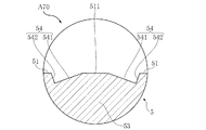
〔第7実施形態〕
図34〜図36に基づき、本発明の第7実施形態にかかるLEDパッケージA70について説明する。図34は、LEDパッケージA70の平面図である。図35は、図34のXXXV−XXXV線に沿う断面図である。図36は、図35の部分拡大図である。本実施形態においては、LEDパッケージA70は、平面視矩形状である。
[Seventh Embodiment]
An LED package A70 according to the seventh embodiment of the present invention will be described with reference to FIGS. 34 to 36. FIG. 34 is a plan view of the LED package A70. 35 is a sectional view taken along line XXXV-XXXV in FIG. 34. FIG. 36 is a partially enlarged view of FIG. In the present embodiment, the LED package A70 has a rectangular shape in plan view.
本実施形態にかかるLEDパッケージA70は、先述したLEDパッケージA60に対し、蓋5のプリズム部54の構成が異なる。
The LED package A70 according to the present embodiment differs from the above-described LED package A60 in the configuration of the
図34〜図36に示すように、蓋5の頂面51は、プリズム部54と同方向に延出する中央頂面511を含む。平面視においてLED素子31の一部が中央頂面511に重なる。中央頂面511が延出する方向と直角である方向における中央頂面511の両端に、プリズム部54の各々が位置し、かつ各々のプリズム部54の第1傾斜面541がつながっている。本実施形態にかかる蓋5には、中央頂面511の両側にプリズム部54が3つずつ形成され、各々のプリズム部の第1傾斜面541は、いずれも中央頂面511を挟んでLEDパッケージA70の外側を向いている。
As shown in FIGS. 34 to 36, the
本実施形態にかかるLEDパッケージA70は、LEDパッケージA60と同様に、LEDパッケージA10の蓋5の構成を変更したものである。本実施形態にかかる蓋5は、LEDパッケージA20、A30、A40およびA50のいずれにも適用することが可能である。
The LED package A70 according to the present embodiment is similar to the LED package A60 in that the configuration of the
本実施形態によっても、LEDパッケージA70の低背化や小型化を図りつつ、光の取り出し効率を高くすることが可能となる。また、本実施形態にかかる蓋5の頂面51は、プリズム部54と同方向に延出する中央頂面511を含み、中央頂面511の両端に、プリズム部54の各々が位置し、かつ各々のプリズム部54の第1傾斜面541がつながっている。このような構成をとることによって、LED素子31から発せられ蓋5を透過する光が、中央頂面511から透過する光の方向へ集約されるように屈折する。したがって、LEDパッケージA70から出射される光の相対強度を向上させることができる。この場合において、平面視においてLED素子31の一部が中央頂面511に重なる構成にすることによって、当該相対強度をより向上させることができる。
Also according to the present embodiment, it is possible to increase the light extraction efficiency while reducing the height and size of the LED package A70. Further, the
〔第7実施形態の第1変形例〕
図37に基づき、本発明の第7実施形態の第1変形例にかかるLEDパッケージA71について説明する。図37は、LEDパッケージA71の断面図であり、その断面位置は図35と同一である。
[First Modification of Seventh Embodiment]
An LED package A71 according to a first modification of the seventh embodiment of the present invention will be described with reference to FIG. FIG. 37 is a sectional view of the LED package A71, and its sectional position is the same as that of FIG.
本変形例のLEDパッケージA71は、先述したLEDパッケージA70に対し、封止樹脂7を備える。封止樹脂7の材料および形状などは、先述したLEDパッケージA11と同様である。なお、LEDパッケージA71の基板1には、LEDパッケージA70と異なり、通気孔15が形成されていない。
The LED package A71 of the present modification example is provided with the sealing resin 7 in addition to the LED package A70 described above. The material and shape of the sealing resin 7 are the same as those of the LED package A11 described above. In addition, unlike the LED package A70, the
本変形例によっても、LEDパッケージA71の低背化や小型化を図りつつ、光の取り出し効率を高くすることが可能となる。また、LEDパッケージA71は、貫通領域46の一部を充填する封止樹脂7を備えることによって、LEDパッケージA11と同様の作用効果が得られ、LEDパッケージA70よりも光の取り出し効率をさらに高くすることが可能となる。
Also according to this modification, it is possible to increase the light extraction efficiency while reducing the height and size of the LED package A71. In addition, the LED package A71 includes the sealing resin 7 that fills a part of the penetrating
〔第7実施形態の第2変形例〕
図38に基づき、本発明の第7実施形態の第2変形例にかかるLEDパッケージA72について説明する。図38は、LEDパッケージA72の断面図であり、その断面位置は図35と同一である。
[Second Modification of Seventh Embodiment]
An LED package A72 according to a second modification of the seventh embodiment of the present invention will be described with reference to FIG. 38 is a cross-sectional view of the LED package A72, and its cross-sectional position is the same as that of FIG.
本変形例のLEDパッケージA72は、先述したLEDパッケージA70に対し、封止樹脂7を備える。封止樹脂7の材料および形状などは、先述したLEDパッケージA12と同様である。なお、LEDパッケージA72の基板1には、LEDパッケージA70と異なり、通気孔15が形成されていない。
The LED package A72 of the present modification is provided with the sealing resin 7 in addition to the LED package A70 described above. The material and shape of the sealing resin 7 are the same as those of the LED package A12 described above. In addition, unlike the LED package A70, the
本変形例によっても、LEDパッケージA72の低背化や小型化を図りつつ、光の取り出し効率を高くすることが可能となる。また、LEDパッケージA72は、貫通領域46の全部を充填する封止樹脂7を備えることによって、LEDパッケージA12と同様の作用効果が得られ、先述したLEDパッケージA71よりも光の取り出し効率をさらに高くすることが可能となる。
Also according to this modification, it is possible to increase the light extraction efficiency while reducing the height and size of the LED package A72. Further, the LED package A72 is provided with the sealing resin 7 that fills the entire penetrating
〔第7実施形態の第3変形例〕
図39に基づき、本発明の第7実施形態の第3変形例にかかるLEDパッケージA73について説明する。図39は、LEDパッケージA73の平面図である。
[Third Modification of Seventh Embodiment]
An LED package A73 according to a third modification of the seventh embodiment of the present invention will be described with reference to FIG. FIG. 39 is a plan view of the LED package A73.
本変形例のLEDパッケージA73は、先述したLEDパッケージA70に対し、蓋5のプリズム部54の構成が異なる。各々のプリズム部54が延出する方向における両端の平面視形状は、貫通領域46の平面視形状に沿った円弧状である。
The LED package A73 of this modification is different from the above-described LED package A70 in the configuration of the
本変形例によっても、LEDパッケージA73の低背化や小型化を図りつつ、光の取り出し効率を高くすることが可能となる。 Also according to this modification, it is possible to increase the light extraction efficiency while reducing the height and size of the LED package A73.
本発明は、先述した実施形態やその変形例に限定されるものではない。本発明の各部の具体的な構成は、種々に設計変更自在である。 The present invention is not limited to the above-described embodiments and modifications thereof. The specific configuration of each part of the present invention can be modified in various ways.
A10,A11,A12:LEDパッケージ
A20,A21,A22:LEDパッケージ
A30,A31,A32:LEDパッケージ
A40,A41,A42:LEDパッケージ
A50,A51,A52:LEDパッケージ
A60,A61,A62:LEDパッケージ
A70,A71,A72,A73:LEDパッケージ
1:基板
11:主面
12:実装面
13:基板側面
14:開口部
21:導電部
211:搭載面
212:めっき層
213:金属箔
22:連絡導電部
31:LED素子
311:素子主面
312:素子裏面
32:接合層
4:ケース
41:端面
42:支持面
43:反射面
431:第1反射面
432:第2反射面
433:境界部
44:鏡面めっき層
45:ケース側面
46:貫通領域
47:接着層
48:凹部
481:中間面
482:内側面
49:切欠部
5:蓋
51:頂面
511:中央頂面
52:裏面
53:レンズ部
54:プリズム部
541:第1傾斜面
542:第2傾斜面
6:ボンディングワイヤ
7:封止樹脂
α,β:鋭角
A10, A11, A12: LED package A20, A21, A22: LED package A30, A31, A32: LED package A40, A41, A42: LED package A50, A51, A52: LED package A60, A61, A62: LED package A70, A71, A72, A73: LED package 1: substrate 11: main surface 12: mounting surface 13: substrate side surface 14: opening 21: conductive portion 211: mounting surface 212: plating layer 213: metal foil 22: contact conductive portion 31: LED element 311: Element main surface 312: Element back surface 32: Bonding layer 4: Case 41: End surface 42: Support surface 43: Reflection surface 431: First reflection surface 432: Second reflection surface 433: Boundary portion 44: Mirror surface plating layer 45: Side surface of case 46: Penetration region 47: Adhesive layer 48: Recessed portion 481: Intermediate surface 482: Inner side surface 49: Notch portion 5: Lid 51: Top surface 511: Central top surface 52: Back surface 53: Lens portion 54: Prism portion 541: first inclined surface 542: second inclined surface 6: bonding wire 7: sealing resin α, β: acute angle
Claims (28)
互いに反対側を向く主面および実装面を有する基板と、
前記主面と同一方向を向き、かつ前記LED素子が搭載される搭載面を有するとともに、前記主面および前記実装面の双方に形成された導電部と、
互いに反対側を向く端面および支持面、並びに前記端面および前記支持面につながるとともに前記LED素子を囲むように形成され、かつ前記支持面に対して傾斜した傾斜部を少なくとも含む反射面を有するとともに、前記支持面が前記主面に向くように配置されたケースと、
互いに反対側を向く頂面および裏面を有し、かつ前記裏面が前記端面を向くように前記ケースを覆う透光性がある蓋と、
前記LED素子と前記導電部とを接続するボンディングワイヤと、
前記搭載面に搭載されたツェナーダイオードと、を備え、
前記蓋には、前記裏面から前記LED素子に向かって突出した凸型のレンズ部が形成され、
前記ケースには、前記端面、前記支持面および前記反射面によって規定され、かつ前記端面および前記支持面の双方に対して平行に沿った断面積が、前記端面と前記反射面との境界において最も大である貫通領域が形成され、
前記レンズ部は、前記貫通領域に収容されるとともに、側面視において前記傾斜部に重なり、
前記ケースは、前記支持面から前記端面に向かって窪み、かつ一端が前記反射面につながる中間面と、前記中間面および前記支持面につながる内側面と、をさらに有し、
前記ケースには、前記中間面、前記内側面および前記支持面によって規定された凹部が形成され、
前記ボンディングワイヤの一部と、前記ツェナーダイオードの少なくとも一部と、が前記凹部に収容されていることを特徴とする、LEDパッケージ。 LED element,
A substrate having a main surface and a mounting surface facing opposite sides,
Can toward the main surface in the same direction, and as to have a mounting surface on which the LED element is mounted, and the main surface and the formed on both the mounting surface conductive portion,
End surface and the support surface facing away from each other, and are formed so as to surround the LED element with lead to the end surface and the supporting surface, and which has the support surface including at least reflecting surface inclined portion inclined with respect to, A case arranged so that the support surface faces the main surface,
A translucent lid having a top surface and a back surface facing opposite sides, and covering the case so that the back surface faces the end surface;
A bonding wire connecting the LED element and the conductive portion,
A Zener diode mounted on the mounting surface,
A convex lens portion protruding from the back surface toward the LED element is formed on the lid ,
In the case, a cross-sectional area defined by the end surface, the support surface and the reflection surface, and parallel to both the end surface and the support surface is the most at the boundary between the end surface and the reflection surface. A penetration area that is large is formed,
The lens portion is accommodated in the penetrating region and overlaps the inclined portion in a side view,
The case further has an intermediate surface that is recessed from the support surface toward the end surface and has one end connected to the reflection surface, and an inner surface connected to the intermediate surface and the support surface,
In the case, a recess defined by the intermediate surface, the inner surface and the support surface is formed,
An LED package , wherein a part of the bonding wire and at least a part of the Zener diode are housed in the recess .
前記ボンディングワイヤが、前記切欠部を通過している、請求項1に記載のLEDパッケージ。 In the case, a notch portion that is interposed between the penetrating region and the recessed portion and is formed by removing a part of each of the intermediate surface and the reflecting surface connected to the intermediate surface is formed,
The LED package according to claim 1, wherein the bonding wire passes through the cutout portion .
前記通気孔は、前記貫通領域に通じている、請求項1ないし4のいずれかに記載のLEDパッケージ。 The substrate is formed with a vent hole that penetrates from the main surface to the mounting surface and through which external air flows,
The LED package according to claim 1 , wherein the vent hole communicates with the penetrating region .
前記連絡導電部は、前記主面および前記実装面から露出している、請求項15または16に記載のLEDパッケージ。 Further comprising a connecting conductive portion formed inside the substrate and conducting to the conductive portion,
The LED package according to claim 15 or 16 , wherein the connecting conductive portion is exposed from the main surface and the mounting surface .
前記第1反射面と前記第2反射面とが交差する境界部の平面視形状は、円形状である、請求項19に記載のLEDパッケージ。 The reflecting surface includes a first reflecting surface which is erected from the support surface, leading to the end surface and the first reflecting surface and a second reflecting surface corresponding to the inclined portion,
The LED package according to claim 19 , wherein a plan view shape of a boundary portion where the first reflecting surface and the second reflecting surface intersect is circular.
前記基板の厚さ方向において、前記素子主面は、前記境界部と前記主面との間に位置している、請求項20に記載のLEDパッケージ。 The LED element has an element main surface on which a light emitting portion is formed,
In the thickness direction of the substrate, the element main surface is located between the main surface and the boundary portion, LED package according to claim 20.
前記導電部は、前記実装面に接し、かつ前記実装面から前記開口部を塞ぐ金属箔を含む、請求項22に記載のLEDパッケージ。 The opening penetrates from the main surface to the mounting surface,
The LED package according to claim 22, wherein the conductive portion includes a metal foil that is in contact with the mounting surface and closes the opening from the mounting surface .
前記複数のプリズム部の各々において、前記第1傾斜面および前記第2傾斜面は、前記頂面につながるとともに、互いにつながり、
前記頂面と前記第1傾斜面とがなす鋭角は、前記頂面と前記第2傾斜面とがなす鋭角よりも小である、請求項1ないし26のいずれかに記載のLEDパッケージ。 The lid has a first inclined surface and a second inclined surface that are inclined with respect to the top surface, and a plurality of prism portions that extend in one direction in a plan view and overlap a part of the penetrating region are formed. Is
In each of the plurality of prism portions, the first inclined surface and the second inclined surface are connected to the top surface and are connected to each other,
27. The LED package according to claim 1 , wherein an acute angle formed by the top surface and the first inclined surface is smaller than an acute angle formed by the top surface and the second inclined surface .
前記中央頂面は、前記複数のプリズム部のうち隣り合う2つの当該プリズム部の間に位置し、
前記2つの当該プリズム部の前記第1傾斜面は、前記中央頂面につながり、
平面視において前記LED素子の一部が前記中央頂面に重なっている、請求項27に記載のLEDパッケージ。 The top surface includes a central top surface extending in the same direction as the prism portion,
The central top surface is located between two adjacent prism portions of the plurality of prism portions,
The first inclined surfaces of the two relevant prism portions are connected to the central top surface,
The LED package according to claim 27, wherein a part of the LED element overlaps with the central top surface in a plan view .
Priority Applications (1)
| Application Number | Priority Date | Filing Date | Title |
|---|---|---|---|
| US15/264,215 US10355183B2 (en) | 2015-09-18 | 2016-09-13 | LED package |
Applications Claiming Priority (2)
| Application Number | Priority Date | Filing Date | Title |
|---|---|---|---|
| JP2015185522 | 2015-09-18 | ||
| JP2015185522 | 2015-09-18 |
Publications (3)
| Publication Number | Publication Date |
|---|---|
| JP2017059818A JP2017059818A (en) | 2017-03-23 |
| JP2017059818A5 JP2017059818A5 (en) | 2019-06-20 |
| JP6738224B2 true JP6738224B2 (en) | 2020-08-12 |
Family
ID=58391824
Family Applications (1)
| Application Number | Title | Priority Date | Filing Date |
|---|---|---|---|
| JP2016142006A Active JP6738224B2 (en) | 2015-09-18 | 2016-07-20 | LED package |
Country Status (1)
| Country | Link |
|---|---|
| JP (1) | JP6738224B2 (en) |
Families Citing this family (5)
| Publication number | Priority date | Publication date | Assignee | Title |
|---|---|---|---|---|
| JP6944660B2 (en) * | 2018-02-27 | 2021-10-06 | 東芝ライテック株式会社 | Vehicle lighting equipment and vehicle lighting equipment |
| US10461231B2 (en) * | 2018-02-27 | 2019-10-29 | Lumens Co., Ltd. | Method for fabricating LED package |
| KR102094402B1 (en) | 2018-08-24 | 2020-03-27 | 주식회사 케이티앤지 | Light emitting element and Aerosol generating device including the same |
| JP6675032B1 (en) * | 2019-07-08 | 2020-04-01 | 御田 護 | Semiconductor light emitting device |
| KR102415673B1 (en) * | 2020-09-24 | 2022-07-05 | 주식회사 엠엘케이 | Tiny led flexible module circuit board |
Family Cites Families (7)
| Publication number | Priority date | Publication date | Assignee | Title |
|---|---|---|---|---|
| JP2001338505A (en) * | 2000-05-26 | 2001-12-07 | Matsushita Electric Works Ltd | Lighting device |
| JP4789673B2 (en) * | 2005-10-27 | 2011-10-12 | 京セラ株式会社 | Light emitting element storage package, and light source and light emitting device using the same |
| JP5233170B2 (en) * | 2007-05-31 | 2013-07-10 | 日亜化学工業株式会社 | LIGHT EMITTING DEVICE, RESIN MOLDED BODY FORMING LIGHT EMITTING DEVICE, AND METHOD FOR PRODUCING THEM |
| JP2009277705A (en) * | 2008-05-12 | 2009-11-26 | Koa Corp | Package light-emitting component and method of manufacturing the same |
| JP2012015438A (en) * | 2010-07-05 | 2012-01-19 | Citizen Holdings Co Ltd | Semiconductor light emitting device |
| KR20130098048A (en) * | 2012-02-27 | 2013-09-04 | 엘지이노텍 주식회사 | Light emitting device package |
| CN104752369B (en) * | 2013-12-27 | 2018-02-16 | 展晶科技(深圳)有限公司 | Photoelectric cell module |
-
2016
- 2016-07-20 JP JP2016142006A patent/JP6738224B2/en active Active
Also Published As
| Publication number | Publication date |
|---|---|
| JP2017059818A (en) | 2017-03-23 |
Similar Documents
| Publication | Publication Date | Title |
|---|---|---|
| US10355183B2 (en) | LED package | |
| JP6738224B2 (en) | LED package | |
| JP5768435B2 (en) | Light emitting device | |
| US7994518B2 (en) | Light-emitting diode | |
| US20110163338A1 (en) | Light emitting device and method of manufacturing the same | |
| TW201727945A (en) | Light emitting device | |
| JP2017130640A (en) | Light-emitting device | |
| KR20090044306A (en) | Light emitting diode package | |
| JP5939977B2 (en) | LED module | |
| JP4913099B2 (en) | Light emitting device | |
| KR101762597B1 (en) | Substrate for semiconductor light emitting device | |
| JP2011192682A (en) | Optical semiconductor package and optical semiconductor device | |
| KR20140004351A (en) | Light emitting diode package | |
| JP2010283063A (en) | Light emitting device and light emitting module | |
| KR102634692B1 (en) | Semiconductor light emitting device package | |
| KR20120030475A (en) | Light emitting diode package | |
| JP2022046071A (en) | Light emitting device | |
| JP6399057B2 (en) | Light emitting device | |
| KR101863549B1 (en) | Semiconductor light emitting device | |
| JP5296266B2 (en) | Light emitting device | |
| JP2013187269A (en) | Optical semiconductor device and manufacturing method of the same | |
| KR102008286B1 (en) | Light emitting device and lighting unit using the same | |
| KR101806790B1 (en) | Semiconductor light emitting device | |
| KR101125456B1 (en) | Light emitting device and light unit using the same | |
| KR101946244B1 (en) | Semiconductor light emitting device |
Legal Events
| Date | Code | Title | Description |
|---|---|---|---|
| A521 | Request for written amendment filed |
Free format text: JAPANESE INTERMEDIATE CODE: A523 Effective date: 20190516 |
|
| A621 | Written request for application examination |
Free format text: JAPANESE INTERMEDIATE CODE: A621 Effective date: 20190621 |
|
| A977 | Report on retrieval |
Free format text: JAPANESE INTERMEDIATE CODE: A971007 Effective date: 20200527 |
|
| TRDD | Decision of grant or rejection written | ||
| A01 | Written decision to grant a patent or to grant a registration (utility model) |
Free format text: JAPANESE INTERMEDIATE CODE: A01 Effective date: 20200623 |
|
| A61 | First payment of annual fees (during grant procedure) |
Free format text: JAPANESE INTERMEDIATE CODE: A61 Effective date: 20200717 |
|
| R150 | Certificate of patent or registration of utility model |
Ref document number: 6738224 Country of ref document: JP Free format text: JAPANESE INTERMEDIATE CODE: R150 |
|
| R250 | Receipt of annual fees |
Free format text: JAPANESE INTERMEDIATE CODE: R250 |