JP6736552B6 - タイミング回路構成を備える感知素子を有する容量性指紋センサ - Google Patents
タイミング回路構成を備える感知素子を有する容量性指紋センサ Download PDFInfo
- Publication number
- JP6736552B6 JP6736552B6 JP2017530001A JP2017530001A JP6736552B6 JP 6736552 B6 JP6736552 B6 JP 6736552B6 JP 2017530001 A JP2017530001 A JP 2017530001A JP 2017530001 A JP2017530001 A JP 2017530001A JP 6736552 B6 JP6736552 B6 JP 6736552B6
- Authority
- JP
- Japan
- Prior art keywords
- signal
- circuitry
- sensing
- charge
- potential
- Prior art date
- Legal status (The legal status is an assumption and is not a legal conclusion. Google has not performed a legal analysis and makes no representation as to the accuracy of the status listed.)
- Expired - Fee Related
Links
Images


Classifications
-
- G—PHYSICS
- G06—COMPUTING OR CALCULATING; COUNTING
- G06V—IMAGE OR VIDEO RECOGNITION OR UNDERSTANDING
- G06V40/00—Recognition of biometric, human-related or animal-related patterns in image or video data
- G06V40/10—Human or animal bodies, e.g. vehicle occupants or pedestrians; Body parts, e.g. hands
- G06V40/12—Fingerprints or palmprints
- G06V40/13—Sensors therefor
- G06V40/1329—Protecting the fingerprint sensor against damage caused by the finger
-
- G—PHYSICS
- G06—COMPUTING OR CALCULATING; COUNTING
- G06V—IMAGE OR VIDEO RECOGNITION OR UNDERSTANDING
- G06V40/00—Recognition of biometric, human-related or animal-related patterns in image or video data
- G06V40/10—Human or animal bodies, e.g. vehicle occupants or pedestrians; Body parts, e.g. hands
- G06V40/12—Fingerprints or palmprints
- G06V40/13—Sensors therefor
- G06V40/1306—Sensors therefor non-optical, e.g. ultrasonic or capacitive sensing
-
- G—PHYSICS
- G01—MEASURING; TESTING
- G01R—MEASURING ELECTRIC VARIABLES; MEASURING MAGNETIC VARIABLES
- G01R27/00—Arrangements for measuring resistance, reactance, impedance, or electric characteristics derived therefrom
- G01R27/02—Measuring real or complex resistance, reactance, impedance, or other two-pole characteristics derived therefrom, e.g. time constant
- G01R27/26—Measuring inductance or capacitance; Measuring quality factor, e.g. by using the resonance method; Measuring loss factor; Measuring dielectric constants ; Measuring impedance or related variables
- G01R27/2605—Measuring capacitance
-
- G—PHYSICS
- G06—COMPUTING OR CALCULATING; COUNTING
- G06F—ELECTRIC DIGITAL DATA PROCESSING
- G06F3/00—Input arrangements for transferring data to be processed into a form capable of being handled by the computer; Output arrangements for transferring data from processing unit to output unit, e.g. interface arrangements
- G06F3/01—Input arrangements or combined input and output arrangements for interaction between user and computer
- G06F3/03—Arrangements for converting the position or the displacement of a member into a coded form
- G06F3/033—Pointing devices displaced or positioned by the user, e.g. mice, trackballs, pens or joysticks; Accessories therefor
- G06F3/0354—Pointing devices displaced or positioned by the user, e.g. mice, trackballs, pens or joysticks; Accessories therefor with detection of two-dimensional [2D] relative movements between the device, or an operating part thereof, and a plane or surface, e.g. 2D mice, trackballs, pens or pucks
- G06F3/03547—Touch pads, in which fingers can move on a surface
-
- G—PHYSICS
- G07—CHECKING-DEVICES
- G07C—TIME OR ATTENDANCE REGISTERS; REGISTERING OR INDICATING THE WORKING OF MACHINES; GENERATING RANDOM NUMBERS; VOTING OR LOTTERY APPARATUS; ARRANGEMENTS, SYSTEMS OR APPARATUS FOR CHECKING NOT PROVIDED FOR ELSEWHERE
- G07C9/00—Individual registration on entry or exit
-
- A—HUMAN NECESSITIES
- A61—MEDICAL OR VETERINARY SCIENCE; HYGIENE
- A61B—DIAGNOSIS; SURGERY; IDENTIFICATION
- A61B2562/00—Details of sensors; Constructional details of sensor housings or probes; Accessories for sensors
- A61B2562/02—Details of sensors specially adapted for in-vivo measurements
- A61B2562/0209—Special features of electrodes classified in A61B5/24, A61B5/25, A61B5/283, A61B5/291, A61B5/296, A61B5/053
- A61B2562/0214—Capacitive electrodes
Landscapes
- Engineering & Computer Science (AREA)
- Physics & Mathematics (AREA)
- General Physics & Mathematics (AREA)
- Theoretical Computer Science (AREA)
- Human Computer Interaction (AREA)
- General Engineering & Computer Science (AREA)
- Multimedia (AREA)
- Image Input (AREA)
- Measurement Of Length, Angles, Or The Like Using Electric Or Magnetic Means (AREA)
- Measurement Of The Respiration, Hearing Ability, Form, And Blood Characteristics Of Living Organisms (AREA)
- Chemical & Material Sciences (AREA)
- Chemical Kinetics & Catalysis (AREA)
- Electrochemistry (AREA)
- Health & Medical Sciences (AREA)
- Life Sciences & Earth Sciences (AREA)
- Analytical Chemistry (AREA)
- Biochemistry (AREA)
- General Health & Medical Sciences (AREA)
- Immunology (AREA)
- Pathology (AREA)
Description
Claims (19)
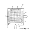
- 指(31)の指紋パターンを感知する容量性指紋感知装置であって、
前記容量性指紋感知装置は複数の感知素子(8)を備え、各感知素子は、
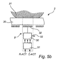
前記指(31)による接触対象である保護誘電最上層(30)の一部と、
前記最上層(30)の前記一部の下に配置される導電性感知構造(32)と、
電荷測定回路構成(50)であって、前記感知構造に接続されて、少なくとも第一の測定状態と第二の測定状態との間を連続的に遷移して測定シーケンスを実行し、前記指と前記感知構造との間の電位差の変化に起因して前記感知構造が帯びる電荷に生じる変化を示す出力信号を前記電荷測定回路構成から発信する、電荷測定回路構成と、
前記電荷測定回路構成に接続されて前記測定状態の少なくとも一つのタイミングを制御するタイミング回路構成(51)と、
を備え、
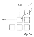
前記タイミング回路構成は、第一の事象と前記第一の事象に関する時間遅延とによって規定される遷移時間で前記第一の測定状態から前記第二の測定状態に遷移するように前記電荷測定回路構成を制御するように構成され、
前記タイミング回路構成は、前記第一の事象を規定する第一の信号を受信する入力と、前記第一の事象に対して遅延する第二の事象を規定する第二の信号を供給する出力と、を有する第一の遅延素子を備え、
前記タイミング回路構成は、前記第一の遅延素子の出力と第二の遅延素子の入力との間に連結される少なくとも一つの論理ゲートを更に備える、
容量性指紋感知装置。 - 前記第二の事象は、前記第一の測定状態から第二の測定状態への遷移を含む、請求項1に記載の容量性指紋感知装置。
- 前記第一の遅延素子の出力は、前記電荷測定回路構成に連結されて、前記第二の信号によって前記電荷測定回路構成の動作を制御できるようにする、請求項1又は請求項2に記載の容量性指紋感知装置。
- 前記タイミング回路構成は、前記第一の遅延素子の出力に連結される入力と、前記第二の事象に対して遅延する第三の事象を規定する第三の信号を供給する出力と、を有する第二の遅延素子を更に備える、請求項1から請求項3までのいずれか一項に記載の容量性指紋感知装置。
- 前記第二の遅延素子の出力は、前記電荷測定回路構成に連結されて、前記第三の信号によって前記電荷測定回路構成の動作を制御できるようにする、請求項4に記載の容量性指紋感知装置。
- 前記タイミング回路構成は、それぞれが入力及び出力を有する複数の遅延素子を備え、
前記遅延素子は、連続する遅延素子の配列の形状に配置され、連続する遅延素子の前記配列では前記遅延素子のぞれぞれの出力が次の素子の入力に連結されるようになる、
請求項1から請求項5までのいずれか一項に記載の容量性指紋感知装置。 - 前記配列は閉ループ配列である、請求項6に記載の容量性指紋感知装置。
- 前記第一の事象は、前記感知素子の外側で生成される起動信号によってもたらされる、請求項1から請求項7までのいずれか一項に記載の容量性指紋感知装置。
- 前記測定シーケンスは、前記電荷測定回路構成の出力での電位が前記感知構造の電位を基準とするリセット状態を少なくとも含む、請求項1から請求項8までのいずれか一項に記載の容量性指紋感知装置。
- 前記電荷測定回路構成は、
電荷増幅器であって、
前記感知構造に接続される負の入力と、
正の入力と、
出力と、
前記負の入力と前記出力との間に接続される帰還コンデンサと、
前記正及び負の入力と前記出力との間の少なくとも一つの増幅器段と、
を備える電荷増幅器を備え、
前記電荷増幅器は、前記負の入力での電位が前記正の入力での電位を実質的に追従するように構成される、
請求項1から請求項9までのいずれか一項に記載の容量性指紋感知装置。 - 前記容量性指紋感知装置は、
励起信号供給回路構成であって、前記正の入力に接続されて、前記正の入力での電位を第一の電位から第二の電位に変化させ、これにより前記感知構造の電位を変化させ、これにより前記指と前記感知構造との間の電位差の前記変化をもたらすように構成される励起信号供給回路構成、
を更に備える、請求項10に記載の容量性指紋感知装置。 - 前記タイミング回路構成は、前記励起信号供給回路構成に接続されて、
第一の励起制御信号を前記励起信号供給回路構成に供給して、第一の励起遷移時間での第一の電位から第二の電位への電位の前記変化を引き起こし、
第二の励起制御信号を前記励起信号供給回路構成に供給して、第二の励起遷移時間での第二の電位から第一の電位に戻る電位の変化を引き起こす、
請求項11に記載の容量性指紋感知装置。 - 指の指紋パターンを感知する容量性指紋感知装置であって、
前記容量性指紋感知装置は複数の感知素子を備え、各感知素子は、
前記指による接触対象である保護誘電最上層の一部と、
前記最上層の前記一部の下に配置される導電性感知構造と、
電荷測定回路構成であって、前記感知構造に接続されて、少なくとも第一の測定状態と第二の測定状態との間を連続的に遷移して測定シーケンスを実行し、前記指と前記感知構造との間の電位差の変化に起因して前記感知構造が帯びる電荷に生じる変化を示す出力信号を前記電荷測定回路構成から発信する、電荷測定回路構成と、
前記電荷測定回路構成に接続されて前記測定状態の少なくとも一つのタイミングを制御するタイミング回路構成と、
を備え、
前記指紋感知装置は、前記指の電位に対して第一の電位から第二の電位に変わり第一の電位に戻る循環変化を含み時間的に変化する励起電位を示す励起信号を供給する励起信号供給回路構成を更に備え、
前記感知素子のそれぞれは、復調回路構成であって、前記電荷測定回路構成に接続されて、前記電荷測定回路構成からの前記出力信号及びタイミングに関連する復調信号を前記励起信号に結合し、前記感知構造が帯びる電荷の前記変化を示すDC信号成分を含む結合信号を供給する復調回路構成を更に備え、
前記指紋感知装置は、読み出し回路構成であって、前記感知素子のそれぞれに接続されて、前記感知素子のそれぞれからの前記DC信号成分に基づく前記指紋パターンの表示を供給する読み出し回路構成を更に備える、
容量性指紋感知装置。 - 前記復調回路構成は、前記出力信号を前記復調信号とともに逓倍する信号逓倍回路構成を備える、請求項13に記載の容量性指紋感知装置。
- 前記復調回路構成は、高周波化した周波数成分を除去しながら前記DC信号成分が通過できるようにするローパスフィルタを更に備える、請求項13又は請求項14に記載の容量性指紋感知装置。
- 前記電荷測定回路構成は、
サンプリング回路構成であって、
前記指と前記感知構造との間の電位差の前記変化の前の第一のサンプリング時間に、前記感知構造が帯びる電荷を示す信号をサンプリングし、
前記指と前記感知構造との間の電位差の前記変化の後の第二のサンプリング時間に、前記感知構造が帯びる電荷を示す前記信号をサンプリングする、
サンプリング回路構成、
を備える、請求項1から請求項15までのいずれか一項に記載の容量性指紋感知装置。 - 前記タイミング回路構成は、前記サンプリング回路構成に接続されて、
第一のサンプリング制御信号を、前記第一のサンプリング時間に第一の信号のサンプリングを実施する前記サンプリング回路構成に供給し、
第二のサンプリング制御信号を、前記第二のサンプリング時間に第二の信号のサンプリングを実施する前記サンプリング回路構成に供給する、
請求項16に記載の容量性指紋感知装置。 - 前記感知素子のそれぞれに接続され、前記感知素子のそれぞれからの前記出力信号に基づく前記指紋パターンの表示を供給するように構成される読み出し回路構成、を更に備える、請求項1から請求項17までのいずれか一項に記載の容量性指紋感知装置。
- 電子装置であって、
請求項18に記載の指紋感知装置と、
処理回路構成であって、
指紋感知装置からの前記指紋パターンの前記表示を取得し、
前記表示に基づいてユーザを認証し、
前記表示に基づいて前記ユーザが認証された場合にのみ少なくとも一つのユーザ要求処理を実施する、
ように構成される処理回路構成と、
を備える電子装置。
Applications Claiming Priority (3)
| Application Number | Priority Date | Filing Date | Title |
|---|---|---|---|
| SE1451633 | 2014-12-22 | ||
| SE1451633-0 | 2014-12-22 | ||
| PCT/SE2015/051345 WO2016105261A1 (en) | 2014-12-22 | 2015-12-15 | Capacitive fingerprint sensor with sensing elements comprising timing circuitry |
Publications (3)
| Publication Number | Publication Date |
|---|---|
| JP2018500555A JP2018500555A (ja) | 2018-01-11 |
| JP6736552B2 JP6736552B2 (ja) | 2020-08-05 |
| JP6736552B6 true JP6736552B6 (ja) | 2020-09-02 |
Family
ID=56129784
Family Applications (1)
| Application Number | Title | Priority Date | Filing Date |
|---|---|---|---|
| JP2017530001A Expired - Fee Related JP6736552B6 (ja) | 2014-12-22 | 2015-12-15 | タイミング回路構成を備える感知素子を有する容量性指紋センサ |
Country Status (8)
| Country | Link |
|---|---|
| US (1) | US9449212B2 (ja) |
| EP (1) | EP3238134B1 (ja) |
| JP (1) | JP6736552B6 (ja) |
| KR (1) | KR101852043B1 (ja) |
| CN (1) | CN106062775B (ja) |
| DE (1) | DE112015005732T5 (ja) |
| TW (1) | TWI630555B (ja) |
| WO (1) | WO2016105261A1 (ja) |
Families Citing this family (22)
| Publication number | Priority date | Publication date | Assignee | Title |
|---|---|---|---|---|
| US8485442B2 (en) | 2009-07-02 | 2013-07-16 | Biometric Payment Solutions | Electronic transaction verification system with biometric authentication |
| US9600705B2 (en) * | 2015-02-11 | 2017-03-21 | Fingerprint Cards Ab | Capacitive fingerprint sensing device with current readout from sensing elements |
| SE1650548A1 (en) * | 2016-04-22 | 2017-10-23 | Fingerprint Cards Ab | Fingerprint sensing system with sensing reference potential providing circuitry |
| SE539638C2 (en) * | 2016-04-22 | 2017-10-24 | Fingerprint Cards Ab | Fingerprint sensing system with adaptive power control |
| US9864895B1 (en) * | 2016-07-07 | 2018-01-09 | Fingerprint Cards Ab | Fingerprint sensing system with finger detect |
| CN107918749A (zh) * | 2016-10-08 | 2018-04-17 | 深圳指瑞威科技有限公司 | 基于bcd工艺的高穿透能力的指纹传感器 |
| TWI736688B (zh) * | 2016-11-17 | 2021-08-21 | 瑞典商指紋卡公司 | 使用具有不同主要延伸方向的測量組態之指紋感測 |
| CN106796658A (zh) * | 2016-11-21 | 2017-05-31 | 深圳市汇顶科技股份有限公司 | 指纹传感器及电子终端 |
| US10395164B2 (en) * | 2016-12-15 | 2019-08-27 | Fingerprint Cards Ab | Fingerprint sensing module and method for manufacturing the fingerprint sensing module |
| US11610429B2 (en) | 2016-12-15 | 2023-03-21 | Fingerprint Cards Anacatum Ip Ab | Fingerprint sensing module and method for manufacturing the fingerprint sensing module |
| US10002280B1 (en) * | 2016-12-21 | 2018-06-19 | Fingerprint Cards Ab | System and method for controlling a signal in a fingerprint sensing device |
| EP3358496B1 (en) | 2017-02-02 | 2021-04-07 | Nxp B.V. | Fingerprint processing system and method |
| CN107122703B (zh) * | 2017-03-15 | 2019-12-17 | 深圳信炜科技有限公司 | 生物信息传感装置、电子设备和共模干扰检测方法 |
| CN108985150B (zh) | 2017-05-31 | 2022-05-27 | 联咏科技股份有限公司 | 电容式图像传感器 |
| EP3721659B1 (en) * | 2017-12-06 | 2022-06-15 | Fingerprint Cards Anacatum IP AB | Method for transitioning a device controller comprised in an electronic device, and an electronic device |
| TWI640778B (zh) | 2018-03-02 | 2018-11-11 | National Applied Research Laboratories | 訊號誤差校正方法 |
| US11015914B2 (en) * | 2019-01-21 | 2021-05-25 | Novatek Microelectronics Corp. | Capacitive image sensing device and capacitive image sensing method |
| CN113743156B (zh) * | 2020-05-28 | 2024-12-31 | 北京小米移动软件有限公司 | 指纹检测模组、电子设备、检测方法、装置及存储介质 |
| JP7491283B2 (ja) * | 2021-09-17 | 2024-05-28 | 株式会社豊田中央研究所 | センサ |
| KR20240013991A (ko) * | 2022-07-22 | 2024-01-31 | 삼성디스플레이 주식회사 | 표시 장치 |
| JP2024017037A (ja) * | 2022-07-27 | 2024-02-08 | 株式会社豊田中央研究所 | センサ |
| KR20240160711A (ko) * | 2023-05-02 | 2024-11-12 | 삼성디스플레이 주식회사 | 표시 장치 및 그 구동 방법 |
Family Cites Families (15)
| Publication number | Priority date | Publication date | Assignee | Title |
|---|---|---|---|---|
| JP3243407B2 (ja) * | 1995-12-22 | 2002-01-07 | 株式会社ミツトヨ | 静電容量式変位検出装置 |
| US5963679A (en) * | 1996-01-26 | 1999-10-05 | Harris Corporation | Electric field fingerprint sensor apparatus and related methods |
| US5953441A (en) * | 1997-05-16 | 1999-09-14 | Harris Corporation | Fingerprint sensor having spoof reduction features and related methods |
| GB9804539D0 (en) * | 1998-03-05 | 1998-04-29 | Philips Electronics Nv | Fingerprint sensing devices and systems incorporating such |
| JP2000213908A (ja) * | 1998-11-16 | 2000-08-04 | Sony Corp | 静電容量検出装置およびその検査方法並びに指紋照合装置 |
| US6512381B2 (en) * | 1999-12-30 | 2003-01-28 | Stmicroelectronics, Inc. | Enhanced fingerprint detection |
| JP2003028607A (ja) * | 2001-07-12 | 2003-01-29 | Sony Corp | 静電容量検出装置およびこれを用いた指紋照合装置 |
| DE10151021A1 (de) * | 2001-10-16 | 2003-04-30 | Infineon Technologies Ag | Sensor-Anordnung |
| JP2003148906A (ja) * | 2001-11-13 | 2003-05-21 | Toko Inc | 静電容量型センサ装置 |
| JP4387773B2 (ja) * | 2003-11-25 | 2009-12-24 | アルプス電気株式会社 | 容量検出回路及び検出方法並びにそれを用いた指紋センサ |
| JP4447952B2 (ja) | 2004-04-07 | 2010-04-07 | アルプス電気株式会社 | 電荷検出回路及びそれを用いた指紋センサ |
| EP1766547B1 (en) * | 2004-06-18 | 2008-11-19 | Fingerprint Cards AB | Fingerprint sensor element |
| US9086439B2 (en) * | 2011-02-25 | 2015-07-21 | Maxim Integrated Products, Inc. | Circuits, devices and methods having pipelined capacitance sensing |
| US9740343B2 (en) * | 2012-04-13 | 2017-08-22 | Apple Inc. | Capacitive sensing array modulation |
| JP6314477B2 (ja) * | 2013-12-26 | 2018-04-25 | ソニー株式会社 | 電子デバイス |
-
2015
- 2015-07-29 US US14/812,578 patent/US9449212B2/en active Active
- 2015-10-22 TW TW104134652A patent/TWI630555B/zh active
- 2015-12-15 DE DE112015005732.3T patent/DE112015005732T5/de not_active Withdrawn
- 2015-12-15 JP JP2017530001A patent/JP6736552B6/ja not_active Expired - Fee Related
- 2015-12-15 EP EP15873736.1A patent/EP3238134B1/en active Active
- 2015-12-15 WO PCT/SE2015/051345 patent/WO2016105261A1/en not_active Ceased
- 2015-12-15 CN CN201580009578.6A patent/CN106062775B/zh active Active
- 2015-12-15 KR KR1020177014612A patent/KR101852043B1/ko not_active Expired - Fee Related
Also Published As
| Publication number | Publication date |
|---|---|
| CN106062775B (zh) | 2019-01-08 |
| JP2018500555A (ja) | 2018-01-11 |
| KR101852043B1 (ko) | 2018-04-25 |
| JP6736552B2 (ja) | 2020-08-05 |
| KR20170084126A (ko) | 2017-07-19 |
| CN106062775A (zh) | 2016-10-26 |
| EP3238134A4 (en) | 2018-08-08 |
| TWI630555B (zh) | 2018-07-21 |
| US20160180138A1 (en) | 2016-06-23 |
| DE112015005732T5 (de) | 2017-09-14 |
| EP3238134B1 (en) | 2020-06-03 |
| WO2016105261A1 (en) | 2016-06-30 |
| TW201624344A (zh) | 2016-07-01 |
| US9449212B2 (en) | 2016-09-20 |
| EP3238134A1 (en) | 2017-11-01 |
Similar Documents
| Publication | Publication Date | Title |
|---|---|---|
| JP6736552B6 (ja) | タイミング回路構成を備える感知素子を有する容量性指紋センサ | |
| JP6651522B2 (ja) | 感知素子の復調回路構成を備える容量性指紋感知装置 | |
| KR102316515B1 (ko) | 음향 공진 캐비티를 통한 초음파 이미징 | |
| US8787632B2 (en) | Apparatus and method for reducing noise in fingerprint sensing circuits | |
| JP6923646B2 (ja) | ハイブリッドの静電容量感知および超音波感知 | |
| JP6668365B2 (ja) | 感知素子からの電流読み出しを備える容量性指紋感知装置 | |
| CN107710226B (zh) | 用于噪声检测的指纹感测装置及其中的方法 | |
| US20150035769A1 (en) | Active stylus for use with touch controller architecture | |
| JP6871242B2 (ja) | 指の欠測検出を伴う方法および指紋検知デバイス | |
| CN108319871A (zh) | 电子装置 | |
| US10108838B2 (en) | Fingerprint sensing and body area network communication system |
Legal Events
| Date | Code | Title | Description |
|---|---|---|---|
| A621 | Written request for application examination |
Free format text: JAPANESE INTERMEDIATE CODE: A621 Effective date: 20181024 |
|
| A977 | Report on retrieval |
Free format text: JAPANESE INTERMEDIATE CODE: A971007 Effective date: 20190927 |
|
| A131 | Notification of reasons for refusal |
Free format text: JAPANESE INTERMEDIATE CODE: A131 Effective date: 20191008 |
|
| A521 | Request for written amendment filed |
Free format text: JAPANESE INTERMEDIATE CODE: A523 Effective date: 20191226 |
|
| A131 | Notification of reasons for refusal |
Free format text: JAPANESE INTERMEDIATE CODE: A131 Effective date: 20200218 |
|
| A521 | Request for written amendment filed |
Free format text: JAPANESE INTERMEDIATE CODE: A523 Effective date: 20200515 |
|
| TRDD | Decision of grant or rejection written | ||
| A01 | Written decision to grant a patent or to grant a registration (utility model) |
Free format text: JAPANESE INTERMEDIATE CODE: A01 Effective date: 20200707 |
|
| A61 | First payment of annual fees (during grant procedure) |
Free format text: JAPANESE INTERMEDIATE CODE: A61 Effective date: 20200715 |
|
| R150 | Certificate of patent or registration of utility model |
Ref document number: 6736552 Country of ref document: JP Free format text: JAPANESE INTERMEDIATE CODE: R150 |
|
| S111 | Request for change of ownership or part of ownership |
Free format text: JAPANESE INTERMEDIATE CODE: R313113 |
|
| S531 | Written request for registration of change of domicile |
Free format text: JAPANESE INTERMEDIATE CODE: R313531 |
|
| R350 | Written notification of registration of transfer |
Free format text: JAPANESE INTERMEDIATE CODE: R350 |
|
| R250 | Receipt of annual fees |
Free format text: JAPANESE INTERMEDIATE CODE: R250 |
|
| R250 | Receipt of annual fees |
Free format text: JAPANESE INTERMEDIATE CODE: R250 |
|
| LAPS | Cancellation because of no payment of annual fees |