JP6732002B2 - Laminate production device - Google Patents
Laminate production device Download PDFInfo
- Publication number
- JP6732002B2 JP6732002B2 JP2018240869A JP2018240869A JP6732002B2 JP 6732002 B2 JP6732002 B2 JP 6732002B2 JP 2018240869 A JP2018240869 A JP 2018240869A JP 2018240869 A JP2018240869 A JP 2018240869A JP 6732002 B2 JP6732002 B2 JP 6732002B2
- Authority
- JP
- Japan
- Prior art keywords
- layer
- light
- adhesive layer
- support
- unit
- Prior art date
- Legal status (The legal status is an assumption and is not a legal conclusion. Google has not performed a legal analysis and makes no representation as to the accuracy of the status listed.)
- Active
Links
Images








Classifications
-
- B—PERFORMING OPERATIONS; TRANSPORTING
- B32—LAYERED PRODUCTS
- B32B—LAYERED PRODUCTS, i.e. PRODUCTS BUILT-UP OF STRATA OF FLAT OR NON-FLAT, e.g. CELLULAR OR HONEYCOMB, FORM
- B32B37/00—Methods or apparatus for laminating, e.g. by curing or by ultrasonic bonding
- B32B37/02—Methods or apparatus for laminating, e.g. by curing or by ultrasonic bonding characterised by a sequence of laminating steps, e.g. by adding new layers at consecutive laminating stations
-
- B—PERFORMING OPERATIONS; TRANSPORTING
- B32—LAYERED PRODUCTS
- B32B—LAYERED PRODUCTS, i.e. PRODUCTS BUILT-UP OF STRATA OF FLAT OR NON-FLAT, e.g. CELLULAR OR HONEYCOMB, FORM
- B32B37/00—Methods or apparatus for laminating, e.g. by curing or by ultrasonic bonding
- B32B37/12—Methods or apparatus for laminating, e.g. by curing or by ultrasonic bonding characterised by using adhesives
-
- B—PERFORMING OPERATIONS; TRANSPORTING
- B32—LAYERED PRODUCTS
- B32B—LAYERED PRODUCTS, i.e. PRODUCTS BUILT-UP OF STRATA OF FLAT OR NON-FLAT, e.g. CELLULAR OR HONEYCOMB, FORM
- B32B38/00—Ancillary operations in connection with laminating processes
- B32B2038/0052—Other operations not otherwise provided for
- B32B2038/0076—Curing, vulcanising, cross-linking
-
- B—PERFORMING OPERATIONS; TRANSPORTING
- B32—LAYERED PRODUCTS
- B32B—LAYERED PRODUCTS, i.e. PRODUCTS BUILT-UP OF STRATA OF FLAT OR NON-FLAT, e.g. CELLULAR OR HONEYCOMB, FORM
- B32B2309/00—Parameters for the laminating or treatment process; Apparatus details
- B32B2309/60—In a particular environment
- B32B2309/62—Inert
-
- B—PERFORMING OPERATIONS; TRANSPORTING
- B32—LAYERED PRODUCTS
- B32B—LAYERED PRODUCTS, i.e. PRODUCTS BUILT-UP OF STRATA OF FLAT OR NON-FLAT, e.g. CELLULAR OR HONEYCOMB, FORM
- B32B2309/00—Parameters for the laminating or treatment process; Apparatus details
- B32B2309/60—In a particular environment
- B32B2309/68—Vacuum
-
- B—PERFORMING OPERATIONS; TRANSPORTING
- B32—LAYERED PRODUCTS
- B32B—LAYERED PRODUCTS, i.e. PRODUCTS BUILT-UP OF STRATA OF FLAT OR NON-FLAT, e.g. CELLULAR OR HONEYCOMB, FORM
- B32B2457/00—Electrical equipment
- B32B2457/14—Semiconductor wafers
-
- B—PERFORMING OPERATIONS; TRANSPORTING
- B32—LAYERED PRODUCTS
- B32B—LAYERED PRODUCTS, i.e. PRODUCTS BUILT-UP OF STRATA OF FLAT OR NON-FLAT, e.g. CELLULAR OR HONEYCOMB, FORM
- B32B37/00—Methods or apparatus for laminating, e.g. by curing or by ultrasonic bonding
- B32B37/14—Methods or apparatus for laminating, e.g. by curing or by ultrasonic bonding characterised by the properties of the layers
- B32B37/16—Methods or apparatus for laminating, e.g. by curing or by ultrasonic bonding characterised by the properties of the layers with all layers existing as coherent layers before laminating
- B32B37/22—Methods or apparatus for laminating, e.g. by curing or by ultrasonic bonding characterised by the properties of the layers with all layers existing as coherent layers before laminating involving the assembly of both discrete and continuous layers
-
- B—PERFORMING OPERATIONS; TRANSPORTING
- B32—LAYERED PRODUCTS
- B32B—LAYERED PRODUCTS, i.e. PRODUCTS BUILT-UP OF STRATA OF FLAT OR NON-FLAT, e.g. CELLULAR OR HONEYCOMB, FORM
- B32B38/00—Ancillary operations in connection with laminating processes
- B32B38/0004—Cutting, tearing or severing, e.g. bursting; Cutter details
-
- B—PERFORMING OPERATIONS; TRANSPORTING
- B32—LAYERED PRODUCTS
- B32B—LAYERED PRODUCTS, i.e. PRODUCTS BUILT-UP OF STRATA OF FLAT OR NON-FLAT, e.g. CELLULAR OR HONEYCOMB, FORM
- B32B38/00—Ancillary operations in connection with laminating processes
- B32B38/18—Handling of layers or the laminate
- B32B38/1858—Handling of layers or the laminate using vacuum
-
- B—PERFORMING OPERATIONS; TRANSPORTING
- B32—LAYERED PRODUCTS
- B32B—LAYERED PRODUCTS, i.e. PRODUCTS BUILT-UP OF STRATA OF FLAT OR NON-FLAT, e.g. CELLULAR OR HONEYCOMB, FORM
- B32B38/00—Ancillary operations in connection with laminating processes
- B32B38/18—Handling of layers or the laminate
- B32B38/1875—Tensioning
Landscapes
- Electroluminescent Light Sources (AREA)
- Laminated Bodies (AREA)
- Devices For Indicating Variable Information By Combining Individual Elements (AREA)
- Physics & Mathematics (AREA)
- Fluid Mechanics (AREA)
Description
本発明は、物、方法、又は、作製方法に関する。または、本発明は、プロセス、マシン、
マニュファクチャ、又は、組成物(コンポジション・オブ・マター)に関する。本発明の
一態様は、半導体装置、表示装置、発光装置、照明装置、それらの駆動方法、それらの製
造方法、又はそれらの製造装置に関する。特に、本発明の一態様は、積層体の作製装置、
及び積層体の作製方法に関する。
The present invention relates to an object, a method, or a manufacturing method. Alternatively, the present invention is a process, machine,
Manufacture or composition (composition of matter). One embodiment of the present invention relates to a semiconductor device, a display device, a light-emitting device, a lighting device, a driving method thereof, a manufacturing method thereof, or a manufacturing device thereof. In particular, one embodiment of the present invention is a stack manufacturing apparatus,
And a method for manufacturing a laminate.
近年、可撓性を有する基板(以下、可撓性基板とも記す)上に半導体素子、表示素子、発
光素子などの機能素子が設けられたフレキシブルデバイスの開発が進められている。フレ
キシブルデバイスの代表的な例としては、照明装置、画像表示装置の他、トランジスタな
どの半導体素子を有する種々の半導体回路などが挙げられる。
In recent years, a flexible device in which functional elements such as a semiconductor element, a display element, and a light emitting element are provided on a flexible substrate (hereinafter also referred to as a flexible substrate) has been under development. Typical examples of flexible devices include lighting devices, image display devices, and various semiconductor circuits having semiconductor elements such as transistors.
例えば、携帯機器用途等の発光装置や表示装置では、薄型であること、軽量であること、
又は破損しにくいこと等が求められている。
For example, in a light emitting device or a display device for use in a mobile device, thinness, lightness,
Or, it is required to be hard to break.
エレクトロルミネッセンス(Electroluminescence、以下ELとも記
す)現象を利用した発光素子(EL素子とも記す)は、薄型軽量化が容易である、入力信
号に対し高速に応答可能である、直流低電圧電源を用いて駆動可能である等の特徴を有し
、発光装置や表示装置への応用が検討されている。
A light-emitting element (also referred to as an EL element) utilizing an electroluminescence (hereinafter also referred to as EL) phenomenon is thin and lightweight, and can respond to an input signal at high speed. It has characteristics such that it can be driven, and its application to light emitting devices and display devices is under consideration.
例えば、特許文献1に、フィルム基板上に、スイッチング素子であるトランジスタや有機
EL素子を備えたフレキシブルなアクティブマトリクス型の発光装置が開示されている。
For example, Patent Document 1 discloses a flexible active-matrix light-emitting device including a transistor, which is a switching element, and an organic EL element on a film substrate.
このようなフレキシブルデバイスを生産するための作製装置が求められている。また、フ
レキシブルデバイスを大量生産できる作製装置や作製方法が求められている。
A manufacturing apparatus for producing such a flexible device is required. Further, there is a demand for a manufacturing apparatus and a manufacturing method capable of mass-producing flexible devices.
本発明の一態様は、新規な積層体の作製装置を提供することを目的の一とする。また、本
発明の一態様は、量産性の高い積層体の作製装置を提供することを目的の一とする。
An object of one embodiment of the present invention is to provide a device for manufacturing a novel stack. Another object of one embodiment of the present invention is to provide a stack manufacturing apparatus with high mass productivity.
また、本発明の一態様は、半導体装置、発光装置、表示装置、電子機器、又は照明装置等
の装置の作製工程における歩留まりを向上することを目的の一とする。特に、軽量である
、薄型である、もしくは可撓性を有する半導体装置、発光装置、表示装置、電子機器、又
は照明装置等の装置の作製工程における歩留まりを向上することを目的の一とする。また
、本発明の一態様は、信頼性の高い発光装置を提供することを目的の一とする。または、
本発明の一態様は、新規な発光装置などを提供することを目的の一とする。
Another object of one embodiment of the present invention is to improve yield in a manufacturing process of a device such as a semiconductor device, a light-emitting device, a display device, an electronic device, or a lighting device. In particular, it is an object to improve yield in a manufacturing process of a device such as a lightweight, thin, or flexible semiconductor device, a light-emitting device, a display device, an electronic device, or a lighting device. Another object of one embodiment of the present invention is to provide a highly reliable light emitting device. Or
An object of one embodiment of the present invention is to provide a novel light-emitting device or the like.
なお、これらの課題の記載は、他の課題の存在を妨げるものではない。なお、本発明の一
態様は、必ずしも、これらの課題の全てを解決する必要はないものとする。なお、これら
以外の課題は、明細書、図面、請求項などの記載から、自ずと明らかとなるものであり、
明細書、図面、請求項などの記載から、これら以外の課題を抽出することが可能である。
Note that the description of these problems does not prevent the existence of other problems. Note that one embodiment of the present invention does not necessarily need to solve all of these problems. The problems other than these are obvious from the description of the specification, drawings, claims, etc.,
Problems other than these can be extracted from the descriptions in the specification, drawings, claims, and the like.
本発明の一態様は、第1の支持体を間欠的に巻き出すことができ、巻き出された第1の支
持体に張力を加えることができる一対の張力付与装置の一方を有する第1の支持体供給ユ
ニットと、巻き出された第1の支持体が供給され、静止した第1の支持体上に第1の接着
層を形成することができる第1の接着層形成ユニットと、第1の接着層が形成された第1
の支持体、及びシート状の部材が供給され、静止した第1の支持体上に、第1の接着層を
用いて部材を貼り合わせ、第1の支持体、第1の接着層、及び部材がこの順で重なる第1
の積層体を形成することができる第1の貼り合わせユニットと、巻き出された第1の支持
体の端部を保持することができ、一対の張力付与装置の他方を有する制御ユニットと、を
有する、積層体の作製装置である。言い換えると、本発明の一態様は、第1の張力付与装
置を有し、ロールシート状に巻かれた第1の支持体を間欠的に巻き出す構成である第1の
支持体供給ユニットと、第1の支持体の巻きだされた領域が供給され、第1の支持体の巻
き出しが休止されている間に、第1の支持体の巻きだされた領域上に第1の接着層を形成
する構成の第1の接着層形成ユニットと、第1の接着層が形成された第1の支持体の巻き
だされた領域、及びシート状の部材が供給され、第1の支持体の巻き出しが休止されてい
る間に、第1の支持体の巻きだされた領域上に、第1の接着層を用いて部材を貼り合わせ
、第1の支持体の巻きだされた領域、第1の接着層、及び部材がこの順で重なる第1の積
層体を形成する構成の第1の貼り合わせユニットと、第2の張力付与装置を有し、第1の
支持体の巻きだされた領域の端部を保持する構成である制御ユニットと、を有し、第1の
張力付与装置及び第2の張力付与装置は、第1の支持体の巻き出された領域に張力を加え
る構成である、積層体の作製装置である。
According to one embodiment of the present invention, the first support can be unwound intermittently, and one of a pair of tension imparting devices which can apply tension to the unwound first support can be provided. A support supply unit; a first adhesive layer forming unit capable of forming a first adhesive layer on the stationary first support by supplying the unwound first support; First adhesive layer is formed
And the sheet-shaped member are supplied, and the member is attached to the stationary first support by using the first adhesive layer, and the first support, the first adhesive layer, and the member. The first overlaps in this order
A first bonding unit capable of forming a laminated body of, and a control unit capable of holding the unrolled end of the first support and having the other of the pair of tension applying devices. It is an apparatus for manufacturing a stacked body. In other words, one embodiment of the present invention has a first tension applying device, and a first support supply unit having a configuration in which a first support wound in a roll sheet shape is intermittently unwound, While the unrolled area of the first support is supplied and the unrolling of the first support is paused, a first adhesive layer is placed on the unrolled area of the first support. The first adhesive layer forming unit configured to form, the unrolled region of the first support on which the first adhesive layer is formed, and the sheet-shaped member are supplied, and the first support is wound. While the feeding is paused, a member is attached to the unrolled region of the first support by using the first adhesive layer, and the unrolled region of the first support, first Of the first support, which has a first bonding unit configured to form a first laminated body in which the adhesive layer and the member are overlapped in this order, and the unrolled region of the first support body. And a control unit configured to hold an end portion of the first tension applying device and the second tension applying device. The first tension applying device and the second tension applying device are configured to apply a tension to an unrolled region of the first support body. , An apparatus for producing a laminated body.
上記構成の積層体の作製装置において、第1の積層体が供給され、静止した第1の支持体
を分断する構成の分断ユニットを有していてもよい。言い換えると、第1の支持体の巻き
出しが休止されている間に、第1の支持体の巻き出された領域を分断する構成の分断ユニ
ットを有していてもよい。または、上記構成の積層体の作製装置において、第1の積層体
が供給され、第1の積層体を間欠的に巻き取る構成の巻き取りユニットを有していてもよ
い。また、分断ユニットもしくは巻き取りユニットが制御ユニットを兼ねていてもよい。
The apparatus for manufacturing a laminated body having the above-described configuration may have a dividing unit configured to divide the stationary first support to which the first laminated body is supplied. In other words, it may have a dividing unit configured to divide the unrolled region of the first support while the unrolling of the first support is stopped. Alternatively, the apparatus for manufacturing a stacked body having the above structure may include a winding unit which is supplied with the first stacked body and intermittently winds up the first stacked body. Further, the dividing unit or the winding unit may also serve as the control unit.
上記各構成の積層体の作製装置において、第1の積層体が供給され、第1の接着層を硬化
させる構成の第1の接着層硬化ユニットを有していてもよい。
The laminated body manufacturing apparatus having each of the above configurations may have a first adhesive layer curing unit configured to supply the first laminated body and cure the first adhesive layer.
本発明の一態様は、第1の支持体を間欠的に巻き出すことができ、巻き出された第1の支
持体に張力を加えることができる一対の張力付与装置の一方を有する第1の支持体供給ユ
ニットと、巻き出された第1の支持体が供給され、静止した第1の支持体上に第1の接着
層を形成することができる第1の接着層形成ユニットと、第1の接着層が形成された第1
の支持体、及びシート状の部材が供給され、静止した第1の支持体上に、第1の接着層を
用いて部材を貼り合わせ、第1の支持体、第1の接着層、及び部材がこの順で重なる第1
の積層体を形成することができる第1の貼り合わせユニットと、第1の積層体が供給され
、静止した第1の接着層及び部材の端部近傍に、剥離の起点を形成することができる起点
形成ユニットと、剥離の起点が形成された第1の積層体が供給され、静止した第1の積層
体を、表層及び残部に分離することができる分離ユニットと、残部が供給され、静止した
残部上に第2の接着層を形成することができる第2の接着層形成ユニットと、第2の接着
層が形成された残部、及びシート状の第2の支持体が供給され、静止した残部上に、第2
の接着層を用いて第2の支持体を貼り合わせ、残部、第2の接着層、及び第2の支持体が
この順で重なる第2の積層体を形成することができる第2の貼り合わせユニットと、巻き
出された第1の支持体の端部を保持することができ、一対の張力付与装置の他方を有する
制御ユニットと、を有する、積層体の作製装置である。言い換えると、本発明の一態様は
、第1の張力付与装置を有し、ロールシート状に巻かれた第1の支持体を間欠的に巻き出
す構成である第1の支持体供給ユニットと、第1の支持体の巻きだされた領域が供給され
、第1の支持体の巻き出しが休止されている間に、第1の支持体の巻きだされた領域上に
第1の接着層を形成する構成の第1の接着層形成ユニットと、第1の接着層が形成された
第1の支持体の巻きだされた領域、及びシート状の部材が供給され、第1の支持体の巻き
出しが休止されている間に、第1の支持体の巻きだされた領域上に、第1の接着層を用い
て部材を貼り合わせ、第1の支持体の巻きだされた領域、第1の接着層、及び部材がこの
順で重なる第1の積層体を形成する構成の第1の貼り合わせユニットと、第1の積層体が
供給され、第1の支持体の巻き出しが休止されている間に、第1の接着層及び部材の端部
近傍に、剥離の起点を形成する構成の起点形成ユニットと、剥離の起点が形成された第1
の積層体が供給され、第1の支持体の巻き出しが休止されている間に、第1の積層体を、
表層及び残部に分離する構成の分離ユニットと、残部が供給され、第1の支持体の巻き出
しが休止されている間に、残部上に第2の接着層を形成する構成の第2の接着層形成ユニ
ットと、第2の接着層が形成された残部、及びシート状の第2の支持体が供給され、第1
の支持体の巻き出しが休止されている間に、残部上に、第2の接着層を用いて第2の支持
体を貼り合わせ、残部、第2の接着層、及び第2の支持体がこの順で重なる第2の積層体
を形成する構成の第2の貼り合わせユニットと、第2の張力付与装置を有し、第1の支持
体の巻きだされた領域の端部を保持する構成である制御ユニットと、を有し、第1の張力
付与装置及び第2の張力付与装置は、第1の支持体の巻き出された領域に張力を加える構
成である、積層体の作製装置である。
According to one embodiment of the present invention, the first support can be unwound intermittently, and one of a pair of tension imparting devices which can apply tension to the unwound first support can be provided. A support supply unit; a first adhesive layer forming unit capable of forming a first adhesive layer on the stationary first support by supplying the unwound first support; First adhesive layer is formed
And the sheet-shaped member are supplied, and the member is attached to the stationary first support by using the first adhesive layer, and the first support, the first adhesive layer, and the member. The first overlaps in this order
The first bonding unit capable of forming the laminated body of No. 1 and the first laminated body are supplied, and the starting point of peeling can be formed in the vicinity of the ends of the first adhesive layer and the member that are stationary. The starting point forming unit and the first laminated body on which the peeling starting point is formed are supplied, and the separation unit that can separate the stationary first laminated body into the surface layer and the remaining portion and the remaining portion are supplied and stopped. A second adhesive layer forming unit capable of forming a second adhesive layer on the remaining portion, a remaining portion on which the second adhesive layer is formed, and a sheet-shaped second support, and the remaining portion is stationary. On top, second
A second laminate in which the second support is attached by using the adhesive layer of, and a second laminate in which the remaining portion, the second adhesive layer, and the second support are overlapped in this order can be formed. An apparatus for producing a laminate, comprising: a unit; and a control unit that can hold the unrolled end of the first support and that has the other of the pair of tension applying devices. In other words, one embodiment of the present invention has a first tension applying device, and a first support supply unit having a configuration in which a first support wound in a roll sheet shape is intermittently unwound, While the unrolled area of the first support is supplied and the unrolling of the first support is paused, a first adhesive layer is placed on the unrolled area of the first support. The first adhesive layer forming unit configured to form, the unrolled region of the first support on which the first adhesive layer is formed, and the sheet-shaped member are supplied, and the first support is wound. While the feeding is paused, a member is attached to the unrolled region of the first support by using the first adhesive layer, and the unrolled region of the first support, first The first bonding unit configured to form the first laminated body in which the adhesive layer and the member are overlapped in this order, the first laminated body is supplied, and the unwinding of the first support body is stopped. While starting, a starting point forming unit configured to form a starting point of peeling and a first starting point of peeling are formed near the ends of the first adhesive layer and the member.
While the unwinding of the first support is stopped while the first laminated body is supplied,
A separation unit configured to separate into a surface layer and a balance, and a second bonding structure configured to form a second adhesion layer on the balance while the balance is supplied and the unwinding of the first support is stopped. The layer forming unit, the remaining portion on which the second adhesive layer is formed, and the sheet-shaped second support are supplied, and the first
While the unwinding of the support is stopped, the second support is attached to the remaining part by using the second adhesive layer, and the remaining part, the second adhesive layer, and the second support are A second bonding unit configured to form a second laminated body that overlaps in this order, and a second tension applying device, and a configuration that holds the end portion of the unrolled region of the first support body. And a control unit that is a control unit, and the first tension applying device and the second tension applying device are configured to apply tension to the unrolled region of the first support body. is there.
上記構成の積層体の作製装置において、第2の積層体が供給され、静止した第2の支持体
を分断する構成の分断ユニットを有していてもよい。言い換えると、第1の支持体の巻き
出しが休止されている間に、第2の支持体を分断する構成の分断ユニットを有していても
よい。または、上記構成の積層体の作製装置において、第2の積層体が供給され、第2の
積層体を間欠的に巻き取る構成の巻き取りユニットを有していてもよい。また、分断ユニ
ットもしくは巻き取りユニットが制御ユニットを兼ねていてもよい。
The apparatus for manufacturing a laminated body having the above configuration may have a dividing unit configured to divide the stationary second support to which the second laminated body is supplied. In other words, it may have a dividing unit configured to divide the second support while the unwinding of the first support is stopped. Alternatively, the apparatus for manufacturing a stacked body having the above structure may include a winding unit which is supplied with the second stacked body and intermittently winds up the second stacked body. Further, the dividing unit or the winding unit may also serve as the control unit.
上記各構成の積層体の作製装置において、第1の積層体が供給され、第1の接着層を硬化
させる構成の第1の接着層硬化ユニットを有していてもよい。
The laminated body manufacturing apparatus having each of the above configurations may have a first adhesive layer curing unit configured to supply the first laminated body and cure the first adhesive layer.
上記各構成の積層体の作製装置において、第2の積層体が供給され、第2の接着層を硬化
させる構成の第2の接着層硬化ユニットを有していてもよい。
The apparatus for manufacturing a laminated body having each of the above configurations may have a second adhesive layer curing unit configured to supply the second laminated body and cure the second adhesive layer.
本発明の一態様により、量産性の高い積層体の作製装置を提供することができる。 According to one embodiment of the present invention, a stack manufacturing apparatus with high mass productivity can be provided.
また、本発明の一態様により、軽量である、薄型である、もしくは可撓性を有する半導体
装置、発光装置、表示装置、電子機器、又は照明装置等の装置の作製工程における歩留ま
りを向上することができる。また、本発明の一態様により、信頼性の高い発光装置を提供
することができる。または、本発明の一態様により、新規な発光装置などを提供すること
ができる。
Further, according to one embodiment of the present invention, the yield in a manufacturing process of a device such as a light-weight, thin, or flexible semiconductor device, a light-emitting device, a display device, an electronic device, or a lighting device is improved. You can Further, according to one embodiment of the present invention, a highly reliable light emitting device can be provided. Alternatively, according to one embodiment of the present invention, a novel light-emitting device or the like can be provided.
なお、これらの効果の記載は、他の効果の存在を妨げるものではない。なお、本発明の一
態様は、必ずしも、これらの効果の全てを有する必要はない。なお、これら以外の効果は
、明細書、図面、請求項などの記載から、自ずと明らかとなるものであり、明細書、図面
、請求項などの記載から、これら以外の効果を抽出することが可能である。
Note that the description of these effects does not disturb the existence of other effects. Note that one embodiment of the present invention does not necessarily have to have all of these effects. It should be noted that the effects other than these are apparent from the description of the specification, drawings, claims, etc., and it is possible to extract other effects from the description of the specification, drawings, claims, etc. Is.
実施の形態について、図面を用いて詳細に説明する。但し、本発明は以下の説明に限定さ
れず、本発明の趣旨及びその範囲から逸脱することなくその形態及び詳細を様々に変更し
得ることは当業者であれば容易に理解される。従って、本発明は以下に示す実施の形態の
記載内容に限定して解釈されるものではない。
Embodiments will be described in detail with reference to the drawings. However, the present invention is not limited to the following description, and it is easily understood by those skilled in the art that modes and details can be variously modified without departing from the spirit and scope of the present invention. Therefore, the present invention should not be construed as being limited to the description of the embodiments below.
なお、以下に説明する発明の構成において、同一部分又は同様な機能を有する部分には同
一の符号を異なる図面間で共通して用い、その繰り返しの説明は省略する。また、同様の
機能を指す場合には、ハッチパターンを同じくし、特に符号を付さない場合がある。
Note that, in the structure of the invention described below, the same portions or portions having similar functions are denoted by the same reference numerals in different drawings, and repeated description thereof is omitted. Further, when referring to the same function, the hatch patterns may be the same and may not be given a reference numeral in particular.
また、図面等において示す各構成の、位置、大きさ、範囲などは、理解の簡単のため、実
際の位置、大きさ、範囲などを表していない場合がある。このため、開示する発明は、必
ずしも、図面等に開示された位置、大きさ、範囲などに限定されない。
In addition, the position, size, range, and the like of each configuration illustrated in the drawings and the like may not represent the actual position, size, range, or the like for easy understanding. Therefore, the disclosed invention is not necessarily limited to the position, size, range, or the like disclosed in the drawings and the like.
半導体装置、発光装置、表示装置等の各種装置の軽量化、薄型化、フレキシブル化が望ま
れている。例えば、有機樹脂や金属、合金等のフィルムを各種装置の基板に用いることで
、該装置の軽量化、薄型化、フレキシブル化を図ることができる。
It is desired to reduce the weight, thickness, and flexibility of various devices such as semiconductor devices, light emitting devices, and display devices. For example, by using a film of an organic resin, a metal, an alloy, or the like for a substrate of various devices, the device can be made lightweight, thin, and flexible.
しかし、薄い基板はハンドリングや、他の部材との貼り合わせが難しく、装置の作製工程
において、歩留まりが低下する場合がある。
However, a thin substrate is difficult to handle and to bond with other members, and the yield may decrease in the manufacturing process of the device.
本発明の一態様は、このような薄い基板を用いた装置(又は該装置の一部である積層体)
の作製装置に関する。または、本発明の一態様は、このような薄い基板を用いた装置(又
は該装置の一部である積層体)の作製方法に関する。
One embodiment of the present invention is a device using such a thin substrate (or a stack which is a part of the device).
Manufacturing apparatus. Alternatively, one embodiment of the present invention relates to a method for manufacturing a device (or a stack which is a part of the device) using such a thin substrate.
なお、本発明の一態様を適用して作製できる装置は、機能素子を有する。機能素子として
は、例えば、トランジスタ等の半導体素子や、発光ダイオード、無機EL素子、有機EL
素子等の発光素子、液晶素子等の表示素子が挙げられる。例えば、トランジスタを封入し
た半導体装置、発光素子を封入した発光装置(ここでは、トランジスタ及び発光素子を封
入した表示装置を含む)等も本発明の一態様を適用して作製できる装置である。
Note that a device which can be manufactured by applying one embodiment of the present invention has a functional element. Examples of the functional element include semiconductor elements such as transistors, light emitting diodes, inorganic EL elements, and organic EL elements.
Examples thereof include light emitting elements such as elements, and display elements such as liquid crystal elements. For example, a semiconductor device in which a transistor is enclosed, a light emitting device in which a light emitting element is enclosed (here, a display device in which a transistor and a light emitting element are enclosed), and the like can be manufactured by applying one embodiment of the present invention.
また、作製基板上に被剥離層を形成した後、被剥離層を作製基板から剥離して別の基板に
転置することができる。この方法によれば、例えば、耐熱性の高い作製基板上で形成した
被剥離層を、耐熱性の低い基板(有機樹脂基板など)や耐熱性の低い素子(有機EL素子
など)上に転置することができる。被剥離層の作製温度が、耐熱性の低い材料によって制
限されず、作製基板に比べて軽い、薄い、又は可撓性が高い基板等に被剥離層を転置する
ことで、半導体装置、発光装置、表示装置等の各種装置の軽量化、薄型化、フレキシブル
化を実現できる。
In addition, after the layer to be peeled is formed over the formation substrate, the layer to be peeled can be separated from the formation substrate and transferred to another substrate. According to this method, for example, a layer to be peeled formed on a manufacturing substrate having high heat resistance is transferred to a substrate having low heat resistance (such as an organic resin substrate) or an element having low heat resistance (such as an organic EL element). be able to. The manufacturing temperature of the layer to be peeled is not limited by a material having low heat resistance, and the layer to be peeled is transferred to a substrate or the like which is lighter, thinner, or more flexible than a manufacturing substrate, so that a semiconductor device or a light-emitting device can be obtained. It is possible to realize weight reduction, thickness reduction, and flexibility of various devices such as a display device.
具体例としては、有機EL素子は水分などにより劣化しやすいため、ガスバリア性の高い
保護膜をガラス基板上に高温で形成する。そして、該保護膜をガラス基板から剥離し、耐
熱性やガスバリア性が低く、可撓性を有する有機樹脂基板に転置することができる。有機
樹脂基板に転置された保護膜上に有機EL素子を形成することで、信頼性の高いフレキシ
ブルな発光装置を作製できる。
As a specific example, since an organic EL element is easily deteriorated by moisture or the like, a protective film having a high gas barrier property is formed on a glass substrate at a high temperature. Then, the protective film can be separated from the glass substrate and transferred to a flexible organic resin substrate having low heat resistance and gas barrier properties. By forming the organic EL element on the protective film transferred to the organic resin substrate, a highly reliable and flexible light emitting device can be manufactured.
また、別の例としては、ガスバリア性の高い保護膜をガラス基板上に高温で形成し、保護
膜上に有機EL素子を形成した後、保護膜及び有機EL素子をガラス基板から剥離し、耐
熱性やガスバリア性が低く、可撓性を有する有機樹脂基板に転置することができる。有機
樹脂基板に保護膜及び有機EL素子を転置することで、信頼性の高いフレキシブルな発光
装置を作製できる。
Further, as another example, a protective film having a high gas barrier property is formed on a glass substrate at a high temperature, an organic EL element is formed on the protective film, and then the protective film and the organic EL element are peeled off from the glass substrate to obtain a heat-resistant material. It can be transferred to a flexible organic resin substrate having low property and gas barrier property. By transferring the protective film and the organic EL element to the organic resin substrate, a highly reliable and flexible light emitting device can be manufactured.
また、別の例としては、ガスバリア性の高い保護膜をガラス基板上に高温で形成し、保護
膜をガラス基板から剥離し、有機EL素子が形成された可撓性基板に転置することができ
る。有機EL素子が形成された可撓性基板に保護膜を転置することで、信頼性の高いフレ
キシブルな発光装置を作製できる。
Further, as another example, a protective film having a high gas barrier property can be formed over a glass substrate at high temperature, the protective film can be separated from the glass substrate, and transferred to a flexible substrate provided with an organic EL element. .. By transferring the protective film to the flexible substrate on which the organic EL element is formed, a highly reliable and flexible light emitting device can be manufactured.
本発明の一態様は、このような剥離及び転置を用いた装置(又は該装置の一部である積層
体)の作製装置に関する。または、本発明の一態様は、このような剥離及び転置を用いた
装置(又は該装置の一部である積層体)の作製方法に関する。
One embodiment of the present invention relates to a device for manufacturing a device (or a stack which is a part of the device) using such peeling and transposition. Alternatively, one embodiment of the present invention relates to a method for manufacturing a device (or a stack which is a part of the device) using such peeling and transposition.
本明細書中において、ガスバリア性の高い層は、例えば、ガス透過量、酸素透過量、又は
水蒸気透過量が1×10⁻⁵[g/m2・day]以下、好ましくは1×10−6[g/
m2・day]以下、より好ましくは1×10⁻⁷[g/m2・day]以下、さらに好
ましくは1×10⁻⁸[g/m2・day]以下とする。
In the present specification, the layer having a high gas barrier property has, for example, a gas permeation amount, an oxygen permeation amount, or a water vapor permeation amount of 1×10 −5 [g/m 2 ·day] or less, preferably 1×10 −6. [G/
m 2 ·day] or less, more preferably 1×10 −7 [g/m 2 ·day] or less, and still more preferably 1×10 −8 [g/m 2 ·day] or less.
実施の形態1では、本発明の一態様の積層体の作製装置について説明する。実施の形態2
では、本発明の一態様の積層体の作製装置で作製できる積層体、又は該積層体を含む装置
の一例として、フレキシブルな発光パネルについて説明する。実施の形態3では、発光パ
ネルを用いた発光装置の一例について説明する。実施の形態4では、発光パネルを用いた
電子機器及び照明装置の一例について説明する。
In Embodiment 1, an apparatus for manufacturing a stacked body of one embodiment of the present invention will be described. Embodiment 2
Then, a flexible light-emitting panel will be described as an example of a stack body which can be manufactured with the stack body manufacturing apparatus of one embodiment of the present invention or a device including the stack body. In Embodiment 3, an example of a light emitting device using a light emitting panel will be described. Embodiment 4 describes an example of an electronic device and a lighting device using a light-emitting panel.
(実施の形態1)
本実施の形態では、本発明の一態様の積層体の作製装置について図1〜図7を用いて説明
する。さらに、該積層体の作製装置で形成できる積層体について図8を用いて説明する。
(Embodiment 1)
In this embodiment, a stack manufacturing apparatus of one embodiment of the present invention will be described with reference to FIGS. Further, a stacked body which can be formed by the stack manufacturing apparatus will be described with reference to FIGS.
本発明の一態様の積層体の作製装置は、ロールシート状の第1の支持体を間欠的に巻き出
すことができる第1の支持体供給ユニットと、巻き出された第1の支持体が供給され、静
止した第1の支持体上に第1の接着層を形成することができる第1の接着層形成ユニット
と、第1の接着層が形成された第1の支持体、及びシート状の部材が供給され、静止した
第1の支持体上に、第1の接着層を用いて部材を貼り合わせることができる第1の貼り合
わせユニットと、巻き出された第1の支持体の端部を保持することができる制御ユニット
と、を有する。本発明の一態様の積層体の作製装置は、巻き出された第1の支持体に張力
を加えることができる一対の張力付与装置を有する。本実施の形態では、一対の張力付与
装置の一方を第1の支持体供給ユニットが有し、他方を制御ユニットが有する場合を示す
。
In the stack manufacturing apparatus of one embodiment of the present invention, a roll sheet-shaped first support can be intermittently unwound, and a first support supply unit that unwinds the first support can be used. A first adhesive layer forming unit capable of forming a first adhesive layer on a supplied and stationary first support, a first support on which the first adhesive layer is formed, and a sheet-like shape A first bonding unit capable of bonding a member using a first adhesive layer onto a stationary first support, to which the member is supplied, and an end of the unrolled first support. And a control unit capable of holding the unit. The stack manufacturing apparatus of one embodiment of the present invention includes a pair of tension applying devices that can apply tension to the unwound first support. In this embodiment mode, a case where one of the pair of tension applying devices is included in the first supporting body supply unit and the other is included in the control unit is shown.
なお、本明細書中において、第1の支持体が静止している、とは、第1の支持体供給ユニ
ットが第1の支持体の巻き出しを休止している、ともいえる。
In addition, in the present specification, it can be said that the first support body is stationary, that the first support body supply unit suspends the unwinding of the first support body.
本発明の一態様の積層体の作製装置において、第1の支持体供給ユニットでは、第1の支
持体を一定量巻き出した後、巻き出しを一時休止する。第1の接着層形成ユニットでは、
第1の支持体が静止した状態(第1の支持体の巻き出しが休止されている状態ともいえる
)で、第1の支持体上に第1の接着層を形成する工程が行われる。また、第1の貼り合わ
せユニットでは、第1の支持体が静止した状態で、第1の支持体及び部材を第1の接着層
を用いて貼り合わせる工程が行われる。そして、各ユニットでの工程が完了後、第1の支
持体供給ユニットでは、第1の支持体の巻き出しを再開する。そして、一定量巻き出した
後、再度巻き出しを休止し、各ユニットでの工程が完了してから巻き出しを再開する。こ
れを繰り返すことで、ロールシート状の第1の支持体に複数のシート状の部材を貼り合わ
せることができる。
In the stack manufacturing apparatus of one embodiment of the present invention, in the first support supply unit, after unwinding the first support by a predetermined amount, unwinding is temporarily stopped. In the first adhesive layer forming unit,
The step of forming the first adhesive layer on the first support is performed in a state where the first support is stationary (it can be said that the unrolling of the first support is stopped). Further, in the first bonding unit, the step of bonding the first support and the member using the first adhesive layer is performed while the first support is stationary. Then, after the process in each unit is completed, the unwinding of the first support is restarted in the first support supply unit. Then, after unrolling a fixed amount, unrolling is stopped again, and unrolling is restarted after the process in each unit is completed. By repeating this, a plurality of sheet-shaped members can be attached to the roll-sheet-shaped first support.
第1の支持体として、有機樹脂や金属、合金、ガラス等を用いたロールシート状のフィル
ムを用いることができるため、第1の支持体のハンドリングが容易であり、量産性高く積
層体を作製することができる。
As the first support, a roll-sheet-shaped film made of an organic resin, a metal, an alloy, glass, or the like can be used, so that the first support can be easily handled and a laminate can be manufactured with high mass productivity. can do.
第1の支持体が静止した状態で、積層体の作製に係る各工程を進めることができるため、
作製の歩留まりを向上させることができる。特に、第1の支持体と部材との貼り合わせ工
程においても、歩留まりの低下を抑制できる。
Since each step relating to the production of the laminate can be performed with the first support stationary,
The manufacturing yield can be improved. In particular, also in the step of laminating the first support and the member, the reduction in yield can be suppressed.
また、一対の張力付与装置によって第1の支持体に張力をかけ、第1の支持体を静止させ
た状態で、積層体の作製に係る各工程を行うことで、処理される第1の支持体の表面のた
わみ等を抑制できるため、作製の歩留まりを向上させることができる。
In addition, the first support to be processed is obtained by applying a tension to the first support by a pair of tension applying devices and performing each step related to the production of the laminated body in a state where the first support is stationary. Since the bending of the body surface can be suppressed, the manufacturing yield can be improved.
また、すべての工程が完了した第1の支持体を分断することで、第1の支持体、第1の接
着層、及び部材がこの順で積層された積層体を複数作製することができる。本発明の一態
様では、量産性高く積層体を作製できる。
In addition, by dividing the first support body in which all the steps are completed, a plurality of stack bodies in which the first support body, the first adhesive layer, and the members are stacked in this order can be manufactured. According to one embodiment of the present invention, a stack can be manufactured with high productivity.
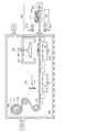
<作製装置の構成例1>
図1(A)に、本発明の一態様の積層体の作製装置を示す。
<Structure example 1 of manufacturing apparatus>
FIG. 1A illustrates a stack body manufacturing apparatus of one embodiment of the present invention.
図1(A)に示す積層体の作製装置20は、第1の支持体供給ユニット190、第1の接
着層形成ユニット110、第1の貼り合わせユニット130、及び制御ユニット150を
有する。
The stacked
第1の支持体供給ユニット190、第1の接着層形成ユニット110、及び第1の貼り合
わせユニット130は、不活性雰囲気にすることができるチャンバー170内に配置され
ていることが好ましい。これにより、積層体を構成する各層を貼り合わせる前に、不純物
等が混入することを抑制できる。さらに、制御ユニット150も、チャンバー170内に
配置されていてもよい。
It is preferable that the first
積層体の作製装置20は、ロールシート状の第1の支持体210rを搬送する複数の搬送
ローラ117を有する。第1の支持体210rの搬送機構に特に限定は無く、搬送ローラ
のほか、ベルトコンベアや搬送ロボットを用いてもよい。
The laminated
第1の支持体供給ユニット190では、ロールシート状の第1の支持体210rを間欠的
に巻き出すことができる。例えば、巻き出しローラ等を用いて、第1の支持体210rを
巻き出すことができる。
In the first
第1の支持体供給ユニット190は、巻き出された第1の支持体210rに張力を加える
ことができる一対の張力付与装置の一方を有する。例えば、ロールシート状の第1の支持
体210rを巻き出すことができるローラ(例えば、図2などに示す巻き出しローラ17
1)が、張力付与装置を有していてもよいし、張力付与装置を兼ねていてもよい。
The first
1) may have a tension applying device or may also serve as a tension applying device.
第1の支持体供給ユニット190は、第1の支持体210rを保管するストック室を有し
ていてもよい。
The first
第1の接着層形成ユニット110では、第1の支持体210r上に第1の接着層219を
形成できる。
In the first adhesive
第1の貼り合わせユニット130では、第1の接着層219を用いて、第1の支持体とシ
ート状の部材211を貼り合わせることができる。貼り合わせ工程は、減圧雰囲気で行わ
れることが好ましいため、第1の貼り合わせユニット130は、減圧雰囲気にすることが
できるチャンバー131を有することが好ましい。
In the
部材211は、ストック室139から供給される。貼り合わせる前の部材211に不純物
が混入しないよう、ストック室139も、不活性雰囲気又は減圧雰囲気にすることができ
ると好ましい。
The
制御ユニット150では、巻き出された第1の支持体210rの端部を保持することがで
きる。制御ユニット150では、第1の支持体210rが巻き出される速度や、一回の巻
き出しで巻き出す量、第1の支持体210rにかける張力等を制御することができる。
The
制御ユニット150は、巻き出された第1の支持体210rに張力を加えることができる
一対の張力付与装置の他方を有する。例えば、ロールシート状の第1の支持体210rの
端部を保持することができる保持機構151が、張力付与装置を有していてもよいし、張
力付与装置を兼ねていてもよい。
The
なお、図1(A)では、保持機構151として第1の支持体210rの幅よりも狭い幅の
保持機構を例示したが、本発明の一態様はこれに限られず、第1の支持体210rの幅以
上の幅の保持機構を用いてもよい。図1(B)では、第1の支持体210rの幅よりも広
い幅の保持機構152を用いる場合を示す。
Note that in FIG. 1A, a holding mechanism having a width narrower than the width of the first supporting
積層体の作製装置20は、分断ユニットを有する。制御ユニット150は、分断ユニット
を兼ねている(制御ユニット150に、分断ユニットが含まれている、ともいえる)。固
定機構157aと固定機構157bの間で第1の支持体210rを分断することができる
。
The laminated
なお、図1(A)では、固定機構157a、bとして、第1の支持体210rの幅よりも
狭い幅の固定機構を例示したが、本発明の一態様はこれに限られず、第1の支持体210
rの幅以上の幅の固定機構を用いてもよい。図1(B)では、第1の支持体210rの幅
よりも広い幅の固定機構156a、bを用いる場合を示す。
Note that in FIG. 1A, a fixing mechanism having a width narrower than the width of the first supporting
A fixing mechanism having a width of r or more may be used. FIG. 1B shows a case where the fixing
なお、制御ユニット150が有する一対の張力付与装置の他方を、固定機構157aが有
していてもよいし、兼ねていてもよい。
The
積層体の作製装置20を用いた積層体の作製工程について、図2〜図4を用いて説明する
。
A manufacturing process of a laminated body using the laminated
図2〜図4に示すように、チャンバー170は、ガス供給機構175と排気機構177を
有する。ガス供給機構175から不活性ガスを供給することで、チャンバー170内を不
活性雰囲気とすることができる。例えば、窒素や希ガス等を供給すればよい。
As shown in FIGS. 2 to 4, the
まず、第1の支持体供給ユニット190で、ロールシート状の第1の支持体210rが、
巻き出しローラ171によって巻き出される。巻き出された第1の支持体210rは、ガ
イドローラ173及び搬送ローラ117によって、各ユニットに送り出される。巻き出し
ローラ171は、第1の支持体210rを間欠的に巻き出すことができる。巻き出されて
いる第1の支持体210rの端部は、制御ユニット150における保持機構151が保持
している。
First, in the first
It is unwound by the unwinding
図2では、第1の支持体供給ユニット190において、第1の支持体210rの巻き出し
を休止している状態の一例を示す。図3では、各ユニットにおける工程が行われている状
態の一例を示す。図4では、第1の支持体供給ユニット190において、第1の支持体2
10rの巻き出しを行っている状態の一例を示す。
FIG. 2 shows an example of a state in which the unwinding of the
An example of a state of unwinding 10r is shown.
第1の支持体210rの巻き出しが停止している状態において、第1の接着層形成ユニッ
ト110では、ステージ113上の第1の支持体210rに第1の接着層219を形成す
る。
In the state where the unwinding of the
ステージ113は、前後、左右、又は上下の少なくともいずれかに移動可能とする。ステ
ージ113上に配置された第1の支持体210rを固定するための固定機構としては、吸
引チャック、静電チャック、メカニカルチャック等のチャックが挙げられる。例えば、ポ
ーラスチャックを用いてもよい。また、吸着テーブル、ヒーターテーブル、スピンナーテ
ーブル等に第1の支持体210rを固定してもよい。
The
第1の接着層219の形成方法に特に限定は無く、例えば、液滴吐出法や、印刷法(スク
リーン印刷法やオフセット印刷法など)、スピンコート法、スプレー塗布法などの塗布法
、ディッピング法、ディスペンス法、ナノインプリント法等を適宜用いることができる。
また、シート状に成形された接着シートを加圧しながら第1の支持体210r上に貼り合
わせてもよい。
The method for forming the first
Alternatively, the adhesive sheet formed into a sheet may be attached to the
接着層形成機構115に特に限定は無く、例えば、印刷装置、ディスペンス装置、塗布装
置、インクジェット装置、スピンコーター、スプレー塗布装置、バーコーター、スリット
コーター等を用いることができる。また、あらかじめシート状に成形された接着シートを
供給する装置を用いてもよい。
The adhesive
第1の接着層219は、後の工程で貼り合わせるシート状の部材211が重なる領域一面
に形成されていてもよいし、縞状などのパターン状に形成されていてもよい。
The first
巻き出しが停止している状態において、第1の貼り合わせユニット130では、第1の接
着層219を用いて、ステージ133上の第1の支持体210rにシート状の部材211
を貼り合わせる。これにより、第1の支持体210r、第1の接着層219、及び部材2
11を有する第1の積層体220を作製することができる。
In the state where the unwinding is stopped, in the
Stick together. Thereby, the
A
第1の貼り合わせユニット130では、第1の支持体210rの巻き出しが休止した後、
チャンバー131内を減圧雰囲気とする。その後、減圧雰囲気のストック室139からシ
ート状の部材211が供給される。
In the
The inside of the
チャンバー131内を減圧雰囲気とすることで、貼り合わせ時に、不純物や気泡等が、第
1の支持体210r、第1の接着層219、及び部材211の間に混入することを抑制で
きる。また、ストック室139内を減圧雰囲気とすることで、貼り合わせる前の部材21
1に不純物が混入することを抑制できる。
By setting the reduced pressure atmosphere in the
It is possible to prevent impurities from being mixed into 1.
ステージ133は、前後、左右、又は上下の少なくともいずれかに移動可能とする。ステ
ージ133上に配置された第1の支持体210rを固定するための固定機構としては、ス
テージ113と同様の構成が挙げられる。
The
部材保持機構135は、供給されたシート状の部材211を保持する。例えば、各ステー
ジと同様の構成で部材211を固定することができる。
The
部材保持機構135を用いて、部材211の貼り合わせる面全体を加圧しながら、部材2
11と第1の支持体210rを貼り合わせることで、部材211と第1の支持体210r
の間に気泡が混入することを抑制できる。また、第1の接着層219の膜厚が不均一にな
ることを抑制できる。また、部材211と第1の支持体210rは、一の端部から貼り合
わせてもよい。
The
11 and the
It is possible to prevent bubbles from being mixed in between. Further, it is possible to prevent the film thickness of the first
加圧時に、第1の接着層219が、未硬化状態、半硬化状態等の、流動性を有する状態で
あると、気泡の混入や膜厚のばらつきをより抑制できる。また、加圧時に、第1の接着層
219は接着性(粘着性)を有していてもよいし、加圧後に接着性を発現させてもよい。
When the first
第1の接着層219の材料が部材211と第1の支持体210rの端部をはみ出してステ
ージ133上等に付着しないことが好ましい。第1の接着層219のパターンや材料の量
によって適宜制御すればよい。また、ステージ133上等に付着した第1の接着層219
の材料をふきとる機構を第1の貼り合わせユニット130が有していてもよい。例えば、
アセトン等の有機溶剤や、布等のワイパーを用いてもよい。
It is preferable that the material of the first
The
An organic solvent such as acetone or a wiper such as cloth may be used.
部材保持機構135がヒータ等の加熱機構を有していてもよい。第1の接着層219に熱
硬化型の接着剤を用いた場合、該加熱機構によって、貼り合わせと同時に接着剤を硬化す
ることができ、好ましい。
The
また、積層体の作製装置において、第1の積層体が供給され、第1の接着層を硬化させる
ことができる第1の接着層硬化ユニットを有していてもよい。例えば、第1の貼り合わせ
ユニット130と制御ユニット150の間に、第1の接着層硬化ユニットを有していても
よい。接着層硬化ユニットは、熱硬化型の接着剤を硬化させるための加熱機構(ヒータ等
の熱源)や、光硬化型の接着剤を硬化させるための光照射機構(レーザ、ランプ等の光源
)を有していればよい。
Further, the laminated body manufacturing apparatus may include a first adhesive layer curing unit which is supplied with the first laminated body and can cure the first adhesive layer. For example, a first adhesive layer curing unit may be provided between the
図2〜図4では、制御ユニット150に分断ユニットが含まれる場合を説明する。巻き出
しが停止している状態において、分断ユニットでは、分断機構155を用いて第1の支持
体210rを分断する。
2 to 4, a case where the
分断ユニットは、固定機構157aと固定機構157bの間で第1の支持体210rを分
断することができる。
The dividing unit can divide the
ステージ153は、前後、左右、又は上下の少なくともいずれかに移動可能とする。ステ
ージ153上に配置された第1の支持体210rを固定するための固定機構としては、ス
テージ113と同様の構成が挙げられる。
The
分断機構155としては、第1の支持体210rを分断できるものであれば特に限定はな
く、カッター等の鋭利な刃物や、レーザ等を用いればよい。
The
固定機構157a、bは、第1の支持体210rを固定できれば特に限定は無く、例えば
、クリップ等を用いてもよい。固定機構157a、bは、第1の支持体210rを送り出
すことができる。例えば、固定機構157a、bは、前後、左右、又は上下の少なくとも
いずれかに移動可能とすることが好ましい。
The
固定機構157aは、第1の支持体210rに張力を加えることができる一対の張力付与
装置の他方を有する。第1の支持体210rが分断された後、チャンバー170内の第1
の支持体210rは固定機構157a及び巻き出しローラ171が有する一対の張力付与
装置によって張力が与えられ、静止した状態を保つことができる。また、チャンバー17
0の外の第1の支持体210rは、ステージ153、固定機構157b、及び保持機構1
51によって支持される。
The
The supporting
The
Supported by 51.
固定機構157aと巻き出しローラ171でチャンバー170内の第1の支持体210r
に張力を与え続けられる場合、保持機構151は、張力付与装置を有していなくてもよい
。
The
When the tension can be continuously applied to the
図3に示すように、第1の支持体210rが分断された後、ステージ153、固定機構1
57b、及び保持機構151が移動し、チャンバー170の外の第1の支持体210rか
ら離れる。これにより、第1の支持体210、第1の接着層219、及び部材211を有
する第1の積層体250を、積層体の作製装置20内から取り出すことができる。積層体
の作製装置20は、搬出機構や、搬出ユニットを有していてもよい。
As shown in FIG. 3, after the
57b and the
次に、保持機構151が移動し、固定機構157aが保持する第1の支持体210rの端
部を挟持する。
Next, the
そして、図4に示すように、固定機構157a、ステージ113、ステージ133、及び
チャンバー131が移動し、第1の支持体210rから離れる。その後、第1の支持体2
10rが巻き出しが再開され、搬送ローラ117上を搬送される。第1の支持体210r
が一定量巻き出された後は、巻き出しが停止する。そして、図2の状態に戻り、各ユニッ
トにおいて、積層体の作製に係る各工程が行われる。
Then, as shown in FIG. 4, the
The unwinding of 10r is resumed, and the sheet 10r is conveyed on the conveying
After being unwound by a certain amount, unwinding stops. Then, returning to the state of FIG. 2, in each unit, each step relating to the production of the laminated body is performed.
<作製装置の変形例>
図1(A)、及び図2〜図4では、積層体の作製装置20が、分断ユニットを有する例を
示したが、本発明の一態様はこれに限られない。図5(A)に示すように、制御ユニット
150が巻き取りユニットを兼ねて(制御ユニット150に、巻き取りユニットが含まれ
て)いてもよい。
<Modification of manufacturing device>
Although FIG. 1A and FIGS. 2 to 4 show an example in which the
図5(A)に示す制御ユニット150では、巻き出された第1の支持体210rに張力を
加えることができる一対の張力付与装置の他方として、巻き取りローラ178を有する場
合を示す。巻き取りローラ178は、巻き出された第1の支持体210rの端部を保持す
ることができる。巻き取りローラ178は、ロールシート状の第1の積層体220rを巻
き取ることができる。
In the
図5(B)にロールシート状の第1の積層体220rを展開した状態を示す。第1の積層
体220rは、第1の積層体220を複数有する。第1の積層体220は、第1の支持体
210r、第1の接着層219、及び部材211を有する。つまり、ロールシート状の第
1の積層体220rは、第1の支持体210r上に、第1の接着層219を用いて貼り合
わされた部材211を複数有する。
FIG. 5B shows a developed state of the roll sheet-shaped first
第1の積層体220rは、複数の搬送ローラ117及びガイドローラ179を介して巻き
取りローラ178に巻き取られる。
The first
また、図5(A)に示すように、第1の接着層形成ユニット110は、減圧雰囲気にする
ことができるチャンバー111を有していてもよい。例えば、第1の接着層219の材料
として、シート状に成形された接着シートを用いる場合、第1の支持体210r上に接着
シートを貼り合わせる際に減圧雰囲気とすることで、気泡等の混入を抑制できる。また、
加圧ローラ112等の加圧機構を用いることでも、気泡等の混入を抑制でき、好ましい。
Further, as shown in FIG. 5A, the first adhesive
The use of a pressure mechanism such as the
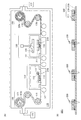
<作製装置の構成例2>
図1(B)に、本発明の別の態様の積層体の作製装置を示す。なお、構成例1と同様の構
成については、説明を省略する。
<Structure example 2 of manufacturing apparatus>
FIG. 1B shows a stack manufacturing apparatus of another embodiment of the present invention. The description of the same configuration as the configuration example 1 is omitted.
図1(B)に示す積層体の作製装置21は、第1の支持体供給ユニット190、第1の接
着層形成ユニット110、第1の貼り合わせユニット130、起点形成ユニット120、
分離ユニット140、第2の接着層形成ユニット160、第2の貼り合わせユニット18
0、及び制御ユニット150を有する。
The laminated
0, and a
第1の支持体供給ユニット190、第1の接着層形成ユニット110、及び第1の貼り合
わせユニット130は、不活性雰囲気にすることができるチャンバー170内に配置され
ていることが好ましい。さらに、起点形成ユニット120、分離ユニット140、第2の
接着層形成ユニット160、第2の貼り合わせユニット180、及び制御ユニット150
も、チャンバー170内に配置されていてもよい。
It is preferable that the first
Alternatively, it may be arranged in the
積層体の作製装置21は、ロールシート状の第1の支持体210rを搬送する複数の搬送
ローラ117を有する。
The laminated
第1の支持体供給ユニット190、第1の接着層形成ユニット110、第1の貼り合わせ
ユニット130、及び制御ユニット150は、積層体の作製装置20と同様であるため、
説明を省略する。
The first
The description is omitted.
起点形成ユニット120では、第1の貼り合わせユニット130から供給される第1の積
層体220に剥離の起点を形成することができる。
In the starting
分離ユニット140では、剥離の起点が形成された第1の積層体220を、表層222と
残部221とに分離することができる。表層222はストック室149に収納される。
In the
第2の接着層形成ユニット160では、残部221上に第2の接着層229を形成するこ
とができる。
In the second adhesive
第2の貼り合わせユニット180では、第2の接着層229を用いて、残部221と第2
の支持体231rを貼り合わせることができる。貼り合わせ工程は、減圧雰囲気で行われ
ることが好ましいため、第2の貼り合わせユニット180は、減圧雰囲気にすることがで
きるチャンバー181を有することが好ましい。
In the
The
第2の支持体231rは、チャンバー181に配置されていてもよい。第2の支持体23
1rは、チャンバー181と接続するストック室189から供給されてもよい。貼り合わ
せる前の第2の支持体231rに不純物が混入しないよう、ストック室189も、不活性
雰囲気又は減圧雰囲気にすることができると好ましい。
The
1r may be supplied from a
積層体の作製装置21を用いた積層体の作製工程について、図6及び図7(A)を用いて
説明する。なお、第1の支持体供給ユニット190、第1の接着層形成ユニット110、
第1の貼り合わせユニット130における工程は、積層体の作製装置20と同様であるた
め、説明を省略する。
A manufacturing process of a stack using the
Since the steps in the
図6及び図7(A)では、第1の支持体供給ユニット190において、第1の支持体21
0rの巻き出しを休止している期間における、起点形成ユニット120、分離ユニット1
40、第2の接着層形成ユニット160、第2の貼り合わせユニット180、及び制御ユ
ニット150の一例を示す。
In FIG. 6 and FIG. 7A, in the first
The starting
40 shows an example of the second adhesive
図6に示すように、第1の支持体210rの巻き出しが停止している状態において、起点
形成ユニット120では、ステージ123上の第1の積層体220に剥離の起点を形成す
る。
As shown in FIG. 6, in the state where the unwinding of the
起点形成機構としては、例えば、カッター等の鋭利な刃物や、レーザを用いることができ
る。
As the starting point forming mechanism, for example, a sharp blade such as a cutter or a laser can be used.
ここでは、一例として、起点形成ユニット120がレーザ照射システムを有する場合につ
いて説明する。
Here, as an example, a case where the starting
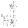
起点形成ユニット120が有するレーザ照射システムは、ステージ123、処理部505
、表示装置507、カメラ509、レーザ装置511、位置合わせ機構(図示しない)、
及び光源515を有する。
The laser irradiation system included in the starting
,
And a
表示装置507には、処理部505を介してカメラ509の観察結果が出力される。
The observation result of the
カメラ509には、例えば、カメラを含む光学顕微鏡等を用いることができる。カメラ5
09で検出された光は、処理部505で処理され、画像として表示装置507に表示され
る。
As the
The light detected in 09 is processed by the
レーザ装置511は、剥離の起点を形成するためのレーザ光を照射することができる装置
である。
The
処理部505は、表示装置507、カメラ509、レーザ装置511、位置合わせ機構、
及び光源515と接続されている。本実施の形態のレーザ照射システムは、処理部505
を有するため、カメラ509の観察結果等に応じて、自動で、位置合わせ機構やレーザ装
置511、光源515を動作させる設定とすることができる。また、表示装置507に出
力されるカメラ509の観察結果等に応じて、実施者が適宜、位置合わせ機構やレーザ装
置511、光源515を動作させることもできる。
The
And a
Therefore, the position adjustment mechanism, the
ここでは、カメラ509によって、レーザ光照射位置593を直接検出する場合を例に挙
げて説明するが、第1の積層体220におけるレーザ光照射位置593を、マーカ位置か
らの距離によって設定し、該マーカ位置を検出することで、レーザ光照射位置を決定して
もよい。
Here, the case where the laser
可動式のハーフミラー517の向きを変えることで、第1の積層体220に光源515か
らの光535、又はレーザ光531を照射することができる。
By changing the direction of the
はじめに、シャッター521aを開き、位置合わせ機構を用いてステージ123を動かし
ながら、カメラ509によって光を検出する。光源515からの光535は、シャッター
521cが開くと、ハーフミラー517及び集光レンズ523を介して第1の積層体22
0に照射される。第1の積層体220からの反射光533が集光レンズ523及びハーフ
ミラー517を介してカメラ509に照射される。これによって、第1の積層体220に
おけるレーザ光照射位置593を特定する。このとき、シャッター521bは閉じている
。
First, the
It is irradiated to 0. The reflected light 533 from the first
続いて、シャッター521a、cを閉じ、ハーフミラー517の向きを変え、シャッター
521bを開いて、レーザ装置511からレーザ光531を発振する。レーザ光531は
、ハーフミラー517、集光レンズ523を介して、第1の積層体220におけるレーザ
光照射位置593に照射される。これにより、剥離の起点を第1の積層体220に形成す
ることができる。
Subsequently, the
図6に示すように、第1の支持体210rの巻き出しが停止している状態において、分離
ユニット140では、第1の積層体220を、表層222及び残部221に分離する。具
体的には、剥離の起点を用いて、ステージ143上の第1の積層体220から表層222
を剥離することで、表層222及び残部221に分離できる。
As shown in FIG. 6, in the state where the unwinding of the
Can be separated into the
例えば、吸着パッドなどの吸着部材147を用いて表層222を剥離すればよい。
For example, the
分離ユニット140は、剥離したい界面に差し込む鋭利な刃物145を有していてもよい
。刃物を差し込むことで、剥離を円滑に開始できる。
The
また、分離ユニット140は、剥離の進行部に液体を供給するノズルを有していてもよい
。剥離の進行部に水等の液体を供給することで、剥離強度を低下させることができる。ま
た、第1の積層体220に含まれる素子の静電破壊を抑制できる。
In addition, the
図7(A)に示すように、第1の支持体210rの巻き出しが停止している状態において
、第2の接着層形成ユニット160では、ステージ163上の残部221に第2の接着層
229を形成する。
As shown in FIG. 7A, in the state where the unwinding of the
第2の接着層形成ユニット160は、第1の接着層形成ユニット110と同様の構成を適
用できる。ここでは、接着層形成機構165として、接着層形成機構115と同様の構成
を用いる例を示すが、第2の接着層形成ユニット160は、第1の接着層形成ユニット1
10とは異なる形成機構及び異なる形成方法を適用してもよい。
The second adhesive
A forming mechanism different from 10 and a different forming method may be applied.
巻き出しが停止している状態において、第2の貼り合わせユニット180では、第2の接
着層229を用いて、ステージ183上の残部221に第2の支持体231rを貼り合わ
せる。これにより、残部221、第2の接着層229、及び第2の支持体231rを有す
る第2の積層体223を作製することができる。
In the state where the unwinding is stopped, in the
第2の貼り合わせユニット180では、第1の支持体210rの巻き出しを休止した後、
チャンバー181内を減圧雰囲気とする。チャンバー181内を減圧雰囲気とすることで
、貼り合わせ時に、不純物や気泡等が、残部221、第2の接着層229、及び第2の支
持体231rの間に混入することを抑制できる。
In the
The pressure inside the
ステージ183は、前後、左右、又は上下の少なくともいずれかに移動可能とする。ステ
ージ183上に配置された第1の支持体210rを固定するための固定機構としては、ス
テージ113と同様の構成が挙げられる。
The
ここでは、ロールシート状の第2の支持体231rを用いる例を示すが、第2の支持体は
これに限られない。例えば、シート状の第2の支持体を用いてもよい。
Here, an example using the roll sheet-shaped
巻き出しローラ185は、第2の支持体231rを間欠的に巻き出すことができる。巻き
出されている第2の支持体231rの端部は、制御ユニット150における保持機構15
2が保持していてもよい。また、別の保持機構によって保持されていてもよい。
The unwinding
2 may hold. Further, it may be held by another holding mechanism.
巻き取りローラ188は、分離テープ233を間欠的に巻き取ることができる。
The take-up
保持機構152が第2の支持体231rの端部を保持している場合、第1の支持体210
rと第2の支持体231rの巻き出しは同時に行うことができる。第1の支持体210r
と第2の支持体231rの端部が異なる保持機構によって固定されている場合、第1の支
持体210rと第2の支持体231rの巻き出しはそれぞれ独立に行うことができる。
When the
The unwinding of r and the
When the end portions of the
まず、ロールシート状の第2の支持体231rが、巻き出しローラ185によって巻き出
される。巻き出された第2の支持体231rは、ガイドローラ184によって送り出され
る。そして、第2の支持体231rから分離テープ233(セパレートフィルムとも呼ば
れる)を、巻き取りローラ188で引っ張り剥離する。
First, the roll sheet-shaped
第2の支持体231rの、第2の接着層229と貼り合わせる面が、貼り合わせる直前に
露出することで、第2の支持体231rの巻き出し中にゴミやキズがつくことを抑制でき
る。
By exposing the surface of the
第2の支持体231rから剥離した分離テープ233は、ガイドローラ187を介して、
巻き取りローラ188に巻き取られる。分離テープ233が剥離された第2の支持体23
1rは、方向転換ローラ186により、第1の支持体210rの搬送方向とほぼ同一方向
に送り出される。
The
It is taken up by the take-up
The
静電気が発生する恐れのある位置には、イオナイザ191を設け、イオナイザからエア又
は窒素ガス等を吹き付け除電処理を行ってもよい。
An
加圧ローラ182を用いて、第2の支持体231rの貼り合わせる面を加圧しながら、残
部221と第2の支持体231rを貼り合わせることで、残部221と第2の支持体23
1rの間に気泡が混入することを抑制できる。また、第2の接着層229の膜厚が不均一
になることを抑制できる。
The remaining
It is possible to prevent bubbles from being mixed in during 1r. Further, it is possible to prevent the film thickness of the second
加圧ローラ182が、ヒータ等の加熱機構を有していてもよい。第2の接着層229に熱
硬化型の接着剤を用いた場合、該加熱機構によって、貼り合わせと同時に接着剤を硬化す
ることができ、好ましい。
The
また、積層体の作製装置において、第2の積層体が供給され、第2の接着層を硬化させる
ことができる第2の接着層硬化ユニットを有していてもよい。例えば、第2の貼り合わせ
ユニット180と制御ユニット150の間に、第2の接着層硬化ユニットを有していても
よい。
Further, the apparatus for manufacturing a laminated body may have a second adhesive layer curing unit which is supplied with the second laminated body and can cure the second adhesive layer. For example, a second adhesive layer curing unit may be provided between the
第1の支持体210rの巻き出しが停止している状態において、分断ユニットでは、分断
機構155を用いて第1の支持体210r及び第2の支持体231rを分断する。
When the unwinding of the
分断ユニットは、固定機構156aと固定機構156bの間で第1の支持体210rを分
断することができる。
The dividing unit can divide the
固定機構156a、bは、第1の支持体210rを固定できれば特に限定は無く、例えば
、クリップ等を用いてもよい。固定機構156a、bは、前後、左右、又は上下の少なく
ともいずれかに移動可能とする。
The
図1(B)及び図7(A)では、積層体の作製装置21が、分断ユニットを有する例を示
したが、制御ユニット150が巻き取りユニットを兼ねて(制御ユニット150に、巻き
取りユニットが含まれて)いてもよい。
In FIG. 1B and FIG. 7A, the example in which the laminated
図7(B)に巻き取りユニットが巻き取ることができる、ロールシート状の第2の積層体
223rを展開した状態を示す。第2の積層体223rは、第2の積層体223を複数有
する。第2の積層体223は、残部221、第2の接着層229、及び第2の支持体23
1rを有する。つまり、ロールシート状の第2の積層体223rは、第1の支持体210
r上に、第1の接着層219を用いて貼り合わされた部材211の一部と、該部材211
の一部上に第2の接着層229を用いて貼り合わされた第2の支持体231rと、を複数
有する。
FIG. 7B shows a state in which the roll-sheet-shaped second
Has 1r. That is, the roll-sheet-shaped second
and a part of the
A plurality of
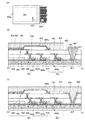
<積層体の構成例>
上記本発明の一態様の作製装置を用いて作製できる積層体の構成の一例について図8を用
いて説明する。
<Structure example of laminated body>
An example of a structure of a stack which can be manufactured using the manufacturing apparatus of one embodiment of the present invention will be described with reference to FIGS.
図8(A)に示す積層体は、一対のガスバリア性の高い層200の間に素子層201を有
する。素子層201の上下にガスバリア性の高い層200を設けることで、素子層201
に含まれる機能素子が水分等の不純物によって劣化することを抑制することができる。
The stacked body illustrated in FIG. 8A includes an
It is possible to prevent the functional element included in the element from being deteriorated by impurities such as moisture.
図8(B)に示す積層体は、図1(A)の積層体の作製装置20を用いて作製できる。例
えば、まず、ロールシート状のガスバリア性の高い層200を、第1の支持体供給ユニッ
ト190から供給し、第1の接着層形成ユニット110で接着層209を形成する。次に
、素子層201が形成されたシート状のガスバリア性の高い層200を、第1の貼り合わ
せユニット130に供給し、接着層209を用いて、ロールシート状のガスバリア性の高
い層200と貼り合わせる。これにより、図8(B)に示す積層体を作製できる。
The stacked body illustrated in FIG. 8B can be manufactured using the
また、本発明の一態様の積層体の作製装置は、機能素子形成ユニットを有していてもよい
。例えば、ロールシート状のガスバリア性の高い層200を、第1の支持体供給ユニット
190から供給し、機能素子形成ユニットで、素子層201を形成する。次に、第1の接
着層形成ユニット110で素子層201上に接着層209を形成する。そして、シート状
のガスバリア性の高い層200を、第1の貼り合わせユニット130に供給し、接着層2
09を用いて、素子層201と貼り合わせる。これにより、図8(B)に示す積層体を作
製できる。
Further, the stack manufacturing apparatus of one embodiment of the present invention may include a functional element formation unit. For example, a roll sheet-
09, and is attached to the
図8(C)に示す積層体は、図1(B)の積層体の作製装置21を用いて作製できる。例
えば、まず、耐熱性の高い作製基板上に剥離層(実施の形態2参照)を介して素子層20
1を作製する。これをシート状の部材211とする。そして、積層体の作製装置21にお
いて、ロールシート状のガスバリア性の高い層200を、第1の支持体供給ユニット19
0から供給し、第1の接着層形成ユニット110で接着層209を形成する。次に、素子
層201を含むシート状の部材211を、第1の貼り合わせユニット130に供給し、接
着層209を用いて、ロールシート状のガスバリア性の高い層200と貼り合わせる。次
に、起点形成ユニット120にて、シート状の部材211に剥離の起点を形成する。剥離
の起点が形成されたシート状の部材211を、分離ユニット140にて、表層222と、
残部(素子層201)に分離する。次に、第2の接着層形成ユニット160で素子層20
1上に接着層209を形成する。そして、シート状のガスバリア性の高い層200を、第
2の貼り合わせユニット180に供給し、接着層209を用いて、素子層201と貼り合
わせる。これにより、図8(C)に示す積層体を作製できる。
The stacked body illustrated in FIG. 8C can be manufactured using the
1 is produced. This is a sheet-shaped
Then, the
The rest (element layer 201) is separated. Next, the
An
上記積層体の作製方法では、積層体を構成するガスバリア性の高い層200とは異なる作
製基板上で素子層201を形成することができる。したがって、素子層201の形成方法
が、ガスバリア性の高い層200の材料によって制限されないため、好ましい。例えば、
耐熱性が低く、ガスバリア性の高い材料を用いることができる。
In the above method for manufacturing a stacked body, the
A material having low heat resistance and high gas barrier properties can be used.
図8(D)に示すように、ガスバリア性の高い層200は積層構造であってもよく、接着
層203を用いてガスバリア性の低い層204とガスバリア性の高い層202が貼り合わ
された構造であってもよい。
As shown in FIG. 8D, the
図8(D)に示す積層体は、図1(B)の積層体の作製装置21を用いて作製できる。例
えば、まず、耐熱性の高い作製基板上に剥離層を介してガスバリア性の高い層202及び
素子層201をこの順で作製する。これをシート状の部材211とする。そして、ロール
シート状のガスバリア性の高い層200を、第1の支持体供給ユニット190から供給し
、第1の接着層形成ユニット110で接着層209を形成する。次に、ガスバリア性の高
い層202及び素子層201を含むシート状の部材211を、第1の貼り合わせユニット
130に供給し、接着層209を用いて、ロールシート状のガスバリア性の高い層200
と貼り合わせる。次に、起点形成ユニット120にて、シート状の部材211に剥離の起
点を形成する。剥離の起点が形成されたシート状の部材211を、分離ユニット140に
て、表層222と、残部(ガスバリア性の高い層202及び素子層201)に分離する。
そして、第2の接着層形成ユニット160でガスバリア性の高い層202上に接着層20
3を形成する。シート状のガスバリア性の低い層204を、第2の貼り合わせユニット1
80に供給し、接着層203を用いて、ガスバリア性の高い層202と貼り合わせる。こ
れにより、図8(D)に示す積層体を作製できる。
The stacked body illustrated in FIG. 8D can be manufactured using the
And paste. Next, the starting
Then, in the second adhesive
3 is formed. The sheet-shaped
80, and is bonded to the
上記積層体の作製方法では、積層体を構成するガスバリア性の高い層200や、ガスバリ
ア性の低い層204とは異なる作製基板上で素子層201を形成することができる。した
がって、素子層201の形成方法が、ガスバリア性の高い層200や、ガスバリア性の低
い層204の材料によって制限されないため、好ましい。例えば、耐熱性の高い作製基板
上で、素子層201やガスバリア性の高い層202を形成することができる。
In the above method for manufacturing a stacked body, the
図8(E)に示す積層体の作製方法としては、例えば、まず、ロールシート状のガスバリ
ア性の高い層200を、第1の支持体供給ユニット190から供給し、機能素子形成ユニ
ットで、素子層201を形成する。そして、第1の接着層形成ユニット110で素子層2
01上に接着層209を形成する。ガスバリア性の高い層202を含むシート状の部材2
11を、第1の貼り合わせユニット130に供給し、接着層209を用いて、素子層20
1と貼り合わせる。次に、起点形成ユニット120にて、シート状の部材211に剥離の
起点を形成する。剥離の起点が形成されたシート状の部材211を、分離ユニット140
にて、表層222と、残部(ガスバリア性の高い層202)に分離する。そして、第2の
接着層形成ユニット160でガスバリア性の高い層202上に接着層203を形成する。
シート状のガスバリア性の低い層204を、第2の貼り合わせユニット180に供給し、
接着層203を用いて、ガスバリア性の高い層202と貼り合わせる。これにより、図8
(E)に示す積層体を作製できる。
As a method for manufacturing the stacked body illustrated in FIG. 8E, for example, first, a roll sheet-
The
11 is supplied to the
Stick with 1. Next, the starting
At, the
The sheet-shaped
The
The laminate shown in (E) can be produced.
また、本発明の一態様の積層体の作製装置は、各ユニットを複数有していてもよい。例え
ば、起点形成ユニットや分離ユニットを複数有していてもよい。
Further, the stack manufacturing apparatus of one embodiment of the present invention may include a plurality of each unit. For example, it may have a plurality of starting point forming units and separation units.
図8(F)に示す積層体の作製方法としては、例えば、ロールシート状のガスバリア性の
低い層204を、第1の支持体供給ユニット190から供給し、第1の接着層形成ユニッ
ト110で接着層203を形成する。ガスバリア性の高い層202を含むシート状の部材
211を、第1の貼り合わせユニット130に供給し、接着層203を用いて、ロールシ
ート状のガスバリア性の低い層204と貼り合わせる。次に、起点形成ユニット120に
て、シート状の部材211に剥離の起点を形成する。剥離の起点が形成されたシート状の
部材211を、分離ユニット140にて、表層222と、残部(ガスバリア性の高い層2
02)に分離する。そして、第2の接着層形成ユニット160でガスバリア性の高い層2
02上に接着層209を形成する。そして、ガスバリア性の高い層202及び素子層20
1を含むシート状の部材を、第2の貼り合わせユニット180に供給し、接着層209を
用いて、ガスバリア性の高い層202と貼り合わせる。次に、第2の起点形成ユニットに
て、シート状の部材に剥離の起点を形成する。剥離の起点が形成されたシート状の部材を
、第2の分離ユニットにて、表層と、残部(ガスバリア性の高い層202及び素子層20
1)に分離する。そして、第3の接着層形成ユニットでガスバリア性の高い層202上に
接着層203を形成する。シート状のガスバリア性の低い層204を、第3の貼り合わせ
ユニットに供給し、接着層203を用いて、ガスバリア性の高い層202と貼り合わせる
。これにより、図8(F)に示す積層体を作製できる。
As a method for manufacturing the stacked body illustrated in FIG. 8F, for example, a roll sheet-shaped
02). Then, in the second adhesive
An
A sheet-shaped member containing 1 is supplied to the
Separate into 1). Then, the third adhesive layer forming unit forms the
以上に示したように、本発明の一態様の積層体の作製装置を用いて、素子層が一対のバリ
ア性の高い層に挟持された信頼性の高い積層体(又は装置)を作製することができる。な
お、各層に可撓性を有する材料を用いることで、可撓性を有する積層体(又はフレキシブ
ルデバイス)を作製することができる。
As described above, with the use of the stack manufacturing apparatus of one embodiment of the present invention, a highly reliable stack (or a device) in which an element layer is sandwiched between a pair of layers with high barrier properties is manufactured. You can Note that a flexible laminate (or a flexible device) can be manufactured by using a flexible material for each layer.
本実施の形態は、他の実施の形態と適宜組み合わせることができる。 This embodiment can be combined with any of the other embodiments as appropriate.
(実施の形態2)
本実施の形態では、本発明の一態様を適用して作製できるフレキシブルな発光パネルにつ
いて、図9〜図12を用いて説明する。
(Embodiment 2)
In this embodiment, a flexible light-emitting panel that can be manufactured by applying one embodiment of the present invention will be described with reference to FIGS.
本実施の形態の発光パネルは、発光素子として有機EL素子を有する。一対のバリア層の
間に該有機EL素子を有するため、本実施の形態の発光パネルは、信頼性が高い。なお、
本明細書中において、バリア性の高い層をバリア層とも記す。
The light-emitting panel of this embodiment has an organic EL element as a light-emitting element. Since the organic EL element is provided between the pair of barrier layers, the light emitting panel of this embodiment has high reliability. In addition,
In this specification, a layer having a high barrier property is also referred to as a barrier layer.
一対のバリア層の少なくとも一方は有機EL素子の発光を透過する。本実施の形態の発光
パネルには、トップエミッション構造の有機EL素子を用いてもよいし、ボトムエミッシ
ョン構造の有機EL素子を用いてもよいし、デュアルエミッション構造の有機EL素子を
用いてもよい。
At least one of the pair of barrier layers transmits light emitted from the organic EL element. For the light-emitting panel of this embodiment, a top-emission structure organic EL element, a bottom-emission structure organic EL element, or a dual-emission structure organic EL element may be used. ..
本発明の一態様では、パッシブマトリクス方式の発光パネルと、トランジスタによって発
光素子の駆動が制御されたアクティブマトリクス方式の発光パネルと、のいずれも作製す
ることができる。
According to one embodiment of the present invention, both a passive matrix light-emitting panel and an active matrix light-emitting panel in which driving of a light-emitting element is controlled by a transistor can be manufactured.
<発光パネルの構成例1>
図9(A)に発光パネルの平面図を示し、図9(B)に、図9(A)の一点鎖線X1−Y
1間及びX2−Y2間の断面図を示す。
<Configuration example 1 of light emitting panel>
9A shows a plan view of the light-emitting panel, and FIG. 9B shows a dashed-dotted line X1-Y in FIG. 9A.
The cross section between 1 and X2-Y2 is shown.
図9(B)に示す発光パネルは、バリア層490b、導電層406、導電層416、絶縁
層405、有機EL素子450(第1の電極401、EL層402、及び第2の電極40
3)、接着層407、及びバリア層490aを有する。
In the light-emitting panel illustrated in FIG. 9B, the
3), the
構成例1では、バリア層490aは、バリア性の高い可撓性基板からなり、バリア層49
0bは、可撓性基板420b、接着層422b、及びバリア性の高い絶縁層424bから
なる例を示す。
In Configuration Example 1, the
0b indicates an example including a
有機EL素子450は、バリア層490a上の第1の電極401と、第1の電極401上
のEL層402と、EL層402上の第2の電極403とを有する。バリア層490a、
接着層407、及びバリア層490bによって、有機EL素子450は封止されている。
The
The
第1の電極401、導電層406、導電層416の端部は絶縁層405で覆われている。
導電層406は第1の電極401と電気的に接続し、導電層416は第2の電極403と
電気的に接続する。第1の電極401を介して絶縁層405に覆われた導電層406は、
補助配線として機能し、第1の電極401と電気的に接続する。有機EL素子の電極と電
気的に接続する補助配線を有すると、電極の抵抗に起因する電圧降下を抑制できるため、
好ましい。導電層406は、第1の電極401上に設けられていてもよい。また、絶縁層
405上等に、第2の電極403と電気的に接続する補助配線を有していてもよい。
The end portions of the
The
It functions as an auxiliary wiring and is electrically connected to the
preferable. The
発光パネルの光取出し効率を高めるため、発光素子からの光を取り出す側に光取り出し構
造を有していてもよい。
In order to improve the light extraction efficiency of the light emitting panel, a light extraction structure may be provided on the side where the light from the light emitting element is extracted.
以下に、構成例1の発光パネルの作製方法の一例を示す。構成例1の発光パネルは、図1
(B)に示す積層体の作製装置21を用いて作製できる。
An example of a method for manufacturing the light-emitting panel of Structural Example 1 is shown below. The light emitting panel of the configuration example 1 is shown in FIG.
It can be manufactured using the
例えば、まず、耐熱性の高い作製基板上に剥離層を形成する。次に、剥離層上に被剥離層
として、バリア性の高い絶縁層424bから有機EL素子450までを形成する。これが
、シート状の部材211に相当する。
For example, first, a peeling layer is formed over a manufacturing substrate having high heat resistance. Next, the insulating
第1の支持体供給ユニット190では、ロールシート状のバリア層490aを供給する。
第1の接着層形成ユニット110では、ロールシート状のバリア層490a上に接着層4
07を形成する。第1の貼り合わせユニット130では、接着層407を用いてシート状
の部材211とバリア層490aを貼り合わせる。起点形成ユニット120では、部材2
11に剥離の起点を形成する。分離ユニット140では、剥離の起点を形成した部材21
1を表層(作製基板及び剥離層)と残部(バリア性の高い絶縁層424bから有機EL素
子450まで)に分離する。第2の接着層形成ユニット160では、バリア性の高い絶縁
層424b上に接着層422bを形成する。第2の貼り合わせユニット180では、接着
層422bを用いてバリア性の高い絶縁層424bとロールシート状の可撓性基板420
bとを貼り合わせる。
In the first
In the first adhesive
07 is formed. In the
The starting point of peeling is formed at 11. In the
1 is separated into a surface layer (fabrication substrate and peeling layer) and the rest (from the insulating
Stick with b.
または、有機EL素子の形成ユニットを有する積層体の作製装置を用いてもよい。例えば
、耐熱性の高い作製基板上に剥離層を介して形成したバリア性の高い絶縁層424bを、
ロールシート状の可撓性基板420b上に接着層422bを用いて転置する。次に、バリ
ア性の高い絶縁層424b上に、有機EL素子450を形成し、その後、接着層407を
用いて有機EL素子450とロールシート状のバリア層490aとを貼り合わせる。
Alternatively, a stacked body manufacturing apparatus including an organic EL element formation unit may be used. For example, an insulating
The
<発光パネルの構成例2>
図9(A)に発光パネルの平面図を示し、図9(C)に、図9(A)の一点鎖線X1−Y
1間及びX2−Y2間の断面図を示す。なお、構成例1と同様の構成については説明を省
略する。
<Configuration example 2 of light emitting panel>
9A shows a plan view of the light-emitting panel, and FIG. 9C shows a dashed-dotted line X1-Y in FIG. 9A.
The cross section between 1 and X2-Y2 is shown. Note that the description of the same configuration as the configuration example 1 is omitted.
図9(C)に示す発光パネルは、バリア層490a、導電層406、導電層416、絶縁
層405、有機EL素子450、接着層407、及びバリア層490bを有する。
The light-emitting panel illustrated in FIG. 9C includes a
構成例2では、バリア層490aは、バリア性の高い可撓性基板からなり、バリア層49
0bは、可撓性基板420b、接着層422b、及びバリア性の高い絶縁層424bから
なる例を示す。
In Configuration Example 2, the
0b indicates an example including a
以下に、構成例2の発光パネルの作製方法の一例を示す。構成例2の発光パネルは、有機
EL素子の形成ユニットを有する積層体の作製装置を用いて作製できる。
An example of a method for manufacturing the light-emitting panel of Structural Example 2 is shown below. The light-emitting panel of Structural Example 2 can be manufactured using a stack manufacturing apparatus including a formation unit of an organic EL element.
例えば、まず、ロールシート状のバリア層490a上に有機EL素子450を直接形成す
る。次に、耐熱性の高い作製基板上に剥離層を介して形成したバリア性の高い絶縁層42
4bを、有機EL素子450上に接着層407を用いて転置する。その後、接着層422
bを用いてバリア性の高い絶縁層424bとロールシート状の可撓性基板420bとを貼
り合わせる。
For example, first, the
4b is transposed on the
Using b, the insulating
<発光パネルの構成例3>
図9(A)に発光パネルの平面図を示し、図9(D)に、図9(A)の一点鎖線X1−Y
1間及びX2−Y2間の断面図を示す。なお、構成例1、2と同様の構成については説明
を省略する。
<Structure example 3 of light emitting panel>
9A shows a plan view of the light-emitting panel, and FIG. 9D shows a dashed-dotted line X1-Y in FIG. 9A.
The cross section between 1 and X2-Y2 is shown. Note that the description of the same configurations as the configuration examples 1 and 2 will be omitted.
図9(D)に示す発光パネルは、バリア層490b、導電層406、導電層416、絶縁
層405、有機EL素子450、接着層407、及びバリア層490aを有する。
The light-emitting panel illustrated in FIG. 9D includes a
構成例3では、バリア層490aは、可撓性基板420a、接着層422a、及びバリア
性の高い絶縁層424aからなり、バリア層490bは、可撓性基板420b、接着層4
22b、及びバリア性の高い絶縁層424bからなる例を示す。
In Configuration Example 3, the
22b and an insulating
以下に、構成例3の発光パネルの作製方法の一例を示す。構成例3の発光パネルは、2つ
の起点形成ユニット、2つの分離ユニット、3つの接着層形成ユニット、3つの貼り合わ
せユニットを有する積層体の作製装置を用いて作製できる。
An example of a method for manufacturing the light-emitting panel of Structural Example 3 is shown below. The light-emitting panel of Structural Example 3 can be manufactured using a stack manufacturing apparatus including two starting point formation units, two separation units, three adhesive layer formation units, and three bonding units.
例えば、まず、耐熱性の高い作製基板上に剥離層を介してバリア性の高い絶縁層424a
を形成する。また、別の耐熱性の高い作製基板上に剥離層を介して、被剥離層として、バ
リア性の高い絶縁層424bから有機EL素子450までを形成する。そして、ロールシ
ート状の可撓性基板420a上に接着層422aを用いてバリア性の高い絶縁層424a
を転置し、その後、バリア性の高い絶縁層424a上に接着層407を用いて該被剥離層
を転置する。その後、接着層422bを用いてバリア性の高い絶縁層424bとロールシ
ート状の可撓性基板420bとを貼り合わせる。
For example, first, an insulating
To form. In addition, the insulating
And then the
さらに、積層体の作製装置が有機EL素子の形成ユニットを有していてもよい。例えば、
耐熱性の高い作製基板上に剥離層を介して形成したバリア性の高い絶縁層424bを、ロ
ールシート状の可撓性基板420b上に接着層422bを用いて転置する。次に、バリア
性の高い絶縁層424b上に、有機EL素子450を形成する。さらに、耐熱性の高い作
製基板上に剥離層を介して形成したバリア性の高い絶縁層424aを、有機EL素子45
0上に接着層407を用いて転置する。その後、接着層422aを用いてバリア性の高い
絶縁層424aとロールシート状の可撓性基板420aとを貼り合わせる。
Further, the apparatus for producing a laminated body may have a unit for forming an organic EL element. For example,
An insulating
0 is transposed with the
<発光パネルの構成例4>
図10(A)に発光パネルの平面図を示し、図10(B)に、図10(A)の一点鎖線X
3−Y3間の断面図を示す。図10(B)に示す発光パネルはカラーフィルタ方式を用い
たボトムエミッション型の発光パネルである。
<Configuration Example 4 of Light-Emitting Panel>
10A shows a plan view of the light-emitting panel, and FIG. 10B shows a dashed-dotted line X in FIG.
The sectional view between 3-Y3 is shown. The light-emitting panel illustrated in FIG. 10B is a bottom-emission light-emitting panel using a color filter method.
図10(A)に示す発光パネルは、発光部491、駆動回路部493、FPC(Flex
ible Printed Circuit)495を有する。発光部491及び駆動回
路部493に含まれる有機EL素子やトランジスタはバリア層490a、バリア層490
b、及び接着層407によって封止されている。
The light-emitting panel illustrated in FIG. 10A includes a light-emitting
Ible Printed Circuit) 495. The organic EL elements and the transistors included in the
b and the
図10(B)に示す発光パネルは、バリア層490b、トランジスタ454、トランジス
タ455、絶縁層463、着色層432、絶縁層465、導電層435、絶縁層467、
絶縁層405、有機EL素子450(第1の電極401、EL層402、及び第2の電極
403)、接着層407、バリア層490a、及び導電層457を有する。バリア層49
0a、絶縁層463、絶縁層465、絶縁層467、及び第1の電極401は可視光を透
過する。
The light-emitting panel illustrated in FIG. 10B includes a
The insulating
0a, the insulating
構成例4では、バリア層490aは、バリア性の高い可撓性基板からなり、バリア層49
0bは、可撓性基板420b、接着層422b、及びバリア性の高い絶縁層424bから
なる例を示す。
In the configuration example 4, the
0b indicates an example including a
図10(B)に示す発光パネルの発光部491では、バリア層490b上にスイッチング
用のトランジスタ454、電流制御用のトランジスタ455、及び有機EL素子450を
有する。有機EL素子450は、絶縁層467上の第1の電極401と、第1の電極40
1上のEL層402と、EL層402上の第2の電極403とを有する。第1の電極40
1は、導電層435を介してトランジスタ455のソース電極又はドレイン電極と電気的
に接続している。第1の電極401の端部は絶縁層405で覆われている。第2の電極4
03は可視光を反射することが好ましい。また、発光パネルは、絶縁層463上に有機E
L素子450と重なる着色層432を有する。
A
1 and the
1 is electrically connected to the source electrode or the drain electrode of the
03 preferably reflects visible light. In addition, the light emitting panel has an organic E on the insulating
It has a
駆動回路部493は、トランジスタを複数有する。図10(B)では、駆動回路部493
が有するトランジスタのうち、1つのトランジスタを示している。
The
1 shows one of the transistors included in.
導電層457は、駆動回路部493に外部からの信号(ビデオ信号、クロック信号、スタ
ート信号、又はリセット信号等)や電位を伝達する外部入力端子と電気的に接続する。こ
こでは、外部入力端子としてFPC495を設ける例を示している。
The
工程数の増加を防ぐため、導電層457は、発光部や駆動回路部に用いる電極や配線と同
一の材料、同一の工程で作製することが好ましい。ここでは、導電層457を、トランジ
スタのソース電極及びドレイン電極と同一の材料、同一の工程で作製した例を示す。
In order to prevent an increase in the number of steps, the
絶縁層463は、トランジスタを構成する半導体への不純物の拡散を抑制する効果を奏す
る。また、絶縁層465及び絶縁層467は、トランジスタや配線起因の表面凹凸を低減
するために平坦化機能を有する絶縁層を選択することが好適である。
The insulating
以下に、構成例4の発光パネルの作製方法の一例を示す。構成例4の発光パネルは、図1
(B)に示す積層体の作製装置21を用いて作製できる。
An example of a method for manufacturing the light-emitting panel of Structural Example 4 is shown below. The light emitting panel of the configuration example 4 is shown in FIG.
It can be manufactured using the
例えば、まず、耐熱性の高い作製基板上に剥離層を形成する。次に、剥離層上に被剥離層
として、バリア性の高い絶縁層424bから有機EL素子450までを形成する。これが
、シート状の部材211に相当する。このとき、図10(C)に示すように、EL層40
2と同一工程で、導電層457と重なるEL層498を形成することが好ましい。また、
第2の電極403と同一工程で、導電層457と重なる導電層499を形成することが好
ましい。
For example, first, a peeling layer is formed over a manufacturing substrate having high heat resistance. Next, the insulating
It is preferable to form the
It is preferable to form the
第1の支持体供給ユニット190では、ロールシート状のバリア層490aを供給する。
第1の接着層形成ユニット110では、ロールシート状のバリア層490a上に接着層4
07を形成する。第1の貼り合わせユニット130では、接着層407を用いてシート状
の部材211とバリア層490aを貼り合わせる。起点形成ユニット120では、部材2
11に剥離の起点を形成する。分離ユニット140では、剥離の起点を形成した部材21
1を表層(作製基板及び剥離層)と残部(バリア性の高い絶縁層424bから有機EL素
子450まで)に分離する。第2の接着層形成ユニット160では、バリア性の高い絶縁
層424b上に接着層422bを形成する。第2の貼り合わせユニット180では、接着
層422bを用いてバリア性の高い絶縁層424bとロールシート状の可撓性基板420
bとを貼り合わせる。
In the first
In the first adhesive
07 is formed. In the
The starting point of peeling is formed at 11. In the
1 is separated into a surface layer (fabrication substrate and peeling layer) and the rest (from the insulating
Stick with b.
次に、導電層457を露出させる。例えば、導電層457と重なる領域のバリア層490
aに、針やカッターなどの刃物で傷をつけてもよいし、レーザ光を照射してもよい。そし
て、粘着性のローラを押し付け、ローラを回転させながら相対的に移動させる。または、
粘着性のテープを貼り付け、剥してもよい。EL層498と導電層499の密着性や、E
L層498を構成する層どうしの密着性が低いため、EL層498と導電層499の界面
、又はEL層498中で分離が生じる。これにより、導電層457と重なる層を選択的に
除去し、導電層457を露出することができる。なお、導電層457上にEL層498等
が残存した場合は、有機溶剤等により除去すればよい。
Next, the
A may be scratched with a blade such as a needle or a cutter, or may be irradiated with laser light. Then, the sticky roller is pressed and relatively moved while rotating the roller. Or
An adhesive tape may be attached and removed. Adhesion between the
Since the adhesion between the layers forming the
なお、導電層457が露出し、後の工程でFPC495と電気的に接続することができれ
ば、導電層457と重なる層を除去する方法は問わない。必要が無ければEL層498や
導電層499を導電層457に重ねて形成しなくてもよい。例えば、EL層498中で分
離が生じる場合は導電層499を設けなくてもよい。また、用いる材料によっては、EL
層498と接着層407が接することで、2層の材料が混合する、層の界面が不明確にな
る等の不具合が生じる場合がある。このようなときには、発光パネルの信頼性の低下を抑
制するため、EL層498と接着層407の間に導電層499を設けることが好ましい。
Note that the method of removing the layer overlapping with the
When the
その後、露出した導電層457に接続体497を介してFPC495を電気的に接続させ
ればよい。
After that, the
<発光パネルの構成例5>
図11(A)に発光パネルの平面図を示し、図11(B)に、図11(A)の一点鎖線X
4−Y4間の断面図を示す。図11(B)に示す発光パネルは塗り分け方式を用いたトッ
プエミッション型の発光パネルである。なお、構成例4と同様の構成については説明を省
略する。
<Structure example 5 of light emitting panel>
A plan view of the light-emitting panel is shown in FIG. 11A, and a dashed-dotted line X in FIG.
The sectional view between 4-Y4 is shown. The light-emitting panel illustrated in FIG. 11B is a top-emission light-emitting panel using a separate coloring system. Note that the description of the same configuration as the configuration example 4 is omitted.
図11(A)に示す発光パネルは、発光部491、駆動回路部493、FPC495を有
する。発光部491及び駆動回路部493に含まれる有機EL素子やトランジスタはバリ
ア層490a、バリア層490b、及び接着層407によって封止されている。
The light-emitting panel illustrated in FIG. 11A includes a light-emitting
図11(B)に示す発光パネルは、バリア層490a、下地膜423、トランジスタ45
5、絶縁層463、絶縁層465、絶縁層405、有機EL素子450、接着層407、
バリア層490b、及び導電層457を有する。バリア層490b、接着層407、及び
第2の電極403は可視光を透過する。
The light-emitting panel illustrated in FIG. 11B includes a
5, insulating
The
構成例5では、バリア層490aは、バリア性の高い可撓性基板からなり、バリア層49
0bは、可撓性基板420b、接着層422b、及びバリア性の高い絶縁層424bから
なる例を示す。
In the configuration example 5, the
0b indicates an example including a
図11(B)に示す発光パネルの発光部491では、バリア層490a上にトランジスタ
455及び有機EL素子450が設けられている。有機EL素子450は、絶縁層465
上の第1の電極401と、第1の電極401上のEL層402と、EL層402上の第2
の電極403とを有する。第1の電極401は、トランジスタ455のソース電極又はド
レイン電極と電気的に接続している。第1の電極401は可視光を反射することが好まし
い。第1の電極401の端部は絶縁層405で覆われている。
In the
An upper
駆動回路部493は、トランジスタを複数有する。図11(B)では、駆動回路部493
が有するトランジスタのうち、1つのトランジスタを示している。
The
1 shows one of the transistors included in.
導電層457は、駆動回路部493に外部からの信号や電位を伝達する外部入力端子と電
気的に接続する。ここでは、外部入力端子としてFPC495を設ける例を示している。
バリア層490b上の接続体497は、バリア層490b、接着層407、絶縁層465
、及び絶縁層463に設けられた開口を介して導電層457と接続している。また、接続
体497はFPC495に接続している。接続体497を介してFPC495と導電層4
57は電気的に接続する。
The
The
, And the
57 is electrically connected.
以下に、構成例5の発光パネルの作製方法の一例を示す。構成例5の発光パネルは、有機
EL素子の形成ユニットを有する積層体の作製装置を用いて作製できる。
An example of a method for manufacturing the light-emitting panel of Structural Example 5 is shown below. The light-emitting panel of Structural Example 5 can be manufactured using a stack manufacturing apparatus including a formation unit of an organic EL element.
例えば、まず、ロールシート状のバリア層490a上に、複数のトランジスタ及び有機E
L素子450を直接形成する。下地膜423は必要でなければ設けなくてもよい。次に、
耐熱性の高い作製基板上に剥離層を介して形成したバリア性の高い絶縁層424bを、有
機EL素子450上に接着層407を用いて転置する。その後、接着層422bを用いて
バリア性の高い絶縁層424bとロールシート状の可撓性基板420bとを貼り合わせる
。導電層457とFPC495の接続方法に関しては、構成例4と同様である。
For example, first, a plurality of transistors and organic Es are formed on the roll sheet-shaped
The
The insulating
高温をかけて、有機EL素子450上に、バリア性の高い絶縁層424bを直接形成する
と、有機EL素子450が熱によるダメージを受け、発光装置の信頼性が低下する場合が
ある。上記のように、作製基板上で作製したバリア性の高い絶縁層424bを、接着層4
22bを用いて貼り合わせることで、有機EL素子450の耐熱性によらず、バリア性の
高い絶縁層424bを形成できる。これにより、一対のバリア層で有機EL素子450が
封止された信頼性の高い発光装置を歩留まりよく作製できる。
When the insulating
By bonding using 22b, the insulating
<発光パネルの構成例6>
図12(A)に発光パネルの平面図を示し、図12(B)に、図12(A)の一点鎖線X
5−Y5間の断面図を示す。図12(B)に示す発光パネルはカラーフィルタ方式を用い
たトップエミッション型の発光パネルである。なお、構成例4、5と同様の構成について
は説明を省略する。
<Configuration Example 6 of Light-Emitting Panel>
12A shows a plan view of the light-emitting panel, and FIG. 12B shows a dashed-dotted line X in FIG.
The sectional view between 5-Y5 is shown. The light-emitting panel illustrated in FIG. 12B is a top-emission light-emitting panel using a color filter method. Note that the description of the same configurations as the configuration examples 4 and 5 will be omitted.
図12(A)に示す発光パネルは、発光部491、駆動回路部493、FPC495を有
する。発光部491及び駆動回路部493に含まれる有機EL素子やトランジスタはバリ
ア層490a、バリア層490b、接着層404、及び接着層407によって封止されて
いる。
The light-emitting panel illustrated in FIG. 12A includes a light-emitting
構成例6の発光パネルでは、一対の基板と有機EL素子との間に2種類の接合層を用いる
。具体的には、接合層を、該接合層よりもガスバリア性の高い接合層で囲う。外側の接合
層に、内側の接合層よりガスバリア性の高い材料を用いることで、内側の接合層に、硬化
時の体積の収縮が小さい、透光性(特に可視光の透過性)が高い、もしくは屈折率が高い
等の性質をもつガスバリア性の低い材料等を用いても、外部から水分や酸素が発光パネル
に侵入することを抑制できる。したがって、発光部のシュリンクが抑制された、信頼性の
高い発光パネルを実現することができる。
In the light emitting panel of Structural Example 6, two kinds of bonding layers are used between the pair of substrates and the organic EL element. Specifically, the bonding layer is surrounded by a bonding layer having a gas barrier property higher than that of the bonding layer. By using a material having a gas barrier property higher than that of the inner bonding layer for the outer bonding layer, the inner bonding layer has a small volume shrinkage upon curing, and has a high light-transmitting property (particularly a visible light transmittance). Alternatively, even if a material having a low gas barrier property such as a high refractive index is used, it is possible to prevent moisture or oxygen from entering the light emitting panel from the outside. Therefore, it is possible to realize a highly reliable light emitting panel in which the shrink of the light emitting portion is suppressed.
図12(B)に示す発光パネルは、バリア層490a、下地膜423、トランジスタ45
5、絶縁層463、絶縁層465、絶縁層405、有機EL素子450、接着層407、
接着層404、オーバーコート453、遮光層431、着色層432、バリア層490b
、及び導電層457を有する。バリア層490b、接着層407、及び第2の電極403
は可視光を透過する。
The light-emitting panel illustrated in FIG. 12B includes a
5, insulating
, And a
Transmits visible light.
構成例6では、バリア層490aは、バリア性の高い可撓性基板からなり、バリア層49
0bは、可撓性基板420b、接着層422b、及びバリア性の高い絶縁層424bから
なる例を示す。
In Configuration Example 6, the
0b indicates an example including a
図12(B)に示す発光パネルの発光部491では、バリア層490a上にトランジスタ
455及び有機EL素子450を有する。また、発光パネルは、接着層407を介して有
機EL素子450と重なる着色層432を有し、接着層407を介して絶縁層405と重
なる遮光層431を有する。
A
駆動回路部493は、トランジスタを複数有する。図12(B)では、駆動回路部493
が有するトランジスタのうち、1つのトランジスタを示している。
The
1 shows one of the transistors included in.
導電層457は、駆動回路部493に外部からの信号や電位を伝達する外部入力端子と電
気的に接続する。ここでは、外部入力端子としてFPC495を設ける例を示している。
The
以下に、構成例6の発光パネルの作製方法の一例を示す。構成例6の発光パネルは、有機
EL素子の形成ユニットを有する積層体の作製装置を用いて作製できる。
An example of a method for manufacturing the light-emitting panel of Structural Example 6 is shown below. The light-emitting panel of Structural Example 6 can be manufactured using a stacked body manufacturing apparatus including a formation unit of an organic EL element.
例えば、まず、ロールシート状のバリア層490a上に、複数のトランジスタ及び有機E
L素子450を直接形成する。また、耐熱性の高い作製基板上に剥離層を介して、被剥離
層として、バリア性の高い絶縁層424b、着色層432、遮光層431、オーバーコー
ト453を形成する。そして、有機EL素子450上に接着層407及び接着層404を
用いて該被剥離層を転置する。その後、接着層422bを用いてバリア性の高い絶縁層4
24bとロールシート状の可撓性基板420bとを貼り合わせる。導電層457とFPC
495の接続方法に関しては、構成例4と同様である。
For example, first, a plurality of transistors and organic Es are formed on the roll sheet-shaped
The
24b and the roll-sheet-shaped
The connection method of 495 is the same as that of the configuration example 4.
<発光パネルの変形例>
図13(A)に発光パネルの平面図を示し、図13(B)、(C)に、図13(A)の一
点鎖線X6−Y6間の断面図をそれぞれ示す。図13(B)に示す発光パネルはカラーフ
ィルタ方式を用いたボトムエミッション型の発光パネルであり、図13(C)に示す発光
パネルはカラーフィルタ方式を用いたトップエミッション型の発光パネルである。
<Modification of light emitting panel>
13A is a plan view of the light-emitting panel, and FIGS. 13B and 13C are cross-sectional views taken along dashed-dotted line X6-Y6 in FIG. The light-emitting panel shown in FIG. 13B is a bottom-emission light-emitting panel using a color filter method, and the light-emitting panel shown in FIG. 13C is a top-emission light-emitting panel using a color filter method.
図13(B)、(C)に示す発光パネルは、有機EL素子450上に絶縁層408を有す
る点と、接続体497及びFPC495と導電層457とが重なる領域を、接着層407
及びバリア層490aが覆っている点で、構成例4、6と異なる。なお、構成例4、6と
同様の構成については説明を省略する。
In the light-emitting panel illustrated in FIGS. 13B and 13C, the
In addition, the
有機EL素子450上に絶縁層408を形成することで、発光パネルの作製行程中に、大
気雰囲気に取り出して、接続体497及びFPC495を設けても、水分等の不純物が侵
入することによる有機EL素子450の劣化を抑制できる。絶縁層408としては、バリ
ア性の高い絶縁層を用いることが好ましい。
By forming the insulating
<発光パネルの材料>
次に、発光パネルに用いることができる材料の一例を示す。また、発光パネルを作製する
際に用いる作製基板及び剥離層の材料の一例を示す。
<Material of light emitting panel>
Next, examples of materials that can be used for the light-emitting panel are shown. In addition, an example of materials for the manufacturing substrate and the peeling layer which are used when manufacturing the light-emitting panel is shown.
[作製基板]
作製基板には、少なくとも作製行程中の処理温度に耐えうる耐熱性を有する基板を用いる
。作製基板としては、例えばガラス基板、石英基板、サファイア基板、半導体基板、セラ
ミック基板、金属基板、樹脂基板、プラスチック基板などを用いることができる。
[Production substrate]
As the manufacturing substrate, a substrate having heat resistance that can withstand at least the processing temperature in the manufacturing process is used. As the manufacturing substrate, for example, a glass substrate, a quartz substrate, a sapphire substrate, a semiconductor substrate, a ceramic substrate, a metal substrate, a resin substrate, a plastic substrate, or the like can be used.
なお、量産性を向上させるため、作製基板として大型のガラス基板を用いることが好まし
い。作製基板にガラス基板を用いる場合、作製基板と剥離層との間に、下地膜として、酸
化シリコン膜、酸化窒化シリコン膜、窒化シリコン膜、窒化酸化シリコン膜等の絶縁膜を
形成すると、ガラス基板からの汚染を防止でき、好ましい。
Note that in order to improve mass productivity, it is preferable to use a large glass substrate as a manufacturing substrate. When a glass substrate is used as a manufacturing substrate, an insulating film such as a silicon oxide film, a silicon oxynitride film, a silicon nitride film, or a silicon nitride oxide film is formed as a base film between the manufacturing substrate and the separation layer, so that the glass substrate It is preferable because it can prevent contamination from
[剥離層]
剥離層は、タングステン、モリブデン、チタン、タンタル、ニオブ、ニッケル、コバルト
、ジルコニウム、亜鉛、ルテニウム、ロジウム、パラジウム、オスミウム、イリジウム、
シリコンから選択された元素、該元素を含む合金材料、又は該元素を含む化合物材料等を
用いて形成できる。シリコンを含む層の結晶構造は、非晶質、微結晶、多結晶のいずれで
もよい。また、酸化アルミニウム、酸化ガリウム、酸化亜鉛、二酸化チタン、酸化インジ
ウム、インジウムスズ酸化物、インジウム亜鉛酸化物、In−Ga−Zn酸化物等の金属
酸化物を用いてもよい。剥離層に、タングステン、チタン、モリブデンなどの高融点金属
材料を用いると、被剥離層の形成工程の自由度が高まるため好ましい。
[Peeling layer]
The release layer is made of tungsten, molybdenum, titanium, tantalum, niobium, nickel, cobalt, zirconium, zinc, ruthenium, rhodium, palladium, osmium, iridium,
It can be formed using an element selected from silicon, an alloy material containing the element, a compound material containing the element, or the like. The crystal structure of the layer containing silicon may be amorphous, microcrystalline, or polycrystalline. Alternatively, a metal oxide such as aluminum oxide, gallium oxide, zinc oxide, titanium dioxide, indium oxide, indium tin oxide, indium zinc oxide, or In—Ga—Zn oxide may be used. It is preferable to use a refractory metal material such as tungsten, titanium, or molybdenum for the peeling layer because the degree of freedom in the step of forming the peeled layer is increased.
剥離層は、例えばスパッタリング法、プラズマCVD法、塗布法(スピンコーティング法
、液滴吐出法、ディスペンス法等を含む)、印刷法等により形成できる。剥離層の厚さは
例えば10nm以上200nm以下、好ましくは20nm以上100nm以下とする。
The release layer can be formed by, for example, a sputtering method, a plasma CVD method, a coating method (including a spin coating method, a droplet discharging method, a dispensing method, or the like), a printing method, or the like. The thickness of the peeling layer is, for example, 10 nm to 200 nm, preferably 20 nm to 100 nm.
剥離層が単層構造の場合、タングステン層、モリブデン層、又はタングステンとモリブデ
ンの混合物を含む層を形成することが好ましい。また、タングステンの酸化物もしくは酸
化窒化物を含む層、モリブデンの酸化物もしくは酸化窒化物を含む層、又はタングステン
とモリブデンの混合物の酸化物もしくは酸化窒化物を含む層を形成してもよい。なお、タ
ングステンとモリブデンの混合物とは、例えば、タングステンとモリブデンの合金に相当
する。
When the separation layer has a single-layer structure, it is preferable to form a tungsten layer, a molybdenum layer, or a layer containing a mixture of tungsten and molybdenum. Alternatively, a layer containing tungsten oxide or oxynitride, a layer containing molybdenum oxide or oxynitride, or a layer containing oxide or oxynitride of a mixture of tungsten and molybdenum may be formed. Note that the mixture of tungsten and molybdenum corresponds to, for example, an alloy of tungsten and molybdenum.
また、剥離層として、タングステンを含む層とタングステンの酸化物を含む層の積層構造
を形成する場合、タングステンを含む層を形成し、その上層に酸化物で形成される絶縁膜
を形成することで、タングステン層と絶縁膜との界面に、タングステンの酸化物を含む層
が形成されることを活用してもよい。また、タングステンを含む層の表面を、熱酸化処理
、酸素プラズマ処理、亜酸化窒素(N2O)プラズマ処理、オゾン水等の酸化力の強い溶
液での処理等を行ってタングステンの酸化物を含む層を形成してもよい。またプラズマ処
理や加熱処理は、酸素、窒素、亜酸化窒素単独、あるいは該ガスとその他のガスとの混合
気体雰囲気下で行ってもよい。上記プラズマ処理や加熱処理により、剥離層の表面状態を
変えることにより、剥離層と後に形成される絶縁層との密着性を制御することが可能であ
る。
In the case where a stacked-layer structure of a layer containing tungsten and a layer containing an oxide of tungsten is formed as the separation layer, a layer containing tungsten is formed and an insulating film formed of an oxide is formed thereover. The fact that a layer containing an oxide of tungsten is formed at the interface between the tungsten layer and the insulating film may be utilized. In addition, the surface of the layer containing tungsten is subjected to thermal oxidation treatment, oxygen plasma treatment, nitrous oxide (N 2 O) plasma treatment, treatment with a solution having strong oxidizing power such as ozone water, etc. to remove tungsten oxide. You may form the layer containing. Further, the plasma treatment or the heat treatment may be performed in oxygen, nitrogen, nitrous oxide alone, or in a mixed gas atmosphere of the gas and other gas. By changing the surface state of the peeling layer by the above plasma treatment or heat treatment, it is possible to control the adhesion between the peeling layer and an insulating layer formed later.
[可撓性基板]
可撓性基板には、可撓性を有する材料を用いる。例えば、有機樹脂や可撓性を有する程度
の厚さのガラスを用いることができる。さらに、発光パネルにおける発光を取り出す側の
基板には、可視光を透過する材料を用いる。可撓性基板が可視光を透過しなくてもよい場
合、金属基板等も用いることができる。
[Flexible substrate]
A flexible material is used for the flexible substrate. For example, an organic resin or glass having a thickness such that it has flexibility can be used. Furthermore, a material that transmits visible light is used for the substrate on the side from which light is emitted in the light emitting panel. When the flexible substrate does not need to transmit visible light, a metal substrate or the like can also be used.
ガラスや金属、合金等を用いたバリア性の高い可撓性基板は、単体でバリア層として用い
ることができる。なお、バリア性の高い可撓性基板と他の層とを積層してバリア層として
用いてもよい。有機樹脂等を用いたバリア性の低い可撓性基板は、バリア性の高い絶縁層
等を積層することでバリア層として用いることができる。
A flexible substrate having a high barrier property using glass, metal, alloy or the like can be used alone as a barrier layer. Note that a flexible substrate having a high barrier property and another layer may be stacked and used as a barrier layer. A flexible substrate having a low barrier property using an organic resin or the like can be used as a barrier layer by stacking an insulating layer having a high barrier property or the like.
ガラスに比べて有機樹脂は比重が小さいため、可撓性基板として有機樹脂を用いると、ガ
ラスを用いる場合に比べて発光パネルを軽量化でき、好ましい。
Since an organic resin has a smaller specific gravity than glass, it is preferable to use an organic resin as a flexible substrate because the weight of the light-emitting panel can be reduced as compared with the case of using glass.
可撓性及び透光性を有する材料としては、例えば、ポリエチレンテレフタレート(PET
)、ポリエチレンナフタレート(PEN)等のポリエステル樹脂、ポリアクリロニトリル
樹脂、ポリイミド樹脂、ポリメチルメタクリレート樹脂、ポリカーボネート(PC)樹脂
、ポリエーテルスルホン(PES)樹脂、ポリアミド樹脂、シクロオレフィン樹脂、ポリ
スチレン樹脂、ポリアミドイミド樹脂、ポリ塩化ビニル樹脂等が挙げられる。特に、熱膨
張率の低い材料を用いることが好ましく、例えば、ポリアミドイミド樹脂、ポリイミド樹
脂、PET等を好適に用いることができる。また、繊維体に樹脂を含浸した基板(プリプ
レグともいう)や、無機フィラーを有機樹脂に混ぜて熱膨張率を下げた基板を使用するこ
ともできる。
Examples of the flexible and translucent material include polyethylene terephthalate (PET)
), polyester resin such as polyethylene naphthalate (PEN), polyacrylonitrile resin, polyimide resin, polymethylmethacrylate resin, polycarbonate (PC) resin, polyethersulfone (PES) resin, polyamide resin, cycloolefin resin, polystyrene resin, polyamide Examples thereof include imide resin and polyvinyl chloride resin. In particular, it is preferable to use a material having a low coefficient of thermal expansion, and for example, a polyamideimide resin, a polyimide resin, PET or the like can be preferably used. A substrate in which a fibrous body is impregnated with a resin (also referred to as a prepreg) or a substrate in which an inorganic filler is mixed with an organic resin to reduce the coefficient of thermal expansion can be used.
可撓性及び透光性を有する材料中に繊維体が含まれている場合、繊維体は有機化合物又は
無機化合物の高強度繊維を用いる。高強度繊維とは、具体的には引張弾性率又はヤング率
の高い繊維のことをいい、代表例としては、ポリビニルアルコール系繊維、ポリエステル
系繊維、ポリアミド系繊維、ポリエチレン系繊維、アラミド系繊維、ポリパラフェニレン
ベンゾビスオキサゾール繊維、ガラス繊維、又は炭素繊維が挙げられる。ガラス繊維とし
ては、Eガラス、Sガラス、Dガラス、Qガラス等を用いたガラス繊維が挙げられる。こ
れらは、織布又は不織布の状態で用い、この繊維体に樹脂を含浸させ樹脂を硬化させた構
造物を可撓性基板として用いてもよい。可撓性基板として、繊維体と樹脂からなる構造物
を用いると、曲げや局所的押圧による破壊に対する信頼性が向上するため、好ましい。
When the fibrous body is included in the flexible and translucent material, a high-strength fiber of an organic compound or an inorganic compound is used as the fibrous body. The high-strength fiber specifically refers to a fiber having a high tensile modulus or Young's modulus, and as a typical example, polyvinyl alcohol fiber, polyester fiber, polyamide fiber, polyethylene fiber, aramid fiber, Examples include polyparaphenylene benzobisoxazole fiber, glass fiber, or carbon fiber. Examples of the glass fibers include glass fibers using E glass, S glass, D glass, Q glass and the like. These may be used in a woven or non-woven state, and a structure obtained by impregnating this fibrous body with a resin and curing the resin may be used as a flexible substrate. It is preferable to use a structure formed of a fibrous body and a resin as the flexible substrate because reliability of the structure against bending or local pressure is improved.
光の取り出し効率向上のためには、可撓性及び透光性を有する材料の屈折率は高い方が好
ましい。例えば、有機樹脂に屈折率の高い無機フィラーを分散させることで、該有機樹脂
のみからなる基板よりも屈折率の高い基板を実現できる。特に粒子径40nm以下の小さ
な無機フィラーを使用すると、光学的な透明性を失わないため、好ましい。
In order to improve the light extraction efficiency, it is preferable that the material having flexibility and light transmitting property has a high refractive index. For example, by dispersing an inorganic filler having a high refractive index in an organic resin, a substrate having a higher refractive index than a substrate made of only the organic resin can be realized. In particular, it is preferable to use a small inorganic filler having a particle diameter of 40 nm or less because the optical transparency is not lost.
金属基板の厚さは、可撓性や曲げ性を得るために、10μm以上200μm以下、好まし
くは20μm以上50μm以下であることが好ましい。金属基板は熱伝導性が高いため、
発光素子の発光に伴う発熱を効果的に放熱することができる。
The thickness of the metal substrate is preferably 10 μm or more and 200 μm or less, and more preferably 20 μm or more and 50 μm or less in order to obtain flexibility and bendability. Since the metal substrate has high thermal conductivity,
The heat generated by the light emission of the light emitting element can be effectively dissipated.
金属基板を構成する材料としては、特に限定はないが、例えば、アルミニウム、銅、ニッ
ケル、又は、アルミニウム合金もしくはステンレス等の金属の合金などを好適に用いるこ
とができる。
The material forming the metal substrate is not particularly limited, but for example, aluminum, copper, nickel, or an alloy of a metal such as an aluminum alloy or stainless steel can be preferably used.
可撓性基板としては、上記材料を用いた層が、装置の表面を傷などから保護するハードコ
ート層(例えば、窒化シリコン層など)や、押圧を分散可能な材質の層(例えば、アラミ
ド樹脂層など)等と積層されて構成されていてもよい。また、水分等による機能素子(特
に有機EL素子等)の寿命の低下を抑制するために、後述の透水性の低い絶縁層を備えて
いてもよい。
As the flexible substrate, a layer using the above material may be a hard coat layer (for example, a silicon nitride layer) that protects the surface of the device from scratches, or a layer that can disperse the pressure (for example, an aramid resin). Layer) and the like may be laminated. In addition, an insulating layer having a low water permeability, which will be described later, may be provided in order to prevent the functional element (especially organic EL element) from having a reduced life due to moisture or the like.
可撓性基板は、複数の層を積層して用いることもできる。特に、ガラス層を有する構成と
すると、水や酸素に対するバリア性を向上させ、信頼性の高い発光パネルとすることがで
きる。
The flexible substrate can also be used by stacking a plurality of layers. In particular, when the glass layer is provided, the barrier property against water and oxygen can be improved and a highly reliable light emitting panel can be obtained.
例えば、バリア層として、有機EL素子に近い側からガラス層、接着層、及び有機樹脂層
を積層した可撓性基板を用いることができる。当該ガラス層の厚さとしては20μm以上
200μm以下、好ましくは25μm以上100μm以下とする。このような厚さのガラ
ス層は、水や酸素に対する高いバリア性と可撓性を同時に実現できる。また、有機樹脂層
の厚さとしては、10μm以上200μm以下、好ましくは20μm以上50μm以下と
する。このような有機樹脂層をガラス層よりも外側に設けることにより、ガラス層の割れ
やクラックを抑制し、機械的強度を向上させることができる。このようなガラス材料と有
機樹脂の複合材料を基板に適用することにより、極めて信頼性が高いフレキシブルな発光
パネルとすることができる。
For example, as the barrier layer, a flexible substrate in which a glass layer, an adhesive layer, and an organic resin layer are laminated from the side closer to the organic EL element can be used. The thickness of the glass layer is 20 μm or more and 200 μm or less, preferably 25 μm or more and 100 μm or less. The glass layer having such a thickness can simultaneously realize high barrier properties against water and oxygen and flexibility. The thickness of the organic resin layer is 10 μm or more and 200 μm or less, preferably 20 μm or more and 50 μm or less. By providing such an organic resin layer on the outer side of the glass layer, cracks and cracks in the glass layer can be suppressed and mechanical strength can be improved. By applying such a composite material of a glass material and an organic resin to a substrate, a flexible light emitting panel with extremely high reliability can be obtained.
[接着層]
接着層には、紫外線硬化型等の光硬化型接着剤、反応硬化型接着剤、熱硬化型接着剤、嫌
気型接着剤などの各種硬化型接着剤を用いることができる。これら接着剤としてはエポキ
シ樹脂、アクリル樹脂、シリコーン樹脂、フェノール樹脂、ポリイミド樹脂、イミド樹脂
、PVC(ポリビニルクロライド)樹脂、PVB(ポリビニルブチラル)樹脂、EVA(
エチレンビニルアセテート)樹脂等が挙げられる。特に、エポキシ樹脂等の透湿性が低い
材料が好ましい。また、二液混合型の樹脂を用いてもよい。また、接着シート等を用いて
もよい。
[Adhesive layer]
For the adhesive layer, various curable adhesives such as a photo-curable adhesive such as an ultraviolet curable adhesive, a reaction curable adhesive, a thermosetting adhesive, and an anaerobic adhesive can be used. As these adhesives, epoxy resin, acrylic resin, silicone resin, phenol resin, polyimide resin, imide resin, PVC (polyvinyl chloride) resin, PVB (polyvinyl butyral) resin, EVA (
Ethylene vinyl acetate) resin and the like. In particular, a material having low moisture permeability such as epoxy resin is preferable. Alternatively, a two-liquid mixed type resin may be used. Alternatively, an adhesive sheet or the like may be used.
また、上記樹脂に乾燥剤を含んでいてもよい。例えば、アルカリ土類金属の酸化物(酸化
カルシウムや酸化バリウム等)のように、化学吸着によって水分を吸着する物質を用いる
ことができる。または、ゼオライトやシリカゲル等のように、物理吸着によって水分を吸
着する物質を用いてもよい。乾燥剤が含まれていると、水分などの不純物が機能素子に侵
入することを抑制でき、発光パネルの信頼性が向上するため好ましい。
Further, the resin may contain a desiccant. For example, a substance that adsorbs water by chemisorption, such as an alkaline earth metal oxide (such as calcium oxide or barium oxide), can be used. Alternatively, a substance that adsorbs water by physical adsorption, such as zeolite or silica gel, may be used. The inclusion of the desiccant is preferable because impurities such as moisture can be prevented from entering the functional element and the reliability of the light-emitting panel can be improved.
また、上記樹脂に屈折率の高いフィラーや光散乱部材を混合することにより、発光素子か
らの光取り出し効率を向上させることができる。例えば、酸化チタン、酸化バリウム、ゼ
オライト、ジルコニウム等を用いることができる。
Further, by mixing the resin with a filler having a high refractive index or a light scattering member, the light extraction efficiency from the light emitting element can be improved. For example, titanium oxide, barium oxide, zeolite, zirconium or the like can be used.
[絶縁層]
絶縁層408、絶縁層424、及び絶縁層463には、それぞれバリア性の高い絶縁層を
用いることが好ましい。
[Insulation layer]
For the insulating
バリア性の高い絶縁層としては、窒化シリコン膜、窒化酸化シリコン膜等の窒素と珪素を
含む膜や、窒化アルミニウム膜等の窒素とアルミニウムを含む膜等が挙げられる。また、
酸化シリコン膜、酸化窒化シリコン膜、酸化アルミニウム膜等を用いてもよい。
As the insulating layer having a high barrier property, a film containing nitrogen and silicon such as a silicon nitride film or a silicon nitride oxide film, a film containing nitrogen and aluminum such as an aluminum nitride film, or the like can be given. Also,
A silicon oxide film, a silicon oxynitride film, an aluminum oxide film, or the like may be used.
例えば、バリア性の高い絶縁層の水蒸気透過量は、1×10⁻⁵[g/m2・day]以
下、好ましくは1×10⁻⁶[g/m2・day]以下、より好ましくは1×10−7[
g/m2・day]以下、さらに好ましくは1×10−8[g/m2・day]以下とす
る。
For example, the water vapor transmission amount of the insulating layer having a high barrier property is 1×10 −5 [g/m 2 ·day] or less, preferably 1×10 −6 [g/m 2 ·day] or less, more preferably 1 ×10 -7 [
g/m 2 ·day] or less, more preferably 1×10 −8 [g/m 2 ·day] or less.
また、絶縁層465や絶縁層467としては、例えば、ポリイミド樹脂、アクリル樹脂、
ポリアミド樹脂、ポリイミドアミド樹脂、ベンゾシクロブテン系樹脂等の有機材料を用い
ることができる。また、低誘電率材料(low−k材料)等を用いることができる。また
、絶縁層を複数積層させることで、絶縁層465や絶縁層467を形成してもよい。
As the insulating
An organic material such as a polyamide resin, a polyimideamide resin, or a benzocyclobutene-based resin can be used. Further, a low dielectric constant material (low-k material) or the like can be used. Alternatively, the insulating
絶縁層405としては、有機絶縁材料又は無機絶縁材料を用いて形成する。樹脂としては
、例えば、ポリイミド樹脂、ポリアミド樹脂、アクリル樹脂、シロキサン樹脂、エポキシ
樹脂、又はフェノール樹脂等を用いることができる。特に感光性の樹脂材料を用い、絶縁
層405の側壁が連続した曲率を持って形成される傾斜面となるように形成することが好
ましい。
The insulating
[トランジスタ]
本発明の一態様の発光パネルに用いるトランジスタの構造は特に限定されない。例えば、
スタガ型のトランジスタとしてもよいし、逆スタガ型のトランジスタとしてもよい。また
、トップゲート型又はボトムゲート型のトランジスタのいずれのトランジスタ構造として
もよい。また、トランジスタに用いる材料についても特に限定されない。例えば、シリコ
ンやゲルマニウム、酸化物半導体をチャネル形成領域に用いたトランジスタを適用するこ
とができる。半導体の結晶性については特に限定されず、非晶質半導体、又は結晶性を有
する半導体(微結晶半導体、多結晶半導体、又は一部に結晶領域を有する半導体)のいず
れを用いてもよい。結晶性を有する半導体を用いると、トランジスタ特性の劣化が抑制さ
れるため好ましい。シリコンとしては、非晶質シリコン、単結晶シリコン、多結晶シリコ
ン等を用いることができ、酸化物半導体としては、In−Ga−Zn−O系金属酸化物等
を用いることができる。
[Transistor]
The structure of the transistor used for the light-emitting panel of one embodiment of the present invention is not particularly limited. For example,
A staggered transistor or an inverted staggered transistor may be used. In addition, any transistor structure of a top-gate transistor or a bottom-gate transistor may be used. Further, the material used for the transistor is not particularly limited. For example, a transistor including silicon, germanium, or an oxide semiconductor in a channel formation region can be used. There is no particular limitation on the crystallinity of the semiconductor, and either an amorphous semiconductor or a semiconductor having crystallinity (a microcrystalline semiconductor, a polycrystalline semiconductor, or a semiconductor partially having a crystalline region) may be used. It is preferable to use a semiconductor having crystallinity because deterioration of transistor characteristics can be suppressed. As silicon, amorphous silicon, single crystal silicon, polycrystalline silicon, or the like can be used, and as the oxide semiconductor, In—Ga—Zn—O-based metal oxide or the like can be used.
トランジスタの特性安定化等のため、下地膜を設けることが好ましい。下地膜としては、
酸化シリコン膜、窒化シリコン膜、酸化窒化シリコン膜、窒化酸化シリコン膜などの無機
絶縁膜を用い、単層で又は積層して作製することができる。下地膜はスパッタリング法、
プラズマCVD法、塗布法、印刷法等を用いて形成できる。なお、下地膜は、必要で無け
れば設けなくてもよい。また、絶縁層424は、トランジスタの下地膜を兼ねることがで
きる。
It is preferable to provide a base film in order to stabilize the characteristics of the transistor. As the base film,
An inorganic insulating film such as a silicon oxide film, a silicon nitride film, a silicon oxynitride film, or a silicon nitride oxide film can be used and can be manufactured in a single layer or stacked layers. The underlying film is a sputtering method,
It can be formed using a plasma CVD method, a coating method, a printing method, or the like. Note that the base film may be omitted if not necessary. The insulating layer 424 can also serve as a base film of the transistor.
[有機EL素子]
本発明の一態様の発光パネルに用いる有機EL素子の構造は特に限定されない。
[Organic EL device]
The structure of the organic EL element used for the light-emitting panel of one embodiment of the present invention is not particularly limited.
一対の電極間に有機EL素子の閾値電圧より高い電圧を印加すると、EL層402に陽極
側から正孔が注入され、陰極側から電子が注入される。注入された電子と正孔はEL層4
02において再結合し、EL層402に含まれる発光物質が発光する。
When a voltage higher than the threshold voltage of the organic EL element is applied between the pair of electrodes, holes are injected into the
Recombining at 02, the light-emitting substance contained in the
有機EL素子において、光を取り出す側の電極には、可視光を透過する導電膜を用いる。
また、光を取り出さない側の電極には、可視光を反射する導電膜を用いることが好ましい
。
In the organic EL element, a conductive film that transmits visible light is used for the electrode on the light extraction side.
Further, it is preferable to use a conductive film that reflects visible light for the electrode from which light is not extracted.
可視光を透過する導電膜は、例えば、酸化インジウム、インジウム錫酸化物(ITO:I
ndium Tin Oxide)、インジウム亜鉛酸化物、酸化亜鉛、ガリウムを添加
した酸化亜鉛などを用いて形成することができる。また、金、銀、白金、マグネシウム、
ニッケル、タングステン、クロム、モリブデン、鉄、コバルト、銅、パラジウム、もしく
はチタン等の金属材料、これら金属材料を含む合金、又はこれら金属材料の窒化物(例え
ば、窒化チタン)等も、透光性を有する程度に薄く形成することで用いることができる。
また、上記材料の積層膜を導電膜として用いることができる。例えば、銀とマグネシウム
の合金とITOの積層膜などを用いると、導電性を高めることができるため好ましい。ま
た、グラフェン等を用いてもよい。
Examples of the conductive film that transmits visible light include indium oxide and indium tin oxide (ITO:I).
ndium tin oxide), indium zinc oxide, zinc oxide, zinc oxide to which gallium is added, or the like can be used. Also, gold, silver, platinum, magnesium,
Metallic materials such as nickel, tungsten, chromium, molybdenum, iron, cobalt, copper, palladium, or titanium, alloys containing these metallic materials, or nitrides of these metallic materials (for example, titanium nitride) also have a light-transmitting property. It can be used by forming it as thin as it has.
Alternatively, a stacked film of any of the above materials can be used as the conductive film. For example, it is preferable to use a laminated film of an alloy of silver and magnesium and ITO, because conductivity can be increased. Alternatively, graphene or the like may be used.
可視光を反射する導電膜は、例えば、アルミニウム、金、白金、銀、ニッケル、タングス
テン、クロム、モリブデン、鉄、コバルト、銅、もしくはパラジウム等の金属材料、又は
これら金属材料を含む合金を用いることができる。また、上記金属材料や合金に、ランタ
ン、ネオジム、又はゲルマニウム等が添加されていてもよい。また、アルミニウムとチタ
ンの合金、アルミニウムとニッケルの合金、アルミニウムとネオジムの合金等のアルミニ
ウムを含む合金(アルミニウム合金)や、銀と銅の合金、銀とパラジウムと銅の合金、銀
とマグネシウムの合金等の銀を含む合金を用いて形成することができる。銀と銅を含む合
金は、耐熱性が高いため好ましい。さらに、アルミニウム合金膜に接する金属膜又は金属
酸化物膜を積層することで、アルミニウム合金膜の酸化を抑制することができる。該金属
膜、金属酸化物膜の材料としては、チタン、酸化チタンなどが挙げられる。また、上記可
視光を透過する導電膜と金属材料からなる膜とを積層してもよい。例えば、銀とITOの
積層膜、銀とマグネシウムの合金とITOの積層膜などを用いることができる。
For the conductive film that reflects visible light, for example, a metal material such as aluminum, gold, platinum, silver, nickel, tungsten, chromium, molybdenum, iron, cobalt, copper, or palladium, or an alloy containing these metal materials is used. You can Further, lanthanum, neodymium, germanium, or the like may be added to the above metal material or alloy. Also, alloys containing aluminum (aluminum alloys) such as aluminum-titanium alloys, aluminum-nickel alloys, aluminum-neodymium alloys, silver-copper alloys, silver-palladium-copper alloys, silver-magnesium alloys. It can be formed by using an alloy containing silver. An alloy containing silver and copper is preferable because it has high heat resistance. Further, by stacking a metal film or a metal oxide film in contact with the aluminum alloy film, oxidation of the aluminum alloy film can be suppressed. Examples of materials for the metal film and the metal oxide film include titanium and titanium oxide. Further, a conductive film that transmits visible light and a film made of a metal material may be stacked. For example, a laminated film of silver and ITO, a laminated film of an alloy of silver and magnesium and ITO, or the like can be used.
電極は、それぞれ、蒸着法やスパッタリング法を用いて形成すればよい。そのほか、イン
クジェット法などの吐出法、スクリーン印刷法などの印刷法、又はメッキ法を用いて形成
することができる。
The electrodes may be formed by a vapor deposition method or a sputtering method, respectively. In addition, a discharge method such as an inkjet method, a printing method such as a screen printing method, or a plating method can be used.
EL層402は少なくとも発光層を有する。EL層402は、発光層以外の層として、正
孔注入性の高い物質、正孔輸送性の高い物質、正孔ブロック材料、電子輸送性の高い物質
、電子注入性の高い物質、又はバイポーラ性の物質(電子輸送性及び正孔輸送性が高い物
質)等を含む層をさらに有していてもよい。
The
EL層402には低分子系化合物及び高分子系化合物のいずれを用いることもでき、無機
化合物を含んでいてもよい。EL層402を構成する層は、それぞれ、蒸着法(真空蒸着
法を含む)、転写法、印刷法、インクジェット法、塗布法等の方法で形成することができ
る。
For the
[着色層、遮光層、及びオーバーコート]
着色層は特定の波長帯域の光を透過する有色層である。例えば、赤色の波長帯域の光を透
過する赤色(R)のカラーフィルタ、緑色の波長帯域の光を透過する緑色(G)のカラー
フィルタ、青色の波長帯域の光を透過する青色(B)のカラーフィルタなどを用いること
ができる。各着色層は、様々な材料を用いて、印刷法、インクジェット法、フォトリソグ
ラフィ法を用いたエッチング方法などでそれぞれ所望の位置に形成する。
[Coloring layer, light shielding layer, and overcoat]
The colored layer is a colored layer that transmits light in a specific wavelength band. For example, a red (R) color filter that transmits light in the red wavelength band, a green (G) color filter that transmits light in the green wavelength band, and a blue (B) filter that transmits light in the blue wavelength band A color filter or the like can be used. Each colored layer is formed at a desired position using various materials by a printing method, an inkjet method, an etching method using a photolithography method, or the like.
遮光層は、隣接する着色層の間に設けられている。遮光層は隣接する有機EL素子からの
光を遮光し、隣接する有機EL素子間における混色を抑制する。ここで、着色層の端部を
、遮光層と重なるように設けることにより、光漏れを抑制することができる。遮光層とし
ては、有機EL素子からの発光を遮光する材料を用いることができ、例えば、金属材料や
顔料や染料を含む樹脂材料を用いてブラックマトリクスを形成すればよい。なお、遮光層
は、駆動回路部などの発光部以外の領域に設けると、導波光などによる意図しない光漏れ
を抑制できるため好ましい。
The light shielding layer is provided between the adjacent colored layers. The light shielding layer shields light from adjacent organic EL elements and suppresses color mixing between adjacent organic EL elements. Here, light leakage can be suppressed by providing the end portion of the colored layer so as to overlap with the light shielding layer. As the light-shielding layer, a material that shields light emitted from the organic EL element can be used, and for example, a black matrix may be formed using a metal material or a resin material containing a pigment or a dye. Note that it is preferable to provide the light-blocking layer in a region other than the light-emitting portion, such as a driver circuit portion, because unintended light leakage due to guided light or the like can be suppressed.
また、着色層及び遮光層を覆うオーバーコートを設けてもよい。オーバーコートを設ける
ことで、着色層に含有された不純物等の有機EL素子への拡散を防止することができる。
オーバーコートは、有機EL素子からの発光を透過する材料から構成され、例えば窒化シ
リコン膜、酸化シリコン膜等の無機絶縁膜や、アクリル膜、ポリイミド膜等の有機絶縁膜
を用いることができ、有機絶縁膜と無機絶縁膜との積層構造としてもよい。
Further, an overcoat may be provided to cover the coloring layer and the light shielding layer. By providing the overcoat, it is possible to prevent impurities contained in the colored layer from diffusing into the organic EL element.
The overcoat is made of a material that transmits the light emitted from the organic EL element. For example, an inorganic insulating film such as a silicon nitride film or a silicon oxide film, or an organic insulating film such as an acrylic film or a polyimide film can be used. A laminated structure of an insulating film and an inorganic insulating film may be used.
また、接着層407の材料を着色層432及び遮光層431上に塗布する場合、オーバー
コートの材料として接着層407の材料に対してぬれ性の高い材料を用いることが好まし
い。例えば、オーバーコート453として、ITO膜などの酸化物導電膜や、透光性を有
する程度に薄いAg膜等の金属膜を用いることが好ましい。
When the material of the
[導電層]
トランジスタの電極や配線、又は有機EL素子の補助電極等として機能する導電層は、例
えば、モリブデン、チタン、クロム、タンタル、タングステン、アルミニウム、銅、ネオ
ジム、スカンジウム等の金属材料又はこれらの元素を含む合金材料を用いて、単層で又は
積層して形成することができる。また、導電層は、導電性の金属酸化物を用いて形成して
もよい。導電性の金属酸化物としては酸化インジウム(In2O3等)、酸化スズ(Sn
O2等)、酸化亜鉛(ZnO)、ITO、インジウム亜鉛酸化物(In2O3−ZnO等
)又はこれらの金属酸化物材料に酸化シリコンを含ませたものを用いることができる。
[Conductive layer]
The conductive layer functioning as an electrode or wiring of a transistor, an auxiliary electrode of an organic EL element, or the like contains a metal material such as molybdenum, titanium, chromium, tantalum, tungsten, aluminum, copper, neodymium, or scandium, or an element thereof. The alloy material can be used to form a single layer or a stacked layer. Alternatively, the conductive layer may be formed using a conductive metal oxide. Examples of conductive metal oxides include indium oxide (In 2 O 3 ) and tin oxide (Sn).
O 2, etc.), zinc oxide (ZnO), ITO, indium zinc oxide (In 2 O 3 —ZnO, etc.), or a metal oxide material containing silicon oxide can be used.
また、補助配線の膜厚は、0.1μm以上3μm以下とすることができ、好ましくは、0
.1μm以上0.5μm以下である。
Further, the film thickness of the auxiliary wiring can be set to 0.1 μm or more and 3 μm or less, and preferably 0
. It is 1 μm or more and 0.5 μm or less.
[光取り出し構造]
光取り出し構造としては、半球レンズ、マイクロレンズアレイ、凹凸構造が施されたフィ
ルム、光拡散フィルム等を用いることができる。例えば、基板上に上記レンズやフィルム
を、該基板又は該レンズもしくはフィルムと同程度の屈折率を有する接着剤等を用いて接
着することで、光取り出し構造を形成することができる。
[Light extraction structure]
As the light extraction structure, a hemispherical lens, a microlens array, a film having an uneven structure, a light diffusion film, or the like can be used. For example, the light extraction structure can be formed by adhering the lens or film on a substrate using an adhesive having a refractive index similar to that of the substrate or the lens or film.
[接続体]
接続体497としては、熱硬化性の樹脂に金属粒子を混ぜ合わせたペースト状又はシート
状の、熱圧着によって異方性の導電性を示す材料を用いることができる。金属粒子として
は、例えばニッケル粒子を金で被覆したものなど、2種類以上の金属が層状となった粒子
を用いることが好ましい。
[Connected body]
As the
本実施の形態は、他の実施の形態と自由に組み合わせることができる。 This embodiment can be freely combined with any of the other embodiments.
(実施の形態3)
本実施の形態では、本発明の一態様を適用して作製できる発光パネルを用いた発光装置に
ついて、図14及び図15を用いて説明する。
(Embodiment 3)
In this embodiment, a light-emitting device using a light-emitting panel that can be manufactured by applying one embodiment of the present invention will be described with reference to FIGS.
本実施の形態の発光装置は、制御パルス信号を供給することができる駆動回路と、定電流
を供給することができる定電流電源と、制御パルス信号及び定電流が供給され、定電流パ
ルスを供給することができる開閉回路と、定電流パルスが供給される発光パネルと、を有
する。駆動回路が供給する制御パルス信号によって、発光パネルが1回発光する(パルス
発光、閃きなどともいえる)か、間欠的に複数回発光する(点滅ともいえる)かを制御で
きる。
The light emitting device of this embodiment mode includes a drive circuit capable of supplying a control pulse signal, a constant current power source capable of supplying a constant current, a control pulse signal and a constant current, and a constant current pulse. And a light emitting panel to which a constant current pulse is supplied. A control pulse signal supplied from the drive circuit can control whether the light-emitting panel emits light once (also referred to as pulsed light emission, flash, or the like) or intermittently emits light a plurality of times (also referred to as blinking).
駆動回路は、スタート信号を供給することができるスタートスイッチ回路と、パルス間隔
変調信号を供給することができるパルス間隔変調回路と、スタート信号及びパルス間隔変
調信号が供給され、制御パルス信号を供給することができるマイコンと、を有する。例え
ば、マイコンに供給されるスタート信号の長さに応じて、発光パネルが1回発光するか、
又は間欠的に複数回発光するか、を決定できる。また、間欠的に複数回発光する場合の間
隔は、マイコンに供給されるパルス間隔変調信号によって制御できる。
The drive circuit is supplied with a start switch circuit capable of supplying a start signal, a pulse interval modulation circuit capable of supplying a pulse interval modulation signal, a start signal and a pulse interval modulation signal, and a control pulse signal. And a microcomputer that can perform. For example, depending on the length of the start signal supplied to the microcomputer, the light emitting panel emits light once or
Alternatively, it can be determined whether to emit light a plurality of times intermittently. Further, the interval in the case of intermittently emitting a plurality of times can be controlled by the pulse interval modulation signal supplied to the microcomputer.
本実施の形態の発光装置は、例えば防犯装置に用いることができる。具体的には、暴漢に
襲われた際に、発光装置を暴漢に向けて間欠的に発光させる。これにより、暴漢が怯み犯
罪を躊躇させることができる。
The light emitting device of this embodiment can be used for, for example, a crime prevention device. Specifically, when a thief is attacked, the light emitting device is caused to intermittently emit light toward the thug. This allows thugs to hesitate to frighten crimes.
また、カメラやカメラ付携帯電話に設けられた発光装置は、カメラのフラッシュと防犯装
置を兼ねることができる。なお、定電流電源340が供給する電流の大きさを、用途や周
囲の明るさに応じて変えてもよい。具体的には、防犯装置として用いる場合の輝度をカメ
ラのフラッシュに用いる場合の輝度以上としてもよい。
Further, a light emitting device provided in a camera or a mobile phone with a camera can serve as a flash of the camera and a security device. The magnitude of the current supplied by the constant
また、発光装置を自転車等の警告灯に用いると、他の通行車両や通行人等に自らの位置を
認知させることができる。これにより、事故の発生を未然に防ぐことができる。
In addition, when the light emitting device is used for a warning light of a bicycle or the like, it is possible to let other passing vehicles, passers-by, etc. recognize their own positions. This can prevent an accident from occurring.
例えば、本実施の形態の発光装置は、発光パネルを1回発光させることで、カメラのフラ
ッシュとして用いることができ、発光パネルを間欠的に複数回発光させることで、防犯装
置として用いることができる。
For example, the light-emitting device of this embodiment can be used as a flash for a camera by making the light-emitting panel emit light once, and can be used as a crime prevention device by making the light-emitting panel emit light multiple times intermittently. ..
図14は、発光装置の構成を説明するブロック図である。 FIG. 14 is a block diagram illustrating the configuration of the light emitting device.
発光装置300は、開閉回路310、発光パネル320、駆動回路330、及び定電流電
源340を有する。
The
開閉回路310は、定電流及び制御パルス信号が供給され、定電流パルスを供給すること
ができる。駆動回路330は、制御パルス信号を供給することができる。定電流電源34
0は、定電流を供給することができる。発光パネル320は、定電流パルスが供給される
。
The
0 can supply a constant current. The
本実施の形態では、制御パルス信号を開閉回路に供給する構成を示すが、開閉回路を設け
ず、制御パルス信号を定電流電源に供給し、定電流電源を、制御パルス信号を用いて制御
する構成としてもよい。この場合は、定電流電源から発光パネルに定電流パルスが供給さ
れる。
In this embodiment mode, a structure in which the control pulse signal is supplied to the switching circuit is shown; however, the switching circuit is not provided, the control pulse signal is supplied to the constant current power supply, and the constant current power supply is controlled using the control pulse signal. It may be configured. In this case, a constant current pulse is supplied from the constant current power supply to the light emitting panel.
駆動回路330は、スタート信号を供給することができるスタートスイッチ回路333、
パルス間隔変調信号を供給することができるパルス間隔変調回路335、及びスタート信
号及びパルス間隔変調信号が供給され、制御パルス信号を供給することができるマイコン
337を備える。
The
A pulse
《開閉回路》
開閉回路310は、定電流と制御パルス信号が供給されている間、定電流パルスを発光パ
ネル320に供給する。
<Switching circuit>
The
例えば、開閉回路310がパワートランジスタを有していてもよい。具体的には、パワー
トランジスタのゲートに制御パルス信号を供給し、第1の電極に定電流を供給し、第2の
電極に発光パネル320を電気的に接続して、開閉回路310を構成できる。
For example, the
《定電流電源》
定電流電源340は、第1の電圧を供給する電池と、第1の電圧が供給され第1の電圧よ
り高い第2の電圧を供給する第1のDCDCコンバータと、第2の電圧が供給されるコン
デンサと、コンデンサから電荷が供給される第2のDCDCコンバータと、を有する。
《Constant current power supply》
The constant
第1のDCDCコンバータは、電池の電圧(第1の電圧)を第2の電圧に昇圧して供給す
る。
The first DCDC converter boosts the battery voltage (first voltage) to the second voltage and supplies the second voltage.
コンデンサは、第2の電圧で充電される。 The capacitor is charged with the second voltage.
第2のDCDCコンバータは、コンデンサに蓄えられた電荷が供給され、定電流を供給す
る。
The second DCDC converter is supplied with the electric charge stored in the capacitor and supplies a constant current.
この構成によれば、コンデンサが電荷を第2のDCDCコンバータに供給する間において
、第2のDCDCコンバータは定電流を供給することができる。
According to this configuration, the second DCDC converter can supply a constant current while the capacitor supplies the charges to the second DCDC converter.
なお、コンデンサに蓄えられた電荷が所定の量を下回ると、第2のDCDCコンバータは
定電流を供給できなくなる。定電流電源340は、少なくとも駆動回路330が供給する
制御パルス信号の幅(例えば50ミリ秒)より長く、定電流を供給することができる。電
流が開閉回路310を流れると、コンデンサに蓄えられた電荷が消費され、ついには定電
流電源340が定電流を供給することができなくなる。その結果、矩形波でない電流が発
光パネル320に流れることにより、発光パネル320が所定の輝度より低く、有用でな
い輝度で発光し、電力が不要に消費されてしまう。開閉回路310は、このようにして電
力が不要に消費されないように、所定の時間、電流を供給した後に、電流の供給を停止す
ることができる。
If the charge stored in the capacitor falls below a predetermined amount, the second DCDC converter cannot supply a constant current. The constant
このように、定電流電源340は、電池を用いて定電流を供給することができる。これに
より、携帯が容易な発光装置を提供することができる。
Thus, the constant
《駆動回路》
駆動回路330は、所定の幅(半値幅)の制御パルス信号を供給する。所定の幅としては
、例えば、1ミリ秒以上1000ミリ秒以下、好ましくは10ミリ秒以上100ミリ秒以
下である。
<Drive circuit>
The
駆動回路330は、スタートスイッチ回路333、パルス間隔変調回路335、及びマイ
コン337を備える。
The
スタートスイッチ回路333はスタート信号を供給することができる。例えば、スタート
スイッチ回路333はスタートスイッチ332を備え、スタートスイッチ332が押下さ
れている期間、スタートスイッチ回路333はスタート信号としてハイ又はロウを供給す
る。
The
パルス間隔変調回路335は、パルス間隔変調信号を供給することができる。例えば、可
変抵抗334を用いて変化した電圧をパルス間隔変調信号に用いることができる。
The pulse
マイコン337は、スタート信号及びパルス間隔変調信号が供給され、制御パルス信号を
供給することができる。
The
マイコン337は、演算部CPU、タイマ部TIMER、アナログデジタルコンバータA
DC、入出力部I/O、記憶部MEM、及び、データ信号を伝送する伝送路を備える。
The
A DC, an input/output unit I/O, a storage unit MEM, and a transmission path for transmitting a data signal are provided.
入出力部I/Oは、スタート信号及びパルス間隔変調信号が供給され、制御パルス信号を
供給することができる。
The input/output unit I/O is supplied with a start signal and a pulse interval modulation signal, and can supply a control pulse signal.
アナログデジタルコンバータADCは、アナログ信号をデジタル信号に変換する。例えば
、供給されるパルス間隔変調信号をデジタル信号に変換して供給する。
The analog-digital converter ADC converts an analog signal into a digital signal. For example, the supplied pulse interval modulation signal is converted into a digital signal and supplied.
演算部CPUは、供給されたデータを、記憶部MEMに記憶されたプログラムに従って処
理して、処理したデータを供給する。
The arithmetic unit CPU processes the supplied data according to the program stored in the storage unit MEM, and supplies the processed data.
タイマ部TIMERは、命令に従って所定の時間を計測し、所定の時間の経過後に信号を
供給する。
The timer unit TIMER measures a predetermined time according to an instruction and supplies a signal after the lapse of the predetermined time.
記憶部MEMは、演算部CPUに実行させるプログラムを記憶する。 The storage unit MEM stores a program to be executed by the calculation unit CPU.
例えば、所定の時間より短い時間、スタート信号が供給されると、マイコン337は制御
パルス信号を一回供給する。
For example, when the start signal is supplied for a time shorter than the predetermined time, the
また、所定の時間(又は所定の時間より長い時間)、スタート信号が供給されると、マイ
コン337は、パルス間隔変調信号に応じた間隔で、制御パルス信号を複数回供給する。
When the start signal is supplied for a predetermined time (or longer than the predetermined time), the
なお、マイコン337が複数回制御パルス信号を供給する際には、所定の回数の制御パル
ス信号を供給してもよいし、スタート信号が供給されている期間において制御パルス信号
を間欠的に供給し続けてもよいし、スタート信号が再度供給されるまで制御パルス信号を
間欠的に供給し続けてもよい。
When the
以下に、スタート信号が再度供給されるまで制御パルス信号を間欠的に供給し続ける場合
の具体例を示す。
Below, a specific example of a case where the control pulse signal is intermittently supplied until the start signal is supplied again is shown.
スタートスイッチ332を用いて待機状態のマイコン337にハイ又はロウのスタート信
号を供給することで、マイコン337は所定の幅を有する矩形波を制御パルス信号として
定電流電源340に供給し、且つ、スタート信号が供給されている時間を計測する。
By supplying a high or low start signal to the
スタート信号が供給される時間が所定の時間より短い場合、マイコン337は制御パルス
信号を一回供給した後、待機状態に復帰する。また、所定の時間(又は所定の時間より長
い時間)、スタート信号が供給される場合、マイコン337はパルス間隔変調信号をアナ
ログ/デジタル変換し、変換されたデジタル信号から決定される所定のパルス間隔で、ス
タート信号が再度供給されるまで、制御パルス信号を複数回、間欠的に供給し続ける。
When the time when the start signal is supplied is shorter than the predetermined time, the
《発光パネル》
発光パネル320は、発光素子を有する。発光パネル320には、点光源、線光源、面光
源のいずれも用いることができる。
《Light emitting panel》
The
例えば、発光パネル320は、支持基板と、支持基板上の発光素子と、を有する。発光素
子は単数であっても複数であってもよい。発光素子としては、例えば、有機EL素子を用
いることができる。
For example, the
発光パネル320は発光部の面積が0.5cm2以上1m2以下であり、好ましくは5c
m2以上200cm2以下、より好ましくは15cm2以上100cm2以下である。
The area of the light emitting portion of the
m 2 or more and 200 cm 2 or less, more preferably 15 cm 2 or more and 100 cm 2 or less.
発光パネル320は、例えば、発光素子の発光時の電流密度が10mA/cm2以上20
00mA/cm2以下である。
The
It is not more than 00 mA/cm 2 .
また、発光パネル320が、異なる色を呈する発光素子を複数有していてもよい。カメラ
のフラッシュの色や色温度を可変とすることで、写真を撮影したときの被写体、環境、雰
囲気等の再現性を高めることができる。また、発光装置が発光パネルを複数有し、各発光
パネルで異なる色を呈する構成であってもよい。
Further, the
また、支持基板等に可撓性を有する材料を用いて作製した可撓性を有する発光パネルは、
曲面を有する筐体に沿わせて配置することができる。これにより、筐体に用いる意匠を損
なうことなく発光装置を配置することができる。例えば、カメラの曲面を有する筐体に沿
って、フラッシュを配置することができる。
In addition, a flexible light-emitting panel manufactured using a flexible material for a supporting substrate or the like is
It can be arranged along a housing having a curved surface. Thereby, the light emitting device can be arranged without impairing the design used for the housing. For example, the flash can be placed along the housing having the curved surface of the camera.
カメラのフラッシュを小さくすると、その発光部は線状又は点状に近づく。光は光源から
直進するため、一の物体が投影する影は、光源が小さいほど明瞭になる。これにより、例
えば、フラッシュを用いて人の顔を暗い場所で撮影すると、鼻の影が頬に投影されてしま
う場合がある。
When the flash of the camera is made small, the light emitting portion approaches a line or a dot. Since light travels straight from the light source, the shadow cast by one object becomes clearer as the light source is smaller. As a result, for example, when a person's face is photographed in a dark place using a flash, the shadow of the nose may be projected on the cheek.
そこで、本発明の一態様では、発光パネルに、面光源である発光素子を用いる。例えば、
有機EL素子を用いると、膜厚が小さく大面積の素子を容易に形成することができる。同
じ光量を発する場合、面光源は、点光源や線光源に比べて、単位面積当たりの光量を少な
くできる、又は発光時間を短くできる。これにより、単位面積当たりの発熱量を低減でき
る。また、発光面積が広いため放熱しやすい。したがって、発光パネルの局所的な発熱に
よる劣化を抑制できる。無機材料を用いた発光ダイオード等を用いる場合に比べて、発光
パネルの劣化が少なく、信頼性の高い発光装置を提供できる。
Therefore, in one embodiment of the present invention, a light emitting element which is a surface light source is used for a light emitting panel. For example,
When an organic EL element is used, an element having a small film thickness and a large area can be easily formed. When emitting the same amount of light, the surface light source can reduce the amount of light per unit area or can shorten the light emission time as compared with a point light source or a line light source. Thereby, the heat generation amount per unit area can be reduced. Further, since the light emitting area is large, heat is easily dissipated. Therefore, it is possible to suppress deterioration of the light emitting panel due to local heat generation. As compared with the case where a light emitting diode or the like using an inorganic material is used, a light emitting device with less deterioration of the light emitting panel and high reliability can be provided.
また、発光パネルに、有機EL素子を用いると、従来のキセノンランプなどを用いる場合
に比べて発光パネルを薄く、軽量にすることができる。また、発光に伴う発熱が発光パネ
ルの広い面積に分散されるため、効率よく放熱される。これにより、発光パネルへの蓄熱
が抑制され、発光パネルの劣化が抑制される。
When an organic EL element is used for the light emitting panel, the light emitting panel can be made thinner and lighter than in the case where a conventional xenon lamp or the like is used. Further, since the heat generated by light emission is dispersed over a wide area of the light emitting panel, the heat is efficiently dissipated. Thereby, heat storage in the light emitting panel is suppressed, and deterioration of the light emitting panel is suppressed.
また、発光パネルが面光源であると、本発明の一態様の発光装置をカメラのフラッシュと
して用いても被写体に影が生じにくい。
Further, when the light-emitting panel is a surface light source, a shadow is less likely to be generated on a subject even when the light-emitting device of one embodiment of the present invention is used as a camera flash.
発光性の有機化合物を選択して用いることにより、白色を呈する光を発するように、発光
パネルを構成できる。例えば、互いに補色の関係にある色を呈する光を発する複数の発光
性の有機化合物を用いることができる。または、赤色、緑色及び青色を呈する光を発する
3種類の発光性の有機化合物を用いることができる。また、発光色の異なる複数の有機化
合物を適宜選択して用いることにより、ホワイトバランスに優れた発光装置を得ることが
できる。
By selecting and using a light-emitting organic compound, a light-emitting panel can be formed so as to emit white light. For example, it is possible to use a plurality of light-emitting organic compounds that emit light having colors complementary to each other. Alternatively, three kinds of light-emitting organic compounds that emit light of red, green, and blue can be used. In addition, a light emitting device having excellent white balance can be obtained by appropriately selecting and using a plurality of organic compounds having different emission colors.
発光性の有機化合物を用いると、無機材料を用いた発光ダイオードに比べて幅が広い発光
スペクトルを得られる。幅が広い発光スペクトルを有する光は、自然光に近く、写真の撮
影に好適である。
The use of a light-emitting organic compound makes it possible to obtain a wider emission spectrum than a light-emitting diode using an inorganic material. Light having a wide emission spectrum is close to natural light and is suitable for taking photographs.
発光パネル320は、本発明の一態様の積層体の作製装置を用いて作製することができる
。
The light-emitting
例えば、発光パネル320として、図15に示す発光パネルを用いることができる。
For example, the light emitting panel shown in FIG. 15 can be used as the
図15(A)は、発光パネルを示す平面図であり、図15(B)は、図15(A)を一点
鎖線A1−B1で切断した断面図の一例であり、図15(C)は、図15(A)を一点鎖
線A2−B2で切断した断面図である。
15A is a plan view illustrating a light-emitting panel, FIG. 15B is an example of a cross-sectional view taken along dashed-dotted line A1-B1 in FIG. 15A, and FIG. FIG. 16A is a cross-sectional view taken along the alternate long and short dash line A2-B2 in FIG.
図15(A)〜(C)に示す発光パネルでは、支持基板1220と絶縁層1224とが接
着層1222で貼り合わされている。支持基板1220上には、絶縁層1224を介して
発光素子1250が設けられている。絶縁層1224上には補助配線1206が設けられ
ており、第1の電極1201と電気的に接続する。補助配線1206の一部は露出してお
り端子として機能する。第1の電極1201の端部及び導電層1210の端部は隔壁12
05で覆われている。また、第1の電極1201を介して補助配線1206を覆う隔壁1
205が設けられている。発光素子1250は、支持基板1220、封止基板1228、
及び封止材1227により封止されている。支持基板1220及び封止基板1228に可
撓性を有する基板を用いることで、可撓性を有する発光パネルを実現できる。
In the light-emitting panel illustrated in FIGS. 15A to 15C, the supporting
It is covered with 05. In addition, the partition wall 1 that covers the
205 is provided. The
And a sealing
発光素子1250はボトムエミッション構造の有機EL素子であり、具体的には、支持基
板1220上に可視光を透過する第1の電極1201を有し、第1の電極1201上にE
L層1202を有し、EL層1202上に可視光を反射する第2の電極1203を有する
。
The
The
図15(A)〜(C)に示す発光パネルでは、円形の非発光領域に開口部が設けられてい
る。該非発光領域には、補助配線1206及び第1の電極1201を有さない。これによ
り、開口を設ける際に、発光素子1250の第1の電極1201や補助配線1206と第
2の電極1203とが接してショートすることを防止できる。
In the light emitting panel shown in FIGS. 15A to 15C, an opening is provided in a circular non-light emitting region. The
例えば、波長が紫外領域のレーザ(UVレーザ)等のレーザを用いて発光パネルの一部を
開口することができる。開口を設ける手段としてはレーザだけでなく、パンチ等も挙げら
れる。パンチ等で開口する場合、発光パネルが加圧されることにより、膜剥がれ(特にE
L層1202等の膜剥がれ)が生じる場合がある。レーザを用いて開口することで膜剥が
れを抑制でき、信頼性の高い発光パネルを作製できるため、好ましい。
For example, a part of the light emitting panel can be opened using a laser such as a laser having a wavelength in the ultraviolet range (UV laser). As a means for providing the opening, not only a laser but also a punch or the like can be used. When opening with a punch or the like, the light emitting panel is pressed to peel off the film (especially E
Film peeling of the
図15(B)に示すように、発光パネルは、開口部において、電極やEL層が露出しない
ように、封止材1226を有することが好ましい。具体的には、発光パネルの一部を開口
した後、露出した電極及びEL層を少なくとも覆うように封止材1226を形成すればよ
い。封止材1226には、封止材1227と同様の材料を用いることができ、同一の材料
であっても異なる材料であってもよい。
As illustrated in FIG. 15B, the light-emitting panel preferably includes the sealing
図15(B)では、隔壁1205が形成されていない位置を開口した場合の例を示したが
、これに限定されず、隔壁1205が形成されている位置を開口してもよい。
Although FIG. 15B illustrates an example in which the position where the
このような発光パネルを作製し、開口部と重なるようにカメラのレンズを配置することで
、カメラのレンズの周囲に発光部を配置できる。そして、該発光部をカメラのフラッシュ
として用いることができる。
By manufacturing such a light-emitting panel and disposing the camera lens so as to overlap with the opening, the light-emitting portion can be arranged around the lens of the camera. Then, the light emitting unit can be used as a flash of a camera.
なお、基板の表面に光取出し構造を設けてもよい。 A light extraction structure may be provided on the surface of the substrate.
以上のように、本発明の一態様を適用することで、1回又は間欠的に複数回、発光が可能
な発光装置を提供することができる。
As described above, by applying one embodiment of the present invention, a light-emitting device capable of emitting light once or intermittently a plurality of times can be provided.
本実施の形態は、他の実施の形態と自由に組み合わせることができる。 This embodiment can be freely combined with any of the other embodiments.
(実施の形態4)
本実施の形態では、本発明の一態様を適用して作製できる発光パネルを用いた電子機器及
び照明装置について、図16及び図17を用いて説明する。
(Embodiment 4)
In this embodiment, electronic devices and lighting devices each including a light-emitting panel that can be manufactured by applying one embodiment of the present invention will be described with reference to FIGS.
本発明の一態様の発光パネルの作製装置や本発明の一態様の発光パネルの作製方法を適用
することで、電子機器や照明装置に用いることができる高信頼性の発光パネルを、歩留ま
りよく作製できる。
By applying the light-emitting panel manufacturing apparatus of one embodiment of the present invention and the light-emitting panel manufacturing method of one embodiment of the present invention, a highly reliable light-emitting panel that can be used for an electronic device or a lighting device is manufactured with high yield. it can.
電子機器としては、例えば、テレビジョン装置(テレビ、又はテレビジョン受信機ともい
う)、コンピュータ用などのモニタ、デジタルカメラ、デジタルビデオカメラ、デジタル
フォトフレーム、携帯電話機(携帯電話、携帯電話装置ともいう)、携帯型ゲーム機、携
帯情報端末、音響再生装置、パチンコ機などの大型ゲーム機などが挙げられる。
Examples of the electronic device include a television device (also referred to as a television or a television receiver), a monitor for a computer, a digital camera, a digital video camera, a digital photo frame, a mobile phone (also referred to as a mobile phone or a mobile phone device). ), a portable game machine, a portable information terminal, a sound reproducing device, and a large game machine such as a pachinko machine.
また、本発明の一態様を適用して作製された発光パネルは可撓性を有するため、家屋やビ
ルの内壁もしくは外壁、又は、自動車の内装もしくは外装の曲面に沿って組み込むことも
可能である。
Since the light-emitting panel manufactured by applying one embodiment of the present invention has flexibility, it can be incorporated along the inner or outer wall of a house or a building, or along the curved surface of the interior or exterior of an automobile. ..
図16(A)は、携帯電話機の一例を示している。携帯電話機7400は、筐体7401
に組み込まれた表示部7402のほか、操作ボタン7403、外部接続ポート7404、
スピーカ7405、マイク7406などを備えている。なお、携帯電話機7400は、本
発明の一態様を適用して作製された発光パネルを表示部7402に用いることにより作製
される。本発明の一態様により、湾曲した表示部を備え、且つ信頼性の高い携帯電話機を
歩留まりよく提供できる。
FIG. 16A illustrates an example of a mobile phone. The
In addition to the
A
図16(A)に示す携帯電話機7400は、指などで表示部7402に触れることで、情
報を入力することができる。また、電話を掛ける、或いは文字を入力するなどのあらゆる
操作は、指などで表示部7402に触れることにより行うことができる。
Information can be input to the
また、操作ボタン7403の操作により、電源のON、OFF動作や、表示部7402に
表示される画像の種類を切り替えることができる。例えば、メール作成画面から、メイン
メニュー画面に切り替えることができる。
Further, by operating the
図16(B)は、腕時計型の携帯情報端末の一例を示している。携帯情報端末7100は
、筐体7101、表示部7102、バンド7103、バックル7104、操作ボタン71
05、入出力端子7106などを備える。
FIG. 16B illustrates an example of a wristwatch type portable information terminal. The
05, an input/
携帯情報端末7100は、移動電話、電子メール、文章閲覧及び作成、音楽再生、インタ
ーネット通信、コンピュータゲームなどの種々のアプリケーションを実行することができ
る。
The
表示部7102はその表示面が湾曲して設けられ、湾曲した表示面に沿って表示を行うこ
とができる。また、表示部7102はタッチセンサを備え、指やスタイラスなどで画面に
触れることで操作することができる。例えば、表示部7102に表示されたアイコン71
07に触れることで、アプリケーションを起動することができる。
The display surface of the
The application can be started by touching 07.
操作ボタン7105は、時刻設定のほか、電源のオン、オフ動作、無線通信のオン、オフ
動作、マナーモードの実行及び解除、省電力モードの実行及び解除など、様々な機能を持
たせることができる。例えば、携帯情報端末7100に組み込まれたオペレーションシス
テムにより、操作ボタン7105の機能を自由に設定することもできる。
The
また、携帯情報端末7100は、通信規格された近距離無線通信を実行することが可能で
ある。例えば無線通信可能なヘッドセットと相互通信することによって、ハンズフリーで
通話することもできる。
The
また、携帯情報端末7100は入出力端子7106を備え、他の情報端末とコネクタを介
して直接データのやりとりを行うことができる。また入出力端子7106を介して充電を
行うこともできる。なお、充電動作は入出力端子7106を介さずに無線給電により行っ
てもよい。
Further, the
携帯情報端末7100の表示部7102には、本発明の一態様を適用して作製された発光
パネルが組み込まれている。本発明の一態様により、湾曲した表示部を備え、且つ信頼性
の高い携帯情報端末を歩留まりよく提供できる。
A light-emitting panel manufactured by applying one embodiment of the present invention is incorporated in the
図16(C)〜(E)は、照明装置の一例を示している。照明装置7200、照明装置7
210、及び照明装置7220は、それぞれ、操作スイッチ7203を備える台部720
1と、台部7201に支持される発光部を有する。
16C to 16E illustrate an example of a lighting device.
210 and the
1 and a light emitting portion supported by the
図16(C)に示す照明装置7200は、波状の発光面を有する発光部7202を備える
。したがってデザイン性の高い照明装置となっている。
A
図16(D)に示す照明装置7210の備える発光部7212は、凸状に湾曲した2つの
発光部が対称的に配置された構成となっている。したがって照明装置7210を中心に全
方位を照らすことができる。
A light-emitting
図16(E)に示す照明装置7220は、凹状に湾曲した発光部7222を備える。した
がって、発光部7222からの発光を、照明装置7220の前面に集光するため、特定の
範囲を明るく照らす場合に適している。
The
また、照明装置7200、照明装置7210、及び照明装置7220の備える各々の発光
部は可撓性を有しているため、発光部を可塑性の部材や可動なフレームなどの部材で固定
し、用途に合わせて発光部の発光面を自在に湾曲可能な構成としてもよい。
In addition, since each light-emitting portion included in the
なおここでは、台部によって発光部が支持された照明装置について例示したが、発光部を
備える筐体を天井に固定する、又は天井からつり下げるように用いることもできる。発光
面を湾曲させて用いることができるため、発光面を凹状に湾曲させて特定の領域を明るく
照らす、又は発光面を凸状に湾曲させて部屋全体を明るく照らすこともできる。
Although the lighting device in which the light emitting unit is supported by the pedestal is illustrated here, the housing including the light emitting unit may be fixed to the ceiling or may be used by being hung from the ceiling. Since the light emitting surface can be used by being curved, the light emitting surface can be curved in a concave shape to illuminate a specific area brightly, or the light emitting surface can be curved in a convex shape to illuminate the entire room brightly.
ここで、各発光部には、本発明の一態様を適用して作製された発光パネルが組み込まれて
いる。本発明の一態様により、湾曲した表示部を備え、且つ信頼性の高い照明装置を歩留
まりよく提供できる。
Here, a light-emitting panel manufactured by applying one embodiment of the present invention is incorporated in each light-emitting portion. According to one embodiment of the present invention, a highly reliable lighting device including a curved display portion can be provided with high yield.
図16(F)には、携帯型の表示装置の一例を示している。表示装置7300は、筐体7
301、表示部7302、操作ボタン7303、引き出し部材7304、制御部7305
を備える。
FIG. 16F illustrates an example of a portable display device. The
301,
Equipped with.
表示装置7300は、筒状の筐体7301内にロール状に巻かれたフレキシブルな表示部
7302を備える。
The
また、表示装置7300は制御部7305によって映像信号を受信可能で、受信した映像
を表示部7302に表示することができる。また、制御部7305にはバッテリをそなえ
る。また、制御部7305にコネクターを接続する端子部を備え、映像信号や電力を有線
により外部から直接供給する構成としてもよい。
In addition, the
また、操作ボタン7303によって、電源のON、OFF動作や表示する映像の切り替え
等を行うことができる。
In addition, an
図16(G)には、表示部7302を引き出し部材7304により引き出した状態の表示
装置7300を示す。この状態で表示部7302に映像を表示することができる。また、
筐体7301の表面に配置された操作ボタン7303によって、片手で容易に操作するこ
とができる。また、図16(F)のように操作ボタン7303を筐体7301の中央でな
く片側に寄せて配置することで、片手で容易に操作することができる。
FIG. 16G illustrates the
An
なお、表示部7302を引き出した際に表示部7302の表示面が平面状となるように固
定するため、表示部7302の側部に補強のためのフレームを設けていてもよい。
Note that a frame for reinforcement may be provided on a side portion of the
なお、この構成以外に、筐体にスピーカを設け、映像信号と共に受信した音声信号によっ
て音声を出力する構成としてもよい。
In addition to this configuration, a speaker may be provided in the housing and a voice may be output by an audio signal received together with the video signal.
表示部7302には、本発明の一態様を適用して作製された発光パネルが組み込まれてい
る。本発明の一態様により、軽量で、且つ信頼性の高い表示装置を歩留まりよく提供でき
る。
A light-emitting panel manufactured by applying one embodiment of the present invention is incorporated in the
また、実施の形態3で説明した発光装置は、デジタルスチルカメラ等のカメラのフラッシ
ュ、撮影機能を有する携帯電話機や携帯情報端末が備えるカメラのフラッシュ、防犯装置
等に用いることができる。また、自転車や自動車のライト、灯台、装飾用途などのイルミ
ネーション等に用いることができる。本発明の一態様により、軽量で、且つ信頼性の高い
発光装置を歩留まりよく提供できる。
The light-emitting device described in Embodiment 3 can be used for a flash of a camera such as a digital still camera, a flash of a camera included in a mobile phone or a portable information terminal having a photographing function, a security device, or the like. Further, it can be used for illumination of bicycle and automobile lights, lighthouses, and decorative purposes. According to one embodiment of the present invention, a lightweight and highly reliable light-emitting device can be provided with high yield.
図17(A)はデジタルスチルカメラの一例を示している。デジタルスチルカメラ731
0は、筐体7311、レンズ7314、発光装置7320等を有する。発光装置7320
には、実施の形態3で説明した発光装置が適用されている。発光装置7320の発光部7
313は、レンズ7314を囲うように配置されている。本発明の一態様を適用して作製
した発光装置は可撓性を有するため、湾曲させることができる。デジタルスチルカメラ7
310では、非発光部7315が筐体7311の形状に沿って折り曲げられているため、
発光部7313をレンズ7314の周囲に広く配置できる。これにより、フラッシュを用
いて人の顔を暗い場所で撮影する場合であっても、例えば鼻の影が頬に投影されにくくす
ることができる。なお、発光素子を非発光部7315に同一の工程で作製して設け、動作
状態を示すインジケータに用いてもよい。
FIG. 17A shows an example of a digital still camera. Digital still camera 731
Reference numeral 0 has a
The light-emitting device described in Embodiment 3 is applied to. Light-Emitting Unit 7 of Light-Emitting
The lens 313 is arranged so as to surround the
In 310, since the
The
図17(B)、(C)は、携帯情報端末の一例を示している。携帯情報端末7350の一
面(表面ともいえる)を図17(B)に示し、該一面の背面(裏面ともいえる)を図17
(C)に示す。
17B and 17C illustrate an example of a mobile information terminal. FIG. 17B illustrates one surface (also referred to as a front surface) of the
It shows in (C).
携帯情報端末7350は、筐体7351、表示部7352、レンズ7354、発光装置7
360等を有する。発光装置7360には、実施の形態3で説明した発光装置が適用され
ている。発光装置7360は発光部7353及び非発光部7355を有し、発光部735
3は、レンズ7354を囲うように配置されている。発光部7353は、非発光時に鏡と
して用いる仕様であってもよい。
The
It has 360 etc. The light-emitting device described in Embodiment 3 is applied to the light-emitting
3 is arranged so as to surround the
図17(D)、(E)は、携帯電話機の一例を示している。携帯電話機7370の一面(
表面ともいえる)を図17(D)に示し、該一面の背面(裏面ともいえる)を図17(E
)に示す。
17D and 17E illustrate an example of a mobile phone. One side of mobile phone 7370 (
FIG. 17D shows a front surface (also referred to as a front surface), and FIG.
).
携帯電話機7370は、筐体7371、表示部7372、レンズ7374、発光装置73
73等を有する。発光装置7373には、実施の形態3で説明した発光装置が適用されて
いる。発光装置7373の開口部にレンズ7354が配置されている。
The
73 and so on. The light emitting device described in Embodiment 3 is applied to the
本実施の形態は、他の実施の形態と自由に組み合わせることができる。 This embodiment can be freely combined with any of the other embodiments.
20 作製装置
21 作製装置
110 第1の接着層形成ユニット
111 チャンバー
112 加圧ローラ
113 ステージ
115 接着層形成機構
117 搬送ローラ
120 起点形成ユニット
123 ステージ
130 第1の貼り合わせユニット
131 チャンバー
133 ステージ
135 部材保持機構
139 ストック室
140 分離ユニット
143 ステージ
145 刃物
147 吸着部材
149 ストック室
150 制御ユニット
151 保持機構
152 保持機構
153 ステージ
155 分断機構
156a 固定機構
156b 固定機構
157a 固定機構
157b 固定機構
160 第2の接着層形成ユニット
163 ステージ
165 接着層形成機構
170 チャンバー
171 巻き出しローラ
173 ガイドローラ
175 ガス供給機構
177 排気機構
178 巻き取りローラ
179 ガイドローラ
180 第2の貼り合わせユニット
181 チャンバー
182 加圧ローラ
183 ステージ
184 ガイドローラ
185 巻き出しローラ
186 方向転換ローラ
187 ガイドローラ
188 巻き取りローラ
189 ストック室
190 第1の支持体供給ユニット
191 イオナイザ
200 バリア性の高い層
201 素子層
202 バリア性の高い層
203 接着層
204 バリア性の低い層
209 接着層
210 第1の支持体
210r 第1の支持体
211 部材
219 第1の接着層
220 第1の積層体
220r 第1の積層体
221 残部
222 表層
223 第2の積層体
223r 第2の積層体
229 第2の接着層
231r 第2の支持体
233 分離テープ
250 第1の積層体
300 発光装置
310 開閉回路
320 発光パネル
330 駆動回路
332 スタートスイッチ
333 スタートスイッチ回路
334 可変抵抗
335 パルス間隔変調回路
337 マイコン
340 定電流電源
401 第1の電極
402 EL層
403 第2の電極
404 接着層
405 絶縁層
406 導電層
407 接着層
408 絶縁層
416 導電層
420a 可撓性基板
420b 可撓性基板
422a 接着層
422b 接着層
423 下地膜
424 絶縁層
424a 絶縁層
424b 絶縁層
431 遮光層
432 着色層
435 導電層
450 有機EL素子
453 オーバーコート
454 トランジスタ
455 トランジスタ
457 導電層
463 絶縁層
465 絶縁層
467 絶縁層
490a バリア層
490b バリア層
491 発光部
493 駆動回路部
495 FPC
497 接続体
498 EL層
499 導電層
505 処理部
507 表示装置
509 カメラ
511 レーザ装置
515 光源
517 ハーフミラー
521a シャッター
521b シャッター
521c シャッター
523 集光レンズ
531 レーザ光
533 反射光
535 光
593 レーザ光照射位置
1201 第1の電極
1202 EL層
1203 第2の電極
1205 隔壁
1206 補助配線
1210 導電層
1220 支持基板
1222 接着層
1224 絶縁層
1226 封止材
1227 封止材
1228 封止基板
1250 発光素子
7100 携帯情報端末
7101 筐体
7102 表示部
7103 バンド
7104 バックル
7105 操作ボタン
7106 入出力端子
7107 アイコン
7200 照明装置
7201 台部
7202 発光部
7203 操作スイッチ
7210 照明装置
7212 発光部
7220 照明装置
7222 発光部
7300 表示装置
7301 筐体
7302 表示部
7303 操作ボタン
7304 部材
7305 制御部
7310 デジタルスチルカメラ
7311 筐体
7313 発光部
7314 レンズ
7315 非発光部
7320 発光装置
7350 携帯情報端末
7351 筐体
7352 表示部
7353 発光部
7354 レンズ
7355 非発光部
7360 発光装置
7370 携帯電話機
7371 筐体
7372 表示部
7373 発光装置
7374 レンズ
7400 携帯電話機
7401 筐体
7402 表示部
7403 操作ボタン
7404 外部接続ポート
7405 スピーカ
7406 マイク
20 Manufacturing Device 21 Manufacturing Device 110 First Adhesive Layer Forming Unit 111 Chamber 112 Pressure Roller 113 Stage 115 Adhesive Layer Forming Mechanism 117 Conveying Roller 120 Starting Point Forming Unit 123 Stage 130 First Laminating Unit 131 Chamber 133 Stage 135 Member Holding Mechanism 139 Stock chamber 140 Separation unit 143 Stage 145 Blade 147 Adsorption member 149 Stock chamber 150 Control unit 151 Holding mechanism 152 Holding mechanism 153 Stage 155 Cutting mechanism 156a Fixing mechanism 156b Fixing mechanism 157a Fixing mechanism 157b Fixing mechanism 160 Second adhesive layer formation Unit 163 Stage 165 Adhesive layer forming mechanism 170 Chamber 171 Unwinding roller 173 Guide roller 175 Gas supply mechanism 177 Exhaust mechanism 178 Winding roller 179 Guide roller 180 Second bonding unit 181 Chamber 182 Pressure roller 183 Stage 184 Guide roller 185 Unwinding roller 186 Direction changing roller 187 Guide roller 188 Winding roller 189 Stock chamber 190 First support supply unit 191 Ionizer 200 High barrier layer 201 Element layer 202 High barrier layer 203 Adhesive layer 204 Low barrier property Layer 209 Adhesive layer 210 First support 210r First support 211 Member 219 First adhesive layer 220 First laminated body 220r First laminated body 221 Remaining 222 Surface layer 223 Second laminated body 223r Second Laminated body 229 Second adhesive layer 231r Second support body 233 Separation tape 250 First laminated body 300 Light emitting device 310 Opening circuit 320 Light emitting panel 330 Driving circuit 332 Start switch 333 Start switch circuit 334 Variable resistor 335 Pulse interval modulation circuit 337 Microcomputer 340 Constant current power supply 401 First electrode 402 EL layer 403 Second electrode 404 Adhesive layer 405 Insulating layer 406 Conductive layer 407 Adhesive layer 408 Insulating layer 416 Conductive layer 420a Flexible substrate 420b Flexible substrate 422a Adhesive layer 422b Adhesive layer 423 Base film 424 Insulating layer 424a Insulating layer 424b Insulating layer 431 Light shielding layer 432 Coloring layer 435 Conductive layer 450 Organic EL element 453 Overcoat 454 Transistor 455 Transistor 457 Conductive layer 463 Insulating layer 465 Insulation Layer 467 Insulating layer 490a Barrier layer 490b Barrier layer 491 Light emitting portion 493 Drive circuit portion 495 FPC
497
Claims (1)
前記起点形成ユニットは、レーザ照射システムを有し、
前記レーザ照射システムは、ステージ、処理部、カメラ、レーザ装置、位置合わせ機構、光源、可動式のハーフミラー及び集光レンズを有し、
前記処理部は、前記カメラ、前記レーザ装置、前記位置合わせ機構及び前記光源と接続されており、
前記可動式のハーフミラーの向きを変えることで、前記積層体に前記光源からの光又は前記レーザ装置から発振されるレーザ光を照射することができる機構を有し、
前記光源からの光を、前記可動式のハーフミラー及び前記集光レンズを介して前記積層体に照射し、前記積層体からの反射光を前記集光レンズ及び前記可動式のハーフミラーを介して前記カメラに照射し、前記カメラによって前記反射光を検出することができる機構を有し、
前記位置合わせ機構を用いて前記ステージを動かしながら、前記カメラによって前記反射光を検出することにより、前記積層体におけるレーザ光照射位置を位置合わせすることができる機構を有し、
前記レーザ光を、前記可動式のハーフミラー及び前記集光レンズを介して前記積層体における前記レーザ光照射位置に照射することにより、前記剥離の起点を形成することができる機構を有する、積層体の作製装置。 It has a starting point forming unit capable of forming a starting point of peeling on the laminate,
The starting point forming unit has a laser irradiation system,
The laser irradiation system has a stage, a processing unit, a camera, a laser device, an alignment mechanism, a light source, a movable half mirror, and a condenser lens,
The processing unit is connected to the camera, the laser device, the alignment mechanism, and the light source,
By changing the direction of the movable half mirror, it has a mechanism capable of irradiating the laminated body with light from the light source or laser light oscillated from the laser device,
The light from the light source, through the movable half mirror and the condenser lens is irradiated to the laminate, the reflected light from the laminate through the half mirror of the condenser lens and the movable It has a mechanism capable of irradiating the camera and detecting the reflected light by the camera,
While moving the stage using the alignment mechanism, by detecting the reflected light by the camera, it has a mechanism that can align the laser light irradiation position in the laminate,
The front sharp laser light, by irradiating the laser light irradiation position in the stack through said movable half mirror and the condenser lens, a mechanism capable of forming a starting point of the release , A laminated body manufacturing apparatus.
Applications Claiming Priority (2)
| Application Number | Priority Date | Filing Date | Title |
|---|---|---|---|
| JP2013193314 | 2013-09-18 | ||
| JP2013193314 | 2013-09-18 |
Related Parent Applications (1)
| Application Number | Title | Priority Date | Filing Date |
|---|---|---|---|
| JP2014187212A Division JP6460689B2 (en) | 2013-09-18 | 2014-09-16 | Laminate manufacturing equipment |
Related Child Applications (1)
| Application Number | Title | Priority Date | Filing Date |
|---|---|---|---|
| JP2020117076A Division JP2020184090A (en) | 2013-09-18 | 2020-07-07 | Display device |
Publications (2)
| Publication Number | Publication Date |
|---|---|
| JP2019091698A JP2019091698A (en) | 2019-06-13 |
| JP6732002B2 true JP6732002B2 (en) | 2020-07-29 |
Family
ID=52666884
Family Applications (3)
| Application Number | Title | Priority Date | Filing Date |
|---|---|---|---|
| JP2014187212A Expired - Fee Related JP6460689B2 (en) | 2013-09-18 | 2014-09-16 | Laminate manufacturing equipment |
| JP2018240869A Active JP6732002B2 (en) | 2013-09-18 | 2018-12-25 | Laminate production device |
| JP2020117076A Withdrawn JP2020184090A (en) | 2013-09-18 | 2020-07-07 | Display device |
Family Applications Before (1)
| Application Number | Title | Priority Date | Filing Date |
|---|---|---|---|
| JP2014187212A Expired - Fee Related JP6460689B2 (en) | 2013-09-18 | 2014-09-16 | Laminate manufacturing equipment |
Family Applications After (1)
| Application Number | Title | Priority Date | Filing Date |
|---|---|---|---|
| JP2020117076A Withdrawn JP2020184090A (en) | 2013-09-18 | 2020-07-07 | Display device |
Country Status (3)
| Country | Link |
|---|---|
| US (1) | US9981457B2 (en) |
| JP (3) | JP6460689B2 (en) |
| KR (1) | KR102302067B1 (en) |
Families Citing this family (16)
| Publication number | Priority date | Publication date | Assignee | Title |
|---|---|---|---|---|
| US9229481B2 (en) | 2013-12-20 | 2016-01-05 | Semiconductor Energy Laboratory Co., Ltd. | Semiconductor device |
| KR102358935B1 (en) * | 2014-02-12 | 2022-02-04 | 가부시키가이샤 한도오따이 에네루기 켄큐쇼 | Electronic device |
| JP6378530B2 (en) | 2014-05-03 | 2018-08-22 | 株式会社半導体エネルギー研究所 | Film adsorption mechanism |
| WO2015170208A1 (en) | 2014-05-03 | 2015-11-12 | Semiconductor Energy Laboratory Co., Ltd. | Film-like member support apparatus |
| JP6548871B2 (en) | 2014-05-03 | 2019-07-24 | 株式会社半導体エネルギー研究所 | Laminated substrate peeling apparatus |
| JP6603486B2 (en) | 2014-06-27 | 2019-11-06 | 株式会社半導体エネルギー研究所 | Method for manufacturing light emitting device |
| CN108432345B (en) * | 2015-12-28 | 2020-02-28 | 鸿海精密工业股份有限公司 | Method for manufacturing organic EL display device |
| US10259207B2 (en) | 2016-01-26 | 2019-04-16 | Semiconductor Energy Laboratory Co., Ltd. | Method for forming separation starting point and separation method |
| US10279576B2 (en) | 2016-04-26 | 2019-05-07 | Semiconductor Energy Laboratory Co., Ltd. | Peeling method and manufacturing method of flexible device |
| US10804407B2 (en) * | 2016-05-12 | 2020-10-13 | Semiconductor Energy Laboratory Co., Ltd. | Laser processing apparatus and stack processing apparatus |
| IT201600087263A1 (en) * | 2016-08-25 | 2018-02-25 | Automatic Lamination Tech S R L | Apparatus for making a composite panel comprising a double-sided adhesive film interposed between two thin metal plates |
| CN107120875B (en) * | 2017-05-09 | 2022-05-20 | 澳柯玛股份有限公司 | Device and method for attaching internal condenser to box shell |
| CN110216975B (en) * | 2019-07-09 | 2025-03-11 | 安吉八塔机器人有限公司 | A multifunctional composite robot system |
| CN110881252B (en) * | 2019-11-26 | 2021-02-19 | 南通深南电路有限公司 | Control method of printed circuit board production equipment and printed circuit board production equipment |
| CN111683460A (en) * | 2020-05-26 | 2020-09-18 | 江西源盛泰电子科技有限公司 | FPC steel sheet production facility |
| US20240051068A1 (en) * | 2021-04-30 | 2024-02-15 | Shin-Etsu Engineering Co., Ltd. | Transfer apparatus and transfer method |
Family Cites Families (51)
| Publication number | Priority date | Publication date | Assignee | Title |
|---|---|---|---|---|
| JPS6052822A (en) * | 1983-09-02 | 1985-03-26 | Tokyo Erekutoron Kk | Laser device |
| JPH0793485B2 (en) * | 1988-05-16 | 1995-10-09 | カシオ計算機株式会社 | How to connect IC unit |
| JPH02308126A (en) * | 1989-05-23 | 1990-12-21 | Idemitsu Kosan Co Ltd | Method and apparatus for producing liquid crystal optical element |
| JP2810532B2 (en) | 1990-11-29 | 1998-10-15 | キヤノン株式会社 | Method and apparatus for forming deposited film |
| JP2975151B2 (en) | 1991-03-28 | 1999-11-10 | キヤノン株式会社 | Continuous production equipment for semiconductor devices |
| JP3118037B2 (en) | 1991-10-28 | 2000-12-18 | キヤノン株式会社 | Method and apparatus for forming deposited film |
| US6171674B1 (en) | 1993-07-20 | 2001-01-09 | Semiconductor Energy Laboratory Co., Ltd. | Hard carbon coating for magnetic recording medium |
| US5457299A (en) * | 1993-10-29 | 1995-10-10 | International Business Machines Corporation | Semiconductor chip packaging method which heat cures an encapsulant deposited on a chip using a laser beam to heat the back side of the chip |
| JP3175894B2 (en) | 1994-03-25 | 2001-06-11 | 株式会社半導体エネルギー研究所 | Plasma processing apparatus and plasma processing method |
| JPH08153759A (en) * | 1994-11-29 | 1996-06-11 | Nec Yamagata Ltd | Single point bonder and semiconductor device manufacturing method |
| JP3698749B2 (en) | 1995-01-11 | 2005-09-21 | 株式会社半導体エネルギー研究所 | Liquid crystal cell manufacturing method and apparatus, and liquid crystal cell production system |
| US5736431A (en) | 1995-02-28 | 1998-04-07 | Semiconductor Energy Laboratory Co., Ltd. | Method for producing thin film solar battery |
| US6273955B1 (en) | 1995-08-28 | 2001-08-14 | Canon Kabushiki Kaisha | Film forming apparatus |
| JPH10328612A (en) * | 1997-05-29 | 1998-12-15 | Idemitsu Kosan Co Ltd | Manufacturing method of liquid crystal optical element |
| JPH11204548A (en) * | 1998-01-09 | 1999-07-30 | Hitachi Cable Ltd | Semiconductor chip attaching method and attaching device |
| JP4293385B2 (en) | 1998-01-27 | 2009-07-08 | 株式会社半導体エネルギー研究所 | Method for manufacturing photoelectric conversion device |
| US20030009876A1 (en) * | 2000-01-14 | 2003-01-16 | Akira Yamauchi | Method and device for chip mounting |
| JP2001316818A (en) | 2000-02-29 | 2001-11-16 | Canon Inc | Film forming method and apparatus, silicon-based film, electromotive element, and solar cell, sensor, and image sensor using the same |
| JP4316767B2 (en) | 2000-03-22 | 2009-08-19 | 株式会社半導体エネルギー研究所 | Substrate processing equipment |
| JP2001274179A (en) * | 2000-03-28 | 2001-10-05 | Hitachi Ltd | Chip mounter and method of manufacturing semiconductor device |
| US6680724B2 (en) * | 2001-05-31 | 2004-01-20 | Hewlett-Packard Development Company, L.P. | Flexible electronic viewing device |
| JP4027740B2 (en) | 2001-07-16 | 2007-12-26 | 株式会社半導体エネルギー研究所 | Method for manufacturing semiconductor device |
| US8415208B2 (en) | 2001-07-16 | 2013-04-09 | Semiconductor Energy Laboratory Co., Ltd. | Semiconductor device and peeling off method and method of manufacturing semiconductor device |
| US7351300B2 (en) * | 2001-08-22 | 2008-04-01 | Semiconductor Energy Laboratory Co., Ltd. | Peeling method and method of manufacturing semiconductor device |
| US6885146B2 (en) | 2002-03-14 | 2005-04-26 | Semiconductor Energy Laboratory Co., Ltd. | Display device comprising substrates, contrast medium and barrier layers between contrast medium and each of substrates |
| EP1376658B1 (en) * | 2002-06-25 | 2011-07-06 | Kabushiki Kaisha Toshiba | Method and apparatus for manufacturing semiconductor device |
| WO2004070810A1 (en) | 2003-02-05 | 2004-08-19 | Semiconductor Energy Laboratory Co., Ltd. | Process for manufacturing display |
| US7554121B2 (en) | 2003-12-26 | 2009-06-30 | Semiconductor Energy Laboratory Co., Ltd. | Organic semiconductor device |
| JP4505721B2 (en) * | 2004-02-02 | 2010-07-21 | セイコーエプソン株式会社 | ELECTRO-OPTICAL DEVICE AND ELECTRONIC DEVICE HAVING THE SAME |
| CN101527270B (en) | 2004-06-02 | 2012-07-04 | 株式会社半导体能源研究所 | Laminating system |
| US7591863B2 (en) | 2004-07-16 | 2009-09-22 | Semiconductor Energy Laboratory Co., Ltd. | Laminating system, IC sheet, roll of IC sheet, and method for manufacturing IC chip |
| KR101254277B1 (en) | 2004-07-30 | 2013-04-15 | 가부시키가이샤 한도오따이 에네루기 켄큐쇼 | Laminating system, IC sheet, scroll of IC sheet, and method for manufacturing IC chip |
| US8040469B2 (en) | 2004-09-10 | 2011-10-18 | Semiconductor Energy Laboratory Co., Ltd. | Display device, method for manufacturing the same and apparatus for manufacturing the same |
| JP2006323032A (en) * | 2005-05-17 | 2006-11-30 | Sony Corp | Defective pixel repair device for flat panel display device and its defective pixel repair method |
| JP4916680B2 (en) * | 2005-06-30 | 2012-04-18 | 株式会社半導体エネルギー研究所 | Manufacturing method and peeling method of semiconductor device |
| US7666766B2 (en) | 2005-09-27 | 2010-02-23 | Semiconductor Energy Laboratory Co., Ltd. | Film formation apparatus, method for forming film, and method for manufacturing photoelectric conversion device |
| US20070183184A1 (en) | 2006-02-03 | 2007-08-09 | Semiconductor Energy Laboratory Ltd. | Apparatus and method for manufacturing semiconductor device |
| JP2008015041A (en) * | 2006-07-03 | 2008-01-24 | Dainippon Printing Co Ltd | Alignment bonding apparatus and alignment bonding method |
| US8048777B2 (en) | 2006-09-29 | 2011-11-01 | Semiconductor Energy Laboratory Co., Ltd. | Method for manufacturing semiconductor device |
| US8137417B2 (en) | 2006-09-29 | 2012-03-20 | Semiconductor Energy Laboratory Co., Ltd. | Peeling apparatus and manufacturing apparatus of semiconductor device |
| KR100781708B1 (en) * | 2006-10-12 | 2007-12-03 | 삼성전자주식회사 | Flexible display unit and mobile terminal having same |
| JP5108293B2 (en) * | 2006-12-20 | 2012-12-26 | 富士フイルム株式会社 | Portable device and imaging device |
| US7897482B2 (en) * | 2007-05-31 | 2011-03-01 | Semiconductor Energy Laboratory Co., Ltd. | Semiconductor device and manufacturing method thereof |
| US8387674B2 (en) * | 2007-11-30 | 2013-03-05 | Taiwan Semiconductor Manufacturing Comany, Ltd. | Chip on wafer bonder |
| CN102007524B (en) * | 2008-04-17 | 2013-07-31 | 旭硝子株式会社 | Glass laminate, panel for display device with support, and manufacturing method thereof |
| JP5151653B2 (en) * | 2008-04-23 | 2013-02-27 | 大日本印刷株式会社 | Bonding device and bonding method |
| JP2010267420A (en) * | 2009-05-13 | 2010-11-25 | Panasonic Corp | Organic EL device inspection repair method and apparatus |
| CN102596565B (en) * | 2009-08-27 | 2014-09-10 | 旭硝子株式会社 | Multilayer structure with flexible base material and support, panel for use in electronic device provided with support and production method for panel for use in electronic device |
| KR101176474B1 (en) * | 2011-05-12 | 2012-08-24 | 주식회사 코윈디에스티 | Pixel regeneration machine and regenerating method using the same |
| US9487880B2 (en) | 2011-11-25 | 2016-11-08 | Semiconductor Energy Laboratory Co., Ltd. | Flexible substrate processing apparatus |
| DE102012101210A1 (en) * | 2012-02-15 | 2013-08-22 | Maxim Stührenberg | Display device e.g. contact-sensitive display device, for use in mobile telephone for displaying images, has holding unit holding displaying unit in utilized condition and temporary extendably arranged on housing in discharging direction |
-
2014
- 2014-09-12 US US14/484,802 patent/US9981457B2/en active Active
- 2014-09-16 KR KR1020140123007A patent/KR102302067B1/en not_active Expired - Fee Related
- 2014-09-16 JP JP2014187212A patent/JP6460689B2/en not_active Expired - Fee Related
-
2018
- 2018-12-25 JP JP2018240869A patent/JP6732002B2/en active Active
-
2020
- 2020-07-07 JP JP2020117076A patent/JP2020184090A/en not_active Withdrawn
Also Published As
| Publication number | Publication date |
|---|---|
| US20150075720A1 (en) | 2015-03-19 |
| JP2019091698A (en) | 2019-06-13 |
| KR102302067B1 (en) | 2021-09-13 |
| JP2015083373A (en) | 2015-04-30 |
| KR20150032486A (en) | 2015-03-26 |
| JP2020184090A (en) | 2020-11-12 |
| US9981457B2 (en) | 2018-05-29 |
| JP6460689B2 (en) | 2019-01-30 |
Similar Documents
| Publication | Publication Date | Title |
|---|---|---|
| JP6460689B2 (en) | Laminate manufacturing equipment | |
| US12464889B2 (en) | Light-emitting device and method for manufacturing light-emitting device | |
| JP6725720B2 (en) | Peeling method | |
| JP6870139B2 (en) | Peeling method | |
| US10079353B2 (en) | Light-emitting device with flexible substrates | |
| CN106797684B (en) | Light-emitting device, module, electronic device, and manufacturing method of light-emitting device | |
| US9770894B2 (en) | Peeling apparatus and stack manufacturing apparatus | |
| CN107275338B (en) | Light-emitting device and method of manufacturing the same | |
| JP2020004979A (en) | Peeling apparatus | |
| JP2019109517A (en) | Semiconductor device | |
| TW201903733A (en) | Display device and method of manufacturing same | |
| JP2013175285A (en) | Light-emitting device manufacturing method | |
| JP2018006351A (en) | Light-emitting device | |
| JP2016136529A (en) | Light-emitting device |
Legal Events
| Date | Code | Title | Description |
|---|---|---|---|
| A621 | Written request for application examination |
Free format text: JAPANESE INTERMEDIATE CODE: A621 Effective date: 20190122 |
|
| A977 | Report on retrieval |
Free format text: JAPANESE INTERMEDIATE CODE: A971007 Effective date: 20191218 |
|
| A131 | Notification of reasons for refusal |
Free format text: JAPANESE INTERMEDIATE CODE: A131 Effective date: 20200121 |
|
| A601 | Written request for extension of time |
Free format text: JAPANESE INTERMEDIATE CODE: A601 Effective date: 20200319 |
|
| A521 | Request for written amendment filed |
Free format text: JAPANESE INTERMEDIATE CODE: A523 Effective date: 20200521 |
|
| TRDD | Decision of grant or rejection written | ||
| A01 | Written decision to grant a patent or to grant a registration (utility model) |
Free format text: JAPANESE INTERMEDIATE CODE: A01 Effective date: 20200609 |
|
| A61 | First payment of annual fees (during grant procedure) |
Free format text: JAPANESE INTERMEDIATE CODE: A61 Effective date: 20200707 |
|
| R150 | Certificate of patent or registration of utility model |
Ref document number: 6732002 Country of ref document: JP Free format text: JAPANESE INTERMEDIATE CODE: R150 |
|
| R250 | Receipt of annual fees |
Free format text: JAPANESE INTERMEDIATE CODE: R250 |
|
| R250 | Receipt of annual fees |
Free format text: JAPANESE INTERMEDIATE CODE: R250 |
|
| R250 | Receipt of annual fees |
Free format text: JAPANESE INTERMEDIATE CODE: R250 |