JP6729404B2 - 車載用電源装置の故障検出装置及び車載用電源装置 - Google Patents
車載用電源装置の故障検出装置及び車載用電源装置 Download PDFInfo
- Publication number
- JP6729404B2 JP6729404B2 JP2017001498A JP2017001498A JP6729404B2 JP 6729404 B2 JP6729404 B2 JP 6729404B2 JP 2017001498 A JP2017001498 A JP 2017001498A JP 2017001498 A JP2017001498 A JP 2017001498A JP 6729404 B2 JP6729404 B2 JP 6729404B2
- Authority
- JP
- Japan
- Prior art keywords
- voltage
- abnormality detection
- signal
- unit
- conductive path
- Prior art date
- Legal status (The legal status is an assumption and is not a legal conclusion. Google has not performed a legal analysis and makes no representation as to the accuracy of the status listed.)
- Expired - Fee Related
Links
- 238000001514 detection method Methods 0.000 title claims description 343
- 230000005856 abnormality Effects 0.000 claims description 298
- 238000006243 chemical reaction Methods 0.000 claims description 59
- 238000007689 inspection Methods 0.000 claims description 44
- 230000008054 signal transmission Effects 0.000 claims description 38
- 230000002159 abnormal effect Effects 0.000 claims description 22
- 230000003247 decreasing effect Effects 0.000 claims description 2
- HEZMWWAKWCSUCB-PHDIDXHHSA-N (3R,4R)-3,4-dihydroxycyclohexa-1,5-diene-1-carboxylic acid Chemical compound O[C@@H]1C=CC(C(O)=O)=C[C@H]1O HEZMWWAKWCSUCB-PHDIDXHHSA-N 0.000 description 8
- 239000003990 capacitor Substances 0.000 description 7
- 238000010586 diagram Methods 0.000 description 6
- 238000000034 method Methods 0.000 description 4
- 230000005540 biological transmission Effects 0.000 description 3
- 238000013459 approach Methods 0.000 description 2
- 238000004891 communication Methods 0.000 description 2
- 230000002950 deficient Effects 0.000 description 2
- 230000000694 effects Effects 0.000 description 2
- 239000004065 semiconductor Substances 0.000 description 2
- 230000001360 synchronised effect Effects 0.000 description 2
- 238000012360 testing method Methods 0.000 description 2
- HBBGRARXTFLTSG-UHFFFAOYSA-N Lithium ion Chemical compound [Li+] HBBGRARXTFLTSG-UHFFFAOYSA-N 0.000 description 1
- 230000002457 bidirectional effect Effects 0.000 description 1
- 229910001416 lithium ion Inorganic materials 0.000 description 1
- 230000007257 malfunction Effects 0.000 description 1
- 238000012544 monitoring process Methods 0.000 description 1
- 230000002093 peripheral effect Effects 0.000 description 1
- 230000001681 protective effect Effects 0.000 description 1
Images


Classifications
-
- G—PHYSICS
- G01—MEASURING; TESTING
- G01R—MEASURING ELECTRIC VARIABLES; MEASURING MAGNETIC VARIABLES
- G01R31/00—Arrangements for testing electric properties; Arrangements for locating electric faults; Arrangements for electrical testing characterised by what is being tested not provided for elsewhere
- G01R31/40—Testing power supplies
-
- G—PHYSICS
- G01—MEASURING; TESTING
- G01R—MEASURING ELECTRIC VARIABLES; MEASURING MAGNETIC VARIABLES
- G01R19/00—Arrangements for measuring currents or voltages or for indicating presence or sign thereof
- G01R19/165—Indicating that current or voltage is either above or below a predetermined value or within or outside a predetermined range of values
- G01R19/16533—Indicating that current or voltage is either above or below a predetermined value or within or outside a predetermined range of values characterised by the application
- G01R19/16538—Indicating that current or voltage is either above or below a predetermined value or within or outside a predetermined range of values characterised by the application in AC or DC supplies
-
- H—ELECTRICITY
- H02—GENERATION; CONVERSION OR DISTRIBUTION OF ELECTRIC POWER
- H02M—APPARATUS FOR CONVERSION BETWEEN AC AND AC, BETWEEN AC AND DC, OR BETWEEN DC AND DC, AND FOR USE WITH MAINS OR SIMILAR POWER SUPPLY SYSTEMS; CONVERSION OF DC OR AC INPUT POWER INTO SURGE OUTPUT POWER; CONTROL OR REGULATION THEREOF
- H02M1/00—Details of apparatus for conversion
- H02M1/32—Means for protecting converters other than automatic disconnection
-
- H—ELECTRICITY
- H02—GENERATION; CONVERSION OR DISTRIBUTION OF ELECTRIC POWER
- H02M—APPARATUS FOR CONVERSION BETWEEN AC AND AC, BETWEEN AC AND DC, OR BETWEEN DC AND DC, AND FOR USE WITH MAINS OR SIMILAR POWER SUPPLY SYSTEMS; CONVERSION OF DC OR AC INPUT POWER INTO SURGE OUTPUT POWER; CONTROL OR REGULATION THEREOF
- H02M3/00—Conversion of dc power input into dc power output
- H02M3/02—Conversion of dc power input into dc power output without intermediate conversion into ac
- H02M3/04—Conversion of dc power input into dc power output without intermediate conversion into ac by static converters
- H02M3/10—Conversion of dc power input into dc power output without intermediate conversion into ac by static converters using discharge tubes with control electrode or semiconductor devices with control electrode
- H02M3/145—Conversion of dc power input into dc power output without intermediate conversion into ac by static converters using discharge tubes with control electrode or semiconductor devices with control electrode using devices of a triode or transistor type requiring continuous application of a control signal
- H02M3/155—Conversion of dc power input into dc power output without intermediate conversion into ac by static converters using discharge tubes with control electrode or semiconductor devices with control electrode using devices of a triode or transistor type requiring continuous application of a control signal using semiconductor devices only
- H02M3/156—Conversion of dc power input into dc power output without intermediate conversion into ac by static converters using discharge tubes with control electrode or semiconductor devices with control electrode using devices of a triode or transistor type requiring continuous application of a control signal using semiconductor devices only with automatic control of output voltage or current, e.g. switching regulators
- H02M3/158—Conversion of dc power input into dc power output without intermediate conversion into ac by static converters using discharge tubes with control electrode or semiconductor devices with control electrode using devices of a triode or transistor type requiring continuous application of a control signal using semiconductor devices only with automatic control of output voltage or current, e.g. switching regulators including plural semiconductor devices as final control devices for a single load
- H02M3/1584—Conversion of dc power input into dc power output without intermediate conversion into ac by static converters using discharge tubes with control electrode or semiconductor devices with control electrode using devices of a triode or transistor type requiring continuous application of a control signal using semiconductor devices only with automatic control of output voltage or current, e.g. switching regulators including plural semiconductor devices as final control devices for a single load with a plurality of power processing stages connected in parallel
-
- G—PHYSICS
- G01—MEASURING; TESTING
- G01R—MEASURING ELECTRIC VARIABLES; MEASURING MAGNETIC VARIABLES
- G01R31/00—Arrangements for testing electric properties; Arrangements for locating electric faults; Arrangements for electrical testing characterised by what is being tested not provided for elsewhere
- G01R31/005—Testing of electric installations on transport means
- G01R31/006—Testing of electric installations on transport means on road vehicles, e.g. automobiles or trucks
-
- H—ELECTRICITY
- H02—GENERATION; CONVERSION OR DISTRIBUTION OF ELECTRIC POWER
- H02M—APPARATUS FOR CONVERSION BETWEEN AC AND AC, BETWEEN AC AND DC, OR BETWEEN DC AND DC, AND FOR USE WITH MAINS OR SIMILAR POWER SUPPLY SYSTEMS; CONVERSION OF DC OR AC INPUT POWER INTO SURGE OUTPUT POWER; CONTROL OR REGULATION THEREOF
- H02M1/00—Details of apparatus for conversion
- H02M1/0003—Details of control, feedback or regulation circuits
- H02M1/0009—Devices or circuits for detecting current in a converter
-
- H—ELECTRICITY
- H02—GENERATION; CONVERSION OR DISTRIBUTION OF ELECTRIC POWER
- H02M—APPARATUS FOR CONVERSION BETWEEN AC AND AC, BETWEEN AC AND DC, OR BETWEEN DC AND DC, AND FOR USE WITH MAINS OR SIMILAR POWER SUPPLY SYSTEMS; CONVERSION OF DC OR AC INPUT POWER INTO SURGE OUTPUT POWER; CONTROL OR REGULATION THEREOF
- H02M1/00—Details of apparatus for conversion
- H02M1/08—Circuits specially adapted for the generation of control voltages for semiconductor devices incorporated in static converters
-
- H—ELECTRICITY
- H02—GENERATION; CONVERSION OR DISTRIBUTION OF ELECTRIC POWER
- H02M—APPARATUS FOR CONVERSION BETWEEN AC AND AC, BETWEEN AC AND DC, OR BETWEEN DC AND DC, AND FOR USE WITH MAINS OR SIMILAR POWER SUPPLY SYSTEMS; CONVERSION OF DC OR AC INPUT POWER INTO SURGE OUTPUT POWER; CONTROL OR REGULATION THEREOF
- H02M3/00—Conversion of dc power input into dc power output
- H02M3/02—Conversion of dc power input into dc power output without intermediate conversion into ac
- H02M3/04—Conversion of dc power input into dc power output without intermediate conversion into ac by static converters
- H02M3/10—Conversion of dc power input into dc power output without intermediate conversion into ac by static converters using discharge tubes with control electrode or semiconductor devices with control electrode
- H02M3/145—Conversion of dc power input into dc power output without intermediate conversion into ac by static converters using discharge tubes with control electrode or semiconductor devices with control electrode using devices of a triode or transistor type requiring continuous application of a control signal
- H02M3/155—Conversion of dc power input into dc power output without intermediate conversion into ac by static converters using discharge tubes with control electrode or semiconductor devices with control electrode using devices of a triode or transistor type requiring continuous application of a control signal using semiconductor devices only
- H02M3/156—Conversion of dc power input into dc power output without intermediate conversion into ac by static converters using discharge tubes with control electrode or semiconductor devices with control electrode using devices of a triode or transistor type requiring continuous application of a control signal using semiconductor devices only with automatic control of output voltage or current, e.g. switching regulators
- H02M3/158—Conversion of dc power input into dc power output without intermediate conversion into ac by static converters using discharge tubes with control electrode or semiconductor devices with control electrode using devices of a triode or transistor type requiring continuous application of a control signal using semiconductor devices only with automatic control of output voltage or current, e.g. switching regulators including plural semiconductor devices as final control devices for a single load
- H02M3/1584—Conversion of dc power input into dc power output without intermediate conversion into ac by static converters using discharge tubes with control electrode or semiconductor devices with control electrode using devices of a triode or transistor type requiring continuous application of a control signal using semiconductor devices only with automatic control of output voltage or current, e.g. switching regulators including plural semiconductor devices as final control devices for a single load with a plurality of power processing stages connected in parallel
- H02M3/1586—Conversion of dc power input into dc power output without intermediate conversion into ac by static converters using discharge tubes with control electrode or semiconductor devices with control electrode using devices of a triode or transistor type requiring continuous application of a control signal using semiconductor devices only with automatic control of output voltage or current, e.g. switching regulators including plural semiconductor devices as final control devices for a single load with a plurality of power processing stages connected in parallel switched with a phase shift, i.e. interleaved
Description
第1導電路と第2導電路とに接続されるとともに前記第1導電路及び前記第2導電路の一方の導電路に印加された電圧を昇圧又は降圧して他方の導電路に出力する動作を少なくとも行う電圧変換部と、前記電圧変換部を制御する制御部と、複数の検出対象位置で生じる電流又は電圧の異常を検出する複数の異常検出回路を備えるとともに各々の前記異常検出回路が電流又は電圧の異常を検出した場合に異常検出信号を出力する異常検出部と、を有する車載用電源装置の故障を検出する故障検出装置であって、
各々の前記異常検出回路に対して異常時の動作を指示する検査用指示信号を、共通信号線を介して出力する信号出力部と、
前記共通信号線から分岐する複数の分岐信号線を備え、前記信号出力部から前記共通信号線に出力された前記検査用指示信号を、各々の前記分岐信号線によって各々の前記異常検出回路に伝送する信号分配部と、
前記信号出力部が前記共通信号線を介して前記検査用指示信号を出力したときに各々の前記異常検出回路から出力される信号に基づき、各々の前記異常検出回路が故障であるか否かをそれぞれ判定する判定部と、
を有する。
以下、本発明を具体化した実施例1について説明する。
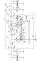
図1で示す車載用の電源システム100は、車載用の電源部として構成される第1電源部91及び第2電源部92と、車載用電源装置1(以下、電源装置1ともいう)とを備え、車両に搭載された負荷93,94に電力を供給し得るシステムとして構成されている。負荷93,94は、車載用電気部品であり、その種類や数は限定されない。
電源装置1の制御部30は、所定の開始条件の成立に応じて電圧変換部10を駆動し、電圧変換動作を行わせる。具体的には、例イグニッションスイッチがオン状態である場合に外部装置から制御部30に対してイグニッションオン信号が与えられるようになっており、イグニッションスイッチがオフ状態である場合に外部装置から制御部30に対してイグニッションオフ信号が与えられるようになっている。制御部30は、例えばイグニッションスイッチがオフ状態からオン状態に切り替わったことを開始条件として電圧変換部10に制御信号を与え、電圧変換部10に電圧変換動作を行わせる。具体的には、電圧検出部54によって監視される第2導電路22の電圧に基づき、第2導電路22の電圧を所望の目標電圧(基準導電路83の電圧よりも大きい所定電圧値であり、例えば第2電源部92の満充電時の出力電圧よりも少し大きい値)とするように、フィードバック演算を繰り返してPWM信号のデューティを調整しつつ電圧変換部10に降圧動作を行わせる。
制御部30は、上述した基本制御の実行中に、図5のような異常検出制御を繰り返し行う。異常検出制御を行う場合、まずステップS11において異常検出回路42,52,62のいずれかから異常検出信号が出力されているか否かを制御回路32が判定する。異常検出回路42,52,62のいずれからも異常検出信号が出力されていない場合(ステップS11にてNoの場合)には、図5の異常検出制御を終了した後、即座に図5の異常検出制御を開始するように繰り返す。異常検出回路42,52,62のいずれかから異常検出信号が出力されている場合(ステップS11にてYesの場合)には、制御回路32が駆動回路34に対して異常停止要求を与える(ステップS12)。ステップS12の後のステップS13では、異常停止要求を受けた駆動回路34が第1素子11、第2素子12、スイッチング素子15に与える信号S1,S2,S3をいずれもオフ信号とし、電圧変換部10の動作を停止させる。このように、異常検出回路42,52,62のいずれかで異常が検出され、異常検出信号が出力された場合には、第1素子11、第2素子12、スイッチング素子15をオフ動作させ、電圧変換部10を停止させることができる。
図2のように、故障検出装置3は、複数の異常検出回路42,52,62を備えた異常検出部36と、制御部30と、信号伝送部70とを含んだ構成をなす。故障検出装置3は、制御部30が主体となり、図6のような流れで故障検出制御を行う。
上述した故障検出装置3では、制御回路32の少なくとも一部が信号出力部32Aとして機能し、共通信号線71を介して検査用指示信号(複数の異常検出回路42,52,62に対して異常時の動作を指示する信号)を出力する。そして、信号分配部72は、制御回路32から共通信号線71に出力された検査用指示信号を複数の分岐信号線72A,72B,72Cによって各々の異常検出回路42,52,62に伝送する。このような構成であるため、実際には各異常検出回路42,52,62による検出対象位置に異常が生じていないときでも複数の異常検出回路42,52,62に異常時の動作を行わせることができる。更に制御回路32の少なくとも一部が判定部32Bとして機能し、検査用指示信号の出力時に複数の異常検出回路42,52,62から出力される信号に基づき、各々の異常検出回路42,52,62が故障であるか否かをそれぞれ判定することができる。しかも、複数の異常検出回路42,52,62に対して一斉に異常時の動作を指示することができ、これら異常検出回路42,52,62に検査用の動作を迅速に行わせることができるため、複数の異常検出回路42,52,62の少なくともいずれかにおいて故障が生じているか否かを、より短時間で判定することができる。
次に、実施例2について説明する。
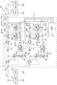
図7で示す車載用の電源システム200は、電源装置201のみが図1で示す車載用の電源システム100と異なる。実施例2の電源装置201は、第1導電路21と第2導電路22との間に電圧変換部10を複数並列に設けた点のみが実施例1の電源装置1と比較したときの回路構成上の相違点であり、それ以外の回路構成は実施例1と同様である。なお、図7では、制御部30から、各々の電圧変換部10のスイッチング素子(第1素子11、第2素子12、スイッチング素子15)に接続される信号線の図示は省略している。
本発明は上記記述及び図面によって説明した実施例に限定されるものではなく、例えば次のような実施例も本発明の技術的範囲に含まれる。また、上述した実施例や後述する実施例は矛盾しない範囲で組み合わせることが可能である。
この構成でも、制御部30における制御回路(図2、図3の制御回路32と同様の回路)の少なくとも一部が信号出力部32A(図2)と同様に機能し、実施例1と同様の検査用指示信号(複数の異常検出回路に対して異常時の動作を指示する信号)を、共通信号線71を介して出力する。信号分配部72は、信号出力部に相当する制御部30内の制御回路(図2、図3の制御回路32と同様の回路)から共通信号線71に出力される検査用指示信号を、各々の電圧変換部10に対応付けられた異常検出回路42,52,62にそれぞれ分配する構成となっている。そして、この構成でも、制御部30における制御回路(図2、図3の制御回路32と同様の回路)の少なくとも一部が判定部32B(図2)と同様に機能し、当該制御回路が共通信号線を介して検査用指示信号を出力したときに複数の異常検出回路(各々の電圧変換部10に対応する複数の異常検出回路42,52,62)から出力される信号に基づき、実施例1と同様の方法で各々の異常検出回路が故障であるか否かをそれぞれ判定する。
この構成によれば、部品点数が多くなりがちな多相式の電源装置において部品点数の削減やコストの低減を図りつつ、複数の異常検出部の少なくともいずれかにおいて故障が生じているか否かを、より短時間で判定し得る故障検出装置を実現することができる。
3…車載用電源装置の故障検出装置
10…電圧変換部
11…第1素子
12…第2素子
14…インダクタ
21…第1導電路
22…第2導電路
30…制御部
32…制御回路
32A…信号出力部
32B…判定部
36…異常検出部
42…異常検出回路(出力電流異常検出回路)
42B,52B,62B…比較部
44,54,64…電圧信号入力部
46,56,66…信号伝送路
52…異常検出回路(出力電圧異常検出回路)
62…異常検出回路(基準導電路側の異常検出回路)
71…共通信号線
72…信号分配部
72A,72B,72C…分岐信号線
83…基準導電路
Claims (6)
- 第1導電路と第2導電路とに接続されるとともに前記第1導電路及び前記第2導電路の一方の導電路に印加された電圧を昇圧又は降圧して他方の導電路に出力する動作を少なくとも行う電圧変換部と、前記電圧変換部を制御する制御部と、複数の検出対象位置で生じる電流又は電圧の異常を検出する複数の異常検出回路を備えるとともに各々の前記異常検出回路が電流又は電圧の異常を検出した場合に異常検出信号を出力する異常検出部と、を有する車載用電源装置の故障を検出する故障検出装置であって、
各々の前記異常検出回路に対して異常時の動作を指示する検査用指示信号を、共通信号線を介して出力する信号出力部と、
前記共通信号線から分岐する複数の分岐信号線を備え、前記信号出力部から前記共通信号線に出力された前記検査用指示信号を、各々の前記分岐信号線によって各々の前記異常検出回路に伝送する信号分配部と、
前記信号出力部が前記共通信号線を介して前記検査用指示信号を出力したときに各々の前記異常検出回路から出力される信号に基づき、各々の前記異常検出回路が故障であるか否かをそれぞれ判定する判定部と、
を有する車載用電源装置の故障検出装置。 - 前記異常検出部は、複数の前記異常検出回路として、前記電圧変換部の出力側の導電路の電流の異常を検出する出力電流異常検出回路と前記出力側の導電路の電圧の異常を検出する出力電圧異常検出回路とを備え、
前記信号分配部は、前記信号出力部から前記共通信号線に出力された前記検査用指示信号を、少なくとも前記出力電流異常検出回路と前記出力電圧異常検出回路とに分配する請求項1に記載の車載用電源装置の故障検出装置。 - 前記電圧変換部は、前記第1導電路に電気的に接続されたスイッチング素子からなる第1素子と、前記第1導電路と前記第1導電路の電位よりも低い所定の基準電位に保たれる基準導電路との間に電気的に接続されたスイッチング素子又はダイオードからなる第2素子と、前記第1素子及び前記第2素子と前記第2導電路との間に電気的に接続されたインダクタとを備え、
前記異常検出部は、前記異常検出回路として前記第2素子と前記基準導電路との間を流れる電流の異常を検出する基準導電路側の異常検出回路を備え、
前記信号分配部は、前記信号出力部から前記共通信号線に出力された前記検査用指示信号を、少なくとも前記基準導電路側の異常検出回路に分配する請求項1又は請求項2に記載の車載用電源装置の故障検出装置。 - 前記車載用電源装置は、前記電圧変換部が複数設けられ、
前記異常検出部は、各々の前記電圧変換部にそれぞれ対応付けて1又は複数の前記異常検出回路が設けられ、
前記信号分配部は、前記信号出力部から前記共通信号線に出力された前記検査用指示信号を、各々の前記電圧変換部に対応付けられた前記異常検出回路にそれぞれ分配する請求項1から請求項3のいずれか一項に記載の車載用電源装置の故障検出装置。 - 前記異常検出部は、
複数の前記検出対象位置にそれぞれ対応した複数の信号伝送路と、各々の前記検出対象位置での電圧又は電流に応じた電圧信号を各々の前記信号伝送路にそれぞれ印加する複数の電圧信号入力部と、
複数の前記電圧信号入力部にそれぞれ対応する複数の比較部と、
を備え、
前記比較部は、対応する前記電圧信号入力部によって対応する前記信号伝送路に印加された入力電圧を基準電圧と比較し、前記入力電圧と基準電圧とが所定の正常関係である場合に正常信号を出力し、前記入力電圧と基準電圧とが前記正常関係ではない異常関係である場合に異常信号を出力し、
前記信号分配部は、前記信号出力部から前記検査用指示信号が出力された場合に各々の前記比較部への入力経路である各々の前記信号伝送路に対し、基準電圧との関係が異常関係となる電圧を印加する請求項1から請求項4のいずれか一項に記載の車載用電源装置の故障検出装置。 - 前記電圧変換部と、前記制御部と、前記異常検出部と、請求項1から請求項5のいずれか一項に記載の故障検出装置とを含む車載用電源装置。
Priority Applications (4)
| Application Number | Priority Date | Filing Date | Title |
|---|---|---|---|
| JP2017001498A JP6729404B2 (ja) | 2017-01-09 | 2017-01-09 | 車載用電源装置の故障検出装置及び車載用電源装置 |
| PCT/JP2017/045688 WO2018128077A1 (ja) | 2017-01-09 | 2017-12-20 | 車載用電源装置の故障検出装置及び車載用電源装置 |
| US16/476,336 US20190353715A1 (en) | 2017-01-09 | 2017-12-20 | Failure detection device for onboard power supply device, and onboard power supply device |
| CN201780079604.1A CN110114966A (zh) | 2017-01-09 | 2017-12-20 | 车载用电源装置的故障检测装置及车载用电源装置 |
Applications Claiming Priority (1)
| Application Number | Priority Date | Filing Date | Title |
|---|---|---|---|
| JP2017001498A JP6729404B2 (ja) | 2017-01-09 | 2017-01-09 | 車載用電源装置の故障検出装置及び車載用電源装置 |
Publications (3)
| Publication Number | Publication Date |
|---|---|
| JP2018113740A JP2018113740A (ja) | 2018-07-19 |
| JP2018113740A5 JP2018113740A5 (ja) | 2019-06-13 |
| JP6729404B2 true JP6729404B2 (ja) | 2020-07-22 |
Family
ID=62791090
Family Applications (1)
| Application Number | Title | Priority Date | Filing Date |
|---|---|---|---|
| JP2017001498A Expired - Fee Related JP6729404B2 (ja) | 2017-01-09 | 2017-01-09 | 車載用電源装置の故障検出装置及び車載用電源装置 |
Country Status (4)
| Country | Link |
|---|---|
| US (1) | US20190353715A1 (ja) |
| JP (1) | JP6729404B2 (ja) |
| CN (1) | CN110114966A (ja) |
| WO (1) | WO2018128077A1 (ja) |
Families Citing this family (5)
| Publication number | Priority date | Publication date | Assignee | Title |
|---|---|---|---|---|
| JP6901509B2 (ja) * | 2019-01-08 | 2021-07-14 | Necプラットフォームズ株式会社 | インピーダンス低減装置、電源装置、電源、インピーダンス低減方法及びインピーダンス低減処理プログラム |
| US11422203B1 (en) * | 2019-02-15 | 2022-08-23 | Maxim Integrated Products, Inc. | Current sensing line fault detector |
| DE102019126953B3 (de) * | 2019-10-08 | 2020-10-08 | Eberspächer Controls Landau Gmbh & Co. Kg | Steuergerät für ein Fahrzeug |
| CN110879368B (zh) * | 2019-12-23 | 2022-07-08 | 卡斯柯信号(北京)有限公司 | Itcs车载电源数据的监测方法及装置 |
| JP2023077080A (ja) * | 2021-11-24 | 2023-06-05 | 株式会社デンソー | 異常検出装置 |
Family Cites Families (7)
| Publication number | Priority date | Publication date | Assignee | Title |
|---|---|---|---|---|
| JP3473779B2 (ja) * | 1994-07-14 | 2003-12-08 | 株式会社安川電機 | 電流検出器の故障検出方法 |
| JP4584118B2 (ja) * | 2005-11-11 | 2010-11-17 | 三菱電機株式会社 | 電源装置及びそれを用いたシーケンサシステム |
| JP2010057244A (ja) * | 2008-08-27 | 2010-03-11 | Yokogawa Electric Corp | 直流電源装置および制御方法 |
| JP2013110837A (ja) * | 2011-11-21 | 2013-06-06 | Denso Corp | 電源システム |
| CN104584423B (zh) * | 2013-08-12 | 2017-06-13 | 日本精工株式会社 | 马达控制装置、使用该马达控制装置的电动助力转向装置以及车辆 |
| JP6506644B2 (ja) * | 2015-07-09 | 2019-04-24 | 日立オートモティブシステムズ株式会社 | 駆動装置 |
| JP6766506B2 (ja) * | 2016-08-02 | 2020-10-14 | 株式会社オートネットワーク技術研究所 | 異常検出装置及び車載用電源装置 |
-
2017
- 2017-01-09 JP JP2017001498A patent/JP6729404B2/ja not_active Expired - Fee Related
- 2017-12-20 US US16/476,336 patent/US20190353715A1/en not_active Abandoned
- 2017-12-20 WO PCT/JP2017/045688 patent/WO2018128077A1/ja active Application Filing
- 2017-12-20 CN CN201780079604.1A patent/CN110114966A/zh active Pending
Also Published As
| Publication number | Publication date |
|---|---|
| CN110114966A (zh) | 2019-08-09 |
| US20190353715A1 (en) | 2019-11-21 |
| WO2018128077A1 (ja) | 2018-07-12 |
| JP2018113740A (ja) | 2018-07-19 |
Similar Documents
| Publication | Publication Date | Title |
|---|---|---|
| JP6729404B2 (ja) | 車載用電源装置の故障検出装置及び車載用電源装置 | |
| JP6358304B2 (ja) | 車両用電源装置 | |
| JP6281553B2 (ja) | Dcdcコンバータ | |
| US10601301B2 (en) | Abnormality detection device and vehicle-mounted power supply device | |
| US9640980B2 (en) | Power interrupting device | |
| CN108141132B (zh) | 多相转换器 | |
| JP6414533B2 (ja) | 多相コンバータ | |
| KR102088893B1 (ko) | 양방향 dc-dc 컨버터의 보호 장치 및 방법 | |
| WO2019181422A1 (ja) | 車載用の多相コンバータ | |
| JP6497565B2 (ja) | Dcdcコンバータ | |
| JP2017212805A (ja) | 車両用電圧変換装置 | |
| KR102123375B1 (ko) | 양방향 dc-dc 컨버터의 보호 장치 및 방법 | |
| JP6748921B2 (ja) | 車載用電源回路及び車載用電源装置 | |
| JP6677905B2 (ja) | 異常検出装置及び電源装置 | |
| KR20190111000A (ko) | 양방향 dc-dc 컨버터의 보호 장치 및 방법 | |
| JP2019186880A (ja) | 負荷駆動装置 | |
| US11476750B2 (en) | Vehicle power supply device with charge circuit section | |
| JP2018078738A (ja) | 車載用の降圧型dcdcコンバータ | |
| JP2018129951A (ja) | 車載用電源装置の異常検出装置及び車載用電源装置 | |
| KR102123374B1 (ko) | 양방향 dc-dc 컨버터의 보호 장치 및 방법 | |
| KR102088889B1 (ko) | 양방향 dc-dc 컨버터의 보호 장치 및 방법 | |
| KR102033548B1 (ko) | 양방향 dc-dc 컨버터의 보호 장치 및 방법 | |
| KR20190110998A (ko) | 양방향 dc-dc 컨버터의 보호 장치 및 방법 | |
| KR20190110999A (ko) | 양방향 dc-dc 컨버터의 보호 장치 및 방법 | |
| JP2007228654A (ja) | スイッチング電源 |
Legal Events
| Date | Code | Title | Description |
|---|---|---|---|
| A621 | Written request for application examination |
Free format text: JAPANESE INTERMEDIATE CODE: A621 Effective date: 20190424 |
|
| A521 | Request for written amendment filed |
Free format text: JAPANESE INTERMEDIATE CODE: A523 Effective date: 20190508 |
|
| TRDD | Decision of grant or rejection written | ||
| A01 | Written decision to grant a patent or to grant a registration (utility model) |
Free format text: JAPANESE INTERMEDIATE CODE: A01 Effective date: 20200602 |
|
| A61 | First payment of annual fees (during grant procedure) |
Free format text: JAPANESE INTERMEDIATE CODE: A61 Effective date: 20200615 |
|
| R150 | Certificate of patent or registration of utility model |
Ref document number: 6729404 Country of ref document: JP Free format text: JAPANESE INTERMEDIATE CODE: R150 |
|
| LAPS | Cancellation because of no payment of annual fees |