JP6727847B2 - Radiation imaging apparatus, radiation imaging system, and method of controlling radiation imaging apparatus - Google Patents
Radiation imaging apparatus, radiation imaging system, and method of controlling radiation imaging apparatus Download PDFInfo
- Publication number
- JP6727847B2 JP6727847B2 JP2016035845A JP2016035845A JP6727847B2 JP 6727847 B2 JP6727847 B2 JP 6727847B2 JP 2016035845 A JP2016035845 A JP 2016035845A JP 2016035845 A JP2016035845 A JP 2016035845A JP 6727847 B2 JP6727847 B2 JP 6727847B2
- Authority
- JP
- Japan
- Prior art keywords
- voltage
- radiation imaging
- radiation
- drive
- imaging apparatus
- Prior art date
- Legal status (The legal status is an assumption and is not a legal conclusion. Google has not performed a legal analysis and makes no representation as to the accuracy of the status listed.)
- Active
Links
- 230000005855 radiation Effects 0.000 title claims description 187
- 238000003384 imaging method Methods 0.000 title claims description 96
- 238000000034 method Methods 0.000 title claims description 20
- 239000010409 thin film Substances 0.000 claims description 73
- 239000004065 semiconductor Substances 0.000 claims description 43
- 238000006243 chemical reaction Methods 0.000 claims description 19
- 239000003990 capacitor Substances 0.000 claims description 18
- 238000012545 processing Methods 0.000 claims description 15
- 238000009825 accumulation Methods 0.000 claims description 10
- 239000011159 matrix material Substances 0.000 claims description 5
- 206010041347 Somnambulism Diseases 0.000 description 12
- 230000003321 amplification Effects 0.000 description 11
- 238000003199 nucleic acid amplification method Methods 0.000 description 11
- 230000010365 information processing Effects 0.000 description 10
- 230000001629 suppression Effects 0.000 description 7
- 229910021417 amorphous silicon Inorganic materials 0.000 description 3
- 230000005684 electric field Effects 0.000 description 3
- MCVAAHQLXUXWLC-UHFFFAOYSA-N [O-2].[O-2].[S-2].[Gd+3].[Gd+3] Chemical group [O-2].[O-2].[S-2].[Gd+3].[Gd+3] MCVAAHQLXUXWLC-UHFFFAOYSA-N 0.000 description 2
- 230000015572 biosynthetic process Effects 0.000 description 2
- XQPRBTXUXXVTKB-UHFFFAOYSA-M caesium iodide Chemical compound [I-].[Cs+] XQPRBTXUXXVTKB-UHFFFAOYSA-M 0.000 description 2
- 238000005229 chemical vapour deposition Methods 0.000 description 2
- 238000012937 correction Methods 0.000 description 2
- 238000010586 diagram Methods 0.000 description 2
- 239000010408 film Substances 0.000 description 2
- 230000001678 irradiating effect Effects 0.000 description 2
- 239000000463 material Substances 0.000 description 2
- 239000000758 substrate Substances 0.000 description 2
- 238000012935 Averaging Methods 0.000 description 1
- BUGBHKTXTAQXES-UHFFFAOYSA-N Selenium Chemical compound [Se] BUGBHKTXTAQXES-UHFFFAOYSA-N 0.000 description 1
- 230000002411 adverse Effects 0.000 description 1
- 239000012212 insulator Substances 0.000 description 1
- 230000010354 integration Effects 0.000 description 1
- 229910021420 polycrystalline silicon Inorganic materials 0.000 description 1
- 229920005591 polysilicon Polymers 0.000 description 1
- 229910052711 selenium Inorganic materials 0.000 description 1
- 239000011669 selenium Substances 0.000 description 1
Images


Description
本発明は、放射線撮像装置、放射線撮像システム及び放射線撮像装置の制御方法に関する。 The present invention relates to a radiation image pickup apparatus, a radiation image pickup system, and a control method of the radiation image pickup apparatus.
放射線撮像装置は、放射線が照射された画像(以下、放射線照射画像という)と放射線が照射されない画像(以下、ダーク画像という)の差分によって画像を生成する。特に、放射線撮像装置内に配置され、光の情報を電子の情報に変換する光電変換素子がアモルファスシリコンで作られている場合、ダーク画像の情報を考慮しなければ、正確な画像を生成することは困難である。このダーク画像は、放射線撮像装置内の温度に強く依存し、温度が上昇するとダーク成分が増加する性質がある。また、放射線によって得られた電荷を積算するための増幅回路の特性も温度に依存し、通常、増幅回路に電力が供給されるとしばらくは温度ドリフトのために特性が安定しない。 The radiation imaging apparatus generates an image by a difference between an image irradiated with radiation (hereinafter referred to as a radiation irradiation image) and an image not irradiated with radiation (hereinafter referred to as a dark image). In particular, if the photoelectric conversion element that is arranged in the radiation imaging device and that converts light information into electronic information is made of amorphous silicon, it is necessary to generate an accurate image unless dark image information is taken into consideration. It is difficult. This dark image has a property that it strongly depends on the temperature in the radiation imaging apparatus, and the dark component increases as the temperature rises. Further, the characteristics of the amplifier circuit for integrating the charges obtained by the radiation also depend on the temperature, and normally, when power is supplied to the amplifier circuit, the characteristics are not stable due to temperature drift for a while.
そのため、アモルファスシリコンを用いた放射線撮像装置の場合、電源投入後、放射線撮像装置内の温度や増幅回路の温度が一定になり、ダーク成分や温度ドリフトを一定にするために暖気運転が行われる場合がある。しかし、救急病院など緊急に放射線撮像装置が必要になる場合、このようなダーク成分や温度ドリフトが一定になる時間が必要なのは非常に都合勝手が悪い。ダーク画像や温度ドリフトが一定にならないことにより、放射線照射画像とダーク画像の差分で構成される画像は信頼性のある画像とは言えないからである。 Therefore, in the case of a radiation imaging device using amorphous silicon, after power is turned on, the temperature inside the radiation imaging device and the temperature of the amplification circuit become constant, and warm-up operation is performed to make the dark component and temperature drift constant. There is. However, when a radiation imaging apparatus is urgently needed such as in an emergency hospital, it is very inconvenient to require such a time that the dark component and the temperature drift become constant. Because the dark image and the temperature drift are not constant, the image formed by the difference between the radiation irradiation image and the dark image cannot be said to be a reliable image.
そのため、下記の特許文献1に示すように、近年、放射線撮像装置はいつでも瞬時に使用できるように常に電源をオン状態にして暖気運転をすることが行われている。特許文献1では、放射線撮像装置内の光電変換素子や光電変換素子に蓄積された電荷を読み出すための薄膜トランジスタに印加する電圧を、すべてグランドに落とす。特許文献1では、それをスリープ状態と定義している。しかしながら、それでは、緊急時に、ダーク成分が一定の状態で、放射線撮像装置を使用することは困難である。なぜならば、通常、放射線撮像装置は、光電変換素子に電荷を蓄積するために、ある一定の電圧を印加して使用する。そのため、スリープ状態では、上記の電圧をグランドに落としておいて、緊急時に使用する瞬間に光電変換素子に急に電圧を印加すると、光電変換素子内の電荷が定常状態に達するまでにある程度の時間を要するという課題が生じる。その間、ダーク成分は安定せず、信頼性のある画像データを取得することが困難である。
Therefore, as shown in
また、一般の放射線撮像装置において、増幅回路を駆動させつつ、通常の読み出し駆動と同じタイミングを使用しながら、光電変換素子と薄膜トランジスタに印加する電圧を暖気運転により駆動する方法がとられている。しかしながら、その方法では、薄膜トランジスタの閾値電圧が変化し、特性の変化を引き起こすという課題が生じる。暖気運転期間の割合は、非常に長くなることがあり、その分だけ閾値の変化は激しくなる。閾値の変化が生じると、トランジスタからリークする成分が変化し、結果として画像に対しても悪い影響を与える。 Further, in a general radiation imaging apparatus, a method is used in which the voltage applied to the photoelectric conversion element and the thin film transistor is driven by a warming-up operation while driving the amplifier circuit and using the same timing as the normal read driving. However, this method has a problem that the threshold voltage of the thin film transistor changes, causing a change in characteristics. The ratio of the warm-up period may become very long, and the threshold value may change significantly accordingly. When the threshold value changes, the component leaking from the transistor changes, and as a result, it adversely affects the image.
特許文献1で開示されているようなスリープ状態の駆動方法では、増幅回路の温度ドリフトを軽減することはできても、緊急時の使用においてセンサ基板特有のダーク成分の変化を防ぎつつ、かつ、薄膜トランジスタの閾値を一定に保つことは困難である。
In the sleep state driving method as disclosed in
本発明の目的は、緊急時の使用においてダーク成分の変化を防ぎ、トランジスタの閾値電圧の変化を防ぎ、緊急時にも常に安定した画像を生成することができる放射線撮像装置、放射線撮像システム及び放射線撮像装置の制御方法を提供することである。 An object of the present invention is to prevent a dark component from changing during use in an emergency, prevent a change in a threshold voltage of a transistor, and always generate a stable image even in an emergency, a radiation imaging system, a radiation imaging system, and a radiation imaging system. A method of controlling a device is provided.
本発明の放射線撮像装置は、各々が変換素子とトランジスタとを含み、行列状の配列された、放射線に応じた電気信号を生成する複数の画素と、前記複数の画素の前記トランジスタのゲートに電気的に接続された複数の駆動線と、前記複数の画素を駆動するために前記複数の駆動線に電圧を供給する駆動回路部と、前記駆動回路部を制御する制御部とを有し、前記変換素子が、放射線を光に変換するシンチレータ及び前記光を電荷に変換するフォトダイオードを含み、前記フォトダイオードが、第1電極と第2電極の間に配置された真性半導体層と、前記第1電極と前記真性半導体層との間に配置された第1型半導体層と、前記真性半導体層と前記第2電極の間に配置された第2型半導体層と、を含み、前記トランジスタが、第1導電型の半導体層を有し、そのソース及びドレインのうちの一方が前記第1電極に電気的に接続された第1型薄膜トランジスタであり、前記制御部が、前記駆動回路部に前記トランジスタをオフさせるためのオフ電圧を前記複数の駆動線に供給させることにより前記複数の画素に前記電気信号を蓄積させる蓄積制御と、前記駆動回路部に前記トランジスタをオンさせるためのオン電圧を前記複数の駆動線に順に供給させることにより前記複数の画素から前記電気信号を読み出す本読み制御と、前記蓄積制御を行う期間及び前記本読み制御を行う期間とは別の期間に、前記駆動回路部に前記オフ電圧と前記オン電圧との間であって前記オフ電圧及び前記オン電圧とは異なる電圧と前記オン電圧とを交互に前記複数の駆動線に供給させる制御を行うことを特徴とする。 The radiation imaging apparatus of the present invention includes a plurality of pixels, each including a conversion element and a transistor, arranged in a matrix to generate an electric signal according to radiation, and a plurality of pixels each having a gate electrically connected to the transistor. Electrically connected to each other, a drive circuit unit that supplies a voltage to the plurality of drive lines to drive the plurality of pixels, and a control unit that controls the drive circuit unit, The conversion element includes a scintillator that converts radiation into light and a photodiode that converts the light into charges, the photodiode including an intrinsic semiconductor layer disposed between a first electrode and a second electrode, and the first semiconductor layer. A first type semiconductor layer disposed between an electrode and the intrinsic semiconductor layer, and a second type semiconductor layer disposed between the intrinsic semiconductor layer and the second electrode; A first-type thin film transistor having a one-conductivity-type semiconductor layer, one of a source and a drain of which is electrically connected to the first electrode, and the control unit includes the transistor in the drive circuit unit. An accumulation control for accumulating the electric signal in the plurality of pixels by supplying an off-voltage for turning off to the plurality of drive lines, and an on-voltage for causing the drive circuit unit to turn on the transistor. a real reading control for reading the electric signal from said plurality of pixels by sequentially supplied to the drive line, to a different time period and the period and the period of performing the real reading control for the storage control, the off-voltage to the drive circuit unit Between the ON voltage and the ON voltage and a voltage different from the OFF voltage and the ON voltage and the ON voltage are alternately supplied to the plurality of drive lines.
本発明によれば、緊急時の使用においてダーク成分の変化を防ぎ、トランジスタの閾値電圧の変化を防ぎ、緊急時にも常に安定した画像を生成することができる。 According to the present invention, it is possible to prevent a dark component from changing during use in an emergency, prevent a threshold voltage of a transistor from changing, and always generate a stable image even in an emergency.
(第1の実施形態)
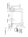
図1は、本発明の第1の実施形態による放射線撮像システム100の構成例を示す図である。放射線撮像システム100は、曝射スイッチ101、放射線源制御部102、放射線源103、放射線撮像装置105、情報処理部106、及び被写体情報入力装置/画像表示装置107を有する。放射線撮像装置105は、放射線撮像装置105の電源スイッチ105aを有する。曝射スイッチ101は、放射線源制御部102に対して有線ケーブルで電気的に接続され、スイッチ信号を放射線源制御部102に出力する。放射線源制御部102は、スイッチ信号に応じて放射線源103を制御する。放射線源103は、放射線源制御部102の制御の下、放射線104を照射する。放射線104は、患者を介して、放射線撮像装置105に照射される。医師や技師は、曝射スイッチ101の操作により、放射線104を患者に向けて照射することができる。放射線源制御部102は、曝射スイッチ101、放射線源103及び情報処理部106に電気的に接続される。情報処理部106は、被写体情報入力装置/画像表示装置107、及び放射線撮像装置105に電気的に接続される。放射線撮像装置105は、入射した放射線を電気信号に変換し、その電気信号を情報処理部106に出力する。情報処理部106は、入力した信号を処理し、その処理結果を放射線源制御部102に出力する。また、放射線撮像装置105は、入射した放射線を電気信号の画像に変換し、その画像を情報処理部106に出力する。情報処理部106は、入力した画像を処理し、その処理した画像を被写体情報入力/画像表示装置107に出力する。被写体情報入力/画像表示装置107は、その画像を表示する。
(First embodiment)
FIG. 1 is a diagram showing a configuration example of a radiation imaging system 100 according to the first embodiment of the present invention. The radiation imaging system 100 includes an
電源スイッチ105aを操作することにより、放射線撮像装置105の電源がオン状態になり、放射線撮像装置105が使用可能になる。この電源スイッチ105aを操作することにより、放射線撮像装置105内において、センサ基板に電圧が印加され、増幅回路は駆動を始める。また、曝射スイッチ101、放射線源制御部102、放射線源103、放射線撮像装置105、情報処理部106、及び被写体情報入力装置/画像表示装置107は、それぞれ入出力端子を有し、互いに信号の通信をすることができる。
By operating the power switch 105a, the radiation imaging apparatus 105 is turned on, and the radiation imaging apparatus 105 becomes usable. By operating the power switch 105a, a voltage is applied to the sensor substrate in the radiation imaging apparatus 105, and the amplifier circuit starts driving. Further, the
図2は、図1の放射線撮像装置105の構成例を示す図である。放射線撮像装置105は、回路部105b及び画素アレイ部201を有する。画素アレイ部201は、行列状に配列された複数の画素200を有する。複数の画素200の各々は、フォトダイオード202及び薄膜トランジスタ203を有する。薄膜トランジスタ203は、ゲート電極203a、ソース電極203b及びドレイン電極203cを有する。画素200内において、フォトダイオード202のカソード(変換素子の第2の端子)は、薄膜トランジスタ203のドレイン電極203cに電気的に接続される。複数の駆動線205は、それぞれ、各行の画素200内の薄膜トランジスタ203のゲート電極203aに共通に電気的に接続される。複数の信号線204は、それぞれ、各列の画素200内の薄膜トランジスタ203のソース電極203bに共通に電気的に接続される。複数の共通電圧線224は、それぞれ、各列の画素200内のフォトダイオード202のアノード(変換素子の第1の端子)に共通に電気的に接続される。なお、薄膜トランジスタ203のソース電極203b及びドレイン電極203cのうちの一方はフォトダイオード202のカソード(変換素子の第2の端子)に電気的に接続され、他方は複数の信号線204のうちのいずれかに電気的に接続されればよい。
FIG. 2 is a diagram showing a configuration example of the radiation imaging apparatus 105 of FIG. The radiation imaging apparatus 105 has a
回路部105bは、駆動回路部206、制御部210、メモリ211、共通電圧印加回路部213及び信号処理部217を有する。信号処理部217は、各列の増幅回路207、サンプルホールド回路214、マルチプレクサ208及びアナログデジタル変換器(ADC)209を有し、複数の信号線204に電気的に接続される。複数の増幅回路207は、それぞれ、複数の信号線204に電気的に接続される。複数の増幅回路207の各々は、差動増幅器207a、容量207b及びリセットスイッチ207cを有する。差動増幅器207aは、反転入力端子に複数の信号線204のうちの対応する1つの信号線204の電圧を入力し、非反転入力端子に基準電圧Vrefを入力する。容量207b及びリセットスイッチ207cは、差動増幅器207aの反転入力端子及び出力端子間に電気的に接続される。駆動回路部206は、複数の駆動線205の電圧を制御する駆動線制御部である。共通電圧印加回路部213は、複数の共通電圧線224に同じ電圧を印加する共通電圧印加部である。すなわち、共通電圧印加回路部213は、すべての画素200内のフォトダイオード202のアノードに同じ電圧を印加する。
The
図3(a)、(b)は、図2のフォトダイオード202及び薄膜トランジスタ203の構成例を示す断面図である。図3(a)はフォトダイオード202がPIN型フォトダイオードである例を示す。PIN型フォトダイオード202は、上からP型半導体層301、真性半導体層302、及びN型半導体層303を有する。P型半導体層301の上部には共通電極202bが設けられ、N型半導体層303の下部には個別電極202aが設けられる。また、図2の薄膜トランジスタ203は、ゲート電極203a、ソース電極203b、ドレイン電極203c、N型半導体層304及び真性半導体層305を有する。ドレイン電極203cは、PIN型フォトダイオード202の個別電極202aに電気的に接続される。図3(b)は図2のフォトダイオード202及び薄膜トランジスタ203の他の構成例を示す断面図である。フォトダイオード202がMIS型フォトダイオードである例を示す。MIS型フォトダイオード202は、上からN型半導体層401、真性半導体層402、及び絶縁層403を有する。N型半導体層401の上部には共通電極202bが設けられ、絶縁層403の下部には個別電極202aが設けられる。また、図2の薄膜トランジスタ203は、ゲート電極203a、ソース電極203b、ドレイン電極203c、N型半導体層404及び真性半導体層405を有する。ドレイン電極203cは、MIS型フォトダイオード202の個別電極202aに電気的に接続される。
3A and 3B are cross-sectional views showing configuration examples of the
次に、図2〜図3を用いて、放射線撮像装置105の説明を行う。放射線撮像装置105は、画素アレイ部201及び回路部105bを有する。放射線撮像装置105は、放射線104を直接電気信号に変換して信号電荷を得る直接型と、放射線を可視光に変換してから可視光を信号電荷に変換する間接型が存在する。間接型の場合、画素アレイ部201にシンチレータが設けられる。シンチレータは、放射線撮像装置105の画素アレイ部201の全面を覆うように配置される。シンチレータの材料は、ガドリニウムオキシサルファイド(GOS)やヨウ化セシウム(CsI)などである。シンチレータは、放射線を可視光に変換する。フォトダイオード202は、その可視光を電気信号(電荷)に変換する。シンチレータ及びフォトダイオード202は、放射線に応じた電気信号を生成する変換素子である。直接型の場合、シンチレータは不要であり、フォトダイオード202の代わりに、放射線を電気信号に直接変換する変換素子が設けられる。
Next, the radiation imaging apparatus 105 will be described with reference to FIGS. The radiation imaging apparatus 105 has a
画素アレイ部201は、駆動回路部206及び共通電圧印加回路部213により制御される。画素アレイ部201は、m個(x方向)×n個(y方向)の行列状の複数の画素200を有する。画素200は、フォトダイオード202及び薄膜トランジスタ203を有する。薄膜トランジスタ203は、駆動線205の電圧に応じて、フォトダイオード202により変換された電荷を信号線204に出力する。画素200は、x方向及びy方向にそれぞれ1000画素〜4000画素程度存在し、総画素数は1千万程度である。駆動線205はx方向に、信号線204はy方向に、それぞれ延びており、互いに直交している。1本の駆動線205には、同一行のすべての画素200のゲート電極203aが電気的に接続されている。また、1本の信号線204には、同一列のすべての画素200のソース電極203bが電気的に接続されている。
The
フォトダイオード202は、例えば、図3(a)に示すように、上からP型半導体層301、真性半導体層302及びN型半導体層303を有するPIN型フォトダイオードである。また、それと逆の構造で、上からN型半導体層、真性半導体層、P型半導体層を有するNIP型フォトダイオード202を用いてもよい。また、図3(b)に示すように、上からN型半導体層401、真性半導体層402及び絶縁体層403を有するMIS型フォトダイオード202を用いてもよい。このMIS型フォトダイオード202は、半導体層がP型半導体でもよい。フォトダイオード202は、個別電極202aと共通電極202bの2つの電極を有しており、どちらかの電極が共通電圧印加回路部213により電位が固定されている。図3(a)では、個別電極202aがフォトダイオード202の下部に配置され、薄膜トランジスタ203に電気的に接続されている。共通電極202bが共通電圧印加回路部213により電位が固定される。その結果、フォトダイオード202内には電場が生じる。共通電極202bの電位が固定された状態で、放射線が入射された際、フォトダイオード202内で電子とホールのペアが生じる。この電子とホールの一方は共通電圧印加回路部213により生じた電場により引き寄せられ、固定されていない個別電極202aに電荷が蓄積され、電位が変動する。例えば、N型薄膜トランジスタ203とMIS型フォトダイオード202の場合、薄膜トランジスタ203と個別電極202bが電気的に接続されており、個別電極202bの電位が放射線入射により変動する。フォトダイオード202の材料は、直接型の場合、アモルファスセレンなどが良い。間接型の場合は、フォトダイオード202の半導体はアモルファスシリコンでもよいし、ポリシリコンでもよい。
The
薄膜トランジスタ203は、スイッチング素子であり、ゲート電極203a、ソース電極203b、及びドレイン電極203cを有する。薄膜トランジスタ203は、N型半導体層が使用されるN型薄膜トランジスタでもよいし、P型半導体層が使用されるP型薄膜トランジスタでもよい。N型薄膜トランジスタ203の場合、ゲート電極203aの電圧が閾値電圧より高い電圧Vonになると、薄膜トランジスタ203のスイッチ特性はオン状態となる。P型薄膜トランジスタ203の場合は、その逆で、ゲート電極203aの電圧が閾値電圧より低い電圧Vonになると、薄膜トランジスタ203のスイッチ特性はオン状態となる。ゲート電極203aは駆動線205に電気的に接続され、ソース電極203bは信号線204に電気的に接続され、ドレイン電極203cはフォトダイオード202の個別電極202aに電気的に接続されている。また、薄膜トランジスタ203の構造は、駆動線205が薄膜トランジスタ203の下部に位置するようなボトムゲート型の薄膜トランジスタでもよいし、上部に位置するトップゲート型の薄膜トランジスタでもよい。
The
フォトダイオード202と薄膜トランジスタ203は、CVD(Chemical Vapor Deposition:化学気相成長)装置を用いて形成される。センサ部202と薄膜トランジスタ203は、同一の成膜時に形成してもよいし、別々の成膜で形成してもよい。例えば、図3(a)と図3(b)のように、フォトダイオード202を薄膜トランジスタ203の上部に形成するような積層型でもよい。
The
駆動回路部206は、各行の駆動線205に電気的に接続され、行単位で、薄膜トランジスタ203のゲート電極203aの電圧を制御する。1本の駆動線205には同一行のすべての画素200のゲート電極203aが電気的に接続されているため、駆動回路部206は、行単位で、薄膜トランジスタ203を制御することができる。駆動線205に薄膜トランジスタ203のスイッチ特性が閾値電圧Vthを超えて十分オンになるような電圧Vonが印加されると、画素200に蓄積された電気信号が信号線204及び増幅回路207へ転送される。駆動回路部206は、第1行から第n行まで行単位で順に駆動線205に電圧Vonを印加し、すべての行の画素200の電気信号を読み出すように、画素アレイ部201の駆動を行う。
The
薄膜トランジスタ203がN型薄膜トランジスタの場合、駆動回路部206は、薄膜トランジスタ203のオフ状態では−15〜−5ボルト程度のマイナスの電圧Voffをゲート電極203aに印加する。また、駆動回路部206は、薄膜トランジスタ203のオン状態では、5〜20ボルト程度の高い電圧Vonをゲート電極203aに印加する。
When the
これに対し、薄膜トランジスタ203がP型薄膜トランジスタの場合、駆動回路部206は、薄膜トランジスタ203のオフ状態では5〜20ボルト程度の高い電圧Voffをゲート電極203aに印加する。また、駆動回路部206は、薄膜トランジスタ203のオン状態では、−15〜−5ボルト程度の電圧Vonをゲート電極203aに印加する。
On the other hand, when the
薄膜トランジスタ203のゲート電極203aには、オフ状態の電圧Voffがほとんどの割合で印加される。その結果、N型薄膜トランジスタ203では、マイナスの電圧がゲート電極203aに支配的に印加され、閾値電圧はマイナス方向へシフトする。P型薄膜トランジスタ203の場合は、プラスの電圧がゲート電極203aに支配的に印加され、閾値電圧はプラス方向へシフトする。
The off-state voltage Voff is applied to the
制御部210は、増幅回路207内のリセットスイッチ207c、マルチプレクサ208、ADC209、メモリ211、駆動回路部206、共通電圧印加回路部213及びサンプルホールド回路214の制御を行う。各列の増幅回路207は、信号線204とサンプルホールド回路214と制御部210に電気的に接続され、それぞれ、各列の信号線204の電荷を電圧に変換し、その電圧をサンプルホールド回路214に出力する。放射線の入射後、駆動回路部206が1本の駆動線205に電圧Vonを印加すると、一行分の画素200の電荷が各列の信号線204に出力される。各列の増幅回路207は、各列の信号線204の電荷を電圧に変換し、その電圧をサンプルホールド回路214に出力する。駆動回路部206は、すべての行の駆動線205に電圧を印加した後、再び第1行から電圧を印加し始めるが、その時、増幅回路207に入力される電荷はそれまでの入力電荷との積分の値となる。制御部210が、増幅回路リセット線212を介して、リセットスイッチ207cをオン状態にすることにより、増幅回路207の入力電荷がリセットされる。その後、リセットスイッチ207cをオフ状態にすれば、増幅回路207のリセット状態が解除される。リセットスイッチ207cは、1画素分の信号の処理毎に入力電荷をリセットする。
The
サンプルホールド回路214は、サンプルホールドスイッチ215及びサンプルホールド容量216を有する。制御部210がサンプルホールドスイッチ215をオンにすると、増幅回路207の出力信号がサンプルホールド容量216に書き込まれる。サンプルホールドスイッチ215がオフになると、サンプルホールド容量216の信号は、保持され、マルチプレクサ208に出力される。
The
マルチプレクサ208は、ADC209及びサンプルホールド回路214に電気的に接続され、各列のサンプルホールド回路214の出力電圧を、順次、ADC209へ出力する。ADC209は、制御部210及びメモリ211に電気的に接続され、入力されたアナログ電圧をデジタル信号に変換し、そのデジタル信号をメモリ211に出力する。メモリ211は、入力したデジタル信号を、そのデジタル信号に対応する画素200の位置情報(x方向の座標情報とy方向の座標情報)と共に順次保存する。
The
共通電圧印加回路部213は、共通電圧線224を介して、図3(a)及び図3(b)に示すように、フォトダイオード202の共通電極202bに電気的に接続され、フォトダイオード202へ印加する電圧を制御する。放射線が入力すると、フォトダイオード202は、電子とホールが生成するが、フォトダイオード202にある一定の電界がかかっていないと、すぐに電子とホールが再結合し、画素200の信号が読み出せない。また、検出できる放射線の最大の量は、共通電圧印加回路部213がフォトダイオード202へ印加する電圧に依存する。共通電圧印加回路部213がフォトダイオード202の共通電極202bに印加する電圧をVs、増幅回路207の基準電圧をVref、フォトダイオード202の容量をCと置くと、フォトダイオード202に蓄積される電荷量は、C×|Vs−Vref|となる。VsとVrefの差分が大きいほど、フォトダイオード202は、多くの電荷量を蓄積することが可能である。
The common voltage
図4は、本実施形態による放射線撮像システム100の駆動方法(制御方法)を示すタイミングチャートであり、放射線撮像システム100が静止画を撮影する場合の駆動方法を示す。図4では、電源電圧503、放射線信号502及び駆動信号501を示す。電源電圧503は、放射線撮像装置105の電源電圧であり、電源スイッチ105aを操作することにより、電源電圧503が印加される。放射線信号502は、放射線源制御部102から放射線源103に供給される信号である。放射線信号502のローレベル期間では、放射線源103は放射線104を照射せず、放射線信号502のハイレベル期間では、放射線源103は放射線104を照射する。なお、増幅回路207を駆動させつつ、駆動回路部206による画素アレイ部201の駆動を行わない放射線撮像装置105の駆動を、スリープ駆動と定義する。また、増幅回路207を駆動させつつ、駆動回路部206による画素アレイ部201の駆動を行う放射線撮像装置105の駆動を、アイドリング駆動と定義する。
FIG. 4 is a timing chart showing the driving method (control method) of the radiation imaging system 100 according to the present embodiment, and shows the driving method when the radiation imaging system 100 captures a still image. In FIG. 4, the
駆動信号501は、制御部210から駆動回路部206及び信号処理部217に供給される信号である。駆動信号501は、空読み駆動信号501a、本読み駆動信号501b及びスリープ駆動信号501cを含む。空読み駆動信号501aのハイレベルパルスは、図5(a)の処理を示す。本読み駆動信号501bのハイレベルパルスは、図5(b)の処理を示す。スリープ駆動信号501cは、図6(a)もしくは図6(b)の処理を示す。図5及び図6では、第1行の画素200のゲート電極203aの電圧Vg1、第2行の画素200のゲート電極203aの電圧Vg2、第3行の画素200のゲート電極203aの電圧Vg3、及び第m行の画素200のゲート電極203aの電圧Vgmを示す。さらに、図5及び図6では、共通電極202bの電圧、増幅回路207の基準電圧Vref、及びサンプルホールド回路214の動作を示す。
The
まず、図4において、電源電圧503が印加されると、放射線信号502はローレベルであり、放射線撮像装置105は、スリープ駆動シーケンス504aの駆動を行う。スリープ駆動シーケンス504aでは、スリープ駆動信号501c又は501dがハイレベルになり、図6(a)もしくは図6(b)の処理を行う。スリープ駆動シーケンス504aでは、図6(a)もしくは図6(b)に示すように、駆動回路部206は、すべての行の画素200のゲート電極203aの電圧Vg1〜VgmをVoff1にする。電圧Voff1は、図5(a)に示すオン電圧Vonより低くかつオフ電圧Voffより高い電圧であり、薄膜トランジスタ203をオフにする電圧である必要はない。すなわち、駆動回路部206は、オフ電圧Voffとオン電圧Vonとの間の電圧であって、オフ電圧Voff及びオン電圧Vonとは異なる電圧Voff1を複数の駆動線205に供給する。具体的には、制御部210は、駆動回路部206にオフ電圧Voffと薄膜トランジスタ203の閾値電圧Vthとの間であってオフ電圧Voff及び閾値電圧Vthとは異なる電圧Voff1を複数の駆動線205に供給させる。電圧Voff1は、例えば0〜5Vである。好ましくは、電圧Voff1は、薄膜トランジスタ203の閾値電圧をVthとすると、閾値電圧Vthより低くかつオフ電圧Voffより高い電圧である。また、薄膜トランジスタ203の閾値電圧をVthとすると、電圧Voff1は、増幅回路207の基準電圧Vref及び閾値電圧Vthを加算した電圧Vref+Vthとほぼ同じ電圧であればよい。その場合、スリープ駆動シーケンス504a中の閾値電圧シフトをより効率よく抑制することが可能であり、電圧Voff1は、この近辺の値であることが望ましい。共通電圧印加回路部213は、すべての画素200の共通電極202bに第1の電圧Vsを印加する。なお、共通電圧印加回路部213は、すべての画素200の共通電極202bに第2の電圧Vs1を印加してもよい。第2の電圧Vs1は、図5(a)に示す第1の電圧Vsより高くかつグランド電位より低い電圧であり、画素アレイ部201(フォトダイオード202)がデプレッション状態を保つような電圧であればよい。第1の電圧Vs及び第2の電圧Vs1は、負の電圧である。第2の電圧Vs1の絶対値は、第1の電圧Vsの絶対値より小さい。消費電力等を勘案し、電圧Vs1は電圧Vsより高くかつグランド電位より低い電圧が望ましい。なお、電圧Vs1は、電圧Vsと同じ電圧であってもよい。制御部210は、すべての増幅回路207に基準電圧Vrefを供給する。基準電圧Vrefは、グランド電位より高い電圧である。すべての増幅回路207には電源電圧が印加される。また、各列のサンプルホールドスイッチ215はオフであり、各列の増幅回路207の出力信号はそれぞれ各列のサンプルホールド容量216に書き込まれない。
First, in FIG. 4, when the
次に、放射線撮像装置105は、図4の本読み駆動シーケンス504bの駆動を行う。本読み駆動シーケンス504bでは、図5(b)に示すように、共通電圧印加回路部213は、制御部210の制御に応じて、すべての画素200の共通電極202bに第1の電圧Vsを印加する。電圧Vsは、グランド電位より低い電圧である。制御部210は、すべての増幅回路207に基準電圧Vrefを供給する。すべての増幅回路207には電源電圧が印加される。駆動回路部206は、まず、第1行の画素200のゲート電極203aの電圧Vg1をオフ電圧Voffからオン電圧Vonに立ち上げ、その後にオン電圧Vonからオフ電圧Voffに立ち下げる。ここで、オン電圧Vonは、薄膜トランジスタ203をオンさせるための電圧であり、正の電圧である。オフ電圧Voffは、薄膜トランジスタ203をオフさせるための電圧であり、負の電圧である。第1行の画素200において、薄膜トランジスタ203はオンし、フォトダイオード202の電荷は信号線204に出力される。各列のサンプルホールドスイッチ215は、ハイレベルパルスVshの期間、オン状態になり、各列の増幅回路207の出力信号がそれぞれ各列のサンプルホールド容量216に書き込まれる。サンプルホールド容量216に書き込まれた電圧は、マルチプレクサ208によってADC209に転送され、デジタルデータに変換される。マルチプレクサ208は、複数のサンプルホールド容量216と電気的に接続され、順番に、ADC209に転送し、ADC209は転送されてきた電圧を逐次デジタルデータに変換する。図5(b)や図6(b)のマルチプレクサ208とADC209のハイレベル信号は、各サンプルホールド容量216の信号をマルチプレクサ208がADC209に順次転送し、ADC209によりそれぞれのデータがデジタル信号に変換される事を意味している。
Next, the radiation imaging apparatus 105 drives the main reading drive sequence 504b in FIG. In the main reading drive sequence 504b, as illustrated in FIG. 5B, the common voltage
メモリ211には、第1行の画素200の信号が書き込まれる。次に、駆動回路部206は、第2行の画素200のゲート電極203aの電圧Vg2をオフ電圧Voffからオン電圧Vonに立ち上げ、その後にオン電圧Vonからオフ電圧Voffに立ち下げる。第2行の画素200において、薄膜トランジスタ203はオンし、フォトダイオード202の電荷は信号線204に出力される。各列のサンプルホールドスイッチ215は、ハイレベルパルスVshの期間、オン状態になり、各列の増幅回路207の出力信号がそれぞれ各列のサンプルホールド容量216に書き込まれる。メモリ211には、第2行の画素200の信号が書き込まれる。同様に、第1行〜第m行の画素200のゲート電極203aの電圧V1〜Vmを順次、ハイレベルパルスにし、第1行〜第m行の画素200のフォトダイオード202の電荷を順次、信号線204に出力させる。以上のように、本読み駆動シーケンス504bでは、駆動回路部206は、薄膜トランジスタ203をオフさせるためのオフ電圧Voff及び薄膜トランジスタ203をオンさせるためのオン電圧Vonを複数の駆動線205に順に供給する。これにより、変換素子(シンチレータ及びフォトダイオード202)を有する画素200に蓄積された電気信号を信号線204に出力する。
The signals of the
本読み駆動シーケンス504bでは、放射線撮像装置105は、図5(b)の処理を複数回実行し、放射線104が照射されていない状態の固定パターンノイズ(ダーク画像)をメモリ211に保存する。固定パターンノイズを信号線204に出力する回数は、その回数が増えるほど平均化することでノイズ成分を減らすことが可能であり、複数回行うのがよい。また、図6では、固定パターンノイズは、電源投入後に実行したが、これは放射線照射画像を取得後に取得してもよい。
In the main reading drive sequence 504b, the radiation imaging apparatus 105 executes the process of FIG. 5B a plurality of times, and stores the fixed pattern noise (dark image) in the state where the radiation 104 is not irradiated in the
次に、放射線撮像装置105は、図4の空読み駆動シーケンス504cの駆動を行う。空読み駆動シーケンス504cでは、図5(a)に示すように、共通電圧印加回路部213は、制御部210による制御に応じて、すべての画素200の共通電極202bに電圧Vsを印加する。制御部210は、すべての増幅回路207に基準電圧Vrefを供給する。すべての増幅回路207には電源電圧が印加される。また、各列のサンプルホールドスイッチ215はオフであり、各列の増幅回路207の出力信号はそれぞれ各列のサンプルホールド容量216に書き込まれない。駆動回路部206は、まず、第1行の画素200のゲート電極203aの電圧Vg1をオフ電圧Voffからオン電圧Vonに立ち上げ、その後にオン電圧Vonからオフ電圧Voffに立ち下げる。第1行の画素200において、薄膜トランジスタ203はオンし、フォトダイオード202の電荷は信号線204に出力される。次に、駆動回路部206は、第2行の画素200のゲート電極203aの電圧Vg2をオフ電圧Voffからオン電圧Vonに立ち上げ、その後にオン電圧Vonからオフ電圧Voffに立ち下げる。第2行の画素200において、薄膜トランジスタ203はオンし、フォトダイオード202の電荷は信号線204に出力される。同様に、第1行〜第m行の画素200のゲート電極203aの電圧V1〜Vmを順次、ハイレベルパルスにし、第1行〜第m行の画素200のフォトダイオード202の電荷を順次、信号線204に出力させる。空読み駆動シーケンス504cでは、フォトダイオード202に蓄積されたダーク成分の電荷を、薄膜トランジスタ203を介して、信号線204に出力させる。なお、図5(a)では、電圧Vs及びVrefは、グランド電位でもよい。
Next, the radiation imaging apparatus 105 drives the idle
空読み駆動シーケンス504cでは、フォトダイオード202に蓄積されたダーク成分の電荷を常に信号線204に廃棄する。空読み駆動シーケンス504cの途中で、放射線技師により曝射スイッチ101が押され、放射線源制御部102から放射線源103へ向けて、放射線照射命令が出され、放射線源103は放射線104を照射する。それと同時に、その放射線照射命令は、情報処理部106を介して、放射線撮像装置105に送信される。すると、放射線撮像装置105は、空読み駆動シーケンス504cを停止し、ウェイト期間シーケンス504dの駆動を行う。また、放射線照射命令が放射線撮像装置105に送信されず、空読み駆動シーケンス504cの最中に放射線104が照射される場合もある。その場合は、放射線撮像装置105は放射線104の照射を検知し、空読み駆動シーケンス504cを停止し、ウェイト期間シーケンス504dの駆動を行う。
In the idle
次に、放射線照射命令により放射線信号502がハイレベルになり、放射線源103は、放射線104を放射する。この期間では、放射線撮像装置105は、ウェイト期間シーケンス504dの駆動を行う。ウェイト期間シーケンス504dでは、駆動回路部206は、すべての行の画素200のゲート電極203aの電圧Vg1〜Vgmをオフ電圧Voffにする。共通電圧印加回路部213は、すべての画素200の共通電極202bに電圧Vsを印加する。制御部210は、すべての増幅回路207に基準電圧Vrefを供給する。また、各列のサンプルホールドスイッチ215はオフであり、各列の増幅回路207の出力信号はそれぞれ各列のサンプルホールド容量216に書き込まれない。すべての行の画素200のゲート電極203aの電圧Vg1〜Vgmをオフ電圧Voffとされた状態で放射線104が複数の画素200に照射されることにより、放射線104に応じた電気信号が複数の画素200にそれぞれ蓄積される。すなわち、ウェイト期間シーケンス504d中に放射線104が複数の画素200に照射されることにより、放射線104に応じた電気信号が複数の画素200にそれぞれ蓄積される。ここで、複数の画素200に電気信号を蓄積させる制御を蓄積制御と称し、その蓄積制御が行われる期間を蓄積期間と称する。
Then, the
放射線104の照射が終了した後、放射線撮像装置105は、本読み駆動シーケンス504eの駆動を行う。本読み駆動シーケンス504eでは、制御部210は、上記の図5(b)で示す本読み駆動シーケンス504bの駆動と同じ駆動を行う。それにより、制御部210は、すべての画素200に蓄積された電気信号を信号線204に転送して信号処理部217で読み出し、放射線104が照射された状態の放射線照射画像をメモリ211に保存させる。例えば、情報処理部106は、放射線照射画像とダーク画像の差分の画像を生成することにより、固定パターンノイズを除去した画像を得ることができる。このように、複数の画素200から放射線104に応じて蓄積された電気信号を読み出す制御を本読み制御と称し、その本読み制御が行われる期間を本読み期間と称する。
After the irradiation of the radiation 104 is completed, the radiation imaging apparatus 105 drives the main reading drive sequence 504e. In the main reading drive sequence 504e, the
本読み駆動シーケンス504e終了後、放射線撮像装置105は、スリープ駆動シーケンス504fの駆動を行う。スリープ駆動シーケンス504fは、撮像と撮像の合間に行われる駆動であり、図6(a)もしくは図6(b)に示すスリープ駆動シーケンス504aの駆動と同じ駆動を行う。ここで、制御部210が、駆動回路部206にオフ電圧Voffとオン電圧Vonの間の電圧であってオフ電圧Voff及びオン電圧Vonとは異なる電圧Voff1を複数の駆動線205に供給させる制御を行う。この制御を閾値電圧シフト抑制制御と称し、その閾値電圧シフト抑制制御が行われる期間を抑制期間と称する。すなわち、スリープ駆動シーケンス504fは、蓄積制御を行う蓄積期間及び本読み動作を行う本読み期間とは別の期間に、制御部210によって行われる閾値電圧シフト抑制制御である。この期間の駆動が薄膜トランジスタ203の閾値電圧シフトの抑制に大きく寄与する。そのため、この期間では、薄膜トランジスタ203の閾値電圧シフトを抑制し、かつ、いつでも信頼性のある画像データを提供する必要がある。そのために、図6(a)もしくは図6(b)の電圧Voff1は、Vref+Vth程度に設定し、フォトダイオード202の共通電極202bの電圧はVs又はVs1に設定する。図6(a)と図6(b)は、スリープ駆動シーケンス504fの駆動中に、サンプルホールド回路214、マルチプレクサ208、ADC209を駆動するかしないかの違いであり、どちらの駆動でもよい。図6(b)の駆動によって得られた電気信号は、実際の画像生成には利用されなくてもよい。電圧Vs1は、グランド電位より低くかつ電圧Vsより高い電圧であり、デプレッション状態を保持する電圧である。電圧Voff1をVref+Vth程度に設定することで、閾値電圧シフトの抑制を可能にし、かつ、共通電極202bの電圧をVs1にすることで、突発的な放射線撮像装置105の使用時にもダーク成分が安定の状態で使用することが可能である。また、増幅回路207にも電源電圧が供給され、電力が消費されているため、増幅回路207の温度ドリフトも安定して使用することが可能である。ここでは、電圧Voff1は、Vref+Vth程度に設定するのがよいと述べたが、実際の駆動では、0Vより小さく、電圧Vsより大きい値であってもよい。
After the end of the main reading drive sequence 504e, the radiation imaging apparatus 105 drives the
スリープ駆動シーケンス504fの状態が保持され、次の撮像時には、放射線撮像装置105は、空読み駆動シーケンス504gの駆動を行い、フォトダイオード202に蓄積された余分な電荷をリセットする。空読み駆動シーケンス504gは、上記の空読み駆動シーケンス504cと同じ駆動である。なお、空読み駆動シーケンス504gの際に、再度固定パターンノイズを取得し、後の撮像時の補正データとして使用してもよい。
The state of the
その後、放射線信号502により放射線104が照射され、放射線撮像装置105は、ウェイト期間シーケンス504hの駆動を行う。ウェイト期間シーケンス504hは、上記のウェイト期間シーケンス504dと同じ駆動である。
Thereafter, the radiation 104 is emitted by the
放射線104の照射が終了すると、放射線撮像装置105は、本読み駆動シーケンス504iの駆動を行う。本読み駆動シーケンス504iは、上記の本読み駆動シーケンス504eと同じ駆動である。本読み駆動シーケンス504eでは第1回目の撮像が行われ、本読み駆動シーケンス504iでは第2回目の撮像が行われる。スリープ駆動シーケンス504fは、本読み駆動シーケンス504e及び504iの間に行われる。
When the irradiation of the radiation 104 is completed, the radiation imaging apparatus 105 drives the main reading drive sequence 504i. The main reading drive sequence 504i is the same drive as the main reading drive sequence 504e described above. In the main reading drive sequence 504e, the first imaging is performed, and in the main reading driving sequence 504i, the second imaging is performed. The
(第2の実施形態)
図7は、本発明の第2の実施形態による放射線撮像システム100の駆動方法(制御方法)を示すタイミングチャートであり、放射線撮像システム100が、連続的に放射線が照射されている期間に動画を撮影する場合の駆動方法を示す。以下、本実施形態(図7)が第1の実施形態(図4)と異なる点を説明する。
(Second embodiment)
FIG. 7 is a timing chart showing a driving method (control method) of the radiation imaging system 100 according to the second exemplary embodiment of the present invention, in which the radiation imaging system 100 produces a moving image during a period of continuous radiation irradiation. A driving method for photographing is shown. Hereinafter, the difference between the present embodiment (FIG. 7) and the first embodiment (FIG. 4) will be described.
まず、電源電圧503が印加されると、放射線信号502はローレベルであり、放射線撮像装置105は、スリープ駆動シーケンス701aの駆動を行う。スリープ駆動シーケンス701aは、図4のスリープ駆動シーケンス504a(図6(a)もしくは図6(b))と同じ駆動である。
First, when the
次に、放射線撮像装置105は、本読み駆動シーケンス701bの駆動を行う。本読み駆動シーケンス701bは、図4の本読み駆動シーケンス504b(図5(b))と同じ駆動であり、固定パターンノイズ(ダーク画像)がメモリ211に書き込まれる。
Next, the radiation imaging apparatus 105 drives the main
次に、放射線撮像装置105は、空読み駆動シーケンス701cの駆動を行う。空読み駆動シーケンス701cは、図4の空読み駆動シーケンス504c(図5(a))と同じ駆動である。
Next, the radiation imaging apparatus 105 drives the idle
次に、放射線撮像装置105は、ウェイト期間シーケンス701dの駆動を行う。ウェイト期間シーケンス701dは、図4のウェイト期間シーケンス504dと同じ駆動である。ウェイト期間シーケンス701dの途中で、放射線照射命令により放射線信号502がハイレベルになり、放射線源103は、放射線104の照射を開始する。
Next, the radiation imaging apparatus 105 drives the wait period sequence 701d. The wait period sequence 701d is the same drive as the
その後、放射線撮像装置105は、本読み駆動シーケンス701eの駆動を開始する。本読み駆動シーケンス701eは、図4の本読み駆動シーケンス504e(図5(b))と同じ駆動であり、第1回目の動画が撮像されてメモリ211に書き込まれる。放射線信号502がローレベルになると、放射線源103は、放射線104の照射を終了する。すると、放射線撮像装置105は、本読み駆動シーケンス701eの駆動を終了する。本実施形態における蓄積制御は、ウェイト期間シーケンス701dのうちの複数の画素200に放射線104が照射される期間になされる制御、及び、本読み駆動シーケンス701eのうちの本読み駆動信号501bのローレベルの期間になされる制御、が相当する。そして、本実施形態における本読み制御は、本読み駆動シーケンス701eのうちの本読み駆動信号501bがハイレベルパルスの期間になされる制御が相当する。なお、ここでは、本読み駆動シーケンス701eの期間中、放射線信号502が常にハイレベルである形態を用いて説明したが、本実施形態はそれに限定されるものではない。本読み駆動シーケンス701eの期間中の本読み駆動信号501bがローレベルの期間に放射線信号502がローレベルとなるような、間欠的に放射線が照射されるような動画撮影であってもよい。
After that, the radiation imaging apparatus 105 starts driving the main
次に、放射線撮像装置105は、スリープ駆動シーケンス701fの駆動を行う。スリープ駆動シーケンス701fは、図4のスリープ駆動シーケンス504f(図6(a)もしくは図6(b))と同じ駆動である。
Next, the radiation imaging apparatus 105 drives the
スリープ駆動シーケンス701fの後、図4と同様に、放射線撮像装置105は、第2回目の動画撮影のため、上記の空読み駆動シーケンス701c、ウェイト期間シーケンス701d及び本読み駆動シーケンス701eを繰り返す。第2回目の動画撮影のための本読み駆動シーケンス701eにより、第2回目の動画が撮像される。
After the
以上のように、本実施形態においても、スリープ駆動シーケンス701fが、蓄積制御を行う蓄積期間及び本読み動作を行う本読み期間とは別の期間に、制御部210によって行われる。また、本実施形態では、第1回目の動画撮影の本読み駆動シーケンス701eと第2回目の動画撮影の本読み駆動シーケンス701eの間に、スリープ駆動シーケンス701fが行われる。
As described above, also in the present embodiment, the
(第3の実施形態)
次に、図8(a)及び図8(b)を用いて、本発明の第3の実施形態を説明する。以下、第3の実施形態(図8(a)及び図8(b))の、第1及び第2の実施形態で示した駆動方法とは異なる点を説明する。
(Third Embodiment)
Next, a third embodiment of the present invention will be described with reference to FIGS. 8(a) and 8(b). Hereinafter, differences from the driving method shown in the first and second embodiments of the third embodiment (FIGS. 8A and 8B) will be described.
第1の実施形態におけるスリープ駆動シーケンス504aとスリープ駆動シーケンス504fがハイレベルである時の駆動(図6(a)もしくは図6(b))では、各薄膜トランジスタ203のゲート電極203aは常に電圧Voff1に固定されていた。また、第2の実施形態におけるスリープ駆動シーケンス701aとスリープ駆動シーケンス701eがハイレベルである時の駆動(図6(a)もしくは図6(b))では、各薄膜トランジスタ203は常にVoff1電圧に固定されていた。一方、第3の実施形態では、図6(a)もしくは図6(b)に替えて、図8(a)もしくは図8(b)に示すように、オン電圧Vonも印加される事を特徴とする。すなわち、この期間はすべてのゲート電極203aに印加される電圧が一定であるスリープ駆動ではなく、オン電圧Vonとオフ電圧Voff1が印加されるアイドリング駆動となる。本実施形態では、このアイドリング駆動が閾値電圧シフト抑制制御に相当する。すなわち、閾値電圧シフト抑制制御は、オフ電圧Voff1のみが供給される制御だけではなく、オフ電圧Voff1とオン電圧Vonとが交互に複数の駆動線205に供給される制御であってもよい。図8(a)では、薄膜トランジスタ203のゲート電極203aにオフ電圧Voff1が印加される合間に逐次オン電圧Vonが印加されている。また、図8(b)では、ゲート電極203aにオン電圧Vonが印加された後、サンプルホールド回路214、マルチプレクサ208、および、ADC209が駆動されている。なお、図8(b)に示すアイドリング駆動シーケンス501fの際に、再度固定パターンノイズを取得し、後の撮像時の補正データとして使用してもよい。
In the driving when the
第1、第3の実施形態によれば、増幅回路207の温度ドリフトを軽減させつつ、緊急時の使用において放射線撮像装置105のダーク成分の変化を防ぐことができる。さらに、薄膜トランジスタ203の閾値電圧Vthを一定に保ち、緊急時にも常に安定した画像を生成することができる。
According to the first and third embodiments, it is possible to reduce the temperature drift of the
なお、上記実施形態は、何れも本発明を実施するにあたっての具体化の例を示したものに過ぎず、これらによって本発明の技術的範囲が限定的に解釈されてはならないものである。すなわち、本発明はその技術思想、又はその主要な特徴から逸脱することなく、様々な形で実施することができる。 It should be noted that each of the above-described embodiments is merely an example of an embodiment for carrying out the present invention, and the technical scope of the present invention should not be limitedly interpreted by these. That is, the present invention can be implemented in various forms without departing from the technical idea or the main features thereof.
100 放射線撮像システム、105 放射線撮像装置、200 画素、202 フォトダイオード、203 薄膜トランジスタ、204 信号線、205 駆動線、206 駆動回路部、210 制御部、213 共通電圧印加回路部、217 信号処理部 100 radiation imaging system, 105 radiation imaging device, 200 pixels, 202 photodiode, 203 thin film transistor, 204 signal line, 205 drive line, 206 drive circuit section, 210 control section, 213 common voltage application circuit section, 217 signal processing section
Claims (14)
前記複数の画素の前記トランジスタのゲートに電気的に接続された複数の駆動線と、
前記複数の画素を駆動するために前記複数の駆動線に電圧を供給する駆動回路部と、
前記駆動回路部を制御する制御部とを有し、
前記変換素子が、放射線を光に変換するシンチレータ及び前記光を電荷に変換するフォトダイオードを含み、前記フォトダイオードが、第1電極と第2電極の間に配置された真性半導体層と、前記第1電極と前記真性半導体層との間に配置された第1型半導体層と、前記真性半導体層と前記第2電極の間に配置された第2型半導体層と、を含み、
前記トランジスタが、第1導電型の半導体層を有し、そのソース及びドレインのうちの一方が前記第1電極に電気的に接続された第1型薄膜トランジスタであり、
前記制御部が、
前記駆動回路部に前記トランジスタをオフさせるためのオフ電圧を前記複数の駆動線に供給させることにより前記複数の画素に前記電気信号を蓄積させる蓄積制御と、
前記駆動回路部に前記トランジスタをオンさせるためのオン電圧を前記複数の駆動線に順に供給させることにより前記複数の画素から前記電気信号を読み出す本読み制御と、
前記蓄積制御を行う期間及び前記本読み制御を行う期間とは別の期間に、前記駆動回路部に前記オフ電圧と前記オン電圧との間であって前記オフ電圧及び前記オン電圧とは異なる電圧と前記オン電圧とを交互に前記複数の駆動線に供給させる制御を行うことを特徴とする放射線撮像装置。 A plurality of pixels, each of which includes a conversion element and a transistor, arranged in a matrix and generating electric signals according to radiation;
A plurality of drive lines electrically connected to the gates of the transistors of the plurality of pixels;
A drive circuit unit that supplies a voltage to the plurality of drive lines to drive the plurality of pixels;
A control unit for controlling the drive circuit unit,
The conversion element includes a scintillator that converts radiation into light and a photodiode that converts the light into electric charges, the photodiode being an intrinsic semiconductor layer disposed between a first electrode and a second electrode; A first type semiconductor layer disposed between one electrode and the intrinsic semiconductor layer, and a second type semiconductor layer disposed between the intrinsic semiconductor layer and the second electrode,
The transistor is a first-type thin film transistor having a semiconductor layer of a first conductivity type, one of a source and a drain of which is electrically connected to the first electrode,
The control unit,
Accumulation control for accumulating the electric signal in the plurality of pixels by causing the driving circuit unit to supply an off voltage for turning off the transistor to the plurality of drive lines;
Main reading control for reading the electric signal from the plurality of pixels by causing the drive circuit unit to sequentially supply an on-voltage for turning on the transistor to the plurality of drive lines;
In a different time period and the period and the period of performing the real reading control for the storage control, different voltage and the said OFF voltage and the ON voltage A between the off-voltage to the on-voltage to the drive circuit unit A radiation imaging apparatus , wherein control is performed such that the ON voltage is alternately supplied to the plurality of drive lines.
前記第1電極は、前記フォトダイオードのカソードであり、
前記トランジスタは、N型半導体層を含むN型薄膜トランジスタであることを特徴とする請求項3記載の放射線撮像装置。 The second electrode is an anode of the photodiode,
The first electrode is a cathode of the photodiode,
The radiation imaging apparatus according to claim 3 , wherein the transistor is an N-type thin film transistor including an N-type semiconductor layer.
前記別の期間では、前記共通電圧印加部は、前記第1の電圧とは異なる第2の電圧を印加することを特徴とする請求項5記載の放射線撮像装置。 In the period for performing the main reading control, the common voltage applying unit applies the first voltage,
The radiation imaging apparatus according to claim 5 , wherein the common voltage application unit applies a second voltage different from the first voltage during the different period.
前記制御部が前記本読み制御を行う期間及び前記別の期間では、前記信号処理部に電源電圧が印加されていることを特徴とする請求項3〜8のいずれか1項に記載の放射線撮像装置。 Furthermore, a signal processing unit electrically connected to the plurality of signal lines,
The period and the another period in which the control unit performs the real reading control, radiation imaging apparatus according to any one of claims 3-8, characterized in that the power supply voltage to the signal processing unit is applied ..
前記複数の増幅回路は、前記複数の信号線のうちの対応する1つの信号線の電圧及び基準電圧を入力する差動増幅器をそれぞれが有し、
前記別の期間に、前記制御部は、前記駆動回路部に前記トランジスタの閾値電圧及び前記基準電圧を加算した電圧とほぼ同じ電圧を前記駆動線に供給させることを特徴とする請求項9記載の放射線撮像装置。 The signal processing unit includes a plurality of amplifier circuits,
Each of the plurality of amplifier circuits has a differential amplifier for inputting a voltage of a corresponding one of the plurality of signal lines and a reference voltage,
To the another period, the control unit of claim 9, wherein the to supply substantially the same voltage as the voltage obtained by adding the threshold voltage and the reference voltage of the transistor to the driving circuit unit to the drive line Radiation imaging device.
前記本読み制御を行う期間では、前記複数のサンプルホールド回路は、前記複数の増幅回路の出力信号をそれぞれ前記複数のサンプルホールド容量に書き込み、
前記別の期間に、前記制御部は、前記複数のサンプルホールド回路が前記複数の増幅回路の出力信号をそれぞれ前記複数のサンプルホールド容量に書き込まないように制御することを特徴とする請求項10記載の放射線撮像装置。 The signal processing unit further has a plurality of sample hold circuits for writing the output signals of the plurality of amplifier circuits into a plurality of sample hold capacitors, respectively.
In the period in which the main reading control is performed, the plurality of sample hold circuits write the output signals of the plurality of amplifier circuits into the plurality of sample hold capacitors,
To the another period, the control unit, according to claim 10, wherein said plurality of sample-and-hold circuit is controlled so as not to write to the plurality of sample-and-hold capacitor an output signal of said plurality of amplifier circuits Radiation imaging device.
前記本読み制御を行う期間及び前記別の期間では、前記制御部は、前記複数のサンプルホールド回路が前記複数の増幅回路の出力信号をそれぞれ前記複数のサンプルホールド容量に書き込むように制御することを特徴とする請求項10記載の放射線撮像装置。 The signal processing unit further has a plurality of sample hold circuits for writing the output signals of the plurality of amplifier circuits into a plurality of sample hold capacitors, respectively.
In the period for performing the main reading control and the another period, the control unit controls the plurality of sample hold circuits to write the output signals of the plurality of amplifier circuits into the plurality of sample hold capacitors, respectively. The radiation imaging apparatus according to claim 10 .
放射線を照射する放射線源と
を有することを特徴とする放射線撮像システム。 A radiation imaging apparatus according to any one of claim 1 to 12
A radiation imaging system, comprising: a radiation source that emits radiation.
前記複数の画素の前記トランジスタのゲートに電気的に接続された複数の駆動線と、
前記複数の画素を駆動するために前記複数の駆動線に電圧を供給する駆動回路部と、
を有する放射線撮像装置の制御方法であって、
前記駆動回路部に前記トランジスタをオフさせるためのオフ電圧を前記複数の駆動線に供給させることにより、前記複数の画素に前記電気信号を蓄積させる蓄積制御と、
前記駆動回路部に前記トランジスタをオンさせるためのオン電圧を前記複数の駆動線に順に供給させることにより、前記複数の画素から前記電気信号を読み出す本読み制御と、
前記蓄積制御を行う期間及び前記本読み制御を行う期間とは別の期間に、前記駆動回路部に前記オフ電圧と前記オン電圧との間であって前記オフ電圧及び前記オン電圧とは異なる電圧と前記オン電圧とを交互に前記複数の駆動線に供給させる制御と、
を行うことを特徴とする放射線撮像装置の制御方法。 A plurality of pixels each including a conversion element and a transistor and arranged in a matrix to generate an electric signal according to radiation, wherein the conversion element converts a radiation into light and a scintillator that charges the light. A photodiode for converting into an intrinsic semiconductor layer disposed between a first electrode and a second electrode, and a first type disposed between the first electrode and the intrinsic semiconductor layer. A second semiconductor layer disposed between the intrinsic semiconductor layer and the second electrode, wherein one of a source and a drain of the transistor is electrically connected to the first electrode. A plurality of pixels that are connected first-type thin film transistors,
A plurality of drive lines electrically connected to the gates of the transistors of the plurality of pixels;
A drive circuit unit that supplies a voltage to the plurality of drive lines to drive the plurality of pixels;
A method of controlling a radiation imaging apparatus having:
Storage control for storing the electric signal in the plurality of pixels by causing the drive circuit unit to supply an off voltage for turning off the transistor to the plurality of drive lines;
A main reading control for reading the electric signal from the plurality of pixels by causing the drive circuit unit to sequentially supply an on-voltage for turning on the transistor to the plurality of drive lines,
In a different time period and the period and the period of performing the real reading control for the storage control, different voltage and the said OFF voltage and the ON voltage A between the off-voltage to the on-voltage to the drive circuit unit Control for alternately supplying the on-voltage and the plurality of drive lines,
A method for controlling a radiation imaging apparatus, comprising:
Priority Applications (1)
| Application Number | Priority Date | Filing Date | Title |
|---|---|---|---|
| US15/098,224 US10326948B2 (en) | 2015-04-24 | 2016-04-13 | Radiation imaging apparatus, radiation imaging system, and control method for radiation imaging apparatus |
Applications Claiming Priority (2)
| Application Number | Priority Date | Filing Date | Title |
|---|---|---|---|
| JP2015089366 | 2015-04-24 | ||
| JP2015089366 | 2015-04-24 |
Publications (3)
| Publication Number | Publication Date |
|---|---|
| JP2016208498A JP2016208498A (en) | 2016-12-08 |
| JP2016208498A5 JP2016208498A5 (en) | 2019-03-22 |
| JP6727847B2 true JP6727847B2 (en) | 2020-07-22 |
Family
ID=57487367
Family Applications (1)
| Application Number | Title | Priority Date | Filing Date |
|---|---|---|---|
| JP2016035845A Active JP6727847B2 (en) | 2015-04-24 | 2016-02-26 | Radiation imaging apparatus, radiation imaging system, and method of controlling radiation imaging apparatus |
Country Status (1)
| Country | Link |
|---|---|
| JP (1) | JP6727847B2 (en) |
Families Citing this family (2)
| Publication number | Priority date | Publication date | Assignee | Title |
|---|---|---|---|---|
| JP7135941B2 (en) * | 2019-03-01 | 2022-09-13 | コニカミノルタ株式会社 | radiography equipment |
| JP7242594B2 (en) | 2020-02-13 | 2023-03-20 | 富士フイルム株式会社 | RADIATION IMAGE DETECTION DEVICE, OPERATION METHOD AND OPERATION PROGRAM THEREOF |
-
2016
- 2016-02-26 JP JP2016035845A patent/JP6727847B2/en active Active
Also Published As
| Publication number | Publication date |
|---|---|
| JP2016208498A (en) | 2016-12-08 |
Similar Documents
| Publication | Publication Date | Title |
|---|---|---|
| US10634800B2 (en) | Radiation imaging apparatus and radiation detection system | |
| JP4441294B2 (en) | Radiation imaging apparatus and control method thereof | |
| US10653372B2 (en) | Radiation imaging system | |
| US9835732B2 (en) | Radiation imaging apparatus and radiation imaging system | |
| US9661240B2 (en) | Radiation imaging apparatus comprising a pixel including a conversion element and radiation imaging system | |
| JP4847202B2 (en) | Imaging apparatus and radiation imaging system | |
| JP4307322B2 (en) | Radiation imaging apparatus and radiation imaging system | |
| CN105282462B (en) | Image sensor and driving method thereof | |
| US20130342514A1 (en) | Detection apparatus, detection system, and detection apparatus drive method | |
| JP2005175526A (en) | Radiant ray imaging apparatus and radiant ray imaging method | |
| US20140320685A1 (en) | Imaging apparatus and imaging system | |
| JP6727847B2 (en) | Radiation imaging apparatus, radiation imaging system, and method of controlling radiation imaging apparatus | |
| JP2019125907A (en) | Semiconductor device and equipment | |
| US9715021B2 (en) | Radiation imaging apparatus and radiation imaging system | |
| US9912881B2 (en) | Apparatus, system, and method of controlling apparatus | |
| US10326948B2 (en) | Radiation imaging apparatus, radiation imaging system, and control method for radiation imaging apparatus | |
| JP6494387B2 (en) | Radiation imaging apparatus and radiation imaging system | |
| JP6541344B2 (en) | Radiation imaging apparatus, radiation imaging system, and control method of radiation imaging apparatus | |
| JP5258940B2 (en) | Imaging apparatus and radiation imaging system | |
| WO2023079795A1 (en) | Imaging device | |
| JP2008228346A (en) | Radiation imaging device, method of driving the same, and radiation imaging system | |
| JP2002314754A (en) | Photoelectric converter | |
| JP6555893B2 (en) | Radiation imaging apparatus and radiation imaging system | |
| JP6436754B2 (en) | Radiation imaging apparatus and radiation imaging system | |
| JP2016111631A (en) | Radiation imaging device and radiation imaging system |
Legal Events
| Date | Code | Title | Description |
|---|---|---|---|
| A521 | Request for written amendment filed |
Free format text: JAPANESE INTERMEDIATE CODE: A523 Effective date: 20190206 |
|
| A621 | Written request for application examination |
Free format text: JAPANESE INTERMEDIATE CODE: A621 Effective date: 20190206 |
|
| A977 | Report on retrieval |
Free format text: JAPANESE INTERMEDIATE CODE: A971007 Effective date: 20191127 |
|
| A131 | Notification of reasons for refusal |
Free format text: JAPANESE INTERMEDIATE CODE: A131 Effective date: 20191210 |
|
| A521 | Request for written amendment filed |
Free format text: JAPANESE INTERMEDIATE CODE: A523 Effective date: 20200123 |
|
| TRDD | Decision of grant or rejection written | ||
| A01 | Written decision to grant a patent or to grant a registration (utility model) |
Free format text: JAPANESE INTERMEDIATE CODE: A01 Effective date: 20200602 |
|
| A61 | First payment of annual fees (during grant procedure) |
Free format text: JAPANESE INTERMEDIATE CODE: A61 Effective date: 20200701 |
|
| R151 | Written notification of patent or utility model registration |
Ref document number: 6727847 Country of ref document: JP Free format text: JAPANESE INTERMEDIATE CODE: R151 |