JP6708358B2 - Plasma processing apparatus and sample separation method - Google Patents
Plasma processing apparatus and sample separation method Download PDFInfo
- Publication number
- JP6708358B2 JP6708358B2 JP2016152424A JP2016152424A JP6708358B2 JP 6708358 B2 JP6708358 B2 JP 6708358B2 JP 2016152424 A JP2016152424 A JP 2016152424A JP 2016152424 A JP2016152424 A JP 2016152424A JP 6708358 B2 JP6708358 B2 JP 6708358B2
- Authority
- JP
- Japan
- Prior art keywords
- sample
- plasma
- frequency power
- voltage
- electrode
- Prior art date
- Legal status (The legal status is an assumption and is not a legal conclusion. Google has not performed a legal analysis and makes no representation as to the accuracy of the status listed.)
- Active
Links
Images


Classifications
-
- H—ELECTRICITY
- H01—ELECTRIC ELEMENTS
- H01L—SEMICONDUCTOR DEVICES NOT COVERED BY CLASS H10
- H01L21/00—Processes or apparatus adapted for the manufacture or treatment of semiconductor or solid state devices or of parts thereof
- H01L21/67—Apparatus specially adapted for handling semiconductor or electric solid state devices during manufacture or treatment thereof; Apparatus specially adapted for handling wafers during manufacture or treatment of semiconductor or electric solid state devices or components ; Apparatus not specifically provided for elsewhere
- H01L21/67005—Apparatus not specifically provided for elsewhere
- H01L21/67011—Apparatus for manufacture or treatment
- H01L21/67017—Apparatus for fluid treatment
- H01L21/67063—Apparatus for fluid treatment for etching
- H01L21/67069—Apparatus for fluid treatment for etching for drying etching
-
- H—ELECTRICITY
- H01—ELECTRIC ELEMENTS
- H01J—ELECTRIC DISCHARGE TUBES OR DISCHARGE LAMPS
- H01J37/00—Discharge tubes with provision for introducing objects or material to be exposed to the discharge, e.g. for the purpose of examination or processing thereof
- H01J37/32—Gas-filled discharge tubes
- H01J37/32009—Arrangements for generation of plasma specially adapted for examination or treatment of objects, e.g. plasma sources
- H01J37/32082—Radio frequency generated discharge
-
- H—ELECTRICITY
- H01—ELECTRIC ELEMENTS
- H01J—ELECTRIC DISCHARGE TUBES OR DISCHARGE LAMPS
- H01J37/00—Discharge tubes with provision for introducing objects or material to be exposed to the discharge, e.g. for the purpose of examination or processing thereof
- H01J37/32—Gas-filled discharge tubes
- H01J37/32009—Arrangements for generation of plasma specially adapted for examination or treatment of objects, e.g. plasma sources
- H01J37/32192—Microwave generated discharge
-
- H—ELECTRICITY
- H01—ELECTRIC ELEMENTS
- H01J—ELECTRIC DISCHARGE TUBES OR DISCHARGE LAMPS
- H01J37/00—Discharge tubes with provision for introducing objects or material to be exposed to the discharge, e.g. for the purpose of examination or processing thereof
- H01J37/32—Gas-filled discharge tubes
- H01J37/32431—Constructional details of the reactor
- H01J37/32532—Electrodes
- H01J37/32577—Electrical connecting means
-
- H—ELECTRICITY
- H01—ELECTRIC ELEMENTS
- H01J—ELECTRIC DISCHARGE TUBES OR DISCHARGE LAMPS
- H01J37/00—Discharge tubes with provision for introducing objects or material to be exposed to the discharge, e.g. for the purpose of examination or processing thereof
- H01J37/32—Gas-filled discharge tubes
- H01J37/32431—Constructional details of the reactor
- H01J37/32715—Workpiece holder
-
- H—ELECTRICITY
- H01—ELECTRIC ELEMENTS
- H01J—ELECTRIC DISCHARGE TUBES OR DISCHARGE LAMPS
- H01J37/00—Discharge tubes with provision for introducing objects or material to be exposed to the discharge, e.g. for the purpose of examination or processing thereof
- H01J37/32—Gas-filled discharge tubes
- H01J37/32917—Plasma diagnostics
- H01J37/32935—Monitoring and controlling tubes by information coming from the object and/or discharge
-
- H—ELECTRICITY
- H01—ELECTRIC ELEMENTS
- H01J—ELECTRIC DISCHARGE TUBES OR DISCHARGE LAMPS
- H01J37/00—Discharge tubes with provision for introducing objects or material to be exposed to the discharge, e.g. for the purpose of examination or processing thereof
- H01J37/32—Gas-filled discharge tubes
- H01J37/32917—Plasma diagnostics
- H01J37/3299—Feedback systems
-
- H—ELECTRICITY
- H01—ELECTRIC ELEMENTS
- H01L—SEMICONDUCTOR DEVICES NOT COVERED BY CLASS H10
- H01L21/00—Processes or apparatus adapted for the manufacture or treatment of semiconductor or solid state devices or of parts thereof
- H01L21/67—Apparatus specially adapted for handling semiconductor or electric solid state devices during manufacture or treatment thereof; Apparatus specially adapted for handling wafers during manufacture or treatment of semiconductor or electric solid state devices or components ; Apparatus not specifically provided for elsewhere
- H01L21/683—Apparatus specially adapted for handling semiconductor or electric solid state devices during manufacture or treatment thereof; Apparatus specially adapted for handling wafers during manufacture or treatment of semiconductor or electric solid state devices or components ; Apparatus not specifically provided for elsewhere for supporting or gripping
- H01L21/6831—Apparatus specially adapted for handling semiconductor or electric solid state devices during manufacture or treatment thereof; Apparatus specially adapted for handling wafers during manufacture or treatment of semiconductor or electric solid state devices or components ; Apparatus not specifically provided for elsewhere for supporting or gripping using electrostatic chucks
- H01L21/6833—Details of electrostatic chucks
-
- H—ELECTRICITY
- H01—ELECTRIC ELEMENTS
- H01J—ELECTRIC DISCHARGE TUBES OR DISCHARGE LAMPS
- H01J2237/00—Discharge tubes exposing object to beam, e.g. for analysis treatment, etching, imaging
- H01J2237/32—Processing objects by plasma generation
- H01J2237/33—Processing objects by plasma generation characterised by the type of processing
- H01J2237/334—Etching
Description
本発明は、プラズマ処理装置及び試料の離脱方法に関する。 The present invention relates to a plasma processing apparatus and a sample separation method.
半導体製造におけるプラズマ処理方法の一つにプラズマエッチングがある。プラズマエッチングでは、試料(ウエハ)を処理室内部の試料台上に載置し、プラズマに曝露させる。この際、処理室に導入するガス種やウエハに印加する高周波電力など種々の処理条件を調整することによりウエハ上の特定の積層膜を選択的に除去し、ウエハ上に微細な回路パターンを形成する。 Plasma etching is one of the plasma processing methods in semiconductor manufacturing. In plasma etching, a sample (wafer) is placed on a sample table inside a processing chamber and exposed to plasma. At this time, by adjusting various processing conditions such as the type of gas introduced into the processing chamber and the high-frequency power applied to the wafer, a specific laminated film on the wafer is selectively removed to form a fine circuit pattern on the wafer. To do.
上記の様なプラズマエッチングにおいて、処理中のウエハずれの防止やウエハ温度調整の要求などから、通常、ウエハは静電吸着電極などを用いて試料台上に静電吸着される。プラズマエッチング処理の終了後はウエハの静電吸着を解除し、ウエハを試料台上方に押し上げる離脱機構等を用いてウエハを試料台から離脱させて処理室からの搬出を行なう。 In the above plasma etching, a wafer is usually electrostatically adsorbed on a sample table by using an electrostatic adsorption electrode or the like in order to prevent the wafer from being displaced during processing and to adjust the wafer temperature. After the plasma etching process is completed, the electrostatic attraction of the wafer is released, and the wafer is unloaded from the processing chamber by using the detaching mechanism or the like that pushes the wafer up above the sample stage.
静電吸着電極を用いたウエハ吸着では、電極に電圧を印加することによって電極とウエハとの間に存在する誘電体膜等に生じる静電気力によってウエハの吸着を行なう。従って静電吸着電極に印加する電圧を遮断することで吸着の解除を行なうことができるが、その際に誘電体膜やウエハに対する除電が不十分で電荷が残留することによって、電極への印加電圧遮断後もウエハに対する吸着力が保持される場合がある。 In wafer adsorption using an electrostatic attraction electrode, a wafer is attracted by an electrostatic force generated in a dielectric film or the like existing between the electrode and the wafer by applying a voltage to the electrode. Therefore, it is possible to release the adsorption by cutting off the voltage applied to the electrostatic attraction electrode, but at that time, the charge applied to the electrode is reduced due to insufficient charge removal on the dielectric film and the wafer. The attraction force to the wafer may be retained even after the interruption.
上記のような残留吸着力が発生することで、ウエハを試料台から離脱する際にウエハの位置ずれが生じる場合や離脱する際にウエハにかかる力によってウエハが破損する場合などがある。ウエハずれの発生は搬送時の搬送エラーのリスクにつながり、場合によっては製品処理が停止する場合がある。ウエハの破損は、ウエハ自体の損失に加え、破損したウエハを装置内から除去するなど、装置の原状回復までに時間を要する場合がある。いずれの場合も製品処理のスループットに悪影響を及ぼす可能性が高く、除電による残留吸着力の低減は、前述リスクの低減のため必要である。因みに残留吸着力の低減のための除電方法としては以下のような手法がこれまでに知られている。 Due to the residual suction force as described above, the wafer may be displaced when it is removed from the sample stage, or the wafer may be damaged by the force applied to the wafer when the wafer is removed. The occurrence of wafer misalignment leads to the risk of a transfer error during transfer, and in some cases product processing may stop. In addition to the loss of the wafer itself, the damage to the wafer may take time to recover the original condition of the device such as removing the damaged wafer from the inside of the device. In either case, there is a high possibility that the throughput of product processing will be adversely affected, and reduction of the residual adsorption force by neutralization is necessary to reduce the aforementioned risk. Incidentally, the following methods have been known so far as static elimination methods for reducing the residual adsorption force.
特許文献1においては、電極を内包する誘電体上に載置され、前記電極への所定極性の直流電圧の印加により前記誘電体に静電気力によって吸着された被吸着物を、前記誘電体から離脱させる離脱方法であって、前記電極への前記直流電圧の印加を停止する工程と、前記被吸着物を除電用のプラズマに曝露する工程と、前記プラズマへの曝露により前記被吸着物に発生するセルフバイアス電圧と同極性の直流電圧を前記電極に印加する電圧印加工程と、を具備する除電処理方法が開示されている。
In
特許文献1においては、静電吸着電極への印加電圧の停止とプラズマ生成のための高周波電圧の印加停止のタイミングの前後に関して共に停止との記載がなされている。しかし、プラズマ処理の終了時には、プラズマ生成用の高周波電力の入射電力を停止した後もプラズマ中の荷電粒子は空間に残存する。特許文献1に開示された除電方法の通り、プラズマ処理の終了と同時に静電吸着電極に印加した電圧を0Vとすると、前記残存した荷電粒子の存在によりウエハが電位をもち、ウエハと電極との間に再度、電位差が生じて残留吸着力が発生する恐れがある。
In
特にウエハと静電吸着電極との間に存在する誘電体膜の抵抗値が十分大きい、いわゆるクーロン型の電極では、前記のように発生した残留吸着力はウエハと電極間に流れる電流が非常に小さいために長時間解消されない恐れがある。 Particularly in the case of a so-called Coulomb type electrode in which the resistance value of the dielectric film existing between the wafer and the electrostatic attraction electrode is sufficiently large, the residual attraction force generated as described above causes the current flowing between the wafer and the electrode to be very large. Since it is small, it may not be solved for a long time.
このため、上記問題を回避するためには、静電吸着電極への印加電圧の停止は、プラズマ生成のための高周波電圧の印加停止よりも後でなければならない。しかし、特許文献1には、静電吸着電極への印加電圧の停止のタイミングとプラズマ生成のための高周波電圧の印加停止のタイミングの相対的な順序の関係については何ら言及されてない。
Therefore, in order to avoid the above problem, the stop of the voltage applied to the electrostatic attraction electrode must be after the stop of the high-frequency voltage application for plasma generation. However,
従って、特許文献1においては、除電後、除電プラズマ処理を終了する際に真空処理室内に残存した荷電粒子によってウエハが再帯電し、その帯電による残留吸着力が発生することについて何ら考慮がなされていないと言える。
Therefore, in
このようなことから本発明は、プラズマ生成用高周波電力停止後の処理室内に残存する荷電粒子によるウエハの再帯電を考慮した除電処理を行うことができるプラズマ処理装置及び前記除電処理に係る試料の離脱方法を提供する。 From the above, the present invention provides a plasma processing apparatus capable of performing static elimination processing in consideration of recharge of a wafer due to charged particles remaining in the processing chamber after stopping the high frequency power for plasma generation, and a sample relating to the static elimination processing. Provide a way out.
本発明は、試料がプラズマ処理される処理室と、プラズマを生成するための高周波電力を供給する高周波電源と、前記試料を静電吸着させるための電極を具備し前記試料が載置される試料台と、前記電極に直流電圧を印加する直流電源とを備えるプラズマ処理装置において、前記試料のプラズマ処理後、前記高周波電力を第一の高周波電力から第二の高周波電力に変更させ、前記第二の高周波電力が供給されている間の所定の時、前記直流電圧を前記プラズマ処理時の値から所定の値に変更させ、前記第二の高周波電力の供給が停止された後、前記直流電圧を前記所定の値から概0Vに変更させ、前記直流電圧が概0Vに変更された後、プラズマ処理された前記試料を前記試料台から離脱させる制御を行う制御部をさらに備え、前記第二の高周波電力は、前記試料台に静電吸着した前記試料を前記試料台から離脱させるためのプラズマを生成するための高周波電力であり、前記所定の値は、前記所定の時における前記電極の電位が前記試料の電位と概ね同等となるようにして求められた値であることを特徴とする。
The present invention includes a processing chamber in which a sample is plasma-processed, a high-frequency power source for supplying high-frequency power for generating plasma, and an electrode for electrostatically adsorbing the sample, and a sample on which the sample is placed. In a plasma processing apparatus including a pedestal and a DC power source for applying a DC voltage to the electrode, after the plasma processing of the sample, the high frequency power is changed from a first high frequency power to a second high frequency power, and the second high frequency power is changed to the second high frequency power. At a predetermined time while the high frequency power is being supplied, the direct current voltage is changed from the value at the time of the plasma processing to a predetermined value, and the direct current voltage is changed after the supply of the second high frequency power is stopped. The second high frequency wave further includes a control unit that controls the plasma treated sample to be separated from the sample stage after the predetermined value is changed to about 0 V and the DC voltage is changed to about 0 V. The electric power is a high frequency electric power for generating plasma for separating the sample electrostatically adsorbed on the sample table from the sample table, and the predetermined value is the electric potential of the electrode at the predetermined time. It is characterized in that it is a value obtained so as to be approximately equal to the potential of the sample.
また、本発明は、試料を静電吸着させるための電極を具備する試料台に載置された前記試料がプラズマ処理された後、前記試料台に前記静電吸着した前記試料を前記試料台から離脱させる試料の離脱方法において、前記試料をプラズマ処理した後、プラズマを生成するための高周波電力を第一の高周波電力から第二の高周波電力に変更し、前記第二の高周波電力を供給している間の所定の時、前記試料を前記試料台に静電吸着させるための直流電圧を前記プラズマ処理時の値から所定の値に変更し、前記第二の高周波電力の供給を停止した後、前記直流電圧を前記所定の値から概0Vに変更し、前記直流電圧を概0Vに変更した後、プラズマ処理された前記試料を前記試料台から離脱させ、前記第二の高周波電力は、前記試料台に静電吸着した前記試料を前記試料台から離脱させるためのプラズマを生成するための高周波電力であり、前記所定の値は、前記所定の時における前記電極の電位が前記試料の電位と概ね同等となるようにして求められた値であることを特徴とする。
Further, according to the present invention, after the sample placed on a sample stage having an electrode for electrostatically adsorbing the sample is subjected to plasma treatment, the sample electrostatically adsorbed on the sample stage is removed from the sample stage. In the method of separating a sample to be separated, after the sample is plasma-treated, the high-frequency power for generating plasma is changed from the first high-frequency power to the second high-frequency power, and the second high-frequency power is supplied. At a predetermined time during the period, the direct current voltage for electrostatically adsorbing the sample on the sample stage is changed from the value during the plasma processing to a predetermined value, and after the supply of the second high frequency power is stopped, The DC voltage is changed from the predetermined value to approximately 0 V, the DC voltage is changed to approximately 0 V, and then the plasma-treated sample is detached from the sample stage, and the second high-frequency power is the sample. High frequency power for generating plasma for separating the sample electrostatically adsorbed on the stage from the sample stage, and the predetermined value is such that the potential of the electrode at the predetermined time is approximately equal to the potential of the sample. It is characterized in that the values are found to be equivalent.
本発明は、プラズマ生成用高周波電力停止後の処理室内に残存する荷電粒子によるウエハの再帯電を考慮した除電処理を行うことができる。 INDUSTRIAL APPLICABILITY According to the present invention, it is possible to perform a charge removal process in consideration of recharging of a wafer due to charged particles remaining in the processing chamber after stopping the high frequency power for plasma generation.
図1は、本実施例におけるプラズマ処理装置の概縦断面の構成を示す。図1のプラズマ処理装置は、電子サイクロトロン共鳴(Electron Cyclotron Resonance:ECR)型プラズマエッチング装置である。以下、電子サイクロトロン共鳴をECRと称する。 FIG. 1 shows the configuration of a schematic vertical cross section of a plasma processing apparatus in this embodiment. The plasma processing apparatus of FIG. 1 is an electron cyclotron resonance (ECR) type plasma etching apparatus. Hereinafter, electron cyclotron resonance is referred to as ECR.
図1のECR型プラズマエッチング装置であるプラズマ処理装置は、真空処理室である処理室101の内部に配置された、試料の載置台である試料台102上に試料であるウエハ103が載置され、処理室101の内部にプラズマを生成させることにより試料にエッチング処理を行なう。
In the plasma processing apparatus, which is the ECR type plasma etching apparatus of FIG. 1, a
プラズマ処理装置は、処理室101内に静磁場を形成するソレノイドコイル104と、高周波電源であるマイクロ波電源105と、マイクロ波発振源106(マグネトロン)と、導波管107と、前記エッチング処理を制御する制御部115とを備える。処理室101内には、ソレノイドコイル104によって磁場が形成される。マイクロ波電源105からの高周波電力によりマイクロ波発振源106で発振されたマイクロ波は、導波管107を介して処理室101に導入される。マイクロ波は、ソレノイドコイル104により形成された磁場中でECRによって電子にエネルギーを与える。その電子が、図示しないガス供給源から供給されたガスを電離させることによって、プラズマを生成させる。
The plasma processing apparatus includes a
プラズマ処理中、ウエハ103の裏面には、当該ウエハ103の温度を調整するための冷却ガスが供給される。冷却ガスによるウエハ103のずれを防ぐため、ウエハ103は、双極型(ダイポール)の静電吸着電極108、109によって試料台102上に静電吸着される。ここで、双極型の静電吸着電極とは、2つの電極に印加される直流電圧によりウエハ103を試料台102上に静電吸着させる静電吸着用電極のことである。本実施例の静電吸着電極108、109は、同心円上に一方の電極である静電吸着電極108が内側、他方の電極である静電吸着電極109が外側に配置されている。
During the plasma processing, a cooling gas for adjusting the temperature of the
図1に示すように静電吸着用電極108、109には、それぞれ、独立した電源である可変直流電源110、111が接続される。内側の静電吸着用電極108には、一方の可変直流電源110が接続され、外側の静電吸着用電極109には、他方の可変直流電源111が接続される。静電吸着電極108、109とウエハ103との間には、誘電体層112が配置されている。尚、静電吸着電極108、109とウエハ103とは、有限の抵抗値と静電容量を持って電気的に接続されるが、本実施例においては、誘電体層の抵抗値は極めて大きく、ウエハと静電吸着電極とは静電容量のみによって電気的に接続されていると見なす。
As shown in FIG. 1, variable
また、静電吸着用電極108、109には、ウエハを試料台に静電吸着させる際、それぞれの可変直流電源により各々に対して逆極性の電圧が印加される。例えば、内側の静電吸着電極108には、可変直流電源110により+500Vの電圧が印加され、外側の静電吸着電極109には、可変直流電源111により−500Vの電圧が印加される。しかし、吸着を行なうことを目的としない場合には、静電吸着用電極108、109にそれぞれの電源により同極性の電圧を印加してもよい。
Further, when electrostatically adsorbing the wafer to the sample stage, voltages of opposite polarities are applied to the
上記のような同極性の電圧印加により、プラズマ放電が実施されていない場合には吸着を行なうことなく、ウエハの電位を制御することができる。例えば、内側の静電吸着電極108に可変直流電源110により+500Vの電圧を印加し、外側の静電吸着電極109に可変直流電源111により+500V電圧を印加することでウエハの電位を正極性にすることが可能である。
By applying the voltages of the same polarity as described above, it is possible to control the potential of the wafer without performing adsorption when plasma discharge is not performed. For example, by applying a voltage of +500V to the inner
プラズマ処理装置は、エッチング処理が終了して静電吸着を解除した後、ウエハを試料台102から離脱させるための機構として、試料台内部に通過孔113と通過孔内に配置された上下動が可能な押し上げピン114とを備える。静電吸着解除後、離脱機構である押し上げピン114によりウエハを試料台102の上方へ押し上げることによってウエハを試料台102から離脱させた後、搬送機構(図示せず)を用いて上昇した押し上げピン上のウエハを処理室外へ搬出する。
The plasma processing apparatus has a mechanism for removing the wafer from the
次に図2に示す従来の処理方法における除電処理のタイミングチャートを用いて従来の除電処理時の静電吸着用電極とウエハとの電位差及びその処理における課題を示す。ここで、除電とは、プラズマ処理(プラズマエッチング等)が完了し試料台102上に静電吸着されたウエハ103を処理室101から搬出するために試料台から静電吸着されたウエハを脱離させるための処理のことである。尚、図2に示す従来の処理方法においては、静電吸着電極は単極型(モノポール)の静電吸着電極であるとして説明を行う。
Next, the potential difference between the electrostatic attraction electrode and the wafer during the conventional static elimination process and problems in the process will be described using the timing chart of the static elimination process in the conventional treatment method shown in FIG. Here, the static elimination means that the
先ず図2のT0においてエッチング処理が終了後、マイクロ波入射電力が変更され、除電用のプラズマが生成される。変更後のマイクロ波入射電力は、例えば、400Wである。この際、同時に除電用プラズマ生成のためのガスの切り替えを行なうことが望ましい。除電用プラズマには不活性なガスによるプラズマが好適であり、代表的にはAr、Heなどが用いられる。次に除電用プラズマの生成中の任意の時刻T1において、静電吸着電極に印加される電圧は、可変直流電源によって除電前のエッチング処理中におけるプラズマ生成中のウエハ電位と等しくなる電圧が印加される。 First, after the etching process is completed at T0 in FIG. 2, the microwave incident power is changed and plasma for static elimination is generated. The changed microwave incident power is 400 W, for example. At this time, it is desirable to switch the gas for generating the plasma for static elimination at the same time. Plasma with an inert gas is suitable for the static elimination plasma, and typically Ar, He or the like is used. Next, at an arbitrary time T1 during the generation of the plasma for static elimination, the voltage applied to the electrostatic attraction electrode is equal to the wafer potential during plasma generation during the etching process before static elimination by the variable DC power supply. It
また、ウエハと静電吸着電極との間の誘電体膜の抵抗値が十分大きい場合には、ウエハと静電吸着電極との間にほとんど電流が流れないため、ウエハの電位は、静電吸着電極の電位変化に左右されず、プラズマの状態のみによって決定される。従って、上記のような可変直流電源による電位印加が起こっても、ウエハの電位は変化せず、時刻T1においてウエハの電位と静電吸着電極の電位は等しくなる。このようにウエハと静電吸着電極との間の電位差がなくなることにより、ウエハと静電吸着電極間に作用する静電気力は速やかに小さくなる。 Further, when the resistance value of the dielectric film between the wafer and the electrostatic attraction electrode is sufficiently large, almost no current flows between the wafer and the electrostatic attraction electrode, so that the potential of the wafer is electrostatically attracted. It is not affected by the potential change of the electrodes and is determined only by the plasma state. Therefore, the potential of the wafer does not change even when the potential is applied by the variable DC power source as described above, and the potential of the wafer becomes equal to the potential of the electrostatic attraction electrode at time T1. By eliminating the potential difference between the wafer and the electrostatic attraction electrode in this way, the electrostatic force acting between the wafer and the electrostatic attraction electrode quickly decreases.
その後、静電吸着電極への印加電圧を0Vにすると共にプラズマ生成用のマイクロ波電力を遮断(OFF)するが、この際、マイクロ波電力の遮断に伴い、プラズマが瞬間的に消滅するわけではなく、プラズマ中の荷電粒子はごく短い時間ではあるが真空処理室内に残存する。このことは、マイクロ波電力の遮断後におけるアフターグロー放電のことである。 After that, the applied voltage to the electrostatic attraction electrode is set to 0 V and the microwave power for plasma generation is cut off (OFF). At this time, the plasma is not extinguished instantaneously due to the cutoff of the microwave power. However, the charged particles in the plasma remain in the vacuum processing chamber for a very short time. This is an after glow discharge after interruption of microwave power.
荷電粒子が真空処理室内に残存した状態では、ウエハの電位が真空処理室内に残存した荷電粒子によって決まることとなり、T2において静電吸着電極への印加電圧が0Vとなってもウエハには電位が生じることとなり、図2に示すように時刻T2においてウエハと静電吸着電極との間に再度電位差が発生する。この電位差による吸着力は、誘電体膜の抵抗が大きい場合に長期間に渡って保持されることになり、押し上げピンによってウエハを試料台から離脱させる際にウエハずれやウエハ破損の原因となり得る。 When the charged particles remain in the vacuum processing chamber, the potential of the wafer is determined by the charged particles remaining in the vacuum processing chamber, and even if the applied voltage to the electrostatic attraction electrode becomes 0 V at T2, the potential of the wafer remains unchanged. As a result, a potential difference occurs again between the wafer and the electrostatic attraction electrode at time T2 as shown in FIG. The attraction force due to this potential difference is held for a long period of time when the resistance of the dielectric film is large, and may cause wafer misalignment or wafer damage when the wafer is separated from the sample table by the push-up pin.
上記課題を解決するための本発明に係るウエハの離脱方法を図3に示すタイミングチャートを用いて説明する。マイクロ波の入射パワーを図3(a)、静電吸着用電極の電位を図3(b)、ウエハの電位を図3(c)、静電吸着用電極とウエハとの電位差を図3(d)にそれぞれ示す。先ず、T0において、本発明でも従来のウエハの離脱方法と同様に除電プラズマを生成させ、除電プラズマ発生中の任意の時刻T1において内側の静電吸着電極108と外側の静電吸着電極109の電位のそれぞれを可変直流電源によってウエハ電位と等しい値の−ΔVとなるように設定する。尚、除電プラズマは不活性ガスを用いて生成したが、本発明としては、除電前の処理であるプラズマ処理(プラズマエッチング)時と同じプラズマを用いて除電を行っても良い。
A method for separating a wafer according to the present invention for solving the above problems will be described with reference to a timing chart shown in FIG. The incident power of the microwave is shown in FIG. 3A, the potential of the electrostatic attraction electrode is shown in FIG. 3B, the potential of the wafer is shown in FIG. 3C, and the potential difference between the electrostatic attraction electrode and the wafer is shown in FIG. d) respectively. First, at T0, static elimination plasma is generated similarly to the conventional wafer separation method in the present invention, and the potentials of the inner
この際、図3(d)に示すように時刻T1においてウエハと電極間の電位差は0となるため、ウエハと電極との間に作用する静電吸着力が消失する。その後、本発明においては時刻T2において除電用プラズマ生成のための高周波電力(マイクロ波入射パワー)を遮断する。この高周波電力遮断後から所定の時間tが経過したT3において、真空処理室内に残存している荷電粒子は完全に消失する。この際ウエハの電位は、図3(c)に示すように誘電体膜の抵抗値が十分に大きければプラズマ放電中の値をそのまま維持する。ここで、所定の時間tを真空処理室内に残存している荷電粒子が消失する時間としたが、除電用プラズマのアフターグロー放電が消失するまでの時間としても良い。 At this time, since the potential difference between the wafer and the electrode becomes 0 at time T1 as shown in FIG. 3D, the electrostatic attraction force acting between the wafer and the electrode disappears. After that, in the present invention, at time T2, the high frequency power (microwave incident power) for generating the static elimination plasma is cut off. At T3 when a predetermined time t has passed after the high frequency power is cut off, the charged particles remaining in the vacuum processing chamber completely disappear. At this time, as shown in FIG. 3C, the potential of the wafer is maintained at the value during plasma discharge if the resistance value of the dielectric film is sufficiently large. Here, the predetermined time t is the time until the charged particles remaining in the vacuum processing chamber disappear, but it may be the time until the after glow discharge of the plasma for static elimination disappears.
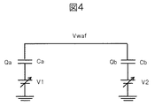
また、静電吸着電極の電位も図3(b)に示すように変化がないため、ウエハと静電吸着電極との間の電位差は、図3(d)に示すように0のままであり、ウエハと電極との間には静電吸着力は発生しない。次に真空処理室内の荷電粒子が完全に消失した後の時刻T3において静電吸着電極に印加している直流電圧を0Vにする。この際、静電吸着電極の電位が変化するが、ウエハの電位も静電吸着電極の電位の変化とほぼ同時に静電吸着電極の電位の変化量と同量の値が変化する。このことについては、図4に示すプラズマ消失後のウエハと静電吸着電極と誘電体層と可変直流電源を含む電気回路の簡略化した等価回路を用いて説明する。尚、図4の等価回路においては、ウエハと静電吸着電極との間の誘電体膜の抵抗値は十分に大きいとし、静電容量のみを考慮する。 Moreover, since the potential of the electrostatic adsorption electrode does not change as shown in FIG. 3B, the potential difference between the wafer and the electrostatic adsorption electrode remains 0 as shown in FIG. 3D. No electrostatic attraction force is generated between the wafer and the electrode. Next, at time T3 after the charged particles in the vacuum processing chamber have completely disappeared, the DC voltage applied to the electrostatic attraction electrode is set to 0V. At this time, the potential of the electrostatic adsorption electrode changes, but the potential of the wafer also changes at the same amount as the amount of change in the potential of the electrostatic adsorption electrode almost simultaneously with the change in the potential of the electrostatic adsorption electrode. This will be described using a simplified equivalent circuit of an electric circuit including a wafer after plasma disappearance, an electrostatic attraction electrode, a dielectric layer, and a variable DC power supply shown in FIG. In the equivalent circuit of FIG. 4, it is assumed that the resistance value of the dielectric film between the wafer and the electrostatic attraction electrode is sufficiently large, and only the capacitance is considered.
図4のCaおよびCbは、誘電体層の静電容量値、QaおよびQbは、静電容量に蓄積された電荷、V1およびV2は、可変直流電源の電圧値である。また、ウエハ電位をVwafとすると図4に示す等価回路においては以下の式1が成り立つ。
In FIG. 4, Ca and Cb are capacitance values of the dielectric layer, Qa and Qb are charges accumulated in the capacitance, and V1 and V2 are voltage values of the variable DC power supply. Further, when the wafer potential is Vwaf, the following

尚、ここで、Qa=―Qbであるので、Qa=―Qb=Qとするとウエハ電位は以下の式2となる。
Since Qa=-Qb, the wafer potential is expressed by the
ここでCa=Cbであれば、ウエハの電位は以下の式3となる。
Here, if Ca=Cb, the potential of the wafer is given by
従って、V1をV1+ΔV1、V2をV2+ΔV2のように静電吸着電極の電位を変化させたとすると、ウエハ電位の変化量ΔVwafは以下の式4となる。
Therefore, if the potential of the electrostatic attraction electrode is changed such that V1 is V1+ΔV1 and V2 is V2+ΔV2, the wafer potential change amount ΔVwaf is given by the
従って、内側静電吸着電極108の電位と外側静電吸着電極109の電位との平均値をΔV分シフトさせると、ウエハの電位もΔVシフトすることとなる。また、容量のみが支配的である場合、この変化は即座に起こる。
Therefore, when the average value of the potential of the inner
上述のように時刻T3においては、静電吸着電極の電位とウエハの電位が同じタイミングで等しい量変化することになるため、図3(d)に示すように時刻T3においてもウエハと静電吸着電極の間の電位差は0に保たれる。すなわち、ウエハと静電吸着電極の間に作用する静電吸着力を0にした状態で静電吸着電極の電位を0Vとすることができる。前記のように静電吸着電極の電位を0Vにした後、ウエハは押し上げピンによって試料台から離脱され、搬送機構(図示せず)によって処理室外部へ搬出される。 As described above, at time T3, the potential of the electrostatic attraction electrode and the potential of the wafer change by the same amount at the same timing. Therefore, as shown in FIG. The potential difference between the electrodes is kept at zero. That is, the potential of the electrostatic attraction electrode can be set to 0 V in a state where the electrostatic attraction force acting between the wafer and the electrostatic attraction electrode is zero. After the electric potential of the electrostatic adsorption electrode is set to 0 V as described above, the wafer is detached from the sample table by the push-up pin and carried out to the outside of the processing chamber by the transfer mechanism (not shown).
次に除電プラズマ中のウエハ電位について述べる。除電プラズマ中のウエハ電位は、除電プラズマ中の浮遊電位と等しいと考えられる。発明者が実施したプラズマ浮遊電位計測の結果を図5に示す。図5(a)に浮遊電位のマイクロ波パワー依存性を示し、図5(b)に浮遊電位の圧力依存性を示す。プラズマ処理時のマイクロ波パワー、圧力に対して浮遊電位の依存性は大きく無く、プラズマ処理条件の変化に対して浮遊電位の変化は比較的感度が低いことが図5から伺える。浮遊電位は、平均して−15V程度のため、この−15Vがウエハの電位として補正すべき量となる。値のばらつきに関しては、浮遊電位の絶対値は、−12Vから−18Vの間に入っているため、マージンを考慮して−15V±5Vが妥当であると考えられる。このようなことから、本実施例においての図3のΔVは、−10からー20Vまでの値とした。 Next, the wafer potential in the static elimination plasma will be described. The wafer potential in the static elimination plasma is considered to be equal to the floating potential in the static elimination plasma. The results of plasma floating potential measurement performed by the inventor are shown in FIG. 5A shows the microwave power dependence of the floating potential, and FIG. 5B shows the pressure dependence of the floating potential. It can be seen from FIG. 5 that the dependency of the floating potential on the microwave power and pressure during the plasma processing is not so large and the change in the floating potential is relatively insensitive to the change in the plasma processing conditions. The floating potential is about -15 V on average, and this -15 V is the amount to be corrected as the potential of the wafer. Regarding the variation of the value, the absolute value of the floating potential is between −12 V and −18 V, so that it is considered that −15 V±5 V is appropriate considering the margin. For this reason, ΔV in FIG. 3 in this example is set to a value from −10 to −20V.
次に、プラズマ生成用のマイクロ波電力が遮断された後の、真空処理室内の荷電粒子消失の待ち時間tについて述べる。 Next, the waiting time t for the disappearance of charged particles in the vacuum processing chamber after the microwave power for plasma generation is cut off will be described.
荷電粒子消失待ち時間tは、前述の通りプラズマ生成用のマイクロ波電力の遮断後、真空処理室内からプラズマによって生成された荷電粒子が完全に消失するまでの時間であるが、真空処理室内からの荷電粒子の消失は、プラズマ中の荷電粒子密度や真空処理室内の圧力など、処理室内の状態のみならず、マイクロ波電源やマイクロ波発振源の制御信号に対する応答性やその応答時間ばらつき等にも影響を受ける可能性がある。 The charged particle disappearance waiting time t is the time until the charged particles generated by the plasma in the vacuum processing chamber completely disappear after the microwave power for plasma generation is cut off as described above. The disappearance of charged particles depends not only on the state of the inside of the processing chamber, such as the density of charged particles in the plasma and the pressure inside the vacuum processing chamber, but also on the response to control signals from the microwave power source and microwave oscillation source, and variations in its response time. May be affected.
このような影響を排除できるように荷電粒子消失待ち時間tは、十分な時間が確保される必要がある。一方、荷電粒子消失待ち時間tを長くすることは、除電という観点からは問題がないが、余分な荷電粒子消失待ち時間はスループットの悪化につながり好ましくない。このようなことから発明者の実験によれば、様々な条件において荷電粒子消失待ち時間tを検討したところ、0.1秒以上の待ち時間があれば、真空処理室内の荷電粒子が消失するのに十分であるとの結果が得られた。また、荷電粒子消失待ち時間としての上限については、スループットに問題のない範囲として3秒とした。また、荷電粒子消失を待つことは、マイクロ波電力遮断後のアフターグロー放電の消失を待つことと同様のことであるため、アフターグロー放電消失待ち時間も0.1〜3秒までの時間としても良い。 In order to eliminate such an influence, it is necessary to secure a sufficient time for the waiting time t of disappearing charged particles. On the other hand, increasing the waiting time t for disappearing charged particles causes no problem from the viewpoint of static elimination, but the extra waiting time for disappearing charged particles leads to deterioration in throughput and is not preferable. From the above, according to the experiments by the inventor, when the waiting time t for disappearing charged particles was examined under various conditions, it was found that the charged particles in the vacuum processing chamber disappeared if there was a waiting time of 0.1 seconds or more. The result was obtained. Further, the upper limit of the waiting time for disappearance of charged particles was set to 3 seconds as a range in which there is no problem in throughput. Since waiting for the disappearance of charged particles is the same as waiting for the disappearance of afterglow discharge after microwave power cutoff, the afterglow discharge disappearance waiting time may be 0.1 to 3 seconds. good.
次に図3のT1において内側静電吸着電極108と外側静電吸着電極109のそれぞれに印加される電圧が異なる実施例について図6に示すタイミングチャートを用いて図3の実施例と異なる構成の部分を説明する。マイクロ波の入射パワーを図6(a)、静電吸着用電極の電位を図6(b)、静電吸着電極の電位の平均値を図6(c)、ウエハの電位を図6(d)、静電吸着用電極とウエハとの電位差を図6(e)にそれぞれ示す。また、図6における、T0、T1、T2、T3、t及びΔVは、図3の同記号と同様の意味で用いている。
Next, regarding the embodiment in which the voltages applied to the inner
図6においては、除電プラズマ発生中時刻T1にて内側の可変直流電源110の出力電圧値がVa、外側の可変直流電源111の出力電圧値がVbに設定される。この際、VaおよびVbの平均値は図6(c)に示すようにウエハの電位と等しい値、すなわち、図3における-ΔVとなる。時刻T1においては内側静電吸着電極とウエハとの間、外側静電吸着電極とウエハとの間には図6(e)に示すようにそれぞれ電位差が発生するため、この時点ではウエハと静電吸着電極との間の吸着力は消失していない。
In FIG. 6, the output voltage value of the variable
その後、時刻T2においてプラズマ生成のための高周波電力(マイクロ波入射パワー)を遮断する。前記高周波電力の遮断後、所定の時間tが経過した後、真空処理室内の荷電粒子が完全に消失する。その後、時刻T3において内側静電吸着電極108及び外側静電吸着電極109のそれぞれに印加している直流電圧を0Vにする。時刻T3において静電吸着電極に印加している直流電圧を0Vにすることにより、内側静電吸着電極108と外側静電吸着電極109に印加している直流電圧の平均値は、図6(c)に示すように−ΔVから0Vに+ΔVだけ変化する。
After that, at time T2, the high frequency power (microwave incident power) for plasma generation is shut off. After a predetermined time t has passed after the high frequency power was cut off, the charged particles in the vacuum processing chamber completely disappeared. After that, at time T3, the DC voltage applied to each of the inner
これは、式3に示すようにウエハの電位変化は、内側静電吸着電極108と外側静電吸着電極109のそれぞれに印加している直流電圧の平均値の変化と等しいため、ウエハ電位は図6(d)に示すように時刻T3において−ΔVから0Vに変化することによる。すなわち、時刻T3において、内側静電吸着電極108の電位と外側静電吸着電極109の電位とウエハの電位が全て0Vとなり、図6(e)に示すようにウエハと静電吸着電極との間の電位差が速やかに解消され、ウエハと静電吸着電極との間に作用する静電吸着力は消失する。
This is because the change in the wafer potential is equal to the change in the average value of the DC voltage applied to each of the inner
図6に示すようなウエハ離脱方法によっても図3のウエハ離脱方法と同様の効果が得られ、残留吸着力の発生なく試料台からの試料離脱を安定して行うことができる。 The wafer releasing method as shown in FIG. 6 has the same effect as that of the wafer releasing method in FIG. 3, and the sample can be stably released from the sample stage without the generation of residual suction force.
以上、本発明を実施の形態に基づいて具体的に説明したが、本発明は前記実施の形態に限定されず、その要旨を逸脱しない範囲で種々に変更可能である。例えば、本実施例においては内側静電吸着電極108と外側静電吸着電極109のそれぞれに印加する直流電源の電圧値はそれぞれ等しいもの、もしくは正と負の異なる電位としたが、内側静電吸着電極108と外側静電吸着電極109のそれぞれに印加する直流電源の電圧値は両者の平均値が−ΔVになれば、どのような値であってもよい。すなわち、静電吸着電極への可変直流電源による−ΔVとして平均−15Vの印加を行なう場合、内側静電吸着電極108に印加する電圧が−5V、外側静電吸着電極109に印加する電圧が-25Vなどの設定であってもよい。また、静電吸着電極への可変直流電源による−ΔVとして平均−15Vの印加を行なう場合、内側静電吸着電極108に印加する電圧が+5V、外側静電吸着電極109に印加する電圧が-35Vなどの設定であってもよい。
Although the present invention has been specifically described above based on the embodiments, the present invention is not limited to the above embodiments and can be variously modified without departing from the scope of the invention. For example, in the present embodiment, the voltage values of the DC power supplies applied to the inner
また、図3及び図6に示すような本発明に係る制御は、制御部115によって行われる。さらに本実施例は、双極型(ダイポール)の静電吸着電極を用いて説明したが、単極型(モノポール)の静電吸着電極にも本発明は適用できる。
The control according to the present invention as shown in FIGS. 3 and 6 is performed by the
また、本実施例では、−ΔVをウエハ電位(浮遊電位)と同等の電位として説明したが、−ΔVを図3及び6のT3におけるウエハ電位が概ね0となる値としても良い。ノイズ等の外乱により−ΔVを浮遊電位にした場合、T3におけるウエハ電位が概ね0とならない場合が有り得るが、−ΔVをT3におけるウエハ電位が概ね0となる値にした場合は、確実にT3時のウエハ電位は概ね0となる利点がある。 Further, in the present embodiment, −ΔV is described as a potential equivalent to the wafer potential (floating potential), but −ΔV may be a value at which the wafer potential at T3 in FIGS. When −ΔV is set to a floating potential due to a disturbance such as noise, the wafer potential at T3 may not be substantially 0. However, when −ΔV is set to a value at which the wafer potential at T3 is substantially 0, it is ensured that at T3 time. Has the advantage that the wafer potential is almost zero.
以上、本発明は、試料台からの試料の離脱に際し、処理中の試料吸着の解除に伴い静電吸着電極に印加する電圧の平均値を、試料を離脱させるためのプラズマ処理の終了後の残留電荷を想定し所定の負電位に設定し、試料を離脱させるためのプラズマ処理の終了後に静電吸着電極への電圧印加を0Vとすることにより、プラズマ消失時の再帯電の恐れなく、ウエハ電位と電極の電位との両方を0Vにすることができるため、残留吸着力の発生なく試料台からの試料離脱を安定して行うことができる。 As described above, when the sample is removed from the sample stage, the average value of the voltage applied to the electrostatic adsorption electrode due to the release of the sample adsorption during the processing is determined by the residual value after the plasma processing for releasing the sample. By setting a predetermined negative potential assuming the charge and applying a voltage of 0 V to the electrostatic adsorption electrode after the plasma treatment for separating the sample is completed, there is no fear of recharging at the time of plasma disappearance, and the wafer potential is reduced. Since both of the potential of the electrode and the potential of the electrode can be set to 0 V, the sample can be stably released from the sample stage without the generation of the residual adsorption force.
101…処理室、102…試料台、103…ウエハ、104…ソレノイドコイル、105…マイクロ波電源、106…マイクロ波発振源、107…導波管、108…静電吸着電極、109…静電吸着電極、110…可変直流電源、111…可変直流電源、112…誘電体層、113…通過孔、114…押し上げピン、115…制御部 101... Processing chamber, 102... Sample stage, 103... Wafer, 104... Solenoid coil, 105... Microwave power source, 106... Microwave oscillation source, 107... Waveguide, 108... Electrostatic adsorption electrode, 109... Electrostatic adsorption Electrode, 110... Variable DC power supply, 111... Variable DC power supply, 112... Dielectric layer, 113... Passage hole, 114... Push-up pin, 115... Control part
Claims (10)
前記試料のプラズマ処理後、前記高周波電力を第一の高周波電力から第二の高周波電力に変更させ、
前記第二の高周波電力が供給されている間の所定の時、前記直流電圧を前記プラズマ処理時の値から所定の値に変更させ、
前記第二の高周波電力の供給が停止された後、前記直流電圧を前記所定の値から概0Vに変更させ、
前記直流電圧が概0Vに変更された後、プラズマ処理された前記試料を前記試料台から離脱させる制御を行う制御部をさらに備え、
前記第二の高周波電力は、前記試料台に静電吸着した前記試料を前記試料台から離脱させるためのプラズマを生成するための高周波電力であり、
前記所定の値は、前記所定の時における前記電極の電位が前記試料の電位と概ね同等となるようにして求められた値であることを特徴とするプラズマ処理装置。 A processing chamber in which a sample is plasma-processed, a high-frequency power source for supplying high-frequency power for generating plasma, a sample stage on which the sample is mounted, the electrode for electrostatically adsorbing the sample, and In a plasma processing apparatus comprising a DC power supply for applying a DC voltage to the electrodes,
After the plasma treatment of the sample, the high frequency power is changed from the first high frequency power to the second high frequency power,
At a predetermined time while the second high-frequency power is being supplied, the DC voltage is changed from the value during the plasma processing to a predetermined value,
After the supply of the second high frequency power is stopped, the DC voltage is changed from the predetermined value to approximately 0V,
And a control unit that controls the plasma-treated sample to be separated from the sample stage after the DC voltage is changed to approximately 0V.
The second high-frequency power is a high-frequency power for generating plasma for detaching the sample electrostatically adsorbed on the sample stage from the sample stage,
The plasma processing apparatus, wherein the predetermined value is a value obtained such that the potential of the electrode at the predetermined time is substantially equal to the potential of the sample.
前記電極が2個の場合、前記一方の電極に印加される第一の直流電圧と前記他方の電極に印加される第二の直流電圧の平均値が前記所定の値となるようにして求められた前記第一の直流電圧および前記第二の直流電圧が前記電極の各々に印加されることを特徴とするプラズマ処理装置。 The plasma processing apparatus according to claim 1,
When the number of the electrodes is two, the average value of the first DC voltage applied to the one electrode and the second DC voltage applied to the other electrode is determined to be the predetermined value. A plasma processing apparatus, wherein the first DC voltage and the second DC voltage are applied to each of the electrodes.
前記プラズマ処理時の値と前記所定の値との差における絶対値は、前記第二の高周波電力により生成されたプラズマの浮遊電位の絶対値と概ね同等であることを特徴とするプラズマ処理装置。 The plasma processing apparatus according to claim 1 or 2,
A plasma processing apparatus, wherein an absolute value of a difference between the plasma processing value and the predetermined value is substantially equal to an absolute value of a floating potential of plasma generated by the second high frequency power.
前記所定の値は、−20〜−10Vの範囲内の値であることを特徴とプラズマ処理装置。 The plasma processing apparatus according to claim 1,
The plasma processing apparatus is characterized in that the predetermined value is a value within a range of -20 to -10V.
前記第二の高周波電力の供給を停止してから所定時間が経過した後、前記直流電圧を前記所定の値から概0Vに変更させ、
前記所定時間は、0.1〜3秒の範囲内の時間であることを特徴とするプラズマ処理装置。 The plasma processing apparatus according to claim 1,
After a lapse of a predetermined time from stopping the supply of the second high frequency power, the DC voltage is changed from the predetermined value to about 0V,
The plasma processing apparatus, wherein the predetermined time is within a range of 0.1 to 3 seconds.
前記試料をプラズマ処理した後、プラズマを生成するための高周波電力を第一の高周波電力から第二の高周波電力に変更し、
前記第二の高周波電力を供給している間の所定の時、前記試料を前記試料台に静電吸着させるための直流電圧を前記プラズマ処理時の値から所定の値に変更し、
前記第二の高周波電力の供給を停止した後、前記直流電圧を前記所定の値から概0Vに変更し、
前記直流電圧を概0Vに変更した後、プラズマ処理された前記試料を前記試料台から離脱させ、
前記第二の高周波電力は、前記試料台に静電吸着した前記試料を前記試料台から離脱させるためのプラズマを生成するための高周波電力であり、
前記所定の値は、前記所定の時における前記電極の電位が前記試料の電位と概ね同等となるようにして求められた値であることを特徴とする試料の離脱方法。 A sample detaching method of detaching the electrostatically adsorbed sample from the sample stage after the sample placed on the sample stage having an electrode for electrostatically adsorbing the sample is plasma-treated. At
After plasma processing the sample, changing the high frequency power for generating plasma from the first high frequency power to the second high frequency power,
At a predetermined time while supplying the second high-frequency power, the direct current voltage for electrostatically adsorbing the sample to the sample stage is changed from the value during the plasma treatment to a predetermined value,
After stopping the supply of the second high frequency power, the DC voltage is changed from the predetermined value to approximately 0V,
After changing the DC voltage to approximately 0 V, the plasma-treated sample is detached from the sample stage,
The second high-frequency power is high-frequency power for generating plasma for separating the sample electrostatically adsorbed on the sample stage from the sample stage,
The predetermined value is a value obtained such that the electric potential of the electrode at the predetermined time is substantially equal to the electric potential of the sample.
前記電極が2個の場合、前記一方の電極に印加される第一の直流電圧と前記他方の電極に印加される第二の直流電圧の平均値が前記所定の値となるようにして求められた前記第一の直流電圧および前記第二の直流電圧を前記電極の各々に印加することを特徴とする試料の離脱方法。 The method for removing a sample according to claim 6,
When the number of the electrodes is two, the average value of the first DC voltage applied to the one electrode and the second DC voltage applied to the other electrode is calculated so as to be the predetermined value. A method for removing a sample, characterized in that the first DC voltage and the second DC voltage are applied to each of the electrodes.
前記プラズマ処理時の値と前記所定の値との差における絶対値は、前記第二の高周波電力により生成されたプラズマの浮遊電位の絶対値と概ね同等であることを特徴とする試料の離脱方法。 The method for separating a sample according to claim 6 or 7,
The absolute value of the difference between the value at the time of the plasma treatment and the predetermined value is substantially equal to the absolute value of the floating potential of the plasma generated by the second high frequency power. ..
前記所定の値は、−20〜−10Vの範囲内の値であることを特徴と試料の離脱方法。 The method for removing a sample according to claim 6,
The predetermined value is a value within a range of -20 to -10V, and a method of separating a sample.
前記第二の高周波電力の供給を停止してから所定時間が経過した後、前記直流電圧を前記所定の値から概0Vに変更し、
前記所定時間は、0.1〜3秒の範囲内の時間であることを特徴とする試料の離脱方法。 The method for removing a sample according to claim 6,
After a lapse of a predetermined time from stopping the supply of the second high frequency power, the DC voltage is changed from the predetermined value to about 0V,
The said predetermined time is a time within the range of 0.1 to 3 seconds, The sample detachment method characterized by the above-mentioned.
Priority Applications (5)
| Application Number | Priority Date | Filing Date | Title |
|---|---|---|---|
| JP2016152424A JP6708358B2 (en) | 2016-08-03 | 2016-08-03 | Plasma processing apparatus and sample separation method |
| KR1020170004058A KR101883246B1 (en) | 2016-08-03 | 2017-01-11 | Plasma processing apparatus and method for separating sample |
| TW106102962A TWI660422B (en) | 2016-08-03 | 2017-01-25 | Plasma processing device and method for removing sample |
| US15/425,155 US10825700B2 (en) | 2016-08-03 | 2017-02-06 | Plasma processing apparatus and method for releasing sample |
| US17/038,072 US20210013060A1 (en) | 2016-08-03 | 2020-09-30 | Plasma processing apparatus and method for releasing sample |
Applications Claiming Priority (1)
| Application Number | Priority Date | Filing Date | Title |
|---|---|---|---|
| JP2016152424A JP6708358B2 (en) | 2016-08-03 | 2016-08-03 | Plasma processing apparatus and sample separation method |
Publications (3)
| Publication Number | Publication Date |
|---|---|
| JP2018022756A JP2018022756A (en) | 2018-02-08 |
| JP2018022756A5 JP2018022756A5 (en) | 2018-11-22 |
| JP6708358B2 true JP6708358B2 (en) | 2020-06-10 |
Family
ID=61072045
Family Applications (1)
| Application Number | Title | Priority Date | Filing Date |
|---|---|---|---|
| JP2016152424A Active JP6708358B2 (en) | 2016-08-03 | 2016-08-03 | Plasma processing apparatus and sample separation method |
Country Status (4)
| Country | Link |
|---|---|
| US (2) | US10825700B2 (en) |
| JP (1) | JP6708358B2 (en) |
| KR (1) | KR101883246B1 (en) |
| TW (1) | TWI660422B (en) |
Families Citing this family (4)
| Publication number | Priority date | Publication date | Assignee | Title |
|---|---|---|---|---|
| JP7059064B2 (en) * | 2018-03-26 | 2022-04-25 | 株式会社日立ハイテク | Plasma processing equipment |
| CN112885691A (en) * | 2019-11-29 | 2021-06-01 | 中微半导体设备(上海)股份有限公司 | Plasma processing apparatus and method for optimizing stability thereof |
| JP2021118353A (en) | 2020-01-29 | 2021-08-10 | 東京エレクトロン株式会社 | Board processing method and board processing system |
| JP7350995B2 (en) * | 2021-02-25 | 2023-09-26 | 株式会社日立ハイテク | plasma processing equipment |
Family Cites Families (19)
| Publication number | Priority date | Publication date | Assignee | Title |
|---|---|---|---|---|
| TW334609B (en) | 1996-09-19 | 1998-06-21 | Hitachi Ltd | Electrostatic chuck, method and device for processing sanyle use the same |
| KR19980024679U (en) * | 1996-10-30 | 1998-07-25 | 홍성기 | Commercial cassette tape |
| US5933314A (en) * | 1997-06-27 | 1999-08-03 | Lam Research Corp. | Method and an apparatus for offsetting plasma bias voltage in bi-polar electro-static chucks |
| JPH11111826A (en) * | 1997-10-02 | 1999-04-23 | Sumitomo Metal Ind Ltd | Method for separating sample in electrostatic chuck |
| JPH11233605A (en) * | 1998-02-17 | 1999-08-27 | Mitsubishi Electric Corp | Electrostatic chuck stage |
| GB9812850D0 (en) * | 1998-06-16 | 1998-08-12 | Surface Tech Sys Ltd | A method and apparatus for dechucking |
| US6057244A (en) * | 1998-07-31 | 2000-05-02 | Applied Materials, Inc. | Method for improved sputter etch processing |
| US20030236004A1 (en) * | 2002-06-24 | 2003-12-25 | Applied Materials, Inc. | Dechucking with N2/O2 plasma |
| JP2004047511A (en) * | 2002-07-08 | 2004-02-12 | Tokyo Electron Ltd | Method for releasing, method for processing, electrostatic attracting device, and treatment apparatus |
| US7292428B2 (en) * | 2005-04-26 | 2007-11-06 | Applied Materials, Inc. | Electrostatic chuck with smart lift-pin mechanism for a plasma reactor |
| JP2007073568A (en) * | 2005-09-05 | 2007-03-22 | Hitachi High-Technologies Corp | Plasma treatment apparatus |
| US8207701B2 (en) * | 2006-10-31 | 2012-06-26 | Byd Company, Ltd. | Control method of electromotor |
| JP4847909B2 (en) | 2007-03-29 | 2011-12-28 | 東京エレクトロン株式会社 | Plasma processing method and apparatus |
| US8780522B2 (en) * | 2008-07-07 | 2014-07-15 | Lam Research Corporation | Capacitively-coupled electrostatic (CCE) probe arrangement for detecting dechucking in a plasma processing chamber and methods thereof |
| JP6013740B2 (en) * | 2012-02-03 | 2016-10-25 | 東京エレクトロン株式会社 | Detachment control method and control device for plasma processing apparatus |
| JP6132497B2 (en) * | 2012-09-12 | 2017-05-24 | 東京エレクトロン株式会社 | Detachment control method and plasma processing apparatus |
| JP2015072825A (en) * | 2013-10-03 | 2015-04-16 | 株式会社日立ハイテクノロジーズ | Plasma processing device and plasma processing method |
| JP6357436B2 (en) | 2014-07-25 | 2018-07-11 | 株式会社日立ハイテクノロジーズ | Plasma processing equipment |
| US10535566B2 (en) * | 2016-04-28 | 2020-01-14 | Taiwan Semiconductor Manufacturing Company, Ltd. | Semiconductor device and method of manufacture |
-
2016
- 2016-08-03 JP JP2016152424A patent/JP6708358B2/en active Active
-
2017
- 2017-01-11 KR KR1020170004058A patent/KR101883246B1/en active IP Right Grant
- 2017-01-25 TW TW106102962A patent/TWI660422B/en active
- 2017-02-06 US US15/425,155 patent/US10825700B2/en active Active
-
2020
- 2020-09-30 US US17/038,072 patent/US20210013060A1/en active Pending
Also Published As
| Publication number | Publication date |
|---|---|
| JP2018022756A (en) | 2018-02-08 |
| US20210013060A1 (en) | 2021-01-14 |
| KR20180015558A (en) | 2018-02-13 |
| US20180040491A1 (en) | 2018-02-08 |
| US10825700B2 (en) | 2020-11-03 |
| KR101883246B1 (en) | 2018-08-30 |
| TW201816883A (en) | 2018-05-01 |
| TWI660422B (en) | 2019-05-21 |
Similar Documents
| Publication | Publication Date | Title |
|---|---|---|
| US20220139678A1 (en) | Plasma processing apparatus | |
| JP6708358B2 (en) | Plasma processing apparatus and sample separation method | |
| JP5372419B2 (en) | Plasma processing apparatus and plasma processing method | |
| KR102001018B1 (en) | Method for detaching sample and plasma processing device | |
| JP6407694B2 (en) | Plasma processing equipment | |
| US9953854B2 (en) | Method of adsorbing target object on mounting table and plasma processing apparatus | |
| JP6169136B2 (en) | ESC charge control apparatus and method for wafer fixation | |
| JP2007208302A (en) | Plasma processing method and plasma processing device | |
| JP6727068B2 (en) | Plasma processing apparatus and plasma processing method | |
| JP2011040658A (en) | Workpiece holding apparatus, method of controlling electrostatic chuck, and method of manufacturing semiconductor device | |
| CN107546168B (en) | Wafer adsorption method, lower electrode system and semiconductor processing device | |
| JP2009141014A (en) | Plasma processing apparatus and processing method | |
| US11923229B2 (en) | Plasma processing method and plasma processing apparatus | |
| KR102277822B1 (en) | Apparatus for treating substrate | |
| JP6763061B2 (en) | Plasma processing equipment | |
| CN113948359B (en) | Electrostatic chuck and semiconductor processing equipment | |
| JP2000077510A (en) | Electrostatic chuck and method thereof, and plasma etching device provided therewith | |
| KR20210097621A (en) | Substrate processing method and substrate processing system | |
| KR20220091388A (en) | Plasma processing apparatus and plasma processing method | |
| JPH07240457A (en) | Plasma reactor |
Legal Events
| Date | Code | Title | Description |
|---|---|---|---|
| A521 | Request for written amendment filed |
Free format text: JAPANESE INTERMEDIATE CODE: A523 Effective date: 20160805 |
|
| A521 | Request for written amendment filed |
Free format text: JAPANESE INTERMEDIATE CODE: A523 Effective date: 20161213 |
|
| RD04 | Notification of resignation of power of attorney |
Free format text: JAPANESE INTERMEDIATE CODE: A7424 Effective date: 20170120 |
|
| RD04 | Notification of resignation of power of attorney |
Free format text: JAPANESE INTERMEDIATE CODE: A7424 Effective date: 20170126 |
|
| RD02 | Notification of acceptance of power of attorney |
Free format text: JAPANESE INTERMEDIATE CODE: A7422 Effective date: 20170803 |
|
| RD04 | Notification of resignation of power of attorney |
Free format text: JAPANESE INTERMEDIATE CODE: A7424 Effective date: 20170804 |
|
| A521 | Request for written amendment filed |
Free format text: JAPANESE INTERMEDIATE CODE: A523 Effective date: 20181010 |
|
| A621 | Written request for application examination |
Free format text: JAPANESE INTERMEDIATE CODE: A621 Effective date: 20181010 |
|
| A131 | Notification of reasons for refusal |
Free format text: JAPANESE INTERMEDIATE CODE: A131 Effective date: 20190625 |
|
| A977 | Report on retrieval |
Free format text: JAPANESE INTERMEDIATE CODE: A971007 Effective date: 20190628 |
|
| A601 | Written request for extension of time |
Free format text: JAPANESE INTERMEDIATE CODE: A601 Effective date: 20190822 |
|
| A521 | Request for written amendment filed |
Free format text: JAPANESE INTERMEDIATE CODE: A523 Effective date: 20191018 |
|
| A131 | Notification of reasons for refusal |
Free format text: JAPANESE INTERMEDIATE CODE: A131 Effective date: 20200317 |
|
| A521 | Request for written amendment filed |
Free format text: JAPANESE INTERMEDIATE CODE: A523 Effective date: 20200324 |
|
| TRDD | Decision of grant or rejection written | ||
| A01 | Written decision to grant a patent or to grant a registration (utility model) |
Free format text: JAPANESE INTERMEDIATE CODE: A01 Effective date: 20200421 |
|
| A61 | First payment of annual fees (during grant procedure) |
Free format text: JAPANESE INTERMEDIATE CODE: A61 Effective date: 20200519 |
|
| R150 | Certificate of patent or registration of utility model |
Ref document number: 6708358 Country of ref document: JP Free format text: JAPANESE INTERMEDIATE CODE: R150 |