JP6357436B2 - Plasma processing equipment - Google Patents
Plasma processing equipment Download PDFInfo
- Publication number
- JP6357436B2 JP6357436B2 JP2015046627A JP2015046627A JP6357436B2 JP 6357436 B2 JP6357436 B2 JP 6357436B2 JP 2015046627 A JP2015046627 A JP 2015046627A JP 2015046627 A JP2015046627 A JP 2015046627A JP 6357436 B2 JP6357436 B2 JP 6357436B2
- Authority
- JP
- Japan
- Prior art keywords
- plasma
- wafer
- potential
- electrode
- plasma processing
- Prior art date
- Legal status (The legal status is an assumption and is not a legal conclusion. Google has not performed a legal analysis and makes no representation as to the accuracy of the status listed.)
- Active
Links
- 238000012545 processing Methods 0.000 title claims description 234
- 230000001603 reducing effect Effects 0.000 claims description 13
- 208000028659 discharge Diseases 0.000 description 76
- 239000000523 sample Substances 0.000 description 41
- 238000001179 sorption measurement Methods 0.000 description 40
- 238000000034 method Methods 0.000 description 24
- 238000005259 measurement Methods 0.000 description 23
- 230000000694 effects Effects 0.000 description 19
- 238000012795 verification Methods 0.000 description 19
- 238000012360 testing method Methods 0.000 description 16
- 230000008569 process Effects 0.000 description 15
- 230000008859 change Effects 0.000 description 14
- 239000000463 material Substances 0.000 description 14
- 238000005530 etching Methods 0.000 description 11
- 239000004020 conductor Substances 0.000 description 8
- 230000007246 mechanism Effects 0.000 description 8
- 238000003672 processing method Methods 0.000 description 8
- 239000007789 gas Substances 0.000 description 7
- 238000002360 preparation method Methods 0.000 description 7
- 238000003860 storage Methods 0.000 description 7
- 239000004065 semiconductor Substances 0.000 description 6
- 239000000126 substance Substances 0.000 description 6
- 230000009467 reduction Effects 0.000 description 4
- 238000003556 assay Methods 0.000 description 3
- 238000004364 calculation method Methods 0.000 description 3
- 230000007423 decrease Effects 0.000 description 3
- 238000004519 manufacturing process Methods 0.000 description 3
- 239000002245 particle Substances 0.000 description 3
- 238000001020 plasma etching Methods 0.000 description 3
- 230000010356 wave oscillation Effects 0.000 description 3
- 238000013459 approach Methods 0.000 description 2
- 239000000112 cooling gas Substances 0.000 description 2
- 230000006866 deterioration Effects 0.000 description 2
- 238000010586 diagram Methods 0.000 description 2
- 239000000428 dust Substances 0.000 description 2
- 230000010355 oscillation Effects 0.000 description 2
- 238000009832 plasma treatment Methods 0.000 description 2
- 239000000758 substrate Substances 0.000 description 2
- 241001640117 Callaeum Species 0.000 description 1
- 230000032683 aging Effects 0.000 description 1
- 239000000470 constituent Substances 0.000 description 1
- 230000008034 disappearance Effects 0.000 description 1
- 238000005516 engineering process Methods 0.000 description 1
- 150000002500 ions Chemical class 0.000 description 1
- 239000002184 metal Substances 0.000 description 1
- 238000012986 modification Methods 0.000 description 1
- 230000004048 modification Effects 0.000 description 1
- 238000006386 neutralization reaction Methods 0.000 description 1
- 230000001846 repelling effect Effects 0.000 description 1
- 230000003252 repetitive effect Effects 0.000 description 1
Images


Classifications
-
- H—ELECTRICITY
- H01—ELECTRIC ELEMENTS
- H01L—SEMICONDUCTOR DEVICES NOT COVERED BY CLASS H10
- H01L21/00—Processes or apparatus adapted for the manufacture or treatment of semiconductor or solid state devices or of parts thereof
- H01L21/02—Manufacture or treatment of semiconductor devices or of parts thereof
- H01L21/04—Manufacture or treatment of semiconductor devices or of parts thereof the devices having potential barriers, e.g. a PN junction, depletion layer or carrier concentration layer
- H01L21/18—Manufacture or treatment of semiconductor devices or of parts thereof the devices having potential barriers, e.g. a PN junction, depletion layer or carrier concentration layer the devices having semiconductor bodies comprising elements of Group IV of the Periodic Table or AIIIBV compounds with or without impurities, e.g. doping materials
- H01L21/30—Treatment of semiconductor bodies using processes or apparatus not provided for in groups H01L21/20 - H01L21/26
- H01L21/302—Treatment of semiconductor bodies using processes or apparatus not provided for in groups H01L21/20 - H01L21/26 to change their surface-physical characteristics or shape, e.g. etching, polishing, cutting
- H01L21/306—Chemical or electrical treatment, e.g. electrolytic etching
- H01L21/3065—Plasma etching; Reactive-ion etching
-
- H—ELECTRICITY
- H01—ELECTRIC ELEMENTS
- H01J—ELECTRIC DISCHARGE TUBES OR DISCHARGE LAMPS
- H01J37/00—Discharge tubes with provision for introducing objects or material to be exposed to the discharge, e.g. for the purpose of examination or processing thereof
- H01J37/32—Gas-filled discharge tubes
- H01J37/32431—Constructional details of the reactor
- H01J37/32532—Electrodes
-
- H—ELECTRICITY
- H01—ELECTRIC ELEMENTS
- H01J—ELECTRIC DISCHARGE TUBES OR DISCHARGE LAMPS
- H01J37/00—Discharge tubes with provision for introducing objects or material to be exposed to the discharge, e.g. for the purpose of examination or processing thereof
- H01J37/32—Gas-filled discharge tubes
- H01J37/32009—Arrangements for generation of plasma specially adapted for examination or treatment of objects, e.g. plasma sources
- H01J37/32082—Radio frequency generated discharge
- H01J37/32137—Radio frequency generated discharge controlling of the discharge by modulation of energy
- H01J37/32146—Amplitude modulation, includes pulsing
-
- H—ELECTRICITY
- H01—ELECTRIC ELEMENTS
- H01J—ELECTRIC DISCHARGE TUBES OR DISCHARGE LAMPS
- H01J37/00—Discharge tubes with provision for introducing objects or material to be exposed to the discharge, e.g. for the purpose of examination or processing thereof
- H01J37/32—Gas-filled discharge tubes
- H01J37/32431—Constructional details of the reactor
- H01J37/32697—Electrostatic control
- H01J37/32706—Polarising the substrate
-
- H—ELECTRICITY
- H01—ELECTRIC ELEMENTS
- H01J—ELECTRIC DISCHARGE TUBES OR DISCHARGE LAMPS
- H01J37/00—Discharge tubes with provision for introducing objects or material to be exposed to the discharge, e.g. for the purpose of examination or processing thereof
- H01J37/32—Gas-filled discharge tubes
- H01J37/32917—Plasma diagnostics
- H01J37/32935—Monitoring and controlling tubes by information coming from the object and/or discharge
-
- H—ELECTRICITY
- H01—ELECTRIC ELEMENTS
- H01J—ELECTRIC DISCHARGE TUBES OR DISCHARGE LAMPS
- H01J37/00—Discharge tubes with provision for introducing objects or material to be exposed to the discharge, e.g. for the purpose of examination or processing thereof
- H01J37/32—Gas-filled discharge tubes
- H01J37/32917—Plasma diagnostics
- H01J37/3299—Feedback systems
-
- H—ELECTRICITY
- H05—ELECTRIC TECHNIQUES NOT OTHERWISE PROVIDED FOR
- H05H—PLASMA TECHNIQUE; PRODUCTION OF ACCELERATED ELECTRICALLY-CHARGED PARTICLES OR OF NEUTRONS; PRODUCTION OR ACCELERATION OF NEUTRAL MOLECULAR OR ATOMIC BEAMS
- H05H1/00—Generating plasma; Handling plasma
- H05H1/24—Generating plasma
- H05H1/46—Generating plasma using applied electromagnetic fields, e.g. high frequency or microwave energy
Landscapes
- Physics & Mathematics (AREA)
- Engineering & Computer Science (AREA)
- Plasma & Fusion (AREA)
- Chemical & Material Sciences (AREA)
- Analytical Chemistry (AREA)
- General Physics & Mathematics (AREA)
- Spectroscopy & Molecular Physics (AREA)
- Condensed Matter Physics & Semiconductors (AREA)
- Electromagnetism (AREA)
- Manufacturing & Machinery (AREA)
- Computer Hardware Design (AREA)
- Microelectronics & Electronic Packaging (AREA)
- Power Engineering (AREA)
- Drying Of Semiconductors (AREA)
- Plasma Technology (AREA)
- Container, Conveyance, Adherence, Positioning, Of Wafer (AREA)
Description
本発明は、半導体装置の製造の技術に関する。また本発明は、半導体装置の製造に好適なプラズマ処理装置に関する。 The present invention relates to a technique for manufacturing a semiconductor device. The present invention also relates to a plasma processing apparatus suitable for manufacturing a semiconductor device.
半導体装置の製造におけるプラズマ処理方法の一つにプラズマエッチングがある。プラズマエッチングは、プラズマ処理室内の載置台上に搬入された半導体基板であるウェハの積層膜をプラズマに暴露することにより、ウェハに微細な回路パターンを形成する。この際、プラズマ処理の対象の膜の種類によって、プラズマ処理の諸条件、即ちガス種、圧力、およびプラズマ発生のための電力値、等が異なる。そのため、ある膜の処理が終了した後、次の膜の処理のために、プラズマ処理の条件を切り替える必要がある。このプラズマ処理の条件および対応する処理の切り替えの間は、安定しないため、意図しないエッチングの進行を防止するために、プラズマ放電を中断することが一般的である。 One of plasma processing methods in the manufacture of semiconductor devices is plasma etching. Plasma etching forms a fine circuit pattern on a wafer by exposing a laminated film of a wafer, which is a semiconductor substrate carried on a mounting table in a plasma processing chamber, to plasma. At this time, various conditions of the plasma processing, that is, gas type, pressure, power value for generating plasma, and the like vary depending on the type of the film to be subjected to plasma processing. Therefore, after the processing of a certain film is completed, it is necessary to switch the plasma processing conditions for the processing of the next film. Since this plasma processing condition and the corresponding processing switching are not stable, it is common to interrupt the plasma discharge in order to prevent unintended etching progress.
上記プラズマ放電の中断を伴うプラズマ処理および条件の切り替えに関して、プラズマの消失により処理室内の塵埃がウェハに付着することが指摘されている。以下、塵埃を異物と記載する。特にウェハに電位が与えられている場合、異物がクーロン力によりウェハに引き寄せられ付着することがある。ウェハに異物が付着すると、異物がエッチングを阻害し、歩留まりの悪化を招く。 Regarding the plasma processing and the switching of conditions with the interruption of the plasma discharge, it has been pointed out that dust in the processing chamber adheres to the wafer due to the disappearance of the plasma. Hereinafter, dust is referred to as foreign matter. In particular, when a potential is applied to the wafer, foreign matter may be attracted and attached to the wafer by Coulomb force. If foreign matter adheres to the wafer, the foreign matter inhibits etching, leading to a decrease in yield.
上記プラズマ処理におけるウェハへ付着する異物の低減に関する先行技術例として、以下が挙げられる。 The following are examples of prior art relating to the reduction of foreign matter adhering to the wafer in the plasma treatment.
特開2001−15581号公報(特許文献1)には、プラズマ処理室の内部の異物の多くが負に帯電しているとし、単極型吸着電極を用いてウェハを処理室内の保持台に吸着する際、電極に負の電位を与えて吸着することで、ウェハに負の電位を付与する旨が開示されている。 In Japanese Patent Laid-Open No. 2001-15581 (Patent Document 1), it is assumed that most of the foreign matters inside the plasma processing chamber are negatively charged, and the wafer is adsorbed to a holding table in the processing chamber using a monopolar adsorption electrode. In this case, it is disclosed that a negative potential is applied to the wafer by applying a negative potential to the electrode for adsorption.
一方、特開2003−100720号公報(特許文献2)には、異物が正に帯電しているとし、負の電位が付与される異物除去電極により異物を吸着する旨が開示されている。 On the other hand, Japanese Patent Laid-Open No. 2003-100720 (Patent Document 2) discloses that a foreign substance is adsorbed by a foreign substance removing electrode to which a negative potential is applied, assuming that the foreign substance is positively charged.
また、特開2002−270576号公報(特許文献3)には、プラズマ処理を行っていない間には、単極型吸着用電極の電源出力を遮断し、ウェハに電位を与えないことで、異物がウェハに引き寄せられることを防止する旨が開示されている。 Japanese Patent Laid-Open No. 2002-270576 (Patent Document 3) discloses that foreign matter can be obtained by shutting off the power output of the unipolar adsorption electrode and applying no potential to the wafer while plasma processing is not performed. Is disclosed to prevent the wafer from being attracted to the wafer.
特許文献1および特許文献2の技術は、異物の大半が正極性もしくは負極性に帯電している状況を想定している。そのため、処理室内に正負の両方の異物が存在する場合には、異物のウェハへの付着の低減効果が期待できない。
The techniques of
また特許文献3の技術は、異物源となる処理室の内壁面の電位について考慮されていない。プラズマ処理を行う処理室の内壁面は、プラズマにさらされることになるため、プラズマからの荷電粒子の流入により帯電し、電位を持つ場合がある。処理室の内壁面に電位を持つ場合、ウェハと内壁面との間に電位差が発生することになるため、帯電した異物がウェハへ引き寄せられる可能性がある。 The technique of Patent Document 3 does not take into account the potential of the inner wall surface of the processing chamber that is a foreign material source. Since the inner wall surface of the processing chamber in which the plasma processing is performed is exposed to the plasma, it may be charged by the inflow of charged particles from the plasma and have a potential. When the inner wall surface of the processing chamber has a potential, a potential difference is generated between the wafer and the inner wall surface, so that charged foreign substances may be attracted to the wafer.
さらに、ウェハと処理室の内壁面との間に意図しない電位差を発生させる要因として、ウェハを載置台上に吸着するための電極である静電吸着電極の構造や経年劣化が挙げられる。クーロン力によるウェハへの異物の付着に関して、静電吸着電極の動作等は、大きな影響を及ぼす。 Furthermore, as a factor that causes an unintended potential difference between the wafer and the inner wall surface of the processing chamber, there are a structure of an electrostatic adsorption electrode that is an electrode for adsorbing the wafer onto the mounting table, and aging deterioration. The operation of the electrostatic chucking electrode has a great influence on the adhesion of foreign matter to the wafer due to the Coulomb force.
本発明の目的は、上記プラズマ処理に関して、処理および条件の切り替えに伴うプラズマ放電の中断中に、ウェハと処理室の内壁面との間に意図しない電位差が発生することを抑制し、帯電した異物のウェハへの付着を低減できる技術を提供することである。 An object of the present invention is to suppress the occurrence of an unintended potential difference between the wafer and the inner wall surface of the processing chamber during the interruption of the plasma discharge associated with the switching of the processing and conditions in the plasma processing, and charged foreign matter It is to provide a technique capable of reducing the adhesion of the wafer to the wafer.
本発明のうち代表的な実施の形態は、プラズマ処理装置であって、以下に示す構成を有することを特徴とする。 A typical embodiment of the present invention is a plasma processing apparatus having the following configuration.
一実施の形態のプラズマ処理装置は、プラズマを用いて試料がプラズマ処理されるプラズマ処理室と、前記プラズマを生成するための高周波電力を供給する高周波電源と、前記プラズマ処理室内に配置され前記試料を載置する試料台と、前記試料台の内部に配置され前記試料を静電吸着させるための電極と、前記電極に直流電圧を印加する直流電源と、
前記プラズマが不存在の場合における、前記試料の電位と前記プラズマ処理室の内壁の電位との電位差を低減させる前記直流電圧の値として求められた値を前記電極に印加するように前記直流電源を制御する制御装置とを備える。
In one embodiment, a plasma processing apparatus includes: a plasma processing chamber in which a sample is plasma-processed using plasma; a high-frequency power supply that supplies high-frequency power for generating the plasma; and the sample disposed in the plasma processing chamber A sample table, an electrode disposed inside the sample table for electrostatically adsorbing the sample, a DC power source for applying a DC voltage to the electrode,
In the absence of the plasma, the DC power supply is applied so that a value obtained as a value of the DC voltage for reducing the potential difference between the potential of the sample and the inner wall of the plasma processing chamber is applied to the electrode. And a control device for controlling.
一実施の形態のプラズマ処理装置は、プラズマを用いて試料がプラズマ処理されるプラズマ処理室と、前記プラズマを生成するための高周波電力を供給する高周波電源と、前記プラズマ処理室内に配置され前記試料を載置する試料台と、前記試料台の内部に配置され前記試料を静電吸着させるための電極と、前記電極に直流電圧を印加する直流電源と、前記プラズマが不存在であるとともに前記プラズマ処理室の内壁の電位が略0である場合の前記試料の電位を低減させる前記直流電圧の値として求められた値を前記電極に印加するように前記直流電源を制御する制御装置とを備える。 In one embodiment, a plasma processing apparatus includes: a plasma processing chamber in which a sample is plasma-processed using plasma; a high-frequency power supply that supplies high-frequency power for generating the plasma; and the sample disposed in the plasma processing chamber A sample stage, an electrode disposed inside the sample stage for electrostatically adsorbing the sample, a direct current power source for applying a direct current voltage to the electrode, the plasma being absent and the plasma And a control device that controls the DC power supply so that a value obtained as a value of the DC voltage for reducing the potential of the sample when the potential of the inner wall of the processing chamber is substantially 0 is applied to the electrode.
一実施の形態のプラズマ処理装置において、前記電極は、プラスの直流電圧が印加される第一の電極と、マイナスの直流電圧が印加される第二の電極と、を有し、前記直流電源は、前記第一の電極へ直流電圧を印加する第一の直流電源と、前記第二の電極へ直流電圧を印加する第二の直流電源と、を有する。 In the plasma processing apparatus of one embodiment, the electrode has a first electrode to which a positive DC voltage is applied and a second electrode to which a negative DC voltage is applied, and the DC power source is , A first DC power source for applying a DC voltage to the first electrode, and a second DC power source for applying a DC voltage to the second electrode.
一実施の形態のプラズマ処理装置において、前記所定の範囲は、±10Vである。 In the plasma processing apparatus of one embodiment, the predetermined range is ± 10V.
本発明のうち代表的な実施の形態によれば、上記プラズマ処理に関して、処理の切り替えに伴うプラズマ放電の中断中に、ウェハと処理室内壁面との間に意図しない電位差が発生することを抑制し、帯電した異物のウェハへの付着を低減できる。 According to a typical embodiment of the present invention, an unintended potential difference is suppressed between the wafer and the processing chamber wall surface during the plasma discharge interruption due to the process switching. The adhesion of charged foreign matter to the wafer can be reduced.
以下、本発明の実施の形態を図面に基づいて詳細に説明する。なお実施の形態を説明するための全図において同一部には原則として同一符号を付しその繰り返しの説明は省略する。また、各実施形態の説明において、「放電」と「プラズマ」が混在しているが、同義語として「放電」と「プラズマ」を使用している。 Hereinafter, embodiments of the present invention will be described in detail with reference to the drawings. Note that components having the same function are denoted by the same reference symbols throughout the drawings for describing the embodiment, and the repetitive description thereof will be omitted. In the description of each embodiment, “discharge” and “plasma” are mixed, but “discharge” and “plasma” are used as synonyms.
<概要等>
背景技術および課題について補足説明しつつ、本実施の形態の概要等を説明する。従来、プラズマ処理および条件の切り替えの際には、例えば数秒から十数秒の時間がかかる。使用するガスの切り替えの場合、前処理で使用されたガスを処理室から排気し、次処理で使用するガスを処理室内に充填するための時間が必要とされる。
<Summary>
An outline of the present embodiment and the like will be described while supplementally explaining background technology and problems. Conventionally, for plasma processing and switching of conditions, for example, it takes several seconds to tens of seconds. In the case of switching the gas to be used, time is required for exhausting the gas used in the pretreatment from the processing chamber and filling the processing chamber with the gas used in the next processing.
処理室における静電吸着電極とウェハとは、その間に存在する誘電体層によって有限の抵抗値および静電容量値を持って電気的に接続される。静電吸着電極は、クーロン力によってウェハを吸着する。静電吸着電極は、単極型のものと多極型のものとがある。多極型のもののうち、電極が二枚のものを、特に双極型と記載する。 The electrostatic adsorption electrode and the wafer in the processing chamber are electrically connected with a finite resistance value and a capacitance value by a dielectric layer existing between them. The electrostatic adsorption electrode adsorbs the wafer by Coulomb force. The electrostatic adsorption electrode includes a monopolar type and a multipolar type. Among the multipolar type, those having two electrodes are particularly described as a bipolar type.
単極型の電極は、電極に与えられた電位がウェハの電位に影響する。単極型の電極は、例えば正の電位が与えられてウェハを吸着すると、プラズマ放電を行っていない場合、ウェハには正の電位が現れる。 In a monopolar electrode, the potential applied to the electrode affects the potential of the wafer. For example, when a positive potential is applied to a monopolar electrode and the wafer is attracted, a positive potential appears on the wafer when plasma discharge is not performed.
一方、双極型の電極は、各々の電極に逆極性の電位が付与されてウェハを吸着する。その際、ウェハの電位は、理想的には両電極に付与された電位の平均値となるように設計される場合が多い。例えば一方の電極に+500V、他方の電極に−500Vの電位が付与された場合、ウェハの電位は0Vになる。一方の電極に+600V、他方の電極に−400Vの電位が付与された場合、ウェハの電位は+100Vになる。 On the other hand, the bipolar electrode attracts the wafer by applying a potential of opposite polarity to each electrode. At that time, the potential of the wafer is ideally designed to be an average value of potentials applied to both electrodes in many cases. For example, when a potential of +500 V is applied to one electrode and −500 V is applied to the other electrode, the potential of the wafer is 0 V. When a potential of +600 V is applied to one electrode and −400 V is applied to the other electrode, the potential of the wafer is +100 V.
ウェハと処理室の内壁面との間に意図しない電位差を発生させる要因として、静電吸着電極の構造上の問題や経年劣化が挙げられる。例えば、双極型電極での吸着の場合、二枚の電極の面積が異なる場合や、ウェハの載置台上に異物等が付着することによって二枚の各電極とウェハとの間のそれぞれの抵抗値に差が生じる場合がある。これらの場合、二枚の静電吸着電極に付与される電位の平均値を0Vにしても、互いの電極状態の不均一から、ウェハに電位が発生することがあり得る。 Factors that cause an unintended potential difference between the wafer and the inner wall surface of the processing chamber include structural problems of the electrostatic chucking electrode and deterioration over time. For example, in the case of adsorption with a bipolar electrode, the resistance value between each of the two electrodes and the wafer when the areas of the two electrodes are different or when foreign matter adheres on the wafer mounting table. There may be differences. In these cases, even if the average value of the potential applied to the two electrostatic adsorption electrodes is set to 0 V, a potential may be generated on the wafer due to the non-uniformity of the mutual electrode state.
上記静電吸着電極を含む影響により、プラズマ放電の中断中に、ウェハと処理室の内壁面との間に、ある程度以上に大きな電位差が発生する。これにより、処理室内の帯電した異物がクーロン力によりウェハへ引き寄せられて付着することがある。 Due to the influence including the electrostatic adsorption electrode, a potential difference larger than a certain level is generated between the wafer and the inner wall surface of the processing chamber during the interruption of the plasma discharge. As a result, charged foreign matter in the processing chamber may be attracted and adhered to the wafer by Coulomb force.
本発明の実施の形態のプラズマ処理装置は、プラズマ処理および条件の切り替えに伴うプラズマ放電の中断中に、上記静電吸着電極を含む影響により、ウェハと処理室の内壁面との間に意図しない電位差が発生することを抑制する仕組みを有する。これにより、処理室内の帯電した異物がクーロン力によりウェハへ引き寄せられて付着することを低減する。 The plasma processing apparatus according to the embodiment of the present invention is not intended between the wafer and the inner wall surface of the processing chamber due to the influence including the electrostatic adsorption electrode during the interruption of the plasma discharge accompanying the plasma processing and switching of conditions. It has a mechanism to suppress the occurrence of potential difference. Thereby, the charged foreign matter in the processing chamber is reduced from being attracted to and attached to the wafer by the Coulomb force.
<実施の形態1>
図1〜図5を用いて、本発明の実施の形態1のプラズマ処理装置について説明する。
<
The plasma processing apparatus according to the first embodiment of the present invention will be described with reference to FIGS.
[プラズマ処理装置]
図1は、実施の形態1のプラズマ処理装置の要部断面の構成を示す。図1の実施の形態1のプラズマ処理装置は、電子サイクロトロン共鳴型エッチング装置である。以下、電子サイクロトロン共鳴をECRと記載する。本発明に係るプラズマ処理装置は、ECR型エッチング装置に限らず適用可能である。
[Plasma processing equipment]
FIG. 1 shows a cross-sectional configuration of the main part of the plasma processing apparatus of the first embodiment. The plasma processing apparatus of the first embodiment shown in FIG. 1 is an electron cyclotron resonance type etching apparatus. Hereinafter, electron cyclotron resonance is referred to as ECR. The plasma processing apparatus according to the present invention is not limited to an ECR type etching apparatus and can be applied.
図1のECR型エッチング装置であるプラズマ処理装置は、真空処理室である処理室101の内部の試料台である載置台102上に、試料となる半導体基板であるウェハ103が載置され、処理室101の内部にプラズマを発生させる。
The plasma processing apparatus which is the ECR type etching apparatus of FIG. 1 has a
プラズマ処理装置は、プラズマ発生後、載置台102の内部に設置された高周波電極104に、高周波電源105から電力を供給する。当該電力の供給により、ウェハ103には、自己バイアスと呼ばれる負の電位が発生する。この負の電位によってイオンをウェハ103に引き込むことにより、いわゆる反応性イオンエッチングが起こり、エッチング処理が進行する。
The plasma processing apparatus supplies power from the high
処理室101の内壁基材は、接地された導体が含まれている。実施の形態1では、上記接地された導体が含まれる内壁基材である導体内壁基材は、プラズマに暴露されていてもよい。また当該導体内壁基材は、プラズマ消失後に当該内壁表面が速やかにおおよそ0Vとなる程度の薄い誘電体の膜があってもよい。101aは、処理室101の内壁面、および上記導体内壁基材を示す。101bは、内壁面101aに関する接地を示す。
The inner wall base material of the
プラズマ処理装置は、プラズマを発生させる機構として、μ波発振源106およびソレノイドコイル107を備える。μ波発振源106で発生させたμ波は、導波管108を介して処理室101に導入される。μ波は、ソレノイドコイル107で発生させた磁場中でECRによって電子にエネルギーを与える。その電子が、図示しないガス供給源から供給されたガスを電離させることによって、プラズマを発生させる。
The plasma processing apparatus includes a μ-
上記プラズマ処理を行う間、ウェハ103の裏面には、当該ウェハ103の温度の調整のための冷却ガスが供給される。冷却ガスによるウェハ103のずれを防ぐために、ウェハ103は、双極型の静電吸着電極109,110によって、載置台102上に吸着される。静電吸着電極109,110は、同心円状に、一方の電極である静電吸着電極109が内側、他方の電極である静電吸着電極110が外側に配置されている。静電吸着電極109,110とウェハ103との間には、誘電体層111が存在している。静電吸着電極109,110とウェハ103は、有限の抵抗値と静電容量を持って電気的に接続される。
During the plasma treatment, a cooling gas for adjusting the temperature of the
静電吸着用電極109,110は、それぞれ、独立した直流電源である可変直流電源112,113が接続される。内側の静電吸着用電極109には、一方の可変直流電源112が接続され、外側の静電吸着用電極110には、他方の可変直流電源113が接続される。
静電吸着用電極109,110には、それぞれの電源により、逆極性の電位が付与される。例えば内側の静電吸着電極109には、可変直流電源112により+500Vの電位が付与され、外側の静電吸着電極110には、可変直流電源113により−500Vの電位が付与される。
The
A reverse polarity potential is applied to the
また、実施の形態1のプラズマ処理装置は、上記可変直流電源112,113の出力電圧値を制御するための制御装置115および記憶装置114を備える。可変直流電源112,113は、制御装置115と接続され、制御装置115から出力電圧値が制御される。
Further, the plasma processing apparatus of the first embodiment includes a
実施の形態1において、静電吸着電極109,110とウェハ103との間の誘電体層111は、ある程度のリーク電流が流れる程度の抵抗率となっている。例えば、誘電体層111が、Johnsen−Rahbek効果によって吸着を行うための溶射膜である場合、上記のようなリーク電流が流れる。なお、Johnsen−Rahbek効果とは、金属表面と半導体表面との間に電位差を付与することで吸着力が発生する現象であり、静電吸着の一方式としてしばしば用いられる。
In the first embodiment, the
[等価回路]
図2は、実施の形態1のプラズマ処理装置における、可変直流電源112,113、静電吸着電極109,110、誘電体層111、およびウェハ103を簡単にモデル化した等価回路を示す。なお、この等価回路では、ウェハ103の抵抗は無視できるほど小さいとする。図2の等価回路で、V1は可変直流電源112の電圧、V2は可変直流電源113の電圧である。R1,R2は、誘電体層111の抵抗、C1,C2は、誘電体層111の容量である。R1,C1は、一方の静電吸着電極109側の抵抗と容量、R2,C2は、他方の静電吸着電極110側の抵抗と容量である。
[Equivalent circuit]
FIG. 2 shows an equivalent circuit in which the variable
プラズマ放電が行われていない時の定常状態におけるウェハ103の電位であるVwafを、下記の式1に示す。式1で、R1,R2は上記誘電体層111の抵抗の抵抗値、V1,V2は、上記可変直流電源112,113の出力電圧値を示す。
Vwaf , which is the potential of the

従って、式1でR1=R2の場合、ウェハ103の電位は、両電源である可変直流電源112,113の出力電圧値であるV1,V2の平均値となる。
Therefore, when R 1 = R 2 in
一方、何らかの理由で抵抗値にずれが生じ、式1でR1≠R2となった場合、ウェハ103の電位は、両電源の出力電圧値の平均値とならず、ウェハ103には、意図しない電位が付与されることとなる。ウェハ103に意図しない電位が付与される場合、ウェハ103と処理室101の内壁面101aとの間の電位差によって帯電した異物が、ウェハ103に誘引される恐れがある。処理室101の内壁面101aは、異物の発生源の一つである。
On the other hand, if the resistance value shifts for some reason and R 1 ≠ R 2 in Equation 1, the potential of the
ウェハ103に意図しない電位を発生させないために、実施の形態1のプラズマ処理装置は、ウェハ103に付与される電位が所望の値となるように、上記抵抗値であるR1,R2の値に応じて、可変直流電源112,113の出力電圧値であるV1,V2を制御する。
In order not to generate an unintended potential on the
実施の形態1では、処理室101の内壁面101aの基材は接地された導体であり、その表面の接地抵抗値および対地静電容量が十分小さいとしている。従って、プラズマ放電中断中の処理室101の内壁面101aの電位は、放電終了後、比較的速やかにおよそ0Vになる。そのため、ウェハ103と処理室101の内壁面101aとの間に電位差を発生させないためには、ウェハ103の電位を0V程度にすればよい。
In the first embodiment, the base material of the
ウェハ103の電位が0Vになる可変直流電源112と可変直流電源113との出力電圧の比は、式1から、以下の式2となる。
The ratio of the output voltages of the variable
実施の形態1のプラズマ処理装置は、プラズマ処理および条件の切り替えに伴うプラズマ放電中断中に、静電吸着用電極109,110に接続される可変直流電源112,113の出力電圧であるV1,V2を、上記式2を満たすように変化させる。これにより、実施の形態1のプラズマ処理装置は、ウェハ103の電位を0Vにし、ウェハ103と処理室101の内壁面101aとの電位差を発生させないようにする。
The plasma processing apparatus of the first embodiment is configured to output V 1 , which are output voltages of the variable
[処理タイムチャート]
図3は、プラズマ処理装置におけるプラズマ処理を含む従来の処理の様子を示すタイムチャートである。このプラズマ処理装置は、処理室101の構成は図1と同様とするが、実施の形態1の制御装置115によりプラズマ放電中断中に静電吸着用電極109,110への出力電圧を制御する仕組みを持たない構成の場合である。
[Processing time chart]
FIG. 3 is a time chart showing the state of conventional processing including plasma processing in the plasma processing apparatus. In this plasma processing apparatus, the configuration of the
図3の(a)は、μ波入射パワーを示し、μ波発振源106からのμ波電力である。(b)は、高周波バイアス入射パワーを示し、高周波電源105からの高周波電極104への電力である。(c)は、可変直流電源出力電圧を示す。実線の301は内側の静電吸着電極109への可変直流電源112の出力電圧、破線の302は外側の静電吸着電極110への可変直流電源113の出力電圧を示す。この一実施の形態では、当該出力電圧は、可変の制御はされずに一定である。(d)は、ウェハ電位および内壁面電位を示す。実線の311はウェハ103の電位、破線の312は処理室101の内壁面101aの電位を示す。時刻t0からt1の時間T1は、プラズマ放電中の時間を示す。時刻t1からt2の時間T2は、プラズマ放電中断中の時間を示す。
FIG. 3A shows the μ wave incident power, which is the μ wave power from the μ
図3の従来の形態での処理の場合、(d)の放電中断中の時間T2に、ウェハ電位である311aと内壁面電位である312aとの間に、313に示すような電位差が発生する。この電位差により、異物がウェハ103へ引き寄せられて付着する可能性がある。
In the case of the processing in the conventional form of FIG. 3, a potential difference as shown by 313 occurs between the wafer potential 311a and the inner wall surface potential 312a at the time T2 during the discharge interruption of (d). . Due to this potential difference, foreign matter may be attracted and attached to the
図4は、実施の形態1のプラズマ処理装置におけるプラズマ処理を含む処理の様子を図3と同様に示すタイムチャートである。図4の(a)は、μ波入射パワーを示し、μ波発振源106からのμ波電力である。(b)は、高周波バイアス入射パワーを示し、高周波電源105からの高周波電極104への電力である。(c)は、可変直流電源出力電圧を示す。実線の401は内側の静電吸着電極109への可変直流電源112の出力電圧、破線の402は外側の静電吸着電極110への可変直流電源113の出力電圧を示す。実施の形態1では、当該出力電圧は、可変に制御される。(d)は、ウェハ電位および内壁面電位を示す。実線の411はウェハ103の電位、破線の412は処理室101の内壁面101aの電位を示す。
FIG. 4 is a time chart showing the state of the processing including the plasma processing in the plasma processing apparatus of the first embodiment, similar to FIG. FIG. 4A shows the μ wave incident power, which is the μ wave power from the μ
実施の形態1のプラズマ処理装置において、ウェハ103が試料台である載置台102上に載置された後、制御装置115からの制御に基づいて、可変直流電源112および可変直流電源113は、ウェハ103の吸着のための所定の電圧を出力する。プラズマ処理装置は、その後、処理室101の内部の圧力調整等の処理の準備を行う。当該準備については図示を省略する。
In the plasma processing apparatus of the first embodiment, after the
上記準備が終了した後、(a)のように、時刻t0から、プラズマ発生のための所定のμ波電力が印加される。これによりプラズマが発生した後、放電中の時間T1において、(b)のように、高周波バイアスが印加されて、エッチング処理が行われる。所望のエッチング処理が終了すると、(b)で、まず高周波バイアス入射パワーが遮断される。当該遮断により、(d)で、時刻t1に示すように、ウェハ103の電位である411と、内壁面101aの電位である412とは、ほぼ同程度となる。
After the preparation is completed, a predetermined μ-wave power for plasma generation is applied from time t0 as shown in (a). Thus, after the plasma is generated, at time T1 during discharge, as shown in (b), a high frequency bias is applied to perform an etching process. When the desired etching process is completed, the high frequency bias incident power is first cut off in (b). By the interruption, as shown at time t1 in (d), the potential 411 of the
その後、(a)で、放電中断中の時間T2において、μ波入射パワーの供給が停止し、次の処理の準備のためにプラズマ放電が中断される。 Thereafter, in (a), at the time T2 during the interruption of the discharge, the supply of the μ wave incident power is stopped, and the plasma discharge is interrupted in preparation for the next processing.
時刻t1で示すプラズマ放電終了の瞬間には、処理室101の内壁面101aは、プラズマからの電子流入により帯電しており、(d)の412のように、ある程度の電位を持っている。この電位は、処理室101の内壁面101aに溜まった電荷がアースへと抜ける時定数に従って変化していく。実施の形態1では、この時定数は短く、処理室101の内壁面101aの電位は、412aに示すように、比較的速やかに0Vになるとする。
At the moment of the end of the plasma discharge indicated at time t1, the
また時刻t1で、ウェハ103の電位に関しても、ある程度のリーク電流が流れるため、プラズマからの荷電粒子の流入による帯電で発生した電位は比較的速く消失し、抵抗値の内外差等によって現れる電極個別の特性に応じた電位となる。
Further, at time t1, a certain amount of leakage current also flows with respect to the potential of the
このため、例えば前述のR1≠R2の場合、図3の一実施の形態のプラズマ処理装置の処理の場合では、(d)に示すように、放電中断中の時間T2では、時間T2で、内壁面101aの電位は、312aのように0Vになるが、ウェハ103の電位は、311aのように、0Vにはならない。即ち、ウェハ103と内壁面101aとの間に、313に示す電位差が発生することになる。
For this reason, for example, in the case of R 1 ≠ R 2 described above, in the case of the processing of the plasma processing apparatus of the embodiment of FIG. 3, as shown in FIG. The potential of the
これに対して、図4の実施の形態1のプラズマ処理装置の処理では、制御装置115による、(c)の可変直流電源112および可変直流電源113の出力電圧の可変の制御を行う。(c)の400は、この可変直流電源112および可変直流電源113の出力電圧の変化およびその時間を示す。
On the other hand, in the processing of the plasma processing apparatus of the first embodiment in FIG. 4, the
制御装置115は、(c)の出力電圧の制御により、(d)のように、ウェハ103の電位を変化させる。即ち、制御装置115は、(d)で、放電中の時間T1のウェハ103の電位である411が、放電中断中の時間T2に、411aのように0Vになるように、当該出力電圧を、式2を満たすように変化させる。
The
(c)で、放電中の時間T1では、可変直流電源112の出力電圧である401は、所定の正の電圧であり、可変直流電源113の出力電圧である402は、所定の負の電圧である。制御装置115は、放電中断中の時間T2で、400の時間において、それぞれの所定の出力電圧値に維持する制御を行う。即ち、制御装置115は、可変直流電源112の出力電圧である401を、400の時間に、所定電圧高くなるように変化させて、401aの電圧の状態を維持する。同様に、制御装置115は、可変直流電源113の出力電圧である402を、400の時間に、所定電圧高くなるように変化させて、402aの電圧の状態を維持する。これにより、(d)で、400の時間に、ウェハ103の電位である411aは、内壁面101aの電位である412aと同様に0Vに近付く。
In (c), at time T1 during discharge, 401 which is the output voltage of the variable
実施の形態1のプラズマ処理装置において、上記静電吸着電極109,110への可変直流電源112,113の出力電圧値の変化は、以下により達成される。即ち、記憶装置114は、プラズマ放電中断中の時間T2に出力すべき可変直流電源112,113の出力電圧値を記憶する。制御装置115は、放電中断中の時間T2に、記憶装置114に記憶された出力電圧値になるように、可変直流電源112,113の出力電圧値を可変に制御する。
In the plasma processing apparatus of the first embodiment, the change in the output voltage value of the variable
なお、プラズマ処理装置は、ユーザの操作に基づいて記憶装置114に上記制御の出力電圧値を設定するためのユーザインタフェースを備えてもよい。
The plasma processing apparatus may include a user interface for setting the output voltage value of the control in the
実施の形態1のプラズマ処理装置は、上記制御を含む動作によって、放電中断中の時間T2に、ウェハ103と内壁面101aとの間の電位差を解消する。(d)の400の時間では、411aおよび412aのように、当該電位差がほぼ0Vとなる。これにより、異物がウェハ103に誘引されて付着することが防止される。
The plasma processing apparatus of the first embodiment eliminates the potential difference between the
プラズマ処理装置は、上記制御装置115による制御により時間T2の400で所定の出力電圧を維持したまま、処理室101内の圧力調整等の、次の放電処理のための準備を行う。当該準備が終了した後、プラズマ処理装置は、制御装置115による400での制御を停止する。これにより可変直流電源112,113は、次の放電処理のための所定の電圧、即ち401,402と同じ電圧を出力する。その後、時刻t2から、μ波入射パワーの供給が開始され、次の放電処理が実施される。
The plasma processing apparatus prepares for the next discharge process such as pressure adjustment in the
プラズマ処理装置は、以上のようなプラズマ放電処理および放電中断を含む制御を、最終の放電処理が終了するまで繰り返し、最終の放電処理の終了後には、所定のウェハ除電シーケンスを経て、可変直流電源112,113の電圧を遮断する。 The plasma processing apparatus repeats the control including the plasma discharge process and the discharge interruption as described above until the final discharge process is completed, and after the final discharge process is completed, the variable DC power supply is passed through a predetermined wafer neutralization sequence. The voltages of 112 and 113 are cut off.
[効果等]
上記プラズマ放電中断中にウェハ103と処理室101の内壁面101aとの間の電位差を解消するにあたり、どの程度まで電位差を小さくすれば、異物の付着の低減効果を得るために十分であるかについて、以下のように検討した。
[Effects]
In order to eliminate the potential difference between the
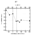
図5は、実施の形態1のプラズマ処理装置における、帯電した異物のウェハ103への付着の低減効果について、計算によって見積もりを行った結果のグラフである。グラフの横軸はウェハ103と処理室101の内壁面101aとの電位差[V]を示す。グラフの縦軸は異物のウェハ103への付着率[%]を示す。
FIG. 5 is a graph showing a result obtained by estimating the effect of reducing the adhesion of charged foreign matter to the
この見積りの計算は、以下の条件で行われた。処理室101内の圧力を0.6Paとし、処理室101内には平均3m/s程度の排気口へ向かうガスの流れがあるものとした。異物は、真空の処理室101の内壁面101aのうちの側面から1000個発生するものとした。異物の発生位置は、大まかな範囲で指定され、1000個の個々の異物の夫々の発生場所については、指定の範囲内でランダムに決定された。異物の粒径は、1000個の異物の夫々について、15nm以上120nm以下の値がランダムに与えられた。異物の初速に関しても、1000個の異物のそれぞれについて、5m/s以下の値がランダムに与えられた。本計算では、帯電した異物をウェハ103に引き寄せる効果について見積もるため、異物の帯電は、1000個の全ての異物で、−1.6×10−19[C]とした。
This estimate was calculated under the following conditions. It was assumed that the pressure in the
上記条件で異物のウェハ103への付着率を計算した。その結果、図5に示すように、ウェハ103と処理室101の内壁面101aとの間の電位差が+10Vである場合、ウェハ103へ付着する異物は2%程度であった。この付着率は、電位差が0Vである場合の付着率との差はあまり無い。しかしながら、ウェハ103と処理室101の内壁面101aとの電位差が+20Vである場合は、付着率が、8%程度まで上昇するという結果が得られた。
The adhesion rate of foreign matter to the
上記結果から、実施の形態1のプラズマ処理装置は、十分な異物の付着の低減効果が得られる、プラズマ放電中断中のウェハ103と内壁面101aとの電位差の目安を、±10V以内とした。図4の(d)で、放電中断中の時間T2の電位差を0Vで示しているが、当該電位差が±10V以内であれば、相応の十分な効果が得られる。
From the above results, in the plasma processing apparatus of the first embodiment, the potential difference between the
上述のように、実施の形態1のプラズマ処理装置およびそのプラズマ処理方法によれば、プラズマ処理および条件の切り替えに伴うプラズマ放電の中断中に、ウェハ103と処理室101の内壁面101aとの間に意図しない電位差が発生することを抑制し、帯電した異物のウェハ103への付着を低減することができる。
As described above, according to the plasma processing apparatus and the plasma processing method of the first embodiment, during the interruption of the plasma discharge accompanying the plasma processing and the switching of the conditions, the gap between the
<実施の形態2>
図6,図7を用いて、本発明の実施の形態2のプラズマ処理装置について説明する。以下、実施の形態2における実施の形態1とは異なる構成の部分について説明する。実施の形態2のプラズマ処理装置は、実施の形態1のプラズマ処理装置における放電中断中の可変直流電源112,113の出力電圧を、ウェハ103の電位と可変直流電源112,113の出力電圧との間の関係を把握するための計測を基に決定する。
<Embodiment 2>
A plasma processing apparatus according to the second embodiment of the present invention will be described with reference to FIGS. In the following, the configuration of the second embodiment different from that of the first embodiment will be described. In the plasma processing apparatus of the second embodiment, the output voltage of the variable
前述の実施の形態1では、ウェハ103の電位を、ウェハ103と静電吸着電極109,110との間の誘電体層111の抵抗値を基に決定する構成を示した。しかしながら、この抵抗値が正確に把握できない場合や、意図しない電位がその他の要因によって発生している場合は、実施の形態1の構成を適用することができない。
In the first embodiment, the configuration in which the potential of the
その場合、実施の形態2の構成を適用することが有効である。実施の形態2では、ウェハ103の電位であるVwafと、可変直流電源112,113の出力電圧値であるV1,V2との間の関係を計測によって把握しておく。これにより、プラズマ放電中断中にウェハ103と処理室101の内壁面101aとの間の電位差を低減させる制御を行うことができる。上記計測による把握を含む作業を、以下、検定と記載する。
In that case, it is effective to apply the configuration of the second embodiment. In the second embodiment, the relationship between V waf that is the potential of the
実施の形態2のプラズマ処理装置は、実施の形態1のプラズマ処理装置と同様の構成要素に加え、上記検定を行うための手段として、実験装置を含む機構を備える。実施の形態2のプラズマ処理装置におけるプラズマ処理方法は、実施の形態1と同様のプラズマ処理装置の構成において、まず上記検定を行う。 The plasma processing apparatus according to the second embodiment includes a mechanism including an experimental apparatus as means for performing the above-described test in addition to the same components as those of the plasma processing apparatus according to the first embodiment. In the plasma processing method in the plasma processing apparatus of the second embodiment, the above test is first performed in the same plasma processing apparatus configuration as that of the first embodiment.
上記検定は、例えば以下のような手段および手順により実現される。実施の形態2のプラズマ処理装置は、ウェハ103の電位の計測が可能な機構を設ける。この機構は、処理室101を大気開放してウェハ103に電位計測プローブを貼り付けること等により実現される。実施の形態2のプラズマ処理装置は、この計測の機構を用いて、制御装置115により可変直流電源112,113の出力電圧を様々に変化させた場合の、ウェハ103の電位を計測する。
The above assay is realized by the following means and procedures, for example. The plasma processing apparatus of the second embodiment is provided with a mechanism that can measure the potential of the
[検定]
図6は、実施の形態2のプラズマ処理装置における、上記実験装置および計測の機構を含む検定の手段を用いて、ウェハ103の電位と、可変直流電源112,113の出力電圧とに関する検定を行った結果の例であるグラフを示す。グラフの横軸は、可変直流電源112,113の出力電圧の平均値[V]である。グラフの縦軸は、ウェハ103の電位[V]である。また、この検定はプラズマを生成しない状態で行った。
[Test]
FIG. 6 shows a calibration of the potential of the
なお、この検定の際、以下の条件とした。出力電圧は、内側の静電吸着電極109の可変直流電源112が+500V、外側の静電吸着電極110の可変直流電源113が−500Vを基準とした。この出力電圧の変化は、可変直流電源112および可変直流電源113の両方で、等しい量で変化させることとした。例えば図6の横軸の可変直流電源の出力電圧の平均値を+10V変化させる場合には、可変直流電源112と可変直流電源113との両方の出力電圧を+10V変化させた。その場合、可変直流電源112の出力電圧は+510V、可変直流電源113の出力電圧は−490Vになる。
In this test, the following conditions were used. The output voltage was based on + 500V for the variable
実施の形態2のプラズマ処理装置は、上記検定の結果、図6のように、可変直流電源112,113の出力電圧の平均値が0Vである場合には、ウェハ103に−40V程度の電位が付与されていた。当該出力電圧の平均値を変化させると、ウェハ103の電位も、当該平均値の変化量とほぼ同量変化した。ウェハ103の電位が0Vになる当該出力電圧の平均値は、+40V程度であった。
In the plasma processing apparatus of the second embodiment, when the average value of the output voltages of the variable
実施の形態2のプラズマ処理装置は、実施の形態1と同様に、プラズマ放電中断中の処理室101の内壁面101aの電位は、放電終了後に比較的速やかにおよそ0Vになる。そのため、実施の形態2のプラズマ処理装置は、制御装置115により、放電中断中、可変直流電源112,113の出力電圧の平均値が+40Vになるように設定する。これにより、図4の(d)のように、ウェハ103と内壁面101aとの電位差を解消できる。
In the plasma processing apparatus of the second embodiment, as in the first embodiment, the potential of the
上記検定によって決定された、プラズマ放電中断中の可変直流電源112,113の出力電圧値を、V1ctrl,V2ctrlとする。図4の401aがV1ctrl,402aがV2ctrlに対応する。記憶装置114は、このV1ctrl,V2ctrlの値を記憶する。プラズマ処理装置は、図4の(c)と同様に、プラズマ放電中断中の時間T2において、制御装置115により、400の時間に、可変直流電源112,113の出力電圧値を、V1ctrl,V2ctrlとなるように制御する。
The output voltage values of the variable
[効果等]
図7は、実施の形態2のプラズマ処理装置における、異物の付着の低減効果として、放電中断中に可変直流電源112,113の出力電圧を様々に変化させた際の、ウェハ103に付着した異物数の変化を表すグラフである。グラフの横軸は、可変直流電源112,113の出力電圧の平均値[V]、およびそれに対応付けられたウェハ103の電位[V]を示す。グラフの縦軸は、ウェハ103に付着した異物数を示す。この異物数は、可変直流電源112,113の出力電圧の平均値が0Vの場合の異物数によって規格化された値を示す。
[Effects]
FIG. 7 shows the foreign matter adhering to the
図7に示すように、可変直流電源112,113の出力電圧の平均値が+40V付近、つまりウェハ103の電位が0V付近になっている場合、従来の通常の運用である可変直流電源112,113の出力電圧の平均値が0Vの場合と比較して、40%程度の異物低減効果が得られた。また、ウェハ103の電位が負極性になる場合には、ウェハ103の電位の絶対値が大きくなる程、ウェハ103に付着する異物数が増加する。一方、ウェハ103の電位が正極性になる場合には、ウェハ103の電位の絶対値が大きくなっても、ウェハ103に付着する異物数は大きくは変化しない。
As shown in FIG. 7, when the average value of the output voltages of the variable
上記結果から、以下の二点が推測される。一点は、処理室101内の帯電した異物の多くが正極性に帯電しているということである。ウェハ103の電位が負極性の場合の付着する異物の増加は、正極性に帯電した異物がウェハ103の電位に引き寄せられたことの結果であると考えられる。
From the above results, the following two points are estimated. One point is that most of the charged foreign matter in the
もう一点は、ウェハ103に異物の帯電と同極性の電位を印加して、ウェハ103に飛来する帯電異物を跳ね返して異物の低減を図るという手法の効果は小さいということである。これは、前述の結果より正極性に帯電した異物の存在が示唆されているにも関わらず、ウェハ103に正極性の電位を付与しても異物の低減効果が得られなかったことから判断される。このことに関しては、放電中断中に発生する異物は、処理室101の内壁面101aから発生する際の初速度が十分小さく、ウェハ103と内壁面101aとの間に電位差が無い場合、ウェハ103まで飛来できる異物が少ない状況であると考えることで説明できる。従って、放電中断中には帯電した異物を不要にウェハ103へ引き寄せることが無いように電位を制御することが肝要であると言える。
Another point is that the effect of the technique of applying a potential having the same polarity as the charge of the foreign matter to the
実施の形態2のプラズマ処理装置は、上記二点を含めて考慮し、放電中断中、帯電した異物を不要にウェハ103へ引き寄せることが無いように、制御装置115により可変直流電源112,113の出力電圧を制御して、ウェハ103の電位を制御する。
The plasma processing apparatus of the second embodiment takes the above two points into consideration, and controls the variable
以上の結果から、実施の形態2のプラズマ処理装置によれば、放電中断中にウェハ103と処理室101の内壁面101aとの間に意図しない電位差が発生することを抑制することで、帯電した異物のウェハ103への付着を低減できることが確認された。
From the above results, according to the plasma processing apparatus of the second embodiment, charging was suppressed by suppressing the occurrence of an unintended potential difference between the
<実施の形態3>
図8,図9を用いて、本発明の実施の形態3のプラズマ処理装置について説明する。以下、実施の形態3における実施の形態1および実施の形態2とは異なる構成の部分について説明する。
<Embodiment 3>
A plasma processing apparatus according to the third embodiment of the present invention will be described with reference to FIGS. Hereinafter, a part of the third embodiment having a configuration different from that of the first and second embodiments will be described.
[プラズマ処理装置]
図8は、実施の形態3のプラズマ処理装置の要部断面の構成を示す。図8の実施の形態3のプラズマ処理装置も、ECR型エッチング装置であるが、ECR型に限らず適用可能である。実施の形態3のプラズマ処理装置は、実施の形態1および実施の形態2のプラズマ処理装置の構成要素に加え、実施の形態2とは異なる検定の手段を備える。実施の形態3における検定の手段は、当該プラズマ処理装置の検定を、処理室101の大気開放を行うこと無く実施するための機構を含む。実施の形態3のプラズマ処理装置におけるプラズマ処理方法は、当該検定の手段を用いて検定を行う手順を含む。
[Plasma processing equipment]
FIG. 8 shows a cross-sectional configuration of the main part of the plasma processing apparatus of the third embodiment. The plasma processing apparatus of Embodiment 3 in FIG. 8 is also an ECR type etching apparatus, but is not limited to the ECR type and can be applied. In addition to the constituent elements of the plasma processing apparatuses of the first embodiment and the second embodiment, the plasma processing apparatus of the third embodiment includes an examination means different from that of the second embodiment. The means for verification in the third embodiment includes a mechanism for performing verification of the plasma processing apparatus without opening the
図8で、実施の形態3のプラズマ処理装置は、上記検定の手段の構成要素として、電流計801,802と、制御装置803とを備える。電流計801,802は、可変直流電源112,113からウェハ103に流れる電流を測定する電流計であり、制御装置803と接続される。制御装置803は、前述の制御装置115の代わりに設けられ、検定の制御の機能を含む。制御装置803は、電流計801,802で測定した電流が互いに等しくなるように、可変直流電源112,113の出力電圧値を制御する。
In FIG. 8, the plasma processing apparatus of the third embodiment includes
電流計801,802は、特に、載置台102における静電吸着電極109,110から誘電体層111を介してウェハ103へ流れる電流を検出する電流計としてもよい。
In particular, the
実施の形態3のプラズマ処理装置は、検定を行う際、処理室101内に、検定のためのプラズマである検定用プラズマ804を発生させる。この検定用プラズマ804のプラズマ放電を、以下、検定放電と記載する。
The plasma processing apparatus of the third embodiment generates a
[等価回路]
図9は、実施の形態3のプラズマ処理装置における、検定放電中における、可変直流電源112,113、静電吸着電極109,110、誘電体層111、ウェハ103、検定用プラズマ804、および真空の処理室101を簡単にモデル化した等価回路を示す。I1は電流計801の電流、I2は電流計802の電流である。I3は、ウェハ103から検定用プラズマ804への電流である。R3は、検定用プラズマ804の抵抗値、C3は、検定用プラズマ804の静電容量値である。R4は、処理室101の内壁面101aの接地抵抗、C4は、処理室101の内壁面101aの対地静電容量である。
[Equivalent circuit]
FIG. 9 shows variable
検定放電中は、ウェハ103と処理室101の内壁面101aとが、検定用プラズマ804によって電気的に接続される。この際、ウェハ103と処理室101の内壁面101aとの間の当該プラズマを介した抵抗値R3および静電容量値C3は、ウェハ103と静電吸着電極109,110との間の抵抗値R1,R2、および静電容量値C1,C2に比べて、それぞれ十分に小さい。
During the verification discharge, the
また、実施の形態3のプラズマ処理装置では、処理室101の内壁面101aの接地抵抗R4および対地静電容量C4も、上記抵抗値R1,R2および静電容量値C1,C2に比べて十分小さい。そのため、ウェハ103の電位は、検定放電中、ほぼ0Vとなる。
In the plasma processing apparatus of the third embodiment, the ground resistance R 4 and the ground capacitance C 4 of the
また、検定用プラズマ804に電流I3が流れることにより、電流計801と電流計802には、異なる電流であるI1とI2が流れる。実施の形態3のプラズマ処理装置は、制御装置803により、これらの両電流の値が等しくなるように、出力電圧値であるV1およびV2を設定する。当該設定により、検定用プラズマ804には、電流I3が流れなくなる。即ち、プラズマ放電が無い場合の等価回路と等しい状態となる。上記のように決まる可変直流電源112,113の出力電圧値であるV1およびV2が、プラズマ放電が無い時もウェハ103の電位が0Vになるような出力電圧であるV1ctrlおよびV2ctrlとなる。
In addition, when the current I 3 flows through the
実施の形態3のプラズマ処理装置は、ウェハ1枚の処理ごと、あるいは1ロットごと等、必要な単位およびタイミングで、検定放電を行う。検定放電の際、まずウェハ103が真空の処理室101内の載置台102に搬入される。ウェハ103は、静電吸着電極109,110によって載置台102に吸着される。この際の吸着電圧は、製品ウェハの処理を行う際に一般的に使用される値に設定される。
The plasma processing apparatus according to the third embodiment performs a test discharge in a necessary unit and timing such as for each wafer processing or for each lot. During the calibration discharge, first, the
プラズマ処理装置は、その後、処理室101内の圧力調整等、検定放電のための準備を行う。当該準備が終了した後、プラズマ処理装置は、プラズマ発生のための所定のμ波電力の印加によりプラズマを発生させる。プラズマ発生後、電流計801,802で電流が計測される。制御装置803は、上記電流計801,802の両電流値であるI1,I2を監視する。制御装置803は、互いの電流値であるI1,I2の差が、当該電流値の絶対値の和に対して、±1%以内になるように、可変直流電源112,113の出力電圧であるV1,V2を制御する。なお当該可変直流電源112,113の出力電圧の変化は、前述と同様に、等しい量で変化させることとする。
Thereafter, the plasma processing apparatus makes preparations for verification discharge such as pressure adjustment in the
制御装置803は、上記制御において、上記電流値の差が当該電流値の絶対値の和の±1%以内になった場合、可変直流電源112,113の出力電圧の制御を停止し、その際の出力電圧値であるV1,V2の値を、記憶装置114に記憶させる。ここで記憶されたV1,V2の値が、上述のV1ctrl,V2ctrlとなる。
In the above control, when the difference between the current values is within ± 1% of the sum of the absolute values of the current values, the
なお、上記検定放電中の可変直流電源112,113の出力電圧の制御を停止する際の条件である、上記電流値の差は、当該電流値の絶対値の和の±1%以内でなくても構わない。ただし、前述のように、ウェハ103と内壁面101aとの電位差を、異物の低減効果が得られるように十分小さくできることが望まれる。
The difference between the current values, which is a condition for stopping the control of the output voltage of the variable
実施の形態3において、上記制御の停止の条件を、上記電流値の差が当該電流値の絶対値の和の±1%以内であることとしたのは、以下の理由による。実施の形態1における静電吸着電極109と静電吸着電極110との間の電位差が1000Vである。この1000Vの電位差に対して、異物の低減効果が得られるウェハ103と内壁面101aとの間の許容される電位差が±10Vである。上記許容される電位差である±10Vは、上記静電吸着電極109と静電吸着電極110との間の電位差である1000Vの±1%である。よって、上記制御の停止の条件として、上記電流値の差が当該電流値の絶対値の和の±1%以内であることとする。
In the third embodiment, the reason for stopping the control is that the difference between the current values is within ± 1% of the sum of the absolute values of the current values for the following reason. The potential difference between the
プラズマ処理装置は、検定後、製品ウェハの処理を行う。プラズマ処理装置は、製品ウェハの処理の際、制御装置803により、プラズマ放電中断中に、可変直流電源112,113の出力電圧値を、前述の図4の(c)と同様に、V1ctrl,V2ctrlとなるように制御する。
The plasma processing apparatus processes the product wafer after the verification. In the processing of the product wafer, the plasma processing apparatus controls the output voltage values of the variable
[効果等]
上述のように、実施の形態3のプラズマ処理装置のプラズマ処理方法によれば、処理室101の大気開放を行うこと無く検定を実施する。そして本プラズマ処理方法によれば、製品ウェハの処理において、プラズマ放電中断中にウェハ103と処理室101の内壁面101aとの間に意図しない電位差が発生することを抑制する。これにより、帯電した異物のウェハ103への付着を低減することができる。
[Effects]
As described above, according to the plasma processing method of the plasma processing apparatus of the third embodiment, the verification is performed without opening the
<実施の形態4>
図10,図11を用いて、本発明の実施の形態4のプラズマ処理装置について説明する。以下、実施の形態4における前述の形態とは異なる構成の部分について説明する。
<Embodiment 4>
A plasma processing apparatus according to the fourth embodiment of the present invention will be described with reference to FIGS. Hereafter, the part of the configuration different from the above-described embodiment in Embodiment 4 will be described.
[プラズマ処理装置]
図10は、実施の形態4のプラズマ処理装置の要部断面の構成を示す。図10の実施の形態4のプラズマ処理装置も、ECR型エッチング装置であるが、ECR型エッチング装置に限らず適用可能である。実施の形態4のプラズマ処理装置は、前述の構成要素に加え、ウェハ電位計測プローブ1001と、内壁面電位計測プローブ1002と、制御装置1003とを有する。
[Plasma processing equipment]
FIG. 10 shows a cross-sectional configuration of the main part of the plasma processing apparatus of the fourth embodiment. The plasma processing apparatus of the fourth embodiment shown in FIG. 10 is also an ECR type etching apparatus, but is not limited to an ECR type etching apparatus and can be applied. The plasma processing apparatus of the fourth embodiment includes a wafer
ウェハ電位計測プローブ1001は、処理室101内のウェハ103の電位を計測するプローブである。内壁面電位計測プローブ1002は、処理室101の内壁面101aの電位を計測するプローブである。
The wafer
制御装置1003は、制御装置115の代わりに設けられ、両プローブであるウェハ電位計測プローブ1001および内壁面電位計測プローブ1002の電位計測結果を監視して、当該結果を基に可変直流電源112,113の出力電圧を制御する機能を持つ。
The
実施の形態4において、処理室101の内壁面101aの基材は、例えば前述と同様に接地された導体である。これに限らず、実施の形態4は、当該内壁面101aの基材が接地されていない場合や、当該基材の素材が導体ではない場合等にも、好適に適用可能である。
In the fourth embodiment, the base material of the
上記内壁面101aの基材は、プラズマに暴露されていてもよい。当該基材は、接地されている場合には、プラズマ消失後に内壁面101aの表面が速やかにおおよそ0Vとなる程度の薄い誘電体の膜があってもよい。さらに実施の形態4は、内壁面101aの基材の誘電体の膜が厚く、電位の変化の時定数が数秒から数十秒、もしくはより長い時間に及ぶ場合にも、好適に適用可能である。
The base material of the
実施の形態4において、静電吸着電極109,110とウェハ103との間の誘電体層111は、ある程度のリーク電流が流れる程度の抵抗率となっていてもよいし、リーク電流がほとんど流れないような抵抗率となっていてもよい。例えば、誘電体層111は、前述のJohnsen−Rahbek効果によって吸着を行うための溶射膜であってもよいし、それよりも抵抗率が105〜106倍程度になる焼結体であってもよい。
In the fourth embodiment, the
実施の形態4のプラズマ処理装置におけるプラズマ処理方法では、プラズマ放電中断中、ウェハ電位計測プローブ1001と内壁面電位計測プローブ1002とを用いて、ウェハ103の電位と内壁面101aの電位との計測が行われる。制御装置1003は、これらの両プローブの計測結果を監視する。制御装置1003は、計測結果であるウェハ103の電位および内壁面101aの電位を基に、ウェハ103と内壁面101aとの電位差が小さくなるように、可変直流電源112,113の出力電圧を制御する。なお実施の形態4で、可変直流電源112,113の出力電圧の変化は、前述と同様に、等しい量で変
化させることとする。
In the plasma processing method in the plasma processing apparatus of the fourth embodiment, the measurement of the potential of the
実施の形態4のプラズマ処理装置は、制御装置1003により上記制御を行うことにより、プラズマ放電中断中に、ウェハ103と処理室101の内壁面101aとの間の電位差を解消する。これにより、帯電した異物がウェハ103に引き寄せられて付着することを防止する。
The plasma processing apparatus of the fourth embodiment eliminates the potential difference between the
[処理タイムチャート]
図11は、実施の形態4のプラズマ処理装置におけるプラズマ処理を含む処理のタイムチャートを前述と同様に示す。図11の処理は、前述の図4とは異なる内容として、プラズマ放電中断中の時間T2における(c)および(d)の形が異なる。
[Processing time chart]
FIG. 11 shows a time chart of processing including plasma processing in the plasma processing apparatus of the fourth embodiment in the same manner as described above. The processing of FIG. 11 differs from the above-described FIG. 4 in the forms of (c) and (d) at time T2 during the interruption of plasma discharge.
(c)の可変直流電源出力電圧において、1101は、内側の静電吸着電極109への可変直流電源112の出力電圧として、基準である所定の正の電圧である。1102は、外側の静電吸着電極110への可変直流電源113の出力電圧として、基準である所定の負の電圧である。1100は、放電中断中の時間T2における、制御装置1003の制御による出力電圧の変化およびその時間を示す。制御装置1003は、1100の時間に、可変直流電源112および可変直流電源113の出力電圧値を変化させる制御を行う。
In the variable DC power supply output voltage of (c), 1101 is a predetermined positive voltage as a reference as the output voltage of the variable
1100の時間において、可変直流電源112の出力電圧である1101は、1101aのように変化し、可変直流電源113の出力電圧である1102は、1102aのように変化する。1101aは、1101の電圧値に対して所定電圧低い状態から、次第に電位が高くなり、1101の電圧値に対して所定電圧高い状態へと至るように変化する。同様に、1102aは、1102の電圧値に対して所定電圧低い状態から、次第に電位が高くなり、1102の電圧値に対して所定電圧高い状態へと至るように変化する。
At
(d)のウェハ電位および内壁面電位において、1111は、ウェハ103の電位、1112は、内壁面101aの電位を示す。時間T1の放電終了の時刻t1では、1111,1112は、前述と同様の電位である。時間T2において、ウェハ103の電位である1111は、1111aのように変化する。1111aは、1100の時間に、一旦少し電位が低くなってから次第に0Vに近付く形である。同様に、内壁面101aの電位である1112は、1112aのように変化する。1112aは、1100の時間に、次第に0Vに近付く形である。時刻t1の直後は、1111と1112との電位差があるが、その後、当該電位差がほぼ0Vになる。1100の時間では、1111aと1112aとの電位差がほぼ0Vである。
In (d), the wafer potential and the inner wall surface potential, 1111 indicates the potential of the
実施の形態4のプラズマ処理装置は、上記放電中断中の時間T2に、制御装置1003により、可変直流電源112,113の出力電圧の制御を行いながら、前述と同様に、処理室101内の圧力調整等、次の放電処理のための準備を行う。当該準備が終了した後、プラズマ処理装置は、制御装置1003による1100のような制御を停止する。これにより、可変直流電源112,113は、次の放電処理のための所定の電圧を出力する。その後、μ波電力の供給が開始され、次の放電処理が同様に実施される。
In the plasma processing apparatus of the fourth embodiment, the pressure in the
実施の形態4のプラズマ処理装置は、ウェハ103と内壁面101aとの電位差が小さくなるように、可変直流電源112,113の出力電圧の制御を行い続ける構成である。
The plasma processing apparatus according to the fourth embodiment is configured to continue to control the output voltages of the variable
これに限らず、ウェハ103と内壁面101aとの電位差が所定の値以内になるように上記出力電圧の制御を行う形態としても構わない。この形態の場合、例えば前述の実施の形態1で異物の低減効果が得られる目安とした値を用いて、ウェハ103と内壁面101aとの電位差を±10V以内になるように制御してもよい。
Not limited to this, the output voltage may be controlled so that the potential difference between the
[効果等]
上述のように、実施の形態4のプラズマ処理装置におけるプラズマ処理方法によれば、製品ウェハの処理において、プラズマ放電中断中にウェハ103と内壁面101aとの間に意図しない電位差が発生することを抑制し、異物のウェハ103への付着を低減することができる。
[Effects]
As described above, according to the plasma processing method in the plasma processing apparatus of the fourth embodiment, in the processing of the product wafer, an unintended potential difference is generated between the
以上、本発明を実施の形態に基づき具体的に説明したが、本発明は、ウェハ載置台上にウェハが載置されており、かつプラズマが発生していない場合に、ウェハと処理室内壁面の電位差を低減するように、ウェハ吸着電極用の可変直流電源の出力電圧を制御するプラズマ処理装置に関するものである。 As described above, the present invention has been specifically described based on the embodiment. However, in the present invention, when the wafer is mounted on the wafer mounting table and the plasma is not generated, the wafer and the processing chamber wall surface are formed. The present invention relates to a plasma processing apparatus for controlling the output voltage of a variable DC power supply for a wafer attracting electrode so as to reduce a potential difference.
尚、本発明は上述した各実施例に限定されるものではなく、本発明の要旨を逸脱しない範囲で様々な変形例が含まれる。例えば、上記した実施例は本発明を分かりやすく説明するために詳細に説明したものであり、必ずしも説明した全ての構成を備えるものに限定されるものではない。また、一方の実施例の構成の一部を他方の実施例の構成に置き換えることが可能であり、また、一方の実施例の構成に他方の実施例の構成を加えることも可能である。さらに各実施例の構成の一部について、他の構成の追加・削除・置換をすることが可能である。 In addition, this invention is not limited to each Example mentioned above, Various modifications are included in the range which does not deviate from the summary of this invention. For example, the above-described embodiments have been described in detail for easy understanding of the present invention, and are not necessarily limited to those having all the configurations described. Further, a part of the configuration of one embodiment can be replaced with the configuration of the other embodiment, and the configuration of the other embodiment can be added to the configuration of the one embodiment. Furthermore, it is possible to add, delete, and replace other configurations for a part of the configuration of each embodiment.
例えば、上述した「試料台上にウェハが載置されており、かつプラズマが発生していない場合」は、実施形態1〜4における放電中断中のみならず、ウェハが処理室に搬入され、最初のプラズマ放電が開始されるまでの間の期間も含む。 For example, the above-mentioned “when the wafer is placed on the sample stage and no plasma is generated” is not only during the discharge interruption in the first to fourth embodiments, but also the wafer is carried into the processing chamber, The period until the plasma discharge is started is also included.
また、各実施の形態においては、可変直流電源112および可変直流電源113の出力電圧の平均値を変化させる際、可変直流電源112および可変直流電源113の両方で、等しい量を変化させることとした。この電圧の変化は、可変直流電源112および可変直流電源113のそれぞれで異なる量を変化させても構わない。例えば、可変直流電源112の出力電圧が+500V、可変直流電源113の出力電圧が−500Vの状態から、可変直流電源112および113の出力電圧の平均値を+10V変化させる場合には、可変直流電源112の出力電圧を+520V、可変直流電源113の出力電圧を−500Vとしてもよい。
In each embodiment, when the average value of the output voltage of the variable
さらに各実施例において、可変直流電源112および可変直流電源113のそれぞれの出力の電圧値をそれぞれ変化させた場合で説明したが、必ずしもそれぞれの電圧値を両方とも変化させる必要はなく、少なくとも、可変直流電源112または可変直流電源113の出力の電圧値により処理室の内壁面とウェハとの電位差が0となるように制御しても良い。尚、可変直流電源112および可変直流電源113のそれぞれの出力の電圧値をそれぞれ変化させた場合の方が可変直流電源112または可変直流電源113の一方の出力の電圧値だけを変化させる場合よりウェハを試料台に安定的に静電吸着させることができる効果がある。
Further, in each of the embodiments, the case has been described where the output voltage values of the variable
また、例えば、実施形態4におけるプラズマ処理装置は、壁面電位を計測する内壁面電位計測プローブを備えるが、本発明は、実施例1ないし3に記載したように内壁面の電位がプラズマ中断中、速やかに0Vになることが推察される場合には、内壁面電位計測プローブを備えない構成でも良い。また、本発明は、例えば、プラズマ中断中の内壁面電位を予め計測して把握している場合にも、内壁面電位計測プローブを備えない構成でも良い。 In addition, for example, the plasma processing apparatus according to the fourth embodiment includes an inner wall surface potential measurement probe that measures a wall surface potential. However, as described in Examples 1 to 3, in the present invention, the inner wall surface potential is interrupted by plasma. When it is estimated that the voltage quickly reaches 0V, a configuration without the inner wall surface potential measurement probe may be used. Further, for example, the present invention may be configured not to include the inner wall surface potential measurement probe even when the inner wall surface potential during plasma interruption is measured and grasped in advance.
さらに、例えば、内壁面がプラズマによって帯電し、かつ、プラズマパラメータからその電位が確実に推測可能な場合には、本発明は、内壁面電位計測プローブを備えない構成でも良い。また、本発明は、上述した例以外にも種々の要因で内壁面に電位が発生する場合に、内壁面電位の直接計測以外の方法でその電位が確実に推測可能な場合にも内壁面電位計測プローブを備えない構成でも良い。 Further, for example, when the inner wall surface is charged with plasma and the potential can be reliably estimated from the plasma parameters, the present invention may be configured without the inner wall potential measuring probe. In addition to the above-described example, the present invention can also be applied to the inner wall surface potential when the potential is generated on the inner wall surface due to various factors and the potential can be reliably estimated by a method other than the direct measurement of the inner wall surface potential. A configuration without a measurement probe may be used.
以上、本発明の技術的思想は、「プラズマが不存在の場合における、前記試料の電位と前記プラズマ処理室の内壁の電位との電位差を低減させる」ことである。また、プラズマ処理室の内壁の電位が略0である場合は、本発明の技術的思想は、「プラズマが不存在である場合の前記試料の電位を低減させる」ことであると表現することができる。さらに本発明は、上記の本発明の技術的思想の要旨を逸脱しない範囲で種々に変更可能である。 As described above, the technical idea of the present invention is “to reduce the potential difference between the potential of the sample and the potential of the inner wall of the plasma processing chamber in the absence of plasma”. Further, when the potential of the inner wall of the plasma processing chamber is substantially zero, the technical idea of the present invention can be expressed as “reducing the potential of the sample when plasma is absent”. it can. Furthermore, the present invention can be variously modified without departing from the gist of the technical idea of the present invention.
また、本発明は、プラズマが不存在の場合における、試料の電位とプラズマ処理室の内壁の電位との電位差を低減させる直流電源の電圧値として予め求められた直流電源の電圧値をプラズマが不存在の場合に直流電源の出力値として出力する形態も含む。さらに本発明は、プラズマが不存在である場合の試料の電位を低減させる直流電源の電圧値として予め求められた直流電源の電圧値をプラズマが不存在の場合に直流電源の出力値として出力する形態も含む。 In addition, the present invention provides that the plasma does not have a voltage value of the DC power source determined in advance as a voltage value of the DC power source that reduces the potential difference between the potential of the sample and the potential of the inner wall of the plasma processing chamber in the absence of plasma. In the case of existence, the output value of the DC power supply is also included. Furthermore, the present invention outputs the voltage value of the DC power source obtained in advance as the voltage value of the DC power source for reducing the potential of the sample in the absence of plasma as the output value of the DC power source in the absence of plasma. Also includes form.
101…処理室、101a…内壁面、102…載置台、103…ウェハ、104…高周波電極、105…高周波電源、106…μ波発振源、107…ソレノイドコイル、108…導波管、109,110…静電吸着電極、111…誘電体層、112,113…可変直流電源、114…記憶装置、115,803,1003…制御装置、801,802…電流計、804…検定用プラズマ、1001…ウェハ電位計測プローブ、1002…内壁面電位計測プローブ。
DESCRIPTION OF
Claims (9)
前記プラズマを生成するための高周波電力を供給する高周波電源と、
前記試料を静電吸着させるためのプラスの直流電圧が印加される第一の電極と前記試料を静電吸着させるためのマイナスの直流電圧が印加される第二の電極が内部に配置され前記試料が載置される試料台と、
前記第一の電極に直流電圧を印加する第一の直流電源と、
前記第二の電極に直流電圧を印加する第二の直流電源と、
前記プラズマが不存在である場合の前記試料の電位を低減させる電圧値の各々を前記第一の電極および前記第二の電極に印加するように前記第一の直流電源および前記第二の直流電源を制御する制御装置とを備え、
前記電圧値の各々は、前記試料と前記第一の電極との間の抵抗値と、前記試料と前記第二の電極との間の抵抗値と、に基づいて求められることを特徴とするプラズマ処理装置。 A processing chamber in which a sample is plasma-treated using plasma;
A high frequency power supply for supplying high frequency power for generating the plasma;
A first electrode to which a positive DC voltage is applied for electrostatically adsorbing the sample and a second electrode to which a negative DC voltage is applied to electrostatically adsorb the sample are disposed inside and the sample A sample stage on which
A first DC power source for applying a DC voltage to the first electrode;
A second DC power source for applying a DC voltage to the second electrode ;
The first DC power supply and the second DC power supply are applied to the first electrode and the second electrode , respectively , to reduce the voltage value of the sample when the plasma is absent. and a control unit for controlling,
Each of said voltage value, the resistance value between the sample and the first electrode, and the resistance value between the sample and the second electrode, characterized by Rukoto obtained based on Plasma processing equipment.
前記プラズマを生成するための高周波電力を供給する高周波電源と、
前記試料を静電吸着させるためのプラスの直流電圧が印加される第一の電極と前記試料を静電吸着させるためのマイナスの直流電圧が印加される第二の電極が内部に配置され前記試料が載置される試料台と、
前記第一の電極に直流電圧を印加する第一の直流電源と、
前記第二の電極に直流電圧を印加する第二の直流電源と、
前記プラズマが不存在である場合における、前記試料の電位と前記処理室の内壁の電位との電位差を低減させる電圧値の各々を前記第一の電極および前記第二の電極に印加するように前記第一の直流電源および前記第二の直流電源を制御する制御装置とを備え、
前記電圧値の各々は、前記試料と前記第一の電極との間の抵抗値と、前記試料と前記第二の電極との間の抵抗値と、に基づいて求められることを特徴とするプラズマ処理装置。 A processing chamber in which a sample is plasma-treated using plasma;
A high frequency power supply for supplying high frequency power for generating the plasma;
A first electrode to which a positive DC voltage is applied for electrostatically adsorbing the sample and a second electrode to which a negative DC voltage is applied to electrostatically adsorb the sample are disposed inside and the sample A sample stage on which
A first DC power source for applying a DC voltage to the first electrode;
A second DC power source for applying a DC voltage to the second electrode ;
The voltage value for reducing the potential difference between the potential of the sample and the potential of the inner wall of the processing chamber in the absence of the plasma is applied to the first electrode and the second electrode , respectively. A controller for controlling the first DC power source and the second DC power source ,
Each of said voltage value, the resistance value between the sample and the first electrode, and the resistance value between the sample and the second electrode, characterized by Rukoto obtained based on Plasma processing equipment.
前記電圧値の各々は、前記試料の電位が−10ないし+10Vの範囲内の値となる電圧値であることを特徴とするプラズマ処理装置。 In the plasma processing apparatus according to claim 1 or 2,
Each of said voltage value, the plasma processing apparatus according to claim voltage value der Rukoto the potential of the sample is within a range of -10 to + 10V.
前記プラズマが不存在である場合における、プラスとマイナスの符号を含めた前記直流電圧の数値は、前記プラズマが存在する場合における、プラスとマイナスの符号を含めた前記直流電圧の数値より大きいことを特徴とするプラズマ処理装置。 In the plasma processing apparatus according to claim 1 or 2,
When the plasma is absent, the DC voltage value including the plus and minus signs is greater than the DC voltage value including the plus and minus signs when the plasma is present. A plasma processing apparatus.
前記プラズマが不存在である場合における、プラスとマイナスの符号を含めた前記直流電圧の数値は、前記プラズマが存在する場合における、プラスとマイナスの符号を含めた前記直流電圧の数値より漸次的に大きくされることを特徴とするプラズマ処理装置。 The plasma processing apparatus according to claim 4, wherein
When the plasma is absent, the DC voltage value including the plus and minus signs is gradually more than the DC voltage value including the plus and minus signs when the plasma is present. A plasma processing apparatus which is enlarged .
前記電圧値の各々は、前記第一の電極および前記第二の電極の各々に印加される直流電圧と前記試料の電位との予め求められた相関データに基づいて求められることを特徴とするプラズマ処理装置。 The plasma processing apparatus according to claim 1 ,
Each of said voltage value, and wherein the determined et al is based on a previously obtained correlation data between the first electrode and the second respective potential of the DC voltage and the sample applied to the electrode Plasma processing equipment.
前記電圧値の各々は、前記第一の電極および前記第二の電極の各々に印加される直流電圧と前記電位差との予め求められた相関データに基づいて求められることを特徴とするプラズマ処理装置。 The plasma processing apparatus according to claim 2 , wherein
Each of the voltage values is obtained based on correlation data obtained in advance between a DC voltage applied to each of the first electrode and the second electrode and the potential difference. .
前記電圧値の各々は、前記試料に流れる電流の値に基づいて求められることを特徴とするプラズマ処理装置。 In the plasma processing apparatus according to claim 1 or 2 ,
Each of the voltage values is obtained based on a value of a current flowing through the sample .
前記電流の値は、予め求められた値であることを特徴とするプラズマ処理装置。 The plasma processing apparatus according to claim 8, wherein
The value of the current, the plasma processing apparatus according to claim value der Rukoto previously obtained.
Priority Applications (6)
| Application Number | Priority Date | Filing Date | Title |
|---|---|---|---|
| JP2015046627A JP6357436B2 (en) | 2014-07-25 | 2015-03-10 | Plasma processing equipment |
| KR1020150091294A KR101947537B1 (en) | 2014-07-25 | 2015-06-26 | Plasma treatment apparatus |
| TW104121119A TWI585883B (en) | 2014-07-25 | 2015-06-30 | Plasma processing device |
| US14/788,759 US11257661B2 (en) | 2014-07-25 | 2015-06-30 | Plasma processing apparatus |
| KR1020170078366A KR101947539B1 (en) | 2014-07-25 | 2017-06-21 | Plasma treatment apparatus |
| US17/574,081 US12112925B2 (en) | 2014-07-25 | 2022-01-12 | Plasma processing apparatus |
Applications Claiming Priority (3)
| Application Number | Priority Date | Filing Date | Title |
|---|---|---|---|
| JP2014151449 | 2014-07-25 | ||
| JP2014151449 | 2014-07-25 | ||
| JP2015046627A JP6357436B2 (en) | 2014-07-25 | 2015-03-10 | Plasma processing equipment |
Related Child Applications (1)
| Application Number | Title | Priority Date | Filing Date |
|---|---|---|---|
| JP2018092707A Division JP6609664B2 (en) | 2014-07-25 | 2018-05-14 | Plasma processing equipment |
Publications (3)
| Publication Number | Publication Date |
|---|---|
| JP2016032096A JP2016032096A (en) | 2016-03-07 |
| JP2016032096A5 JP2016032096A5 (en) | 2017-08-10 |
| JP6357436B2 true JP6357436B2 (en) | 2018-07-11 |
Family
ID=55167284
Family Applications (1)
| Application Number | Title | Priority Date | Filing Date |
|---|---|---|---|
| JP2015046627A Active JP6357436B2 (en) | 2014-07-25 | 2015-03-10 | Plasma processing equipment |
Country Status (4)
| Country | Link |
|---|---|
| US (2) | US11257661B2 (en) |
| JP (1) | JP6357436B2 (en) |
| KR (2) | KR101947537B1 (en) |
| TW (1) | TWI585883B (en) |
Families Citing this family (16)
| Publication number | Priority date | Publication date | Assignee | Title |
|---|---|---|---|---|
| JP6357436B2 (en) * | 2014-07-25 | 2018-07-11 | 株式会社日立ハイテクノロジーズ | Plasma processing equipment |
| JP6708358B2 (en) * | 2016-08-03 | 2020-06-10 | 株式会社日立ハイテク | Plasma processing apparatus and sample separation method |
| JP6727068B2 (en) * | 2016-08-08 | 2020-07-22 | 株式会社日立ハイテク | Plasma processing apparatus and plasma processing method |
| JP6703508B2 (en) * | 2017-09-20 | 2020-06-03 | 株式会社日立ハイテク | Plasma processing apparatus and plasma processing method |
| JP6852197B2 (en) * | 2018-01-29 | 2021-03-31 | 株式会社アルバック | Reactive ion etching equipment |
| JP7059064B2 (en) * | 2018-03-26 | 2022-04-25 | 株式会社日立ハイテク | Plasma processing equipment |
| JP7306886B2 (en) * | 2018-07-30 | 2023-07-11 | 東京エレクトロン株式会社 | Control method and plasma processing apparatus |
| JP7089977B2 (en) | 2018-08-02 | 2022-06-23 | 東京エレクトロン株式会社 | Plasma etching method and plasma processing equipment |
| US11387110B2 (en) * | 2019-06-20 | 2022-07-12 | Hitachi High-Tech Corporation | Plasma processing apparatus and plasma processing method |
| JP6960050B2 (en) * | 2019-08-05 | 2021-11-05 | 株式会社日立ハイテク | Plasma processing equipment |
| TWI796593B (en) * | 2019-09-06 | 2023-03-21 | 美商應用材料股份有限公司 | Common electrostatic chuck for differing substrates |
| US11551961B2 (en) | 2020-05-06 | 2023-01-10 | Sandisk Technologies Llc | Multi-zone plasma-enhanced chemical vapor deposition apparatus and methods for operating the same |
| US11538708B2 (en) * | 2020-05-06 | 2022-12-27 | Sandisk Technologies Llc | Multi-zone plasma-enhanced chemical vapor deposition apparatus and methods for operating the same |
| US11594440B2 (en) * | 2020-10-21 | 2023-02-28 | Applied Materials, Inc. | Real time bias detection and correction for electrostatic chuck |
| KR102662551B1 (en) * | 2021-02-25 | 2024-05-03 | 주식회사 히타치하이테크 | plasma processing device |
| WO2023199380A1 (en) * | 2022-04-11 | 2023-10-19 | 三菱電機株式会社 | Plasma processing system and method for producing trained model |
Family Cites Families (22)
| Publication number | Priority date | Publication date | Assignee | Title |
|---|---|---|---|---|
| JP2586768B2 (en) * | 1991-10-31 | 1997-03-05 | 株式会社日立製作所 | Electrostatic suction device |
| JP3458548B2 (en) * | 1995-08-11 | 2003-10-20 | 日新電機株式会社 | Work potential measurement method |
| JPH09106899A (en) * | 1995-10-11 | 1997-04-22 | Anelva Corp | Plasma cvd device and method, and dry etching device and method |
| JP3911787B2 (en) | 1996-09-19 | 2007-05-09 | 株式会社日立製作所 | Sample processing apparatus and sample processing method |
| TW334609B (en) | 1996-09-19 | 1998-06-21 | Hitachi Ltd | Electrostatic chuck, method and device for processing sanyle use the same |
| JP3792865B2 (en) * | 1997-10-30 | 2006-07-05 | 松下電器産業株式会社 | Semiconductor device manufacturing apparatus and dry etching method |
| JP3990076B2 (en) | 1999-06-30 | 2007-10-10 | 株式会社東芝 | Manufacturing method of semiconductor device |
| JP2001176958A (en) * | 1999-12-15 | 2001-06-29 | Hitachi Ltd | Plasma processing method |
| JP4657473B2 (en) * | 2001-03-06 | 2011-03-23 | 東京エレクトロン株式会社 | Plasma processing equipment |
| JP3555084B2 (en) * | 2001-06-11 | 2004-08-18 | Necエレクトロニクス株式会社 | Plasma processing method for semiconductor substrate and plasma processing apparatus for semiconductor substrate |
| JP3578739B2 (en) | 2001-09-27 | 2004-10-20 | Necエレクトロニクス株式会社 | Plasma equipment |
| JP2004047511A (en) * | 2002-07-08 | 2004-02-12 | Tokyo Electron Ltd | Method for releasing, method for processing, electrostatic attracting device, and treatment apparatus |
| CN102263001B (en) * | 2004-06-21 | 2016-08-03 | 东京毅力科创株式会社 | Plasma processing apparatus and method |
| JP4468194B2 (en) | 2005-01-28 | 2010-05-26 | 株式会社日立ハイテクノロジーズ | Plasma processing method and plasma processing apparatus |
| JP2007073568A (en) * | 2005-09-05 | 2007-03-22 | Hitachi High-Technologies Corp | Plasma treatment apparatus |
| JP4709047B2 (en) * | 2006-03-28 | 2011-06-22 | 東京エレクトロン株式会社 | Substrate processing apparatus and side wall parts |
| JP5315942B2 (en) | 2008-05-21 | 2013-10-16 | 東京エレクトロン株式会社 | Mounting table mechanism, plasma processing apparatus using the same, and method of applying voltage to electrostatic chuck |
| JP2013084552A (en) * | 2011-09-29 | 2013-05-09 | Tokyo Electron Ltd | Radical selection apparatus and substrate processing apparatus |
| JP5976377B2 (en) * | 2012-04-25 | 2016-08-23 | 東京エレクトロン株式会社 | Method for controlling adhesion of fine particles to substrate to be processed and processing apparatus |
| JP6140412B2 (en) | 2012-09-21 | 2017-05-31 | 東京エレクトロン株式会社 | Gas supply method and plasma processing apparatus |
| JP6088780B2 (en) * | 2012-10-02 | 2017-03-01 | 株式会社アルバック | Plasma processing method and plasma processing apparatus |
| JP6357436B2 (en) * | 2014-07-25 | 2018-07-11 | 株式会社日立ハイテクノロジーズ | Plasma processing equipment |
-
2015
- 2015-03-10 JP JP2015046627A patent/JP6357436B2/en active Active
- 2015-06-26 KR KR1020150091294A patent/KR101947537B1/en active IP Right Grant
- 2015-06-30 TW TW104121119A patent/TWI585883B/en active
- 2015-06-30 US US14/788,759 patent/US11257661B2/en active Active
-
2017
- 2017-06-21 KR KR1020170078366A patent/KR101947539B1/en active IP Right Grant
-
2022
- 2022-01-12 US US17/574,081 patent/US12112925B2/en active Active
Also Published As
| Publication number | Publication date |
|---|---|
| TWI585883B (en) | 2017-06-01 |
| KR20170077078A (en) | 2017-07-05 |
| US20220139678A1 (en) | 2022-05-05 |
| US20160027615A1 (en) | 2016-01-28 |
| US11257661B2 (en) | 2022-02-22 |
| US12112925B2 (en) | 2024-10-08 |
| TW201604988A (en) | 2016-02-01 |
| JP2016032096A (en) | 2016-03-07 |
| KR101947537B1 (en) | 2019-02-13 |
| KR20160012904A (en) | 2016-02-03 |
| KR101947539B1 (en) | 2019-02-13 |
Similar Documents
| Publication | Publication Date | Title |
|---|---|---|
| JP6357436B2 (en) | Plasma processing equipment | |
| JP2016213358A (en) | Plasma processing device and plasma processing method | |
| US11664233B2 (en) | Method for releasing sample and plasma processing apparatus using same | |
| JP4920991B2 (en) | Plasma processing apparatus and plasma processing method | |
| JP2010010236A (en) | Plasma processing apparatus, and plasma processing method | |
| JP2007208302A (en) | Plasma processing method and plasma processing device | |
| JP6708358B2 (en) | Plasma processing apparatus and sample separation method | |
| JP2015072825A (en) | Plasma processing device and plasma processing method | |
| JP6609664B2 (en) | Plasma processing equipment | |
| JP2002100614A (en) | Apparatus and method for manufacturing semiconductor | |
| JP6648236B2 (en) | Plasma processing apparatus and plasma processing method | |
| JP2011187881A (en) | Plasma processing device and method | |
| JP2011071211A (en) | Method of measuring self-bias of processing object, and method and device for separating processing object using the same | |
| JPH07263412A (en) | Plasma treater |
Legal Events
| Date | Code | Title | Description |
|---|---|---|---|
| RD04 | Notification of resignation of power of attorney |
Free format text: JAPANESE INTERMEDIATE CODE: A7424 Effective date: 20170117 |
|
| RD04 | Notification of resignation of power of attorney |
Free format text: JAPANESE INTERMEDIATE CODE: A7424 Effective date: 20170124 |
|
| A521 | Request for written amendment filed |
Free format text: JAPANESE INTERMEDIATE CODE: A523 Effective date: 20170628 |
|
| A621 | Written request for application examination |
Free format text: JAPANESE INTERMEDIATE CODE: A621 Effective date: 20170628 |
|
| A521 | Request for written amendment filed |
Free format text: JAPANESE INTERMEDIATE CODE: A523 Effective date: 20170628 |
|
| RD02 | Notification of acceptance of power of attorney |
Free format text: JAPANESE INTERMEDIATE CODE: A7422 Effective date: 20170803 |
|
| RD04 | Notification of resignation of power of attorney |
Free format text: JAPANESE INTERMEDIATE CODE: A7424 Effective date: 20170804 |
|
| A977 | Report on retrieval |
Free format text: JAPANESE INTERMEDIATE CODE: A971007 Effective date: 20180302 |
|
| A131 | Notification of reasons for refusal |
Free format text: JAPANESE INTERMEDIATE CODE: A131 Effective date: 20180314 |
|
| A521 | Request for written amendment filed |
Free format text: JAPANESE INTERMEDIATE CODE: A523 Effective date: 20180514 |
|
| TRDD | Decision of grant or rejection written | ||
| A01 | Written decision to grant a patent or to grant a registration (utility model) |
Free format text: JAPANESE INTERMEDIATE CODE: A01 Effective date: 20180522 |
|
| A61 | First payment of annual fees (during grant procedure) |
Free format text: JAPANESE INTERMEDIATE CODE: A61 Effective date: 20180618 |
|
| R150 | Certificate of patent or registration of utility model |
Ref document number: 6357436 Country of ref document: JP Free format text: JAPANESE INTERMEDIATE CODE: R150 |
|
| S531 | Written request for registration of change of domicile |
Free format text: JAPANESE INTERMEDIATE CODE: R313531 |
|
| S533 | Written request for registration of change of name |
Free format text: JAPANESE INTERMEDIATE CODE: R313533 |
|
| R350 | Written notification of registration of transfer |
Free format text: JAPANESE INTERMEDIATE CODE: R350 |