JP4468194B2 - Plasma processing method and plasma processing apparatus - Google Patents
Plasma processing method and plasma processing apparatus Download PDFInfo
- Publication number
- JP4468194B2 JP4468194B2 JP2005022112A JP2005022112A JP4468194B2 JP 4468194 B2 JP4468194 B2 JP 4468194B2 JP 2005022112 A JP2005022112 A JP 2005022112A JP 2005022112 A JP2005022112 A JP 2005022112A JP 4468194 B2 JP4468194 B2 JP 4468194B2
- Authority
- JP
- Japan
- Prior art keywords
- plasma
- voltage
- plasma processing
- peak
- processing apparatus
- Prior art date
- Legal status (The legal status is an assumption and is not a legal conclusion. Google has not performed a legal analysis and makes no representation as to the accuracy of the status listed.)
- Active
Links
Images


Classifications
-
- H—ELECTRICITY
- H01—ELECTRIC ELEMENTS
- H01J—ELECTRIC DISCHARGE TUBES OR DISCHARGE LAMPS
- H01J37/00—Discharge tubes with provision for introducing objects or material to be exposed to the discharge, e.g. for the purpose of examination or processing thereof
- H01J37/32—Gas-filled discharge tubes
- H01J37/32431—Constructional details of the reactor
- H01J37/32697—Electrostatic control
- H01J37/32706—Polarising the substrate
-
- A—HUMAN NECESSITIES
- A47—FURNITURE; DOMESTIC ARTICLES OR APPLIANCES; COFFEE MILLS; SPICE MILLS; SUCTION CLEANERS IN GENERAL
- A47J—KITCHEN EQUIPMENT; COFFEE MILLS; SPICE MILLS; APPARATUS FOR MAKING BEVERAGES
- A47J37/00—Baking; Roasting; Grilling; Frying
- A47J37/04—Roasting apparatus with movably-mounted food supports or with movable heating implements; Spits
- A47J37/041—Roasting apparatus with movably-mounted food supports or with movable heating implements; Spits with food supports rotating about a horizontal axis
-
- H—ELECTRICITY
- H01—ELECTRIC ELEMENTS
- H01J—ELECTRIC DISCHARGE TUBES OR DISCHARGE LAMPS
- H01J37/00—Discharge tubes with provision for introducing objects or material to be exposed to the discharge, e.g. for the purpose of examination or processing thereof
- H01J37/32—Gas-filled discharge tubes
- H01J37/32009—Arrangements for generation of plasma specially adapted for examination or treatment of objects, e.g. plasma sources
- H01J37/32082—Radio frequency generated discharge
- H01J37/321—Radio frequency generated discharge the radio frequency energy being inductively coupled to the plasma
-
- H—ELECTRICITY
- H01—ELECTRIC ELEMENTS
- H01L—SEMICONDUCTOR DEVICES NOT COVERED BY CLASS H10
- H01L21/00—Processes or apparatus adapted for the manufacture or treatment of semiconductor or solid state devices or of parts thereof
- H01L21/67—Apparatus specially adapted for handling semiconductor or electric solid state devices during manufacture or treatment thereof; Apparatus specially adapted for handling wafers during manufacture or treatment of semiconductor or electric solid state devices or components ; Apparatus not specifically provided for elsewhere
- H01L21/683—Apparatus specially adapted for handling semiconductor or electric solid state devices during manufacture or treatment thereof; Apparatus specially adapted for handling wafers during manufacture or treatment of semiconductor or electric solid state devices or components ; Apparatus not specifically provided for elsewhere for supporting or gripping
- H01L21/6831—Apparatus specially adapted for handling semiconductor or electric solid state devices during manufacture or treatment thereof; Apparatus specially adapted for handling wafers during manufacture or treatment of semiconductor or electric solid state devices or components ; Apparatus not specifically provided for elsewhere for supporting or gripping using electrostatic chucks
- H01L21/6833—Details of electrostatic chucks
-
- A—HUMAN NECESSITIES
- A47—FURNITURE; DOMESTIC ARTICLES OR APPLIANCES; COFFEE MILLS; SPICE MILLS; SUCTION CLEANERS IN GENERAL
- A47J—KITCHEN EQUIPMENT; COFFEE MILLS; SPICE MILLS; APPARATUS FOR MAKING BEVERAGES
- A47J37/00—Baking; Roasting; Grilling; Frying
- A47J37/06—Roasters; Grills; Sandwich grills
- A47J37/07—Roasting devices for outdoor use; Barbecues
- A47J37/0786—Accessories
- A47J2037/0795—Adjustable food supports, e.g. for height adjustment
-
- A—HUMAN NECESSITIES
- A47—FURNITURE; DOMESTIC ARTICLES OR APPLIANCES; COFFEE MILLS; SPICE MILLS; SUCTION CLEANERS IN GENERAL
- A47J—KITCHEN EQUIPMENT; COFFEE MILLS; SPICE MILLS; APPARATUS FOR MAKING BEVERAGES
- A47J37/00—Baking; Roasting; Grilling; Frying
- A47J37/06—Roasters; Grills; Sandwich grills
- A47J37/07—Roasting devices for outdoor use; Barbecues
- A47J37/0704—Roasting devices for outdoor use; Barbecues with horizontal fire box
- A47J37/0713—Roasting devices for outdoor use; Barbecues with horizontal fire box with gas burners
-
- A—HUMAN NECESSITIES
- A47—FURNITURE; DOMESTIC ARTICLES OR APPLIANCES; COFFEE MILLS; SPICE MILLS; SUCTION CLEANERS IN GENERAL
- A47J—KITCHEN EQUIPMENT; COFFEE MILLS; SPICE MILLS; APPARATUS FOR MAKING BEVERAGES
- A47J37/00—Baking; Roasting; Grilling; Frying
- A47J37/06—Roasters; Grills; Sandwich grills
- A47J37/07—Roasting devices for outdoor use; Barbecues
- A47J37/0745—Roasting devices for outdoor use; Barbecues with motor-driven food supports
-
- A—HUMAN NECESSITIES
- A47—FURNITURE; DOMESTIC ARTICLES OR APPLIANCES; COFFEE MILLS; SPICE MILLS; SUCTION CLEANERS IN GENERAL
- A47J—KITCHEN EQUIPMENT; COFFEE MILLS; SPICE MILLS; APPARATUS FOR MAKING BEVERAGES
- A47J37/00—Baking; Roasting; Grilling; Frying
- A47J37/06—Roasters; Grills; Sandwich grills
- A47J37/07—Roasting devices for outdoor use; Barbecues
- A47J37/0786—Accessories
Landscapes
- Engineering & Computer Science (AREA)
- Physics & Mathematics (AREA)
- Analytical Chemistry (AREA)
- Chemical & Material Sciences (AREA)
- Plasma & Fusion (AREA)
- Power Engineering (AREA)
- Computer Hardware Design (AREA)
- Microelectronics & Electronic Packaging (AREA)
- Manufacturing & Machinery (AREA)
- General Physics & Mathematics (AREA)
- Condensed Matter Physics & Semiconductors (AREA)
- Food Science & Technology (AREA)
- Drying Of Semiconductors (AREA)
- Plasma Technology (AREA)
- Container, Conveyance, Adherence, Positioning, Of Wafer (AREA)
- Chemical Vapour Deposition (AREA)
Description
本発明は、プラズマエッチング装置等のプラズマを利用した半導体表面処理装置で、プラズマ電位の上昇による、前記半導体表面処理装置の真空処理室内壁へのダメージを抑制するのに好適な試料のプラズマ処理方法およびプラズマ処理装置に関する。 The present invention is a semiconductor surface processing apparatus using plasma, such as a plasma etching apparatus, and a plasma processing method for a sample suitable for suppressing damage to a vacuum processing chamber wall of the semiconductor surface processing apparatus due to an increase in plasma potential. And a plasma processing apparatus.
静電気を利用して物体を保持する方法は、特に半導体製造装置のウェハの搬送や各処理プロセス中のウェハの固定に使用されている。静電気力を用いる方法では、クランプ等による機械的な保持方法に対して、接触によるウェハの汚染が無い、ウェハ裏面全面で吸着するので、ウェハの温度制御が容易になる、等の利点がある。以上に示すように、静電吸着は、ウェハの保持方法として有利な点が多いために、特に、ドライエッチャやCVDといった装置内のウェハ処理電極として広く利用されている。一般に、静電吸着方式としては、通常1つの電極に吸着電圧を印加するモノポール(単極)方式と、2つ以上の電極を設け、一般的に異なる極性の吸着電圧を印加するダイポール(双極)方式がある。 The method of holding an object using static electricity is used particularly for transferring a wafer in a semiconductor manufacturing apparatus and fixing the wafer during each processing process. The method using the electrostatic force has advantages over the mechanical holding method using a clamp or the like that there is no contamination of the wafer due to contact, and adsorption is performed on the entire back surface of the wafer, so that the wafer temperature can be easily controlled. As described above, since electrostatic adsorption has many advantages as a wafer holding method, it is particularly widely used as a wafer processing electrode in an apparatus such as a dry etcher or a CVD. In general, as an electrostatic adsorption method, a monopole (monopolar) method in which an adsorption voltage is usually applied to one electrode and a dipole (bipolar) in which two or more electrodes are provided and an adsorption voltage of generally different polarity is applied. ) There is a method.
前記の従来技術を用いて、たとえば、半導体ウェハをプラズマエッチングする処置装置の場合、次のような課題がある。近年被処理デバイスの高微細化に伴って処理プラズマに混入する微量重金属を極力排除する必要が生じており、従来のSUS等の導電性部材に代わって、高純度石英やアルミナセラミックス、あるいは表面を陽極酸化したアルミ等の表面絶縁性部材が多用される。すなわち、多くの場合、プラズマにさらされる処理室の内壁表面は耐プラズマ性の高い絶縁体材料で覆われており、処理室内のプラズマは直流的にはほぼフローティングの状態となっている。このような環境下で静電吸着のために半導体ウェハを搭載する電極にたとえば正の吸着電圧を印加し、半導体ウェハの処理のためのプラズマを発生させると、電極表面の誘電体膜および半導体ウェハを経由して、プラズマに直流の微少なリーク電流が流れこみ(プラズマから電子が流出し)その結果、プラズマがさらに正の電位にチャージアップしていく。 For example, in the case of a treatment apparatus for plasma etching a semiconductor wafer using the above-described conventional technology, there are the following problems. In recent years, with the miniaturization of devices to be processed, it has become necessary to eliminate trace amounts of heavy metals mixed in processing plasma as much as possible. Instead of conventional conductive materials such as SUS, high-purity quartz, alumina ceramics, or the surface is used. A surface insulating member such as anodized aluminum is often used. That is, in many cases, the inner wall surface of the processing chamber exposed to the plasma is covered with an insulating material having high plasma resistance, and the plasma in the processing chamber is almost floating in terms of direct current. In such an environment, for example, when a positive adsorption voltage is applied to the electrode on which the semiconductor wafer is mounted for electrostatic adsorption to generate plasma for processing the semiconductor wafer, the dielectric film on the electrode surface and the semiconductor wafer A small direct current leaks into the plasma via (the electrons flow out of the plasma), and as a result, the plasma is further charged to a positive potential.
上記リーク電流値に関しては様々な因子があるが、ウェハ表面の電位(プラズマからの電子の入射により負側にチャージしている)と、静電吸着電源の出力側電位、との電位差に大きく依存することがわかっている。上記リーク電流によりプラズマの正へのチャージアップが進行し、プラズマ電位が一定のレベルよりも高くなると、たとえば処理室内壁の表面の一部、とくに陽極酸化されたアルミ部材の表面で、処理室内壁表面の絶縁体層の絶縁破壊に伴うスパーク状の異常放電が発生する場合がある。このような異常放電はプラズマの放電安定性に影響を与えるほか、異常放電によって飛散された金属粒子が半導体ウェハのデバイス欠陥の増加や金属汚染につながることがある。 There are various factors regarding the leakage current value, but it depends greatly on the potential difference between the wafer surface potential (charged to the negative side due to the incidence of electrons from the plasma) and the electrostatic adsorption power supply output side potential. I know you will. When the plasma is charged positively by the leakage current and the plasma potential becomes higher than a certain level, for example, a part of the surface of the processing chamber wall, particularly the surface of the anodized aluminum member, Spark-like abnormal discharge may occur due to dielectric breakdown of the surface insulator layer. Such abnormal discharge affects the discharge stability of the plasma, and metal particles scattered by the abnormal discharge may lead to an increase in device defects and metal contamination of the semiconductor wafer.
上述の現象は、モノポール方式で正の吸着電圧を印加した場合の例であるが、ダイポール方式の場合は、たとえば電気的に分離された2つの電極にそれぞれ極性の異なる電圧(たとえば+500Vと−500V)を印加して静電吸着を行っており、モノポール方式と同様に正電圧側電極からプラズマへのリーク電流が発生する。このとき、モノポール方式の場合と同様にプラズマからの電子供給によりウェハ表面は負にチャージしており、プラズマからウェハ、誘電体層を経由して負側電極に流れ出るリーク電流値は、正側電極からプラズマに流れ込むリーク電流値よりも小さく、プラズマの正電位へのチャージアップが進行しプラズマ電位が上昇した結果、チャンバ内壁表面の絶縁体層の絶縁破壊等に至る。 The above phenomenon is an example in which a positive adsorption voltage is applied by the monopole method. However, in the case of the dipole method, for example, voltages having different polarities (for example, +500 V and −500 V) are respectively applied to two electrically separated electrodes. 500V) is applied for electrostatic attraction, and a leak current from the positive voltage side electrode to the plasma is generated as in the monopole method. At this time, as in the case of the monopole method, the wafer surface is negatively charged by supplying electrons from the plasma, and the leakage current value flowing from the plasma to the negative electrode via the wafer and dielectric layer is positive. This is smaller than the leak current value flowing from the electrode into the plasma, and the charge up to the positive potential of the plasma proceeds and the plasma potential rises. As a result, the dielectric breakdown of the insulator layer on the inner wall surface of the chamber is caused.
本発明の目的は、上記のプラズマ電位の過剰な上昇による、チャンバ処理室へのダメージを抑制できる試料の処理方法および処理装置を提供することにある。 An object of the present invention is to provide a sample processing method and a processing apparatus capable of suppressing damage to the chamber processing chamber due to the excessive increase in the plasma potential.
上記目的は、真空室内にプラズマを発生させるとともに、前記プラズマによって試料を処理するプラズマ処理装置で、試料台に配置した前記試料をモノポール方式もしくはダイポール方式で前記試料台に静電吸着させる装置において、前記プラズマのプラズマ電位の上昇を抑制するために、前記静電吸着の電圧をシフトさせることで、達成される。 The purpose of the present invention is a plasma processing apparatus for generating a plasma in a vacuum chamber and processing a sample with the plasma, wherein the sample placed on a sample stage is electrostatically adsorbed to the sample stage by a monopole method or a dipole method. In order to suppress an increase in the plasma potential of the plasma, this is achieved by shifting the electrostatic adsorption voltage.
すなわち、本発明は、真空室内にプラズマを発生させる第1の高周波源と、試料に高周波バイアス電力を印加する第2の高周波源と、前記試料を静電吸着させる静電吸着電極を有する試料台と、静電吸着電圧を前記電極に印加する直流電源とを有するプラズマ処理装置のプラズマ処理方法において、前記プラズマのプラズマ電位の上昇を抑制するために、前記静電吸着電圧を負側に変化させることを特徴とする。さらに、本発明は、このプラズマ処理方法において、静電吸着電圧を前記高周波バイアス電力のピークトゥーピーク電圧(peak to peak)をモニタし、その4分の1から2分の1の電位分負側に移行することを特徴とする。また、本発明は、上記プラズマ処理方法において、前記静電吸着電圧の移行を、前記高周波バイアス電力のピークトゥーピーク電圧のモニタによる結果、またはあらかじめわかっているピークトゥーピーク電圧の予想値に応じた、移行電圧のレシピ設定により行うことを特徴する。また、本発明は、上記プラズマ処理方法において、試料台に配置した静電吸着電極は、モノポール方式またはダイポール方式のいずれかであることを特徴とし、静電吸着電極がダイポール方式であるときに、静電吸着電圧を双極ともにマイナス側に50〜500Vずらすことを特徴とする。また、本発明は、上記プラズマ処理方法において、プラズマ処理装置内のプラズマを取り囲む面を、絶縁性部材で取り囲むか、絶縁性部材と一部導電性部材で取り囲んだことを特徴とする。 That is, the present invention provides a sample stage having a first high frequency source for generating plasma in a vacuum chamber, a second high frequency source for applying a high frequency bias power to the sample, and an electrostatic adsorption electrode for electrostatically adsorbing the sample. And a DC power supply for applying an electrostatic adsorption voltage to the electrode, the electrostatic adsorption voltage is changed to the negative side in order to suppress an increase in the plasma potential of the plasma. It is characterized by that. Furthermore, the present invention provides a plasma processing method, the electrostatic adsorption voltage monitors the high frequency bias power peak-to-peak voltage (peak to peak), from a quarter of its one-half potential partial negative It is characterized by shifting to the side. Further, according to the present invention, in the plasma processing method, the transition of the electrostatic adsorption voltage depends on the result of monitoring the peak-to-peak voltage of the high-frequency bias power or the predicted value of the peak-to-peak voltage known in advance. It is characterized in that it is performed by setting a transition voltage recipe. Further, the present invention is characterized in that, in the plasma processing method, the electrostatic adsorption electrode arranged on the sample stage is either a monopole system or a dipole system, and the electrostatic adsorption electrode is a dipole system The electrostatic adsorption voltage is shifted by 50 to 500 V to the negative side for both bipolar electrodes. Further, the present invention is characterized in that, in the plasma processing method, the surface surrounding the plasma in the plasma processing apparatus is surrounded by an insulating member or is surrounded by an insulating member and a part of a conductive member.
本発明は、真空室内にプラズマを発生させる第1の高周波源と、試料に高周波バイアス電力を印加する第2の高周波源と、前記試料を静電吸着させる静電吸着電極を有する試料台と、静電吸着電圧を前記電極に印加する直流電源とを有するプラズマ処理装置において、前記プラズマのプラズマ電位の上昇を抑制するために、前記静電吸着電圧を負側に変化させる制御手段を備えた。また、本発明は、前記制御手段が、静電吸着電圧を前記高周波バイアス電力のピークトゥーピーク電圧をモニタし、そのピークトゥーピーク電圧の4分の1から2分の1の電位分負側に移行するよう制御する手段であり、前記静電吸着電圧の移行を、前記高周波バイアス電力のピークトゥーピーク電圧のモニタによる結果、またはあらかじめわかっているピークトゥーピーク電圧の予想値に応じた、移行電圧のレシピ設定により行う手段とした。さらに、本発明は、上記プラズマ処理装置において、前記静電吸着電極は、モノポール方式またはダイポール方式のいずれかであり、静電吸着電極がダイポール方式であるときに、前記制御手段が、静電吸着電圧を双極ともにマイナス側に50〜500Vずらすように制御する手段であることを特徴とする。また、本発明は、上記プラズマ処理装置において、プラズマ処理装置内のプラズマを取り囲む面を絶縁性部材で取り囲むか、絶縁性部材と一部導電性部材で取り囲んだことを特徴とする。 The present invention includes a first high-frequency source for generating plasma in a vacuum chamber, a second high-frequency source for applying a high-frequency bias power to the sample, a sample stage having an electrostatic adsorption electrode for electrostatically adsorbing the sample, In a plasma processing apparatus having a DC power source for applying an electrostatic adsorption voltage to the electrode, control means for changing the electrostatic adsorption voltage to the negative side is provided in order to suppress an increase in the plasma potential of the plasma. Further, the present invention, the control means, the electrostatic attraction voltage monitors peak-to-peak voltage of the high frequency bias power, quarter of potential partial negative from one half of the peak-to-peak voltage of its The electrostatic attraction voltage transition is controlled according to a result of monitoring the peak-to-peak voltage of the high-frequency bias power or a predicted value of the peak-to-peak voltage that is known in advance. The means is set by voltage recipe setting. Furthermore, the present invention provides the above plasma processing apparatus, wherein the electrostatic adsorption electrode is either a monopole system or a dipole system, and when the electrostatic adsorption electrode is a dipole system, the control means It is a means for controlling the adsorption voltage so that both the bipolar electrodes are shifted to the negative side by 50 to 500 V. The present invention is also characterized in that, in the plasma processing apparatus, a surface surrounding the plasma in the plasma processing apparatus is surrounded by an insulating member, or is surrounded by an insulating member and a part of a conductive member.
以下、本発明にかかるプラズマ処理装置および処理方法を図1〜図8を用いて説明する。図1は、本発明の第1の実施例を適用するプラズマ処理装置のプラズマ生成部の詳細を示した図である。本実施例は、プラズマを生成する手段として誘導アンテナを有する誘導結合プラズマの例を示す。なお、本実施例で述べる発明は、プラズマを生成する手段が誘導結合プラズマ生成手段であっても、有磁場マイクロ波プラズマ等他の一般に用いられるプラズマ生成手段であっても良い。 Hereinafter, a plasma processing apparatus and a processing method according to the present invention will be described with reference to FIGS. FIG. 1 is a diagram showing details of a plasma generation unit of a plasma processing apparatus to which the first embodiment of the present invention is applied. This embodiment shows an example of inductively coupled plasma having an induction antenna as means for generating plasma. In the invention described in the present embodiment, the means for generating plasma may be inductively coupled plasma generating means, or other commonly used plasma generating means such as magnetic field microwave plasma.
このプラズマ処理装置は、高周波電源101から、マッチングボックス(同軸ケーブル)102およびアンテナ103ならびに誘導結合窓(たとえば石英平板)104を介して真空容器110に高周波が導入される。真空容器110の廻りは、石英またはアルミナもしくは陽極酸化されたアルミ部材の円筒111で覆い、その内側には表面に誘電体膜を溶射した金属もしくは陽極酸化された金属のアース電極112がある。誘導結合窓104から真空容器内に入った高周波は、誘導結合作用を通じてプラズマ106を発生させる構造となっている。たとえば、φ200mmまたはφ300mmの試料107は、試料台108上に設置され、直流電源113により電極114に印加された直流電圧により誘電膜109とともに静電吸着される。誘電膜109および試料107を静電吸着する試料台は、いわゆるモノポール方式の静電吸着型試料台となっている。前記試料台108には、連続的もしくは周期的にオン・オフできる高周波電源115と、前記試料台108の温度調整のための熱媒体温度コントローラ116が接続されている。また、真空容器110の下部には覗き窓117がありプラズマの放電状態を観察できる。
In this plasma processing apparatus, a high frequency is introduced from a high
上述のエッチング装置を用いて、静電吸着電圧とプラズマ電位の相関について実験を行い調査した。このとき、プラズマ電位をDCプローブによって測定し、正の直流電源113により電極114に印加する電圧を調査したところ、図2のように、電極114に印加する電圧が大きい場合、プラズマ電位が上昇することが判った。また、同時に真空容器内を覗き窓117より観察したところ、プラズマ電位が50V以上の領域で異常放電が発生しやすいことが判った。
Using the above-described etching apparatus, an experiment was conducted to investigate the correlation between the electrostatic adsorption voltage and the plasma potential. At this time, the plasma potential was measured with a DC probe, and the voltage applied to the
次に、試料台108に印加する高周波電源115のパワー(ピークトゥーピーク電圧)を可変とし、高周波電源115のピークトゥーピーク電圧に対するプラズマ電位を測定した。先に述べたように、リーク電流値はウェハ表面電位に依存するが、ウェハ表面の電位は上記ピークトゥーピーク電圧に大きく依存するため、ピークトゥーピーク電圧が変わることによって、リーク電流値さらにはプラズマ電位が変わる。測定の結果、図3に示すように、ピークトゥーピーク電圧が大きい程プラズマ電位が高くなる傾向があることが判った。図3から判るように、ピークトゥーピーク電圧の値により、プラズマ電位の上昇による異常放電を抑制するためすなわちプラズマ電位の上昇を抑制するための適正な吸着電圧値が異なる。
Next, the power (peak-to-peak voltage) of the high-
実験から、基準の吸着電圧に対してピークトゥーピーク電圧値の約4分の1から2分の1程度、吸着電圧値を負側にシフトさせれば、十分なマージンを確保しつつ、プラズマ電位が50Vをこえず、異常放電が発生しないように出来ることを見出した。たとえば、基準の吸着電圧が+500Vでピークトゥーピーク電圧が600Vの場合、吸着電圧を200V負側にシフトさせて、+300Vとした。また、上記の装置において、ピークトゥーピーク電圧に対して吸着電圧を変更することの出来る制御回路を設けることで、自動的に異常放電を抑制することが出来る。 From experiments, if the adsorption voltage value is shifted to the negative side by about one-quarter to one-half of the peak-to-peak voltage value with respect to the reference adsorption voltage, the plasma potential is secured while ensuring a sufficient margin. Has been found to prevent abnormal discharges from exceeding 50V. For example, when the reference adsorption voltage is + 500V and the peak-to-peak voltage is 600V, the adsorption voltage is shifted to the negative side of 200V to + 300V. Further, in the above apparatus, abnormal discharge can be automatically suppressed by providing a control circuit that can change the adsorption voltage with respect to the peak-to-peak voltage.
上述の現象は、次のようなメカニズムで起こると考えられる。静電吸着をするために電極に印加する直流電位によって、試料107とプラズマ106との間に0.1〜1mA程度の直流電流が流れようとするが、プラズマ処理室内が絶縁性の容器で構成されている場合、その直流電流をアース側で十分吸収できず、プラズマ電位が上昇に至る。処理室内の壁のうち、陽極酸化されたアルミのような比較的薄い絶縁性部材がある場合、薄い絶縁性部材には、プラズマ電位とアース電位(通常0V)との差電圧がかかり、強い電界強度が絶縁性部材にかかる。たとえば、プラズマ電位が80V、絶縁性部材の厚みが20μmであったとすると、部材には4×10⁶V/mの電界強度となり、絶縁破壊に至るため異常放電として観察されると考えられる。
The above-described phenomenon is considered to occur by the following mechanism. A direct current of about 0.1 to 1 mA is likely to flow between the
このプラズマ電位の上昇を回避するには、電極114から流れようとする直流電流の大きさを抑制すればよい。高周波電源によって試料にバイアス電圧かけるときには、試料表面は、直流的に負電圧側に沈み込むことが知られており、発明者らは、この沈み込みがピークトゥーピーク電圧の約1/4から1/2程度であることを見出した。この沈み込み量は、アース電極112の実効的な面積や電源周波数等の要因によって異なる。電極を流れる直流電流はこの負に沈み込んだ試料表面電圧と試料台にかける直流電圧との差によって決まるので、この差を小さくするようにすれば良いことに思い至った。装置の構造、方式等によって適正な値が異なるが、本手法を用いて所望の値の直流電圧を差し引いて印加すればよい。この場合、試料表面は、負側に沈み込んでいるので、静電吸着電極に印加する直流電圧をさし引いても、十分な吸着力を得ることができる。
In order to avoid this increase in plasma potential, the magnitude of the direct current that flows from the
したがって、本発明では、自動的にピークトゥーピーク電圧を検出し、それの1/4〜1/2の電圧を、元の直流電圧値からさし引いて印加するような制御回路を設ける、あるいは、あらかじめわかっているピークトゥーピーク電圧の予想値に応じた静電吸着電圧を、エッチング各ステップでレシピ設定することで、異常放電を回避する。 Therefore, in the present invention, a control circuit that automatically detects a peak-to-peak voltage and applies a voltage that is 1/4 to 1/2 of the voltage by subtracting from the original DC voltage value is provided, or Then, abnormal discharge is avoided by setting a recipe for the electrostatic adsorption voltage corresponding to the predicted value of the peak-to-peak voltage, which is known in advance, in each etching step.
次に、本発明の第2の実施例を述べる。図4は、本発明を適用するプラズマ処理装置のプラズマ生成部の詳細を示した図である。本実施例では、プラズマを生成する手段としては、図1に示したものと同一である。また、図1に示したものとは、静電吸着用として試料台108に設ける電極114が、内電極114Aと外電極114Bとに分けられるとともに直流電源113A及び直流電源113Bからそれぞれ異なる向きの直流電圧が印加されている点で相違している。たとえば、φ200mmまたはφ300mmの試料107は、試料台108上に設置され、直流電源113Aにより内電極114Aに印加された正の直流電圧と、直流電源113Bにより外電極114Bに印加された負の直流電圧により誘電膜109と前記試料107を静電吸着しているいわゆるダイポール方式の静電吸着型試料台となっている。前記試料台108には高周波電源115と試料108の温度調整のための熱媒体温度コントローラ116が接続されている点は図1と同じである。
Next, a second embodiment of the present invention will be described. FIG. 4 is a diagram showing details of the plasma generation unit of the plasma processing apparatus to which the present invention is applied. In this embodiment, the means for generating plasma is the same as that shown in FIG. In addition, the
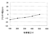
上述のエッチング装置を用いて、静電吸着電圧とプラズマ電位の相関について実験を行い調査した。本評価では、真空容器110内にHBrとO2ガスを導入し、高周波電源101のパワーを500W、試料台に印加する高周波電源115のパワーは35Wとした。このとき、プラズマ電位をDCプローブを用いて測定し、正の直流電源113Aにより内電極114Aに印加する電圧と、負の直流電源113Bにより外電極114Bに印加する電圧との関係を調査したところ、図5のように内電極114Aに印加する電圧が大きい場合と外電極114Bに印加する電圧の絶対値が小さい程、プラズマ電位が上昇することが判った。また、同時に真空容器内を覗き窓117より観察したところ、プラズマ電位が50V以上の領域で異常放電が発生しやすいことが判った。
Using the above-described etching apparatus, an experiment was conducted to investigate the correlation between the electrostatic adsorption voltage and the plasma potential. In this evaluation, HBr and O 2 gas were introduced into the
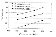
次に、試料台108に印加する高周波電源115のパワー(ピークトゥーピーク電圧)を可変し、高周波電源115のピークトゥーピーク電圧に対するプラズマ電位を測定した。測定の結果、図6に示すように、ピークトゥーピーク電圧が大きい程プラズマ電位が高くなる傾向があることが判った。図6から判るように、ピークトゥーピーク電圧の値により、プラズマ電位の上昇による異常放電を抑制するためすなわちプラズマ電位の上昇を抑制するための適正な吸着電圧値が異なる。実験から、基準の吸着電圧に対してピークトゥーピーク電圧値の約3分の1程度、吸着電圧値を負側にシフトさせれば、十分なマージンを確保しつつ、プラズマ電位が50Vをこえず、異常放電が発生しないことが判った。たとえば、基準の吸着電圧が内側:+500V、外側:−500Vでピークトゥーピーク電圧が600Vの場合、吸着電圧を200V負側にシフトさせて、内側:+300V、外側:−700Vとした。
Next, the power (peak to peak voltage) of the high
また、上記の装置において、ピークトゥーピーク電圧に対して正および負の吸着電圧を変更することの出来る制御回路を設け、異常放電抑制の実験を行った。本評価では、真空容器110内にHBrとO2ガスを導入し、高周波電源101のパワーを500W、試料台に印加する高周波電源115のパワーを増加し、ピークトゥーピーク電圧が、約500Vから1000Vの範囲で増加するようにして、異常放電の有無を覗き窓117より観察した。その結果、放電開始直後のピークトゥーピーク電圧値の4分の1から2分の1、静電吸着電圧をマイナス側にシフトさせることで上記ピークトゥーピーク電圧の範囲で異常放電の発生は観られなかった。
Further, in the above apparatus, a control circuit capable of changing the positive and negative adsorption voltages with respect to the peak-to-peak voltage was provided, and an experiment for suppressing abnormal discharge was performed. In this evaluation, HBr and O 2 gas are introduced into the
次に、本発明の第3の実施例を述べる。図7は、本発明の第3の実施例を適用するプラズマ処理装置のプラズマ生成部の詳細を示した図である。本実施例は、プラズマを生成する手段としては、図1あるいは図4に示したものと同一である。たとえば、φ200mmまたはφ300mmの試料107を載置する試料台108は、図1あるいは図4で述べたモノポール型あるいはダイポール型の電極を有している。
Next, a third embodiment of the present invention will be described. FIG. 7 is a diagram showing details of the plasma generation unit of the plasma processing apparatus to which the third embodiment of the present invention is applied. In the present embodiment, the means for generating plasma is the same as that shown in FIG. 1 or FIG. For example, the
第3の実施例では、真空容器(リアクタ)110内部に直流的に導通可能な導電性部材を配することを特徴とする。この導電性部材は、Cl2やHBr、CF4等の腐食性ガスプラズマ下で耐食性を有し、かつ重金属汚染を発生させない部材である必要がある。本実施例では、たとえばSiC焼結セラミックスをリング状に配した導電性部材1000をリアクタ下部に配している。
The third embodiment is characterized in that a conductive member capable of direct current conduction is disposed inside the vacuum vessel (reactor) 110. This conductive member needs to be a member that has corrosion resistance under corrosive gas plasma such as Cl 2 , HBr, and CF 4 and that does not cause heavy metal contamination. In this embodiment, for example, a
導電性部材1000の設置場所は、プラズマの密度の比較的高い場所である必要があり、極端なリアクタ下部のようなプラズマが届いていない場所は適切ではない。部材の面積は、プラズマ106からのリーク電流を処理するのに十分な面積が必要であり、実験的には50cm2以上必要である。導電性部材1000の抵抗率は、1KΩ以下であれば良く、良導体である必要は無い。
The installation place of the
図8に示すように、導電性部材1000をリアクタ内に導入した場合の実験を実施した。導電性部材を導入した場合、導入しない場合に比べて、静電吸着電圧をいかなる値で運転しても、異常放電を引き起こすプラズマ電位には至らないことがわかる。
As shown in FIG. 8, an experiment was conducted when the
尚、本実施例ではHBrとO2のガスによる誘導結合プラズマ処理装置を例にとって説明したが、本技術は、プラズマのガス種や放電方式を問わず、反応性イオンエッチング、マグネトロンエッチング、誘導結合型プラズマエッチング等の処理装置にも応用可能であることは言うまでもない。 In this embodiment, the inductively coupled plasma processing apparatus using HBr and O 2 gas has been described as an example. However, the present technology is applicable to reactive ion etching, magnetron etching, inductive coupling regardless of the plasma gas type and discharge method. Needless to say, the present invention can also be applied to a processing apparatus such as mold plasma etching.
101…高周波電源、102…マッチングボックス、103…アンテナ、104…誘導結合窓、106…プラズマ、107…試料、108…試料台、109…誘電膜、110…真空容器、111…円筒、112…アース電極、113…直流電源、113A…内側直流電源、113B…外側直流電源、114…電極、114A…内電極、114B…外電極、115…バイアス用高周波電源、116…熱媒体温度コントローラ、117…覗き窓、10000−導電性部材
DESCRIPTION OF
Claims (10)
前記真空処理室内のプラズマに曝される内壁表面を絶縁性部材で取り囲み、
前記プラズマのプラズマ電位の上昇を抑制するために、前記静電吸着電圧を前記高周波バイアス電力のピークトゥーピーク電圧(peak to peak)をモニタし、その4分の1から2分の1の電位分負側に移行させることを特徴とするプラズマ処理方法。 A first high-frequency source for generating plasma in a vacuum chamber; a sample stage provided with a dielectric film including an electrostatic adsorption electrode for electrostatically adsorbing the sample; and a high-frequency bias power applied to the sample on the sample stage In a plasma processing method of a plasma processing apparatus, comprising: a second high frequency source to be applied; and a direct current power source for applying an electrostatic adsorption voltage to the electrodes in the dielectric film.
Surrounding the inner wall surface exposed to the plasma in the vacuum processing chamber with an insulating member,
In order to suppress the increase of the plasma potential of the plasma, the electrostatic attraction voltage monitors the high frequency bias power peak-to-peak voltage (peak to peak), 1 potential from a quarter of the half of its A plasma processing method, wherein the plasma processing method is characterized in that it is shifted to the negative side.
前記静電吸着電圧の移行を、前記高周波バイアス電力のピークトゥーピーク電圧のモニタによる結果、またはあらかじめわかっているピークトゥーピーク電圧の予想値に応じた、移行電圧のレシピ設定により行うことを特徴するプラズマ処理方法。 The plasma processing method according to claim 1,
The transfer of the electrostatic adsorption voltage is performed by setting the transfer voltage according to the result of monitoring the peak-to-peak voltage of the high-frequency bias power or the predicted value of the known peak-to-peak voltage. Plasma processing method.
試料台に配置した静電吸着電極は、モノポール方式またはダイポール方式のいずれかであることを特徴とするプラズマ処理方法。 In the plasma processing method of Claim 1 or Claim 2,
The plasma processing method, wherein the electrostatic adsorption electrode arranged on the sample stage is either a monopole method or a dipole method.
試料台に配置した静電吸着電極は、静電吸着電極がダイポール方式であるときに、静電吸着電圧を双極ともにマイナス側に50〜500Vずらすことを特徴とするプラズマ処理方法。 The plasma processing method according to claim 3, wherein
The plasma processing method characterized in that the electrostatic chucking electrode arranged on the sample stage shifts the electrostatic chucking voltage to the negative side by 50 to 500 V in both bipolar directions when the electrostatic chucking electrode is a dipole system.
プラズマ処理装置内のプラズマを取り囲む面を絶縁性部材と一部導電性部材で取り囲んだことを特徴とするプラズマ処理方法。 The plasma processing method according to claim 1,
A plasma processing method characterized in that a surface surrounding plasma in a plasma processing apparatus is surrounded by an insulating member and a part of a conductive member.
前記真空処理室内のプラズマに曝される内壁表面を絶縁性部材で取り囲んで構成し、前記プラズマのプラズマ電位の上昇を抑制するために、前記静電吸着電圧を負側に変化させる制御手段を備え、
前記制御手段が、静電吸着電圧を前記高周波バイアス電力のピークトゥーピーク電圧をモニタし、その4分の1から2分の1の電位分負側に移行するよう制御する手段であることを特徴とするプラズマ処理装置。 A first high-frequency source for generating plasma in the vacuum processing chamber; a sample stage provided with a dielectric film including an electrostatic adsorption electrode for electrostatically adsorbing the sample; and a high-frequency bias power applied to the sample on the sample stage In a plasma processing apparatus comprising: a second high-frequency source for applying a voltage; and a DC power source for applying an electrostatic adsorption voltage to the electrodes in the dielectric film,
The inner surface of the vacuum processing chamber exposed to plasma is surrounded by an insulating member, and control means is provided for changing the electrostatic adsorption voltage to the negative side in order to suppress an increase in plasma potential of the plasma. ,
Said control means, the electrostatic attraction voltage monitors peak-to-peak voltage of the high frequency bias power, is a means for controlling so as to shift from one quarter of that in the first potential worth negative half A plasma processing apparatus.
前記制御手段が、前記静電吸着電圧の移行を、前記高周波バイアス電力のピークトゥーピーク電圧のモニタによる結果、またはあらかじめわかっているピークトゥーピーク電圧の予想値に応じた、移行電圧のレシピ設定により行う手段であることを特徴するプラズマ処理装置。 The plasma processing apparatus according to claim 6, wherein
The control means determines the transition of the electrostatic adsorption voltage by setting the transition voltage according to the result of monitoring the peak-to-peak voltage of the high-frequency bias power or the predicted value of the peak-to-peak voltage that is known in advance. A plasma processing apparatus characterized by being a means for performing.
Priority Applications (4)
| Application Number | Priority Date | Filing Date | Title |
|---|---|---|---|
| JP2005022112A JP4468194B2 (en) | 2005-01-28 | 2005-01-28 | Plasma processing method and plasma processing apparatus |
| TW094105872A TWI290345B (en) | 2005-01-28 | 2005-02-25 | Plasma processing method and plasma processing apparatus |
| KR1020050016720A KR100757528B1 (en) | 2005-01-28 | 2005-02-28 | Plasma processing method and plasma processing apparatus |
| US11/069,551 US7224568B2 (en) | 2005-01-28 | 2005-03-02 | Plasma processing method and plasma processing apparatus |
Applications Claiming Priority (1)
| Application Number | Priority Date | Filing Date | Title |
|---|---|---|---|
| JP2005022112A JP4468194B2 (en) | 2005-01-28 | 2005-01-28 | Plasma processing method and plasma processing apparatus |
Publications (3)
| Publication Number | Publication Date |
|---|---|
| JP2006210726A JP2006210726A (en) | 2006-08-10 |
| JP2006210726A5 JP2006210726A5 (en) | 2006-12-21 |
| JP4468194B2 true JP4468194B2 (en) | 2010-05-26 |
Family
ID=36756289
Family Applications (1)
| Application Number | Title | Priority Date | Filing Date |
|---|---|---|---|
| JP2005022112A Active JP4468194B2 (en) | 2005-01-28 | 2005-01-28 | Plasma processing method and plasma processing apparatus |
Country Status (4)
| Country | Link |
|---|---|
| US (1) | US7224568B2 (en) |
| JP (1) | JP4468194B2 (en) |
| KR (1) | KR100757528B1 (en) |
| TW (1) | TWI290345B (en) |
Families Citing this family (27)
| Publication number | Priority date | Publication date | Assignee | Title |
|---|---|---|---|---|
| JP5094002B2 (en) | 2005-09-06 | 2012-12-12 | ルネサスエレクトロニクス株式会社 | Plasma processing apparatus and method for suppressing abnormal discharge thereof |
| JP5372419B2 (en) * | 2008-06-25 | 2013-12-18 | 株式会社日立ハイテクノロジーズ | Plasma processing apparatus and plasma processing method |
| DE102008036766B4 (en) * | 2008-08-07 | 2013-08-01 | Alexander Gschwandtner | Apparatus and method for generating dielectric layers in microwave plasma |
| US9063356B2 (en) | 2008-09-05 | 2015-06-23 | Japan Display Inc. | Method for repairing display device and apparatus for same |
| US9767988B2 (en) | 2010-08-29 | 2017-09-19 | Advanced Energy Industries, Inc. | Method of controlling the switched mode ion energy distribution system |
| US11615941B2 (en) | 2009-05-01 | 2023-03-28 | Advanced Energy Industries, Inc. | System, method, and apparatus for controlling ion energy distribution in plasma processing systems |
| JP2011187881A (en) * | 2010-03-11 | 2011-09-22 | Hitachi High-Technologies Corp | Plasma processing device and method |
| US9685297B2 (en) | 2012-08-28 | 2017-06-20 | Advanced Energy Industries, Inc. | Systems and methods for monitoring faults, anomalies, and other characteristics of a switched mode ion energy distribution system |
| US9875881B2 (en) * | 2013-02-20 | 2018-01-23 | Tokyo Electron Limited | Plasma processing apparatus and plasma processing method |
| JP6357436B2 (en) | 2014-07-25 | 2018-07-11 | 株式会社日立ハイテクノロジーズ | Plasma processing equipment |
| KR101677748B1 (en) | 2014-10-29 | 2016-11-29 | 삼성전자 주식회사 | Pulse plasma apparatus and method for operating the same |
| US9779919B2 (en) | 2015-01-09 | 2017-10-03 | Hitachi High-Technologies Corporation | Plasma processing apparatus and plasma processing method |
| JP6567943B2 (en) | 2015-01-09 | 2019-08-28 | 株式会社日立ハイテクノロジーズ | Plasma processing apparatus and plasma processing method |
| JP6396822B2 (en) * | 2015-02-16 | 2018-09-26 | 東京エレクトロン株式会社 | Method for controlling potential of susceptor of plasma processing apparatus |
| US9824857B2 (en) * | 2016-01-14 | 2017-11-21 | Varian Semiconductor Equipment Associates, Inc. | Method for implantation of semiconductor wafers having high bulk resistivity |
| US10535505B2 (en) * | 2016-11-11 | 2020-01-14 | Lam Research Corporation | Plasma light up suppression |
| TW202329762A (en) | 2017-11-17 | 2023-07-16 | 新加坡商Aes 全球公司 | Systems and methods for spatially and temporally controlling plasma processing on substrates and related computer-readable medium |
| JP2021503702A (en) | 2017-11-17 | 2021-02-12 | エーイーエス グローバル ホールディングス, プライベート リミテッド | Improved application of modulation sources in plasma processing systems |
| PL3711080T3 (en) | 2017-11-17 | 2023-12-11 | Aes Global Holdings, Pte. Ltd. | Synchronized pulsing of plasma processing source and substrate bias |
| KR102524810B1 (en) | 2017-12-26 | 2023-04-24 | 삼성전자주식회사 | Method for controlling semiconductor process |
| TW202105591A (en) | 2019-04-15 | 2021-02-01 | 美商應用材料股份有限公司 | Electrostatic chucking process |
| JP2022541004A (en) | 2019-07-12 | 2022-09-21 | エーイーエス グローバル ホールディングス, プライベート リミテッド | Bias supply device with single controlled switch |
| KR102662551B1 (en) * | 2021-02-25 | 2024-05-03 | 주식회사 히타치하이테크 | plasma processing device |
| US12046448B2 (en) | 2022-01-26 | 2024-07-23 | Advanced Energy Industries, Inc. | Active switch on time control for bias supply |
| US11942309B2 (en) | 2022-01-26 | 2024-03-26 | Advanced Energy Industries, Inc. | Bias supply with resonant switching |
| US11670487B1 (en) | 2022-01-26 | 2023-06-06 | Advanced Energy Industries, Inc. | Bias supply control and data processing |
| US11978613B2 (en) | 2022-09-01 | 2024-05-07 | Advanced Energy Industries, Inc. | Transition control in a bias supply |
Family Cites Families (3)
| Publication number | Priority date | Publication date | Assignee | Title |
|---|---|---|---|---|
| US5557215A (en) | 1993-05-12 | 1996-09-17 | Tokyo Electron Limited | Self-bias measuring method, apparatus thereof and electrostatic chucking apparatus |
| US5737177A (en) * | 1996-10-17 | 1998-04-07 | Applied Materials, Inc. | Apparatus and method for actively controlling the DC potential of a cathode pedestal |
| US6367413B1 (en) * | 1999-06-15 | 2002-04-09 | Tokyo Electron Limited | Apparatus for monitoring substrate biasing during plasma processing of a substrate |
-
2005
- 2005-01-28 JP JP2005022112A patent/JP4468194B2/en active Active
- 2005-02-25 TW TW094105872A patent/TWI290345B/en active
- 2005-02-28 KR KR1020050016720A patent/KR100757528B1/en active IP Right Grant
- 2005-03-02 US US11/069,551 patent/US7224568B2/en active Active
Also Published As
| Publication number | Publication date |
|---|---|
| KR20060087358A (en) | 2006-08-02 |
| TWI290345B (en) | 2007-11-21 |
| TW200627540A (en) | 2006-08-01 |
| US7224568B2 (en) | 2007-05-29 |
| US20060171093A1 (en) | 2006-08-03 |
| KR100757528B1 (en) | 2007-09-11 |
| JP2006210726A (en) | 2006-08-10 |
Similar Documents
| Publication | Publication Date | Title |
|---|---|---|
| JP4468194B2 (en) | Plasma processing method and plasma processing apparatus | |
| JP5317424B2 (en) | Plasma processing equipment | |
| JP4838736B2 (en) | Plasma processing equipment | |
| JP4421874B2 (en) | Plasma processing apparatus and plasma processing method | |
| JP6173313B2 (en) | Electrostatic chuck with plasma-assisted dechuck on wafer backside | |
| JP5063520B2 (en) | Plasma processing method and plasma processing apparatus | |
| JP4704088B2 (en) | Plasma processing equipment | |
| TWI505354B (en) | Dry etching apparatus and dry etching method | |
| US20080236492A1 (en) | Plasma processing apparatus | |
| US7767055B2 (en) | Capacitive coupling plasma processing apparatus | |
| US20100078129A1 (en) | Mounting table for plasma processing apparatus | |
| US9011635B2 (en) | Plasma processing apparatus | |
| JP2000331993A (en) | Plasma processing device | |
| US20190006156A1 (en) | Plasma Processing Apparatus | |
| US20080242086A1 (en) | Plasma processing method and plasma processing apparatus | |
| US10847348B2 (en) | Plasma processing apparatus and plasma processing method | |
| KR20150055549A (en) | Substrate processing method and substrate processing device | |
| JP2006165093A (en) | Plasma processing device | |
| JP2010010214A (en) | Method for manufacturing semiconductor device, semiconductor manufacturing apparatus and storage medium | |
| US7601241B2 (en) | Plasma processing apparatus and plasma processing method | |
| US8034213B2 (en) | Plasma processing apparatus and plasma processing method | |
| JP2015072825A (en) | Plasma processing device and plasma processing method | |
| JP2011124295A (en) | Plasma processing apparatus | |
| JP5640135B2 (en) | Plasma processing equipment | |
| JP2011071211A (en) | Method of measuring self-bias of processing object, and method and device for separating processing object using the same |
Legal Events
| Date | Code | Title | Description |
|---|---|---|---|
| A521 | Request for written amendment filed |
Free format text: JAPANESE INTERMEDIATE CODE: A523 Effective date: 20061107 |
|
| A621 | Written request for application examination |
Free format text: JAPANESE INTERMEDIATE CODE: A621 Effective date: 20061107 |
|
| A977 | Report on retrieval |
Free format text: JAPANESE INTERMEDIATE CODE: A971007 Effective date: 20080926 |
|
| A131 | Notification of reasons for refusal |
Free format text: JAPANESE INTERMEDIATE CODE: A131 Effective date: 20081007 |
|
| A521 | Request for written amendment filed |
Free format text: JAPANESE INTERMEDIATE CODE: A523 Effective date: 20081208 |
|
| A131 | Notification of reasons for refusal |
Free format text: JAPANESE INTERMEDIATE CODE: A131 Effective date: 20090908 |
|
| A521 | Request for written amendment filed |
Free format text: JAPANESE INTERMEDIATE CODE: A523 Effective date: 20091105 |
|
| A131 | Notification of reasons for refusal |
Free format text: JAPANESE INTERMEDIATE CODE: A131 Effective date: 20091201 |
|
| A521 | Request for written amendment filed |
Free format text: JAPANESE INTERMEDIATE CODE: A523 Effective date: 20100128 |
|
| TRDD | Decision of grant or rejection written | ||
| A01 | Written decision to grant a patent or to grant a registration (utility model) |
Free format text: JAPANESE INTERMEDIATE CODE: A01 Effective date: 20100223 |
|
| A01 | Written decision to grant a patent or to grant a registration (utility model) |
Free format text: JAPANESE INTERMEDIATE CODE: A01 |
|
| A61 | First payment of annual fees (during grant procedure) |
Free format text: JAPANESE INTERMEDIATE CODE: A61 Effective date: 20100224 |
|
| R150 | Certificate of patent or registration of utility model |
Ref document number: 4468194 Country of ref document: JP Free format text: JAPANESE INTERMEDIATE CODE: R150 Free format text: JAPANESE INTERMEDIATE CODE: R150 |
|
| FPAY | Renewal fee payment (event date is renewal date of database) |
Free format text: PAYMENT UNTIL: 20130305 Year of fee payment: 3 |
|
| FPAY | Renewal fee payment (event date is renewal date of database) |
Free format text: PAYMENT UNTIL: 20130305 Year of fee payment: 3 |
|
| S531 | Written request for registration of change of domicile |
Free format text: JAPANESE INTERMEDIATE CODE: R313531 |
|
| S533 | Written request for registration of change of name |
Free format text: JAPANESE INTERMEDIATE CODE: R313533 |
|
| R350 | Written notification of registration of transfer |
Free format text: JAPANESE INTERMEDIATE CODE: R350 |