JP2007208302A - Plasma processing method and plasma processing device - Google Patents
Plasma processing method and plasma processing device Download PDFInfo
- Publication number
- JP2007208302A JP2007208302A JP2007128741A JP2007128741A JP2007208302A JP 2007208302 A JP2007208302 A JP 2007208302A JP 2007128741 A JP2007128741 A JP 2007128741A JP 2007128741 A JP2007128741 A JP 2007128741A JP 2007208302 A JP2007208302 A JP 2007208302A
- Authority
- JP
- Japan
- Prior art keywords
- plasma
- frequency power
- applying
- plasma processing
- substrate
- Prior art date
- Legal status (The legal status is an assumption and is not a legal conclusion. Google has not performed a legal analysis and makes no representation as to the accuracy of the status listed.)
- Granted
Links
Images


Landscapes
- Drying Of Semiconductors (AREA)
Abstract
Description
本発明は、プラズマ処理方法及びプラズマ処理装置に係り、特に半導体ウエハやLCD用基板等の被処理基板にプラズマエッチング処理等を施すプラズマ処理方法及びプラズマ処理装置に関する。 The present invention relates to a plasma processing method and a plasma processing apparatus, and more particularly to a plasma processing method and a plasma processing apparatus for performing a plasma etching process or the like on a target substrate such as a semiconductor wafer or an LCD substrate.
従来から、プラズマによって、半導体ウエハやLCD用基板等の被処理基板の処理を行うプラズマ処理方法が多用されている。例えば、半導体装置の製造工程においては、被処理基板、例えば半導体ウエハに、微細な電気回路を形成するための技術として、半導体ウエハ上に形成された薄膜等を、プラズマを用いてエッチングして除去するプラズマエッチング処理が多用されている。 2. Description of the Related Art Conventionally, a plasma processing method for processing a substrate to be processed such as a semiconductor wafer or an LCD substrate with plasma has been widely used. For example, in a manufacturing process of a semiconductor device, as a technique for forming a fine electric circuit on a substrate to be processed, for example, a semiconductor wafer, a thin film formed on the semiconductor wafer is removed by etching using plasma. A plasma etching process is frequently used.
かかるプラズマエッチング処理を行うエッチング装置では、例えば、内部を気密に閉塞可能に構成された処理チャンバー(エッチングチャンバー)内でプラズマを発生させるようになっている。そして、このエッチングチャンバー内に設けたサセプタ上に半導体ウエハを載置して、エッチングを行う。 In an etching apparatus that performs such plasma etching processing, for example, plasma is generated in a processing chamber (etching chamber) configured to be hermetically closed. Then, the semiconductor wafer is placed on a susceptor provided in the etching chamber and etching is performed.
また、上記プラズマを発生させる手段については、種々のタイプが知られている。そのうち、上下に対向するように設けられた一対の平行平板電極に高周波電力を供給してプラズマを発生させるタイプの装置では、平行平板電極のうちの一方、例えば、下部電極がサセプタを兼ねている。そして、この下部電極上に半導体ウエハを配置し、平行平板電極間に高周波電圧を印加してプラズマを発生させ、エッチングを行う。 Various types of means for generating the plasma are known. Among them, in a type of apparatus that generates plasma by supplying high-frequency power to a pair of parallel plate electrodes provided so as to face each other vertically, one of the parallel plate electrodes, for example, the lower electrode also serves as a susceptor. . Then, a semiconductor wafer is disposed on the lower electrode, a high frequency voltage is applied between the parallel plate electrodes, plasma is generated, and etching is performed.
しかしながら、このようなエッチング装置では、エッチング中に、半導体ウエハの表面で、雷状の異常放電が生じる所謂表面アーキングが生じることがある。 However, in such an etching apparatus, so-called surface arcing that causes lightning-like abnormal discharge may occur on the surface of the semiconductor wafer during etching.
上記表面アーキングは、例えば、導体層の上に絶縁体層が形成され、かかる絶縁体層をエッチングするような場合、例えば、シリコン酸化膜からなる絶縁体層をエッチングして、下層のメタル層からなる導体層に通じるコンタクトホールを形成する場合等に、エッチングによって膜厚が減少したシリコン酸化膜を破壊するように生じる場合が多い。 For example, when the insulator layer is formed on the conductor layer and the insulator layer is etched, the surface arcing is performed by etching the insulator layer made of a silicon oxide film, for example, from the lower metal layer. In many cases, such as when a contact hole leading to a conductive layer is formed, the silicon oxide film whose thickness is reduced by etching is destroyed.
そして、かかる異常放電が生じると、半導体ウエハ中のシリコン酸化膜の多くの部分が破壊されてしまうため、その半導体ウエハの大部分の素子が不良となってしまう。また、これとともに、エッチングチャンバー内に金属汚染が生じ、そのまま続けてエッチング処理を行うことができず、エッチングチャンバー内のクリーニングが必要となる。このため、生産性が著しく低下してしまうという問題があった。 When such an abnormal discharge occurs, many parts of the silicon oxide film in the semiconductor wafer are destroyed, so that most elements of the semiconductor wafer become defective. At the same time, metal contamination occurs in the etching chamber, so that the etching process cannot be performed continuously, and the etching chamber needs to be cleaned. For this reason, there has been a problem in that productivity is significantly reduced.
本発明は、かかる従来の事情に対処してなされたもので、被処理基板に生じる表面アーキングの発生を防止して、従来に較べて生産性の向上を図ることのできるプラズマ処理方法及びプラズマ処理装置を提供しようとするものである。 The present invention has been made in response to such a conventional situation, and a plasma processing method and a plasma processing which can prevent the occurrence of surface arcing occurring in a substrate to be processed and can improve the productivity as compared with the prior art. The device is to be provided.
請求項1の発明は、被処理基板にプラズマを作用させてプラズマ処理を行うプラズマ処理方法であって、当該プラズマ処理を行う処理チャンバー内に前記被処理基板を搬入した後で且つ前記プラズマ処理を行う前に、前記被処理基板を載置する下部電極に低いパワーの高周波電力を印加する工程と、前記下部電極に対向して設けられた上部電極に低いパワーの高周波電力を印加する工程と、前記被処理基板を吸着保持するための静電チャックに直流電圧を印加する工程と、前記下部電極に高いパワーの高周波電力を印加する工程と、
前記上部電極に高いパワーの高周波電力を印加して、前記被処理基板にプラズマ処理を行う工程と、を上記の順で有することを特徴とする。
The invention of
And a step of applying plasma processing to the substrate to be processed by applying high-frequency high-frequency power to the upper electrode in the order described above.
請求項2の発明は、請求項1記載のプラズマ処理方法であって、前記上部電極に低いパワーの高周波電力を印加する工程と、前記静電チャックに直流電圧を印加する工程との間に、前記下部電極への低いパワーの高周波電力の印加を停止する工程と、前記上部電極への低いパワーの高周波電力の印加を停止する工程と、を有することを特徴とする。
Invention of
請求項3の発明は、請求項1又は2記載のプラズマ処理方法であって、前記上部電極に低いパワーの高周波電力を印加する工程において、前記プラズマ処理に使用するプラズマよりも弱いプラズマが前記被処理基板に作用され、前記弱いプラズマが、Arガス、又はO2 ガス、又はCF4 ガス、又はN2 ガスによって形成されたプラズマであることを特徴とする。 A third aspect of the present invention is the plasma processing method according to the first or second aspect, wherein in the step of applying high-frequency power of low power to the upper electrode, a plasma weaker than the plasma used for the plasma processing is applied. The weak plasma is a plasma formed by Ar gas, O 2 gas, CF 4 gas, or N 2 gas.
請求項4の発明は、請求項1〜3いずれか1項記載のプラズマ処理方法であって、前記上部電極に低いパワーの高周波電力を印加する工程において、前記プラズマ処理に使用するプラズマよりも弱いプラズマが前記被処理基板に作用され、前記弱いプラズマが、0.15〜1.0W/cm2の高周波電力によって形成されることを特徴とする。
Invention of
請求項5の発明は、請求項1〜4いずれか1項記載のプラズマ処理方法であって、前記上部電極に低いパワーの高周波電力を印加する工程において、前記プラズマ処理に使用するプラズマよりも弱いプラズマが前記被処理基板に作用され、前記弱いプラズマを、5〜20秒の間前記被処理基板に作用させることを特徴とする。
Invention of
請求項6の発明は、真空排気可能な処理チャンバーを有し、前記処理チャンバー内で被処理基板にプラズマ処理を行うプラズマ処理装置であって、前記処理チャンバー内に配置された、前記被処理基板を載置する下部電極と、前記下部電極に対向して設けられた上部電極と、前記下部電極に高周波電力を印加するための第1の高周波電源と、前記上部電極に高周波電力を印加するための第2の高周波電源と、前記被処理基板を吸着保持するための静電チャックと、前記静電チャックに直流電圧を供給する直流電源と、プラズマを生成させるためのガスを供給するガス供給系と、前記第1の高周波電源と前記第2の高周波電源と前記直流電源と前記ガス供給系とを制御する制御部とを具備し、前記制御部は、前記処理チャンバー内に前記被処理基板を搬入した後で且つ前記プラズマ処理を行う前に、前記下部電極に前記第1の高周波電源からの低いパワーの高周波電力を印加する工程と、前記上部電極に前記第2の高周波電源からの低いパワーの高周波電力を印加する工程と、前記静電チャックに前記直流電源からの直流電圧を印加する工程と、前記下部電極に前記第1の高周波電源からの高いパワーの高周波電力を印加する工程と、前記上部電極に前記第2の高周波電源からの高いパワーの高周波電力を印加して、前記被処理基板にプラズマ処理を行う工程と、が上記の順で行われるように制御することを特徴する。
The invention of
請求項7の発明は、請求項6記載のプラズマ処理装置であって、前記制御部は、前記上部電極に低いパワーの高周波電力を印加する工程と、前記静電チャックに直流電圧を印加する工程との間に、前記下部電極への低いパワーの高周波電力の印加を停止する工程と、前記上部電極への低いパワーの高周波電力の印加を停止する工程と、が行われるように制御することを特徴とする。 A seventh aspect of the present invention is the plasma processing apparatus according to the sixth aspect, wherein the control unit applies a low-frequency high-frequency power to the upper electrode and applies a DC voltage to the electrostatic chuck. Between the step of stopping the application of the low-power high-frequency power to the lower electrode and the step of stopping the application of the low-power high-frequency power to the upper electrode. Features.
請求項8の発明は、請求項6又は7記載のプラズマ処理装置であって、前記制御部は、前記上部電極に低いパワーの高周波電力を印加する工程において、前記プラズマ処理に使用するプラズマよりも弱いプラズマが前記被処理基板に作用するように制御し、前記弱いプラズマが、Arガス、又はO2 ガス、又はCF4 ガス、又はN2 ガスによって形成されたプラズマであることを特徴とする。
Invention of
請求項9の発明は、請求項6〜8いずれか1項記載のプラズマ処理装置であって、前記制御部は、前記上部電極に低いパワーの高周波電力を印加する工程において、前記プラズマ処理に使用するプラズマよりも弱いプラズマが前記被処理基板に作用するように制御し、前記弱いプラズマが、0.15〜1.0W/cm2の高周波電力によって形成されることを特徴とする。 A ninth aspect of the present invention is the plasma processing apparatus according to any one of the sixth to eighth aspects, wherein the control unit is used for the plasma processing in a step of applying high-frequency power of low power to the upper electrode. Control is performed so that a plasma weaker than the plasma to be applied acts on the substrate to be processed, and the weak plasma is formed by a high frequency power of 0.15 to 1.0 W / cm 2 .
請求項10の発明は、請求項6〜9いずれか1項記載のプラズマ処理装置であって、前記制御部は、前記上部電極に低いパワーの高周波電力を印加する工程において、前記プラズマ処理に使用するプラズマよりも弱いプラズマが前記被処理基板に作用するように制御し、前記弱いプラズマを、5〜20秒の間前記被処理基板に作用させることを特徴とする。 A tenth aspect of the present invention is the plasma processing apparatus according to any one of the sixth to ninth aspects, wherein the control unit is used for the plasma processing in a step of applying high-frequency power of low power to the upper electrode. Control is performed so that a plasma weaker than the plasma to be applied acts on the substrate to be processed, and the weak plasma is applied to the substrate to be processed for 5 to 20 seconds.
本発明によれば、被処理基板に生じる表面アーキングの発生を防止して、従来に較べて生産性の向上を図ることができる。 According to the present invention, it is possible to prevent the occurrence of surface arcing that occurs in the substrate to be processed, and to improve the productivity as compared with the prior art.
以下、本発明の詳細を、図面を参照して実施の形態について説明する。 The details of the present invention will be described below with reference to the drawings.
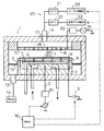
図1は、本発明の実施の形態に使用するプラズマ処理装置(エッチング装置)全体の概略構成を模式的に示すもので、同図において、符号1は、材質が例えばアルミニウム等からなり、内部を気密に閉塞可能に構成され、処理チャンバーを構成する円筒状の真空チャンバーを示している。
FIG. 1 schematically shows a schematic configuration of an entire plasma processing apparatus (etching apparatus) used in an embodiment of the present invention. In FIG. 1,
上記真空チャンバー1は、接地電位に接続されており、真空チャンバー1の内部には、導電性材料、例えばアルミニウム等からブロック状に構成され、下部電極を兼ねた載置台2が設けられている。
The
この載置台2は、セラミックなどの絶縁板3を介して真空チャンバー1内に支持されており、載置台2の半導体ウエハW載置面には、静電チャック4が設けられている。この静電チャック4は、静電チャック用電極4aを、絶縁性材料からなる絶縁膜4b中に介在させた構成とされており、静電チャック用電極4aには直流電源5が接続されている。静電チャック用電極4aは、例えば銅等から構成されており、絶縁膜4bはポリイミド等から構成されている。
The mounting table 2 is supported in the
また、載置台2の内部には、温度制御のための熱媒体としての絶縁性流体を循環させるための熱媒体流路6と、ヘリウムガス等の温度制御用のガスを半導体ウエハWの裏面に供給するためのガス流路7が設けられている。
Further, in the mounting table 2, a heat
そして、熱媒体流路6内に所定温度に制御された絶縁性流体を循環させることによって、載置台2を所定温度に制御し、かつ、この載置台2と半導体ウエハWの裏面との間にガス流路7を介して温度制御用のガスを供給してこれらの間の熱交換を促進し、半導体ウエハWを精度良くかつ効率的に所定温度に制御することができるようになっている。
Then, by circulating an insulating fluid controlled to a predetermined temperature in the heat
また、載置台2の上方の外周には導電性材料または絶縁性材料で形成されたフォーカスリング8が設けられており、さらに、載置台2のほぼ中央には、高周波電力を供給するための給電線9が接続されている。この給電線9には整合器10を介して、高周波電源(RF電源)11が接続され、高周波電源11からは、所定の周波数の高周波電力が供給されるようになっている。
In addition, a
また、上述したフォーカスリング8の外側には、環状に構成され、多数の排気孔が形成された排気リング12が設けられており、この排気リング12を介して、排気ポート13に接続された排気系14の真空ポンプ等により、真空チャンバー1内の処理空間の真空排気が行われるよう構成されている。
In addition, an
一方、載置台2の上方の真空チャンバー1の天壁部分には、シャワーヘッド15が、載置台2と平行に対向する如く設けられており、このシャワーヘッド15は接地されている。したがって、これらのシャワーヘッド15と載置台2は、一対の電極(上部電極と下部電極)として機能するようになっている。
On the other hand, a
上記シャワーヘッド15は、その下面に多数のガス吐出孔16が設けられており、且つその上部にガス導入部17を有している。そして、その内部にはガス拡散用空隙18が形成されている。ガス導入部17にはガス供給配管19が接続されており、このガス供給配管19の他端には、ガス供給系20が接続されている。このガス供給系20は、ガス流量を制御するためのマスフローコントローラ(MFC)21と、例えばエッチング用の処理ガス等を供給するための処理ガス供給源22、及び、Arガスを供給するためのArガス供給源23等から構成されている。
The
一方、真空チャンバー1の外側周囲には、真空チャンバー1と同心状に、環状の磁場形成機構(リング磁石)24が配置されており、載置台2とシャワーヘッド15との間の処理空間に磁場を形成するようになっている。この磁場形成機構24は、回転機構25によって、その全体が、真空チャンバー1の回りを所定の回転速度で回転可能とされている。
On the other hand, an annular magnetic field forming mechanism (ring magnet) 24 is arranged around the outside of the
また、半導体ウエハWにプラズマ処理を施すための上記直流電源5、高周波電源11、ガス供給系20等のプラズマ処理機構は、制御部40によって制御されるよう構成されている。
The plasma processing mechanisms such as the
次に、上記のように構成されたエッチング装置によるエッチング処理の手順について説明する。 Next, an etching process procedure performed by the etching apparatus configured as described above will be described.
(第1実施例) (First embodiment)
まず、真空チャンバー1に設けられた図示しないゲートバルブを開放し、このゲートバルブに隣接して配置されたロードロック室(図示せず)を介して、搬送機構(図示せず)により半導体ウエハWを真空チャンバー1内に搬入し、載置台2上に載置する。そして、搬送機構を真空チャンバー1外へ退避させた後、ゲートバルブを閉じる。なお、この時点では、静電チャック4の静電チャック用電極4aへの直流電源5からの直流電圧(HV)の印加は、行っていない。
First, a gate valve (not shown) provided in the
この後、排気系14の真空ポンプにより排気ポート13を通じて真空チャンバー1内を所定の真空度に排気しつつ、まず、Arガス供給源23から、真空チャンバー1内にArガスを供給し、この状態で、図2に示すように、まず高周波電源11から下部電極としての載置台2に、例えば、300W等の比較的パワーの低い高周波電力(周波数例えば13.56MHz)を供給して、弱いプラズマを発生させ、この弱いプラズマを半導体ウエハWに作用させる。
Thereafter, while exhausting the inside of the
このように、弱いプラズマを半導体ウエハWに作用させるのは、以下のような理由による。 The reason why the weak plasma acts on the semiconductor wafer W in this way is as follows.
すなわち、処理を行う半導体ウエハWは、前工程(例えばCVD等の成膜工程)における処理の状態等によって、その状態が一様でなく、例えば、半導体ウエハWの内部に電荷が蓄積されている場合がある。そして、このように半導体ウエハWの内部に電荷が蓄積された状態で、強いプラズマを作用させると、表面アーキング等を生じさせる可能性が高いため、かかる強いプラズマを作用させる前に、弱いプラズマを作用させて、半導体ウエハWの内部に蓄積された電荷の状態等を一様に調整する(初期化する)ためである。 That is, the state of the semiconductor wafer W to be processed is not uniform depending on the processing state in the previous step (for example, a film forming step such as CVD), and for example, charges are accumulated inside the semiconductor wafer W. There is a case. In addition, when strong plasma is applied in a state where charges are accumulated inside the semiconductor wafer W in this way, there is a high possibility that surface arcing or the like will occur. Therefore, before applying such strong plasma, weak plasma is applied. This is for the purpose of uniformly adjusting (initializing) the state of charges accumulated in the semiconductor wafer W by the action.
そして、このような半導体ウエハWの内部に蓄積された電荷の状態を調整するに当たり、半導体ウエハWの内部から電荷が移動し易くするために、静電チャック4の静電チャック用電極4aへの直流電圧(HV)の印加を行わない状態で、かかる弱いプラズマにより半導体ウエハの調整(初期化)を行う。
In adjusting the state of the charge accumulated inside the semiconductor wafer W, in order to facilitate the movement of the charge from the inside of the semiconductor wafer W, the
なお、このような弱いプラズマを発生させるための高周波印加電力は、0.15W/cm2〜1.0W/cm2程度、例えば、100〜500W程度であり、弱いプラズマを半導体ウエハWに作用させる時間は、例えば、5〜20秒程度である。 The high frequency applied power for generating such weak plasma is about 0.15 W / cm 2 to 1.0 W / cm 2 , for example, about 100 to 500 W, and the weak plasma is applied to the semiconductor wafer W. The time is, for example, about 5 to 20 seconds.
また、上記では、Arガスを用い、Arガスのプラズマを作用させる場合について説明しているが、ガス種はこれに限るものではなく、例えば、O2 ガス、CF4 ガス、N2 ガス等のガスも使用することができる。但し、このガス種の選択に当たっては、発生させるガスのプラズマが、半導体ウエハWに対して、及び、真空チャンバー1の内壁に対して、エッチング等の不所望な作用を起こす程度の少ないものを選択する必要があり、かつ、プラズマが着火し易いものを選択する必要がある。さらに、処理を行う半導体ウエハWが、前工程でどのような処理を施されたものであるかによっても、最適なガス種が変わる場合があり、これらを考慮して適宜選択することが好ましい。
In the above description, Ar gas is used and Ar gas plasma is applied. However, the gas type is not limited to this, and examples thereof include O 2 gas, CF 4 gas, and N 2 gas. Gas can also be used. However, in selecting this gas type, a gas gas with a low degree of undesired effects such as etching on the semiconductor wafer W and the inner wall of the
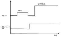
そして、上記のようにして半導体ウエハWに弱いプラズマを作用させた後、図2に示すように、静電チャック用電極4aへの直流電源5からの直流電圧(HV)の印加を行い、この後、処理ガス供給源22から真空チャンバー1内に所定の処理ガス(エッチングガス)を供給し、高周波電源11から下部電極としての載置台2に、例えば、2000W等の通常の処理用のパワーの高い高周波電力(周波数例えば13.56MHz)を供給して、強いプラズマを発生させ、通常のプラズマ処理(エッチング処理)を行う。なお、図2において、横軸は時間を表し、縦軸は静電チャックHVの場合には電圧値、RF出力の場合には電力値を表す。
Then, after applying a weak plasma to the semiconductor wafer W as described above, a DC voltage (HV) is applied from the
この時、下部電極である載置台2に高周波電力が印加されることにより、上部電極であるシャワーヘッド15と下部電極である載置台2との間の処理空間には高周波電界が形成されるとともに、磁場形成機構24による磁場が形成され、この状態でプラズマによるエッチングが行われる。
At this time, a high frequency electric field is formed in the processing space between the
そして、所定のエッチング処理が実行されると、高周波電源11からの高周波電力の供給を停止することによって、エッチング処理を停止し、上述した手順とは逆の手順で、半導体ウエハWを真空チャンバー1外に搬出する。
Then, when a predetermined etching process is executed, the etching process is stopped by stopping the supply of high-frequency power from the high-
上記のようにして、まず、半導体ウエハWに弱いプラズマを作用させ、この後、半導体ウエハWのエッチング処理を行ったところ、半導体ウエハWに表面アーキングが生じる割合を、ロットによらず、略ゼロ(1%以下)とすることができた。一方、上記のような弱いプラズマを作用させずに処理を開始した場合は、半導体ウエハWに表面アーキングが生じる割合がロットによっては、80%程度となる場合があった。エッチングより前の工程において、半導体ウエハWが帯電してしまったことが原因であり、このような表面アーキングは、前工程が、CVDによって所謂Low−K膜を形成する工程の場合に、特に発生する確率が高かった。 As described above, first, a weak plasma is applied to the semiconductor wafer W, and then the semiconductor wafer W is etched. As a result, the rate at which surface arcing occurs in the semiconductor wafer W is substantially zero regardless of the lot. (1% or less). On the other hand, when the processing is started without applying the weak plasma as described above, the ratio of occurrence of surface arcing on the semiconductor wafer W may be about 80% depending on the lot. This is because the semiconductor wafer W has been charged in the process prior to the etching, and such surface arcing occurs particularly when the so-called low-K film is formed by CVD. The probability of doing was high.
したがって、通常の処理を開始する前に、上記のように半導体ウエハWに弱いプラズマを作用させることによって、半導体ウエハWに表面アーキングが生じる割合を大幅に低下できることが確認できた。 Therefore, it was confirmed that by causing weak plasma to act on the semiconductor wafer W as described above before starting normal processing, the rate at which surface arcing occurs in the semiconductor wafer W can be significantly reduced.
ところで、上記の実施形態では、図1に示すように、下部電極である載置台2にのみ高周波電力が印加される構成の装置を使用した場合について説明したが、例えば、図3に示すように、上部電極としてのシャワーヘッド15にも、整合装置30を介して高周波電源31から高周波電力を印加するように構成された所謂上下部印加型のプラズマ処理装置についても、適用することができる。
In the above embodiment, as shown in FIG. 1, a case has been described in which an apparatus having a configuration in which high-frequency power is applied only to the mounting table 2 that is the lower electrode, but for example, as shown in FIG. 3. The so-called upper / lower application type plasma processing apparatus configured to apply the high frequency power from the high
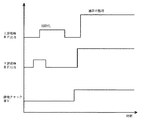
この場合、例えば、図4に示すように、まず、下部電極である載置台2に、低いパワーの高周波電力の印加を開始し、その後に上部電極であるシャワーヘッド15に低いパワーの高周波電力の印加を開始し、ここで一旦下部電極である載置台2に対する高周波電力の印加を停止する。そして、この状態で所定期間半導体ウエハWに弱いプラズマを作用させた後、上部電極であるシャワーヘッド15に対する高周波電力の印加も停止して、一旦プラズマを消す。
In this case, for example, as shown in FIG. 4, first, application of low-power high-frequency power to the mounting table 2 that is the lower electrode is started, and then low-frequency high-frequency power is applied to the
しかる後、静電チャック4の静電チャック用電極4aへの直流電圧(HV)の印加、下部電極である載置台2に対する処理用の通常の高周波電力(高パワーの高周波電力)の印加、上部電極であるシャワーヘッド15に対する処理用の通常の高周波電力(高パワーの高周波電力)の印加を、この順で開始し、半導体ウエハWの通常の処理を開始する。
Thereafter, application of DC voltage (HV) to the
このようにして、上下部印加型のプラズマ処理装置についても、本発明は適用することができる。 Thus, the present invention can also be applied to the upper and lower application type plasma processing apparatus.
なお、上記のように弱いプラズマを作用させるのに加えて、または、単独で、処理を開始する前に、半導体ウエハWに例えば、イオナイザーを作用させて、その内部の電荷を低減させることも好ましい。このようなイオナイザーの作用によって、表面アーキングの発生を抑制することもできる。このイオナイザーは、チャンバー内に設置してもよく、あるいはチャンバー外の別の場所に設置してもよい。 In addition to applying weak plasma as described above, or before starting the processing alone, it is also preferable to reduce the charge inside the semiconductor wafer W by applying, for example, an ionizer. . Generation of surface arcing can also be suppressed by the action of such an ionizer. The ionizer may be installed in the chamber or may be installed in another place outside the chamber.
ところで、図2に示したプラズマ処理方法では、下部電極である載置台2に弱い高周波電力を印加して弱いプラズマをたてた後の高周波電力が印加されていない状態で、静電チャック4の静電チャック用電極4aへの直流電圧(HV)の印加を開始している。このように、弱い高周波電力を印加して弱いプラズマをたてた後の高周波電力が印加されていない状態で、チャック用電極4aへの直流電圧(HV)の印加を開始すると、この直流電圧(HV)の印加を開始した際に、雷状の放電を発生させ基板に損傷を与える可能性がある。このような場合は、図5に示すように、載置台2に高周波電力が印加されている状態(弱いプラズマが生起されている状態)で、静電チャック用電極4aへの直流電圧(HV)の印加を開始すれば、放電の発生を、抑制することができる。
By the way, in the plasma processing method shown in FIG. 2, the
以上、第1実施例において、エッチング等のプラズマ処理前にArガスを用いて弱いプラズマをたてる方法、及びその際の静電チャック用電極4aへの直流電圧印加のタイミングについて説明した。
In the first embodiment, the method of generating weak plasma using Ar gas before plasma processing such as etching and the timing of applying DC voltage to the
(第2実施例) (Second embodiment)
次にエッチング処理等のプラズマ処理を行う際の高周波電力印加のタイミング及び静電チャック用電極4aへの直流電圧印加のタイミングとの関係について、好適な例を説明する。
Next, a preferred example will be described regarding the relationship between the timing of applying high-frequency power when performing plasma processing such as etching processing and the timing of applying DC voltage to the
なお、上記の静電チャック4には、双極型と単極型があり、また、これらのタイプに夫々クーロン型とジョンソンラーベック型とがある。このうち、単極型でクーロン型の静電チャック4を使用した場合、次のようなシーケンスで半導体ウエハWの吸着を行うことが好ましい。図6にそのシーケンスを表す。横軸は時間、縦軸は点線については印加高周波電力値(W)、実線については印加直流電圧値(V)を表している。
The
すなわち、半導体ウエハWを載置台2(静電チャック4)上に載置した後、真空チャンバー1内にガスの導入を開始する。そして、この後、図6に点線で示すように、まず、載置台2に高周波電力の印加を開始してプラズマを発生させ、この後、同図に実線で示すように、静電チャック用電極4aへの直流電圧(HV)の印加を行う。
That is, after the semiconductor wafer W is mounted on the mounting table 2 (electrostatic chuck 4), introduction of gas into the
なお、静電チャック用電極4aへの直流電圧(HV)の印加開始前は、半導体ウエハWが静電チャック4に吸着されていないため、その温度制御が充分に行われてはいない。このため、最初にプラズマを発生させる際に載置台2に印加する高周波電力は、処理を行う時に比べて低いパワーの高周波電力(例えば500W程度)とし、プラズマの作用によって、半導体ウエハWの温度が上昇しないようにすることが好ましい。
Note that the temperature of the semiconductor wafer W is not sufficiently controlled before the application of the DC voltage (HV) to the
そして、半導体ウエハWを静電チャック4から取り外す際も、同図に示すように、プラズマ処理が終了した後、まず、印加高周波電力値を、処理を行う時に比べて低いパワーの電力値(0Wではない)に下げる。この後、静電チャック用電極4aへの直流電圧(HV)の印加を停止し、しかる後、高周波電力の印加を停止してプラズマを消す。なお、静電チャック用電極4aへの直流電圧(HV)の印加を停止する際に、一旦吸着時とは逆極性の電圧(例えば−2000V程度)を静電チャック用電極4aへ印加して、電荷を除去し、半導体ウエハWを外し易くする。このような逆極性の電圧の印加は、必要に応じて行われ、かかる逆極性の電圧の印加を行わなくとも半導体ウエハWを静電チャック4から簡単に取り外すことができる場合は、逆極性の電圧の印加は行わない。
When removing the semiconductor wafer W from the
図7は、上記のような静電チャック4による半導体ウエハWの吸着のシーケンスの際の、静電チャック(ESC)の銅製の電極部(Cu)及びポリイミド製の絶縁膜部(PI)と、多層半導体ウエハ(Multi Layer Wafer )の裏面酸化膜部(B.S.Ox)及びシリコン基板部(Si sub )及び酸化膜部(Ox)と、真空チャンバー内の処理空間部(Space )及び上部電極部(Wall)の各部の電位の変化を示すものである。
FIG. 7 illustrates a copper electrode portion (Cu) and a polyimide insulating film portion (PI) of the electrostatic chuck (ESC) in the sequence of the adsorption of the semiconductor wafer W by the
同図に示すように、まず、載置台2に設けられたウエハ支持用のピンを降下させて半導体ウエハWを載置台2上に載置すると、図中(1)で示すように、各部の電位はゼロの状態であり、この後、真空チャンバー1内にガスの導入を開始した際も図中(2)で示すように、各部の電位はゼロの状態である。
As shown in the figure, first, when the wafer support pins provided on the mounting table 2 are lowered and the semiconductor wafer W is mounted on the mounting table 2, as shown by (1) in FIG. The potential is zero, and thereafter, when the introduction of gas into the
この後、高周波電力の印加を開始してプラズマを発生させると、図中(3)で示すように、半導体ウエハWの電位が、プラズマの状態で決まるマイナス数100V程度の電位となる。 Thereafter, when application of high-frequency power is started to generate plasma, as shown by (3) in the figure, the potential of the semiconductor wafer W becomes a potential of about minus several hundred volts determined by the plasma state.
そして、この状態で、静電チャック用電極4aへの直流電圧(HV)の印加を開始すると、図中(4)で示すように、静電チャック用電極4aの電位が、印加した直流電圧(HV)の電位(例えば、1.5KV程度)となり、絶縁膜部(PI)に電位差が生じて半導体ウエハWの吸着が行われる。
In this state, when application of the DC voltage (HV) to the
このように、上記のような静電チャック4による半導体ウエハWの吸着のシーケンスによれば、半導体ウエハWの表面に、静電チャック用電極4aへの直流電圧(HV)の印加に伴なう高い電圧がかからないので、半導体ウエハWの表面に不所望な異常放電が生じることを防止することができる。
Thus, according to the sequence of adsorption of the semiconductor wafer W by the
なお、第2の実施例において説明してきた、高周波電力を印加した後に直流電圧を印加するシーケンスについて、以下に説明するような効果がある。 In addition, there exists an effect which is demonstrated below about the sequence which applies a direct-current voltage after applying high frequency electric power demonstrated in the 2nd Example.
図9に示すようなシーケンス、すなわちプラズマ処理開始時における静電チャック用電極4aへの直流電圧印加後の下部電極(または上部電極)への高周波電力印加、及びプラズマ処理終了後における高周波電力OFF後の直流電圧OFFを行うと、半導体ウエハWを吸着又は離脱させる際に、図10に示すように半導体ウエハWに大きな電圧がかかる。それにより、半導体ウエハW表面に損傷、具体的には直径数十μm程度の欠けが発生する可能性があり、その欠けが発生する場所によってはエッチング中にアーキングを引き起こし、製品不良を起こしてしまう。また、欠けたものがパーティクルとなり、半導体ウエハW表面に付着してしまうこともある。
A sequence as shown in FIG. 9, that is, after high frequency power is applied to the lower electrode (or upper electrode) after application of DC voltage to the
しかし、本実施例において説明してきた、処理開始時にRF ON→HV ON、処理終了時にHV OFF→RF OFFというシーケンスの場合には、半導体ウエハWに高電圧がかからないので、半導体ウエハWへの損傷がなくなるとともに、半導体ウエハW表面のパーティクルを防ぐことができる。 However, in the case of the sequence of RF ON → HV ON at the start of processing and HV OFF → RF OFF at the end of processing described in the present embodiment, no high voltage is applied to the semiconductor wafer W, so that the semiconductor wafer W is damaged. And particles on the surface of the semiconductor wafer W can be prevented.
また、図9のようなシーケンスで、半導体ウエハW表面に損傷が起こらない場合であっても、静電チャック用電極4aへの直流電圧の印加により半導体ウエハWが帯電してしまうため、その静電気力により処理室内に通常浮遊している帯電パーティクルが、半導体ウエハWに付着してしまう可能性がある。
Further, even if the surface of the semiconductor wafer W is not damaged in the sequence as shown in FIG. 9, the semiconductor wafer W is charged by applying a DC voltage to the
しかし、処理開始時にRF ON→HV ON、処理終了時にHV OFF→RF OFFというシーケンスの場合には、静電チャックへの直流電圧の印加前に高周波放電が維持されているため、浮遊している帯電パーティクルはイオンシース中にトラップされることになり、結果的にパーティクルの半導体ウエハW表面への付着を減少させることができる。このような効果もある。 However, in the sequence of RF ON → HV ON at the start of processing and HV OFF → RF OFF at the end of processing, since the high frequency discharge is maintained before the DC voltage is applied to the electrostatic chuck, it is floating. Charged particles are trapped in the ion sheath, and as a result, adhesion of particles to the surface of the semiconductor wafer W can be reduced. There is also such an effect.
以下に、イオンシース中トラップの効果を検証した結果を示す。 The results of verifying the effect of the trap in the ion sheath are shown below.
図11は、半導体ウエハWを吸着するための静電チャックの直流印加電圧の大きさの相違による付着パーティクル数の相違を調べた結果を示すものである。 FIG. 11 shows the result of examining the difference in the number of adhered particles due to the difference in the DC applied voltage of the electrostatic chuck for adsorbing the semiconductor wafer W.
すなわち、まず、プラズマ処理装置の処理チャンバー内にパーティクル発生源となるCF系の反応物を付着させ(シーズニング)、この後、処理チャンバー内に半導体ウエハWを搬入して静電チャック上に載置して一定時間処理ガスを流通させ、しかる後、半導体ウエハWの除電を行って処理チャンバー内から搬出し、半導体ウエハWに付着したパーティクル数を、パーティクルの大きさを3種類に分けて、この3種類の大きさごとにカウントしたもので、静電チャックの直流電圧を、0V、1.5kV、2.0kV、2.5kVとして、夫々の場合について調べた結果を示すものである。 That is, first, a CF-based reactant serving as a particle generation source is attached to the processing chamber of the plasma processing apparatus (seasoning), and then the semiconductor wafer W is loaded into the processing chamber and placed on the electrostatic chuck. Then, the processing gas is circulated for a certain period of time, and after that, the semiconductor wafer W is neutralized and carried out of the processing chamber, and the number of particles adhering to the semiconductor wafer W is divided into three types. This is a count for each of the three sizes, and shows the results of investigation in each case where the DC voltage of the electrostatic chuck was 0 V, 1.5 kV, 2.0 kV, and 2.5 kV.
同図に示すように、静電チャックの直流印加電圧を高めると、半導体ウエハWに付着するパーティクルの数が、増加することが分かる。すなわち、静電チャックへの直流電圧の印加が、半導体ウエハWに対するパーティクルの付着に影響を与えることが分かる。 As shown in the figure, it is understood that the number of particles adhering to the semiconductor wafer W increases when the DC applied voltage of the electrostatic chuck is increased. That is, it can be seen that application of a DC voltage to the electrostatic chuck affects the adhesion of particles to the semiconductor wafer W.
なお、上記シーズニング工程の処理条件は、圧力:6.65Pa、高周波電力:3500W、使用ガス:C4 F8 /Ar/CH2 F2 =13/600/5sccm、ウエハ裏面圧力(中央/周縁):1330/3990Pa、温度(天井/側壁/底部):60/60/60℃、高周波印加時間:3分である。 The processing conditions of the seasoning process are as follows: pressure: 6.65 Pa, high frequency power: 3500 W, gas used: C 4 F 8 / Ar / CH 2 F 2 = 13/600/5 sccm, wafer back pressure (center / periphery) : 1330/3990 Pa, temperature (ceiling / side wall / bottom): 60/60/60 ° C., high frequency application time: 3 minutes.
また、半導体ウエハWを静電チャック上に配置してガスを流通させる際の圧力、使用ガス、ウエハ裏面圧力、温度の条件は、上記と同じであり、高周波電力=0、ガス流通時間は60秒である。 In addition, the conditions for pressure, working gas, wafer back pressure, and temperature when the semiconductor wafer W is placed on the electrostatic chuck and gas is circulated are the same as described above, high-frequency power = 0, and gas flow time is 60. Seconds.
さらに、上記除電工程は、半導体ウエハWの除電を、圧力:26.6Pa、印加電圧:−1.5kV、電圧印加時間:1秒、及び、圧力:53.2Pa、N2 :1000sccm、時間:15秒の条件で行い、静電チャックの除電を、印加電圧:−2.0kV、電圧印加時間:1秒で行った。なお、このように除電を行うのは、プロセス終了後の半導体ウエハWを搬送する際に半導体ウエハWが跳ねてしまうと余計なパーティクルの再付着を招く恐れがあるため、つまり、除電により、このような半導体ウエハWの跳ねが起きないようにするためである。 Further, in the static elimination step, the static elimination of the semiconductor wafer W is performed by pressure: 26.6 Pa, applied voltage: -1.5 kV, voltage application time: 1 second, pressure: 53.2 Pa, N2: 1000 sccm, time: 15 The electrostatic chuck was neutralized with an applied voltage of -2.0 kV and a voltage application time of 1 second. It should be noted that the charge removal is performed in this way because if the semiconductor wafer W bounces when the semiconductor wafer W after the completion of the process is transported, there is a possibility that extra particles may be reattached. This is to prevent such a jump of the semiconductor wafer W from occurring.
また、図12は、上記のシーズニング工程の後、半導体ウエハWを処理チャンバー内に配置し、この状態でO2 ドライクリーニングを行ってシーズニング工程で付着した反応物から多数のパーティクルを発生させ、半導体ウエハWに付着したパーティクルの数を、処理開始時にRF ON→HV ON、処理終了時にHV OFF→RF OFFというシーケンスの場合と、処理開始時にHV ON→RF ON、処理終了時にRF OFF→HV OFFというシーケンスの場合とについて測定した結果を示すものである。なお、かかる測定において、シーズニング工程及び除電工程は、前述した場合と同様であり、O2 ドライクリーニング工程は、圧力:13.3Pa、高周波電力:1000W、使用ガス:O2 =1000sccm、ウエハ裏面圧力(中央/周縁):1330/3990Pa、温度(天井/側壁/底部):60/60/60℃、高周波印加時間:30秒である。 Also, FIG. 12 shows that after the seasoning process, the semiconductor wafer W is placed in the processing chamber, and in this state, O 2 dry cleaning is performed to generate a large number of particles from the reactants attached in the seasoning process. The number of particles adhering to the wafer W is determined by the sequence of RF ON → HV ON at the start of processing, HV OFF → RF OFF at the end of processing, and HV ON → RF ON at the start of processing, and RF OFF → HV OFF at the end of processing. It shows the measurement results for the case of the sequence. In this measurement, the seasoning process and the charge removal process are the same as described above, and the O 2 dry cleaning process is performed under the following conditions: pressure: 13.3 Pa, high frequency power: 1000 W, gas used: O 2 = 1000 sccm, wafer back pressure (Center / periphery): 1330/3990 Pa, temperature (ceiling / side wall / bottom): 60/60/60 ° C., high frequency application time: 30 seconds.
同図に示すように、処理開始時にRF ON→HV ON、処理終了時にHV OFF→RF OFFというシーケンスを採用することによって、付着するパーティクルの数を大幅に減少させることができる。 As shown in the figure, by adopting the sequence of RF ON → HV ON at the start of the process and HV OFF → RF OFF at the end of the process, the number of attached particles can be greatly reduced.
なお、図8に示すシーケンスのように、半導体ウエハWを載置台2に設けられたウエハ支持用のピン(支持棒)で支持した状態で静電チャック用電極4aへの直流電圧 (HV)の印加を開始し(2)、この後、ウエハ支持用のピンを下降させて半導体ウエハWを載置台2上に載置し(3、4)、半導体ウエハWを吸着させる場合も、半導体ウエハWの表面が印加した直流電圧(HV)の電位となることがない。したがって、このような吸着シーケンスによっても、半導体ウエハWの表面に不所望な異常放電が生じることを防止することができる。但し、このようなシーケンスは、ウエハ支持用のピンが導電性であり、このピンから半導体ウエハWに電荷が供給される構成となっていなければ行うことができない。
As shown in the sequence shown in FIG. 8, the DC voltage (HV) applied to the
また、上記のような静電チャックによる吸着の際に生じる異常放電は、同じクーロン型の静電チャックであっても、双極型の静電チャックを使用すれば、防止することができる。 In addition, the abnormal discharge that occurs at the time of adsorption by the electrostatic chuck as described above can be prevented by using a bipolar electrostatic chuck even in the same coulomb electrostatic chuck.
なお、以上の例では、平行平板型のエッチング装置を使用したエッチング処理の実施形態について説明したが、本発明はかかる実施形態に限定されるものではなく、あらゆるプラズマ処理に使用できることは勿論である。また、上記の実施形態では、エッチング処理を行うエッチング装置の真空チャンバー内で弱いプラズマを作用させる場合について説明したが、処理を行う装置とは別の場所で弱いプラズマを作用させ、半導体ウエハWを初期化することもできる。 In the above example, the embodiment of the etching process using the parallel plate type etching apparatus has been described. However, the present invention is not limited to such an embodiment, and can of course be used for any plasma process. . In the above-described embodiment, the case where weak plasma is applied in the vacuum chamber of the etching apparatus that performs the etching process has been described. However, the weak plasma is applied in a place different from the apparatus that performs the process, and the semiconductor wafer W is formed. It can also be initialized.
W……半導体ウエハ、1……真空チャンバー、2……載置台(下部電極)、4……静電チャック、5……直流電源、11……高周波電源、15……シャワーヘッド(上部電極)。 W: Semiconductor wafer, 1 ... Vacuum chamber, 2 ... Mounting table (lower electrode), 4 ... Electrostatic chuck, 5 ... DC power supply, 11 ... High frequency power supply, 15 ... Shower head (upper electrode) .
Claims (10)
当該プラズマ処理を行う処理チャンバー内に前記被処理基板を搬入した後で且つ前記プラズマ処理を行う前に、前記被処理基板を載置する下部電極に低いパワーの高周波電力を印加する工程と、
前記下部電極に対向して設けられた上部電極に低いパワーの高周波電力を印加する工程と、
前記被処理基板を吸着保持するための静電チャックに直流電圧を印加する工程と、
前記下部電極に高いパワーの高周波電力を印加する工程と、
前記上部電極に高いパワーの高周波電力を印加して、前記被処理基板にプラズマ処理を行う工程と、
を上記の順で有することを特徴とするプラズマ処理方法。 A plasma processing method for performing plasma processing by applying plasma to a substrate to be processed,
A step of applying high-frequency power of low power to a lower electrode on which the substrate to be processed is placed after the substrate to be processed is carried into a processing chamber for performing the plasma processing and before the plasma processing is performed;
Applying high-frequency power of low power to the upper electrode provided facing the lower electrode;
Applying a DC voltage to the electrostatic chuck for attracting and holding the substrate to be processed;
Applying high power high frequency power to the lower electrode;
Applying a high-frequency high-frequency power to the upper electrode to perform a plasma treatment on the substrate to be processed;
In the order described above.
前記上部電極に低いパワーの高周波電力を印加する工程と、前記静電チャックに直流電圧を印加する工程との間に、
前記下部電極への低いパワーの高周波電力の印加を停止する工程と、前記上部電極への低いパワーの高周波電力の印加を停止する工程と、を有することを特徴とするプラズマ処理方法。 The plasma processing method according to claim 1,
Between the step of applying low power high frequency power to the upper electrode and the step of applying a DC voltage to the electrostatic chuck,
A plasma processing method comprising: a step of stopping application of low-power high-frequency power to the lower electrode; and a step of stopping application of low-power high-frequency power to the upper electrode.
前記処理チャンバー内に配置された、前記被処理基板を載置する下部電極と、
前記下部電極に対向して設けられた上部電極と、
前記下部電極に高周波電力を印加するための第1の高周波電源と、
前記上部電極に高周波電力を印加するための第2の高周波電源と、
前記被処理基板を吸着保持するための静電チャックと、
前記静電チャックに直流電圧を供給する直流電源と、
プラズマを生成させるためのガスを供給するガス供給系と、
前記第1の高周波電源と前記第2の高周波電源と前記直流電源と前記ガス供給系とを制御する制御部と
を具備し、
前記制御部は、
前記処理チャンバー内に前記被処理基板を搬入した後で且つ前記プラズマ処理を行う前に、前記下部電極に前記第1の高周波電源からの低いパワーの高周波電力を印加する工程と、
前記上部電極に前記第2の高周波電源からの低いパワーの高周波電力を印加する工程と、
前記静電チャックに前記直流電源からの直流電圧を印加する工程と、
前記下部電極に前記第1の高周波電源からの高いパワーの高周波電力を印加する工程と、
前記上部電極に前記第2の高周波電源からの高いパワーの高周波電力を印加して、前記被処理基板にプラズマ処理を行う工程と、
が上記の順で行われるように制御することを特徴するプラズマ処理装置。 A plasma processing apparatus having a processing chamber capable of being evacuated and performing plasma processing on a substrate to be processed in the processing chamber,
A lower electrode disposed in the processing chamber for mounting the substrate to be processed;
An upper electrode provided to face the lower electrode;
A first high frequency power source for applying high frequency power to the lower electrode;
A second high frequency power source for applying high frequency power to the upper electrode;
An electrostatic chuck for adsorbing and holding the substrate to be processed;
A DC power supply for supplying a DC voltage to the electrostatic chuck;
A gas supply system for supplying a gas for generating plasma;
A controller that controls the first high-frequency power source, the second high-frequency power source, the DC power source, and the gas supply system;
The controller is
Applying low-frequency high-frequency power from the first high-frequency power source to the lower electrode after carrying the substrate into the processing chamber and before performing the plasma processing;
Applying low power high frequency power from the second high frequency power source to the upper electrode;
Applying a DC voltage from the DC power source to the electrostatic chuck;
Applying high power high frequency power from the first high frequency power source to the lower electrode;
Applying a high-power high-frequency power from the second high-frequency power source to the upper electrode to perform a plasma treatment on the substrate to be processed;
Is controlled to be performed in the above order.
前記制御部は、前記上部電極に低いパワーの高周波電力を印加する工程と、前記静電チャックに直流電圧を印加する工程との間に、
前記下部電極への低いパワーの高周波電力の印加を停止する工程と、前記上部電極への低いパワーの高周波電力の印加を停止する工程と、
が行われるように制御することを特徴とするプラズマ処理装置。 The plasma processing apparatus according to claim 6, wherein
The control unit, between the step of applying a low power high frequency power to the upper electrode and the step of applying a DC voltage to the electrostatic chuck,
Stopping application of low-power high-frequency power to the lower electrode; stopping application of low-power high-frequency power to the upper electrode;
The plasma processing apparatus is controlled so as to be performed.
前記弱いプラズマが、Arガス、又はO2 ガス、又はCF4 ガス、又はN2 ガスによって形成されたプラズマであることを特徴とする請求項6又は7記載のプラズマ処理装置。 The control unit controls the plasma to be weaker than the plasma used for the plasma processing to act on the substrate to be processed in the step of applying low power high frequency power to the upper electrode,
The plasma processing apparatus according to claim 6 or 7, wherein the weak plasma is plasma formed by Ar gas, O 2 gas, CF 4 gas, or N 2 gas.
前記弱いプラズマが、0.15〜1.0W/cm2の高周波電力によって形成されることを特徴とする請求項6〜8いずれか1項記載のプラズマ処理装置。 The control unit controls the plasma to be weaker than the plasma used for the plasma processing to act on the substrate to be processed in the step of applying low power high frequency power to the upper electrode,
9. The plasma processing apparatus according to claim 6, wherein the weak plasma is formed by a high frequency power of 0.15 to 1.0 W / cm < 2 >.
前記弱いプラズマを、5〜20秒の間前記被処理基板に作用させることを特徴とする請求項6〜9いずれか1項記載のプラズマ処理装置。 The control unit controls the plasma to be weaker than the plasma used for the plasma processing to act on the substrate to be processed in the step of applying low power high frequency power to the upper electrode,
The plasma processing apparatus according to claim 6, wherein the weak plasma is applied to the substrate to be processed for 5 to 20 seconds.
Priority Applications (1)
| Application Number | Priority Date | Filing Date | Title |
|---|---|---|---|
| JP2007128741A JP4642809B2 (en) | 2007-05-15 | 2007-05-15 | Plasma processing method and plasma processing apparatus |
Applications Claiming Priority (1)
| Application Number | Priority Date | Filing Date | Title |
|---|---|---|---|
| JP2007128741A JP4642809B2 (en) | 2007-05-15 | 2007-05-15 | Plasma processing method and plasma processing apparatus |
Related Parent Applications (1)
| Application Number | Title | Priority Date | Filing Date |
|---|---|---|---|
| JP2002256096A Division JP4322484B2 (en) | 2002-08-30 | 2002-08-30 | Plasma processing method and plasma processing apparatus |
Publications (3)
| Publication Number | Publication Date |
|---|---|
| JP2007208302A true JP2007208302A (en) | 2007-08-16 |
| JP2007208302A5 JP2007208302A5 (en) | 2010-02-12 |
| JP4642809B2 JP4642809B2 (en) | 2011-03-02 |
Family
ID=38487431
Family Applications (1)
| Application Number | Title | Priority Date | Filing Date |
|---|---|---|---|
| JP2007128741A Expired - Lifetime JP4642809B2 (en) | 2007-05-15 | 2007-05-15 | Plasma processing method and plasma processing apparatus |
Country Status (1)
| Country | Link |
|---|---|
| JP (1) | JP4642809B2 (en) |
Cited By (8)
| Publication number | Priority date | Publication date | Assignee | Title |
|---|---|---|---|---|
| JP2009239062A (en) * | 2008-03-27 | 2009-10-15 | Tokyo Electron Ltd | Plasma processing apparatus and method |
| JP2010010214A (en) * | 2008-06-24 | 2010-01-14 | Oki Semiconductor Co Ltd | Method for manufacturing semiconductor device, semiconductor manufacturing apparatus and storage medium |
| US8277673B2 (en) | 2008-08-01 | 2012-10-02 | Tokyo Electron Limited | Plasma processing method and apparatus |
| US8328981B2 (en) | 2009-01-19 | 2012-12-11 | Tokyo Electron Limited | Method for heating a focus ring in a plasma apparatus by high frequency power while no plasma being generated |
| WO2013161106A1 (en) * | 2012-04-25 | 2013-10-31 | 東京エレクトロン株式会社 | Method for control of adherence of microparticles to base material to be processed, and processing device |
| JP2015154025A (en) * | 2014-02-19 | 2015-08-24 | 東京エレクトロン株式会社 | Plasma processing apparatus and operating method thereof |
| KR20210006875A (en) * | 2019-07-09 | 2021-01-19 | 세메스 주식회사 | Apparatus for treating substrate |
| US11881382B2 (en) | 2019-07-09 | 2024-01-23 | Semes Co., Ltd. | Apparatus and method for treating substrate |
Citations (2)
| Publication number | Priority date | Publication date | Assignee | Title |
|---|---|---|---|---|
| JPH06318552A (en) * | 1993-05-10 | 1994-11-15 | Nissin Electric Co Ltd | Plasma processing and its apparatus |
| JPH1027780A (en) * | 1996-07-10 | 1998-01-27 | Nec Corp | Plasma treating method |
-
2007
- 2007-05-15 JP JP2007128741A patent/JP4642809B2/en not_active Expired - Lifetime
Patent Citations (2)
| Publication number | Priority date | Publication date | Assignee | Title |
|---|---|---|---|---|
| JPH06318552A (en) * | 1993-05-10 | 1994-11-15 | Nissin Electric Co Ltd | Plasma processing and its apparatus |
| JPH1027780A (en) * | 1996-07-10 | 1998-01-27 | Nec Corp | Plasma treating method |
Cited By (10)
| Publication number | Priority date | Publication date | Assignee | Title |
|---|---|---|---|---|
| JP2009239062A (en) * | 2008-03-27 | 2009-10-15 | Tokyo Electron Ltd | Plasma processing apparatus and method |
| JP2010010214A (en) * | 2008-06-24 | 2010-01-14 | Oki Semiconductor Co Ltd | Method for manufacturing semiconductor device, semiconductor manufacturing apparatus and storage medium |
| US8277673B2 (en) | 2008-08-01 | 2012-10-02 | Tokyo Electron Limited | Plasma processing method and apparatus |
| US8328981B2 (en) | 2009-01-19 | 2012-12-11 | Tokyo Electron Limited | Method for heating a focus ring in a plasma apparatus by high frequency power while no plasma being generated |
| WO2013161106A1 (en) * | 2012-04-25 | 2013-10-31 | 東京エレクトロン株式会社 | Method for control of adherence of microparticles to base material to be processed, and processing device |
| JP2013229445A (en) * | 2012-04-25 | 2013-11-07 | Tokyo Electron Ltd | Control method of attachment of fine particles to substrate to be processed, and processing apparatus |
| JP2015154025A (en) * | 2014-02-19 | 2015-08-24 | 東京エレクトロン株式会社 | Plasma processing apparatus and operating method thereof |
| KR20210006875A (en) * | 2019-07-09 | 2021-01-19 | 세메스 주식회사 | Apparatus for treating substrate |
| KR102277822B1 (en) * | 2019-07-09 | 2021-07-14 | 세메스 주식회사 | Apparatus for treating substrate |
| US11881382B2 (en) | 2019-07-09 | 2024-01-23 | Semes Co., Ltd. | Apparatus and method for treating substrate |
Also Published As
| Publication number | Publication date |
|---|---|
| JP4642809B2 (en) | 2011-03-02 |
Similar Documents
| Publication | Publication Date | Title |
|---|---|---|
| US7541283B2 (en) | Plasma processing method and plasma processing apparatus | |
| JP5390846B2 (en) | Plasma etching apparatus and plasma cleaning method | |
| JP4642809B2 (en) | Plasma processing method and plasma processing apparatus | |
| JP4322484B2 (en) | Plasma processing method and plasma processing apparatus | |
| JP2008244103A (en) | Plasma processing apparatus | |
| US9011635B2 (en) | Plasma processing apparatus | |
| JP2010040627A (en) | Plasma processing method and plasma processing device | |
| JP2004047511A (en) | Method for releasing, method for processing, electrostatic attracting device, and treatment apparatus | |
| US20080242086A1 (en) | Plasma processing method and plasma processing apparatus | |
| US9253862B2 (en) | Plasma processing method and plasma processing apparatus | |
| JP2879887B2 (en) | Plasma processing method | |
| JP5317509B2 (en) | Plasma processing apparatus and method | |
| TWI643260B (en) | Plasma processing device | |
| TW201448031A (en) | Plasma etching method and plasma etching apparatus | |
| TWI698928B (en) | Plasma processing method | |
| JPH0974129A (en) | Plasma processing method | |
| JP2009141014A (en) | Plasma processing apparatus and processing method | |
| TWI431681B (en) | Cleaning method and a vacuum processing device | |
| JP7526645B2 (en) | SUBSTRATE PROCESSING METHOD AND SUBSTRATE PROCESSING SYSTEM | |
| US20230173557A1 (en) | Cleaning method and method of manufacturing semiconductor device | |
| JP2022036719A (en) | Method for processing substrate and substrate processing apparatus | |
| TW202331918A (en) | Plasma processing device and plasma processing method |
Legal Events
| Date | Code | Title | Description |
|---|---|---|---|
| A621 | Written request for application examination |
Free format text: JAPANESE INTERMEDIATE CODE: A621 Effective date: 20070515 |
|
| A521 | Request for written amendment filed |
Free format text: JAPANESE INTERMEDIATE CODE: A523 Effective date: 20091216 |
|
| A131 | Notification of reasons for refusal |
Free format text: JAPANESE INTERMEDIATE CODE: A131 Effective date: 20100525 |
|
| A521 | Request for written amendment filed |
Free format text: JAPANESE INTERMEDIATE CODE: A523 Effective date: 20100726 |
|
| A131 | Notification of reasons for refusal |
Free format text: JAPANESE INTERMEDIATE CODE: A131 Effective date: 20100831 |
|
| A521 | Request for written amendment filed |
Free format text: JAPANESE INTERMEDIATE CODE: A523 Effective date: 20101101 |
|
| TRDD | Decision of grant or rejection written | ||
| A01 | Written decision to grant a patent or to grant a registration (utility model) |
Free format text: JAPANESE INTERMEDIATE CODE: A01 Effective date: 20101130 |
|
| A01 | Written decision to grant a patent or to grant a registration (utility model) |
Free format text: JAPANESE INTERMEDIATE CODE: A01 |
|
| A61 | First payment of annual fees (during grant procedure) |
Free format text: JAPANESE INTERMEDIATE CODE: A61 Effective date: 20101201 |
|
| R150 | Certificate of patent or registration of utility model |
Ref document number: 4642809 Country of ref document: JP Free format text: JAPANESE INTERMEDIATE CODE: R150 Free format text: JAPANESE INTERMEDIATE CODE: R150 |
|
| FPAY | Renewal fee payment (event date is renewal date of database) |
Free format text: PAYMENT UNTIL: 20131210 Year of fee payment: 3 |
|
| R250 | Receipt of annual fees |
Free format text: JAPANESE INTERMEDIATE CODE: R250 |
|
| R250 | Receipt of annual fees |
Free format text: JAPANESE INTERMEDIATE CODE: R250 |
|
| R250 | Receipt of annual fees |
Free format text: JAPANESE INTERMEDIATE CODE: R250 |
|
| R250 | Receipt of annual fees |
Free format text: JAPANESE INTERMEDIATE CODE: R250 |
|
| R250 | Receipt of annual fees |
Free format text: JAPANESE INTERMEDIATE CODE: R250 |
|
| EXPY | Cancellation because of completion of term |