JP6700565B2 - Semiconductor device - Google Patents
Semiconductor device Download PDFInfo
- Publication number
- JP6700565B2 JP6700565B2 JP2018522287A JP2018522287A JP6700565B2 JP 6700565 B2 JP6700565 B2 JP 6700565B2 JP 2018522287 A JP2018522287 A JP 2018522287A JP 2018522287 A JP2018522287 A JP 2018522287A JP 6700565 B2 JP6700565 B2 JP 6700565B2
- Authority
- JP
- Japan
- Prior art keywords
- region
- diode
- semiconductor device
- type
- formation region
- Prior art date
- Legal status (The legal status is an assumption and is not a legal conclusion. Google has not performed a legal analysis and makes no representation as to the accuracy of the status listed.)
- Active
Links
- 239000004065 semiconductor Substances 0.000 title claims description 170
- 230000015572 biosynthetic process Effects 0.000 claims description 133
- 239000012212 insulator Substances 0.000 claims description 17
- 238000000034 method Methods 0.000 description 110
- 238000004519 manufacturing process Methods 0.000 description 85
- 239000010410 layer Substances 0.000 description 83
- 239000000758 substrate Substances 0.000 description 57
- XUIMIQQOPSSXEZ-UHFFFAOYSA-N Silicon Chemical compound [Si] XUIMIQQOPSSXEZ-UHFFFAOYSA-N 0.000 description 52
- 229910052710 silicon Inorganic materials 0.000 description 52
- 239000010703 silicon Substances 0.000 description 52
- 239000011229 interlayer Substances 0.000 description 50
- 239000012535 impurity Substances 0.000 description 25
- VYPSYNLAJGMNEJ-UHFFFAOYSA-N Silicium dioxide Chemical compound O=[Si]=O VYPSYNLAJGMNEJ-UHFFFAOYSA-N 0.000 description 23
- 229910052814 silicon oxide Inorganic materials 0.000 description 23
- 238000010586 diagram Methods 0.000 description 22
- 238000002955 isolation Methods 0.000 description 22
- 238000001459 lithography Methods 0.000 description 20
- 229910000577 Silicon-germanium Inorganic materials 0.000 description 13
- 238000005229 chemical vapour deposition Methods 0.000 description 13
- 229910021420 polycrystalline silicon Inorganic materials 0.000 description 13
- 238000004380 ashing Methods 0.000 description 12
- MZLGASXMSKOWSE-UHFFFAOYSA-N tantalum nitride Chemical compound [Ta]#N MZLGASXMSKOWSE-UHFFFAOYSA-N 0.000 description 10
- RYGMFSIKBFXOCR-UHFFFAOYSA-N Copper Chemical compound [Cu] RYGMFSIKBFXOCR-UHFFFAOYSA-N 0.000 description 9
- 229910052802 copper Inorganic materials 0.000 description 9
- 239000010949 copper Substances 0.000 description 9
- 238000001312 dry etching Methods 0.000 description 9
- 238000000059 patterning Methods 0.000 description 8
- NRTOMJZYCJJWKI-UHFFFAOYSA-N Titanium nitride Chemical compound [Ti]#N NRTOMJZYCJJWKI-UHFFFAOYSA-N 0.000 description 7
- 238000005468 ion implantation Methods 0.000 description 7
- 239000002344 surface layer Substances 0.000 description 7
- RTAQQCXQSZGOHL-UHFFFAOYSA-N Titanium Chemical compound [Ti] RTAQQCXQSZGOHL-UHFFFAOYSA-N 0.000 description 6
- 239000010936 titanium Substances 0.000 description 6
- 229910052719 titanium Inorganic materials 0.000 description 6
- WFKWXMTUELFFGS-UHFFFAOYSA-N tungsten Chemical compound [W] WFKWXMTUELFFGS-UHFFFAOYSA-N 0.000 description 6
- 229910052721 tungsten Inorganic materials 0.000 description 6
- 239000010937 tungsten Substances 0.000 description 6
- 239000011800 void material Substances 0.000 description 6
- 239000007769 metal material Substances 0.000 description 5
- 238000001039 wet etching Methods 0.000 description 4
- 239000002131 composite material Substances 0.000 description 3
- 238000007796 conventional method Methods 0.000 description 3
- 238000005530 etching Methods 0.000 description 3
- -1 for example Substances 0.000 description 3
- 230000002093 peripheral effect Effects 0.000 description 3
- 230000015556 catabolic process Effects 0.000 description 2
- 230000009977 dual effect Effects 0.000 description 2
- 238000003475 lamination Methods 0.000 description 2
- 239000000463 material Substances 0.000 description 2
- 239000011159 matrix material Substances 0.000 description 2
- 229910052581 Si3N4 Inorganic materials 0.000 description 1
- 229910052782 aluminium Inorganic materials 0.000 description 1
- XAGFODPZIPBFFR-UHFFFAOYSA-N aluminium Chemical compound [Al] XAGFODPZIPBFFR-UHFFFAOYSA-N 0.000 description 1
- 239000007772 electrode material Substances 0.000 description 1
- 238000005516 engineering process Methods 0.000 description 1
- 239000002070 nanowire Substances 0.000 description 1
- 230000003647 oxidation Effects 0.000 description 1
- 238000007254 oxidation reaction Methods 0.000 description 1
- 238000005498 polishing Methods 0.000 description 1
- HQVNEWCFYHHQES-UHFFFAOYSA-N silicon nitride Chemical compound N12[Si]34N5[Si]62N3[Si]51N64 HQVNEWCFYHHQES-UHFFFAOYSA-N 0.000 description 1
- 239000000126 substance Substances 0.000 description 1
Images


Classifications
-
- H—ELECTRICITY
- H01—ELECTRIC ELEMENTS
- H01L—SEMICONDUCTOR DEVICES NOT COVERED BY CLASS H10
- H01L27/00—Devices consisting of a plurality of semiconductor or other solid-state components formed in or on a common substrate
- H01L27/02—Devices consisting of a plurality of semiconductor or other solid-state components formed in or on a common substrate including semiconductor components specially adapted for rectifying, oscillating, amplifying or switching and having at least one potential-jump barrier or surface barrier; including integrated passive circuit elements with at least one potential-jump barrier or surface barrier
- H01L27/0203—Particular design considerations for integrated circuits
- H01L27/0248—Particular design considerations for integrated circuits for electrical or thermal protection, e.g. electrostatic discharge [ESD] protection
- H01L27/0251—Particular design considerations for integrated circuits for electrical or thermal protection, e.g. electrostatic discharge [ESD] protection for MOS devices
- H01L27/0255—Particular design considerations for integrated circuits for electrical or thermal protection, e.g. electrostatic discharge [ESD] protection for MOS devices using diodes as protective elements
-
- H—ELECTRICITY
- H01—ELECTRIC ELEMENTS
- H01L—SEMICONDUCTOR DEVICES NOT COVERED BY CLASS H10
- H01L21/00—Processes or apparatus adapted for the manufacture or treatment of semiconductor or solid state devices or of parts thereof
- H01L21/70—Manufacture or treatment of devices consisting of a plurality of solid state components formed in or on a common substrate or of parts thereof; Manufacture of integrated circuit devices or of parts thereof
- H01L21/77—Manufacture or treatment of devices consisting of a plurality of solid state components or integrated circuits formed in, or on, a common substrate
- H01L21/78—Manufacture or treatment of devices consisting of a plurality of solid state components or integrated circuits formed in, or on, a common substrate with subsequent division of the substrate into plural individual devices
- H01L21/82—Manufacture or treatment of devices consisting of a plurality of solid state components or integrated circuits formed in, or on, a common substrate with subsequent division of the substrate into plural individual devices to produce devices, e.g. integrated circuits, each consisting of a plurality of components
- H01L21/822—Manufacture or treatment of devices consisting of a plurality of solid state components or integrated circuits formed in, or on, a common substrate with subsequent division of the substrate into plural individual devices to produce devices, e.g. integrated circuits, each consisting of a plurality of components the substrate being a semiconductor, using silicon technology
- H01L21/8232—Field-effect technology
- H01L21/8234—MIS technology, i.e. integration processes of field effect transistors of the conductor-insulator-semiconductor type
- H01L21/8238—Complementary field-effect transistors, e.g. CMOS
- H01L21/823821—Complementary field-effect transistors, e.g. CMOS with a particular manufacturing method of transistors with a horizontal current flow in a vertical sidewall of a semiconductor body, e.g. FinFET, MuGFET
-
- H—ELECTRICITY
- H01—ELECTRIC ELEMENTS
- H01L—SEMICONDUCTOR DEVICES NOT COVERED BY CLASS H10
- H01L27/00—Devices consisting of a plurality of semiconductor or other solid-state components formed in or on a common substrate
- H01L27/02—Devices consisting of a plurality of semiconductor or other solid-state components formed in or on a common substrate including semiconductor components specially adapted for rectifying, oscillating, amplifying or switching and having at least one potential-jump barrier or surface barrier; including integrated passive circuit elements with at least one potential-jump barrier or surface barrier
- H01L27/0203—Particular design considerations for integrated circuits
- H01L27/0248—Particular design considerations for integrated circuits for electrical or thermal protection, e.g. electrostatic discharge [ESD] protection
- H01L27/0251—Particular design considerations for integrated circuits for electrical or thermal protection, e.g. electrostatic discharge [ESD] protection for MOS devices
- H01L27/0292—Particular design considerations for integrated circuits for electrical or thermal protection, e.g. electrostatic discharge [ESD] protection for MOS devices using a specific configuration of the conducting means connecting the protective devices, e.g. ESD buses
-
- H—ELECTRICITY
- H01—ELECTRIC ELEMENTS
- H01L—SEMICONDUCTOR DEVICES NOT COVERED BY CLASS H10
- H01L27/00—Devices consisting of a plurality of semiconductor or other solid-state components formed in or on a common substrate
- H01L27/02—Devices consisting of a plurality of semiconductor or other solid-state components formed in or on a common substrate including semiconductor components specially adapted for rectifying, oscillating, amplifying or switching and having at least one potential-jump barrier or surface barrier; including integrated passive circuit elements with at least one potential-jump barrier or surface barrier
- H01L27/04—Devices consisting of a plurality of semiconductor or other solid-state components formed in or on a common substrate including semiconductor components specially adapted for rectifying, oscillating, amplifying or switching and having at least one potential-jump barrier or surface barrier; including integrated passive circuit elements with at least one potential-jump barrier or surface barrier the substrate being a semiconductor body
- H01L27/06—Devices consisting of a plurality of semiconductor or other solid-state components formed in or on a common substrate including semiconductor components specially adapted for rectifying, oscillating, amplifying or switching and having at least one potential-jump barrier or surface barrier; including integrated passive circuit elements with at least one potential-jump barrier or surface barrier the substrate being a semiconductor body including a plurality of individual components in a non-repetitive configuration
- H01L27/0611—Devices consisting of a plurality of semiconductor or other solid-state components formed in or on a common substrate including semiconductor components specially adapted for rectifying, oscillating, amplifying or switching and having at least one potential-jump barrier or surface barrier; including integrated passive circuit elements with at least one potential-jump barrier or surface barrier the substrate being a semiconductor body including a plurality of individual components in a non-repetitive configuration integrated circuits having a two-dimensional layout of components without a common active region
- H01L27/0617—Devices consisting of a plurality of semiconductor or other solid-state components formed in or on a common substrate including semiconductor components specially adapted for rectifying, oscillating, amplifying or switching and having at least one potential-jump barrier or surface barrier; including integrated passive circuit elements with at least one potential-jump barrier or surface barrier the substrate being a semiconductor body including a plurality of individual components in a non-repetitive configuration integrated circuits having a two-dimensional layout of components without a common active region comprising components of the field-effect type
- H01L27/0629—Devices consisting of a plurality of semiconductor or other solid-state components formed in or on a common substrate including semiconductor components specially adapted for rectifying, oscillating, amplifying or switching and having at least one potential-jump barrier or surface barrier; including integrated passive circuit elements with at least one potential-jump barrier or surface barrier the substrate being a semiconductor body including a plurality of individual components in a non-repetitive configuration integrated circuits having a two-dimensional layout of components without a common active region comprising components of the field-effect type in combination with diodes, or resistors, or capacitors
-
- H—ELECTRICITY
- H01—ELECTRIC ELEMENTS
- H01L—SEMICONDUCTOR DEVICES NOT COVERED BY CLASS H10
- H01L27/00—Devices consisting of a plurality of semiconductor or other solid-state components formed in or on a common substrate
- H01L27/02—Devices consisting of a plurality of semiconductor or other solid-state components formed in or on a common substrate including semiconductor components specially adapted for rectifying, oscillating, amplifying or switching and having at least one potential-jump barrier or surface barrier; including integrated passive circuit elements with at least one potential-jump barrier or surface barrier
- H01L27/04—Devices consisting of a plurality of semiconductor or other solid-state components formed in or on a common substrate including semiconductor components specially adapted for rectifying, oscillating, amplifying or switching and having at least one potential-jump barrier or surface barrier; including integrated passive circuit elements with at least one potential-jump barrier or surface barrier the substrate being a semiconductor body
- H01L27/08—Devices consisting of a plurality of semiconductor or other solid-state components formed in or on a common substrate including semiconductor components specially adapted for rectifying, oscillating, amplifying or switching and having at least one potential-jump barrier or surface barrier; including integrated passive circuit elements with at least one potential-jump barrier or surface barrier the substrate being a semiconductor body including only semiconductor components of a single kind
- H01L27/085—Devices consisting of a plurality of semiconductor or other solid-state components formed in or on a common substrate including semiconductor components specially adapted for rectifying, oscillating, amplifying or switching and having at least one potential-jump barrier or surface barrier; including integrated passive circuit elements with at least one potential-jump barrier or surface barrier the substrate being a semiconductor body including only semiconductor components of a single kind including field-effect components only
- H01L27/088—Devices consisting of a plurality of semiconductor or other solid-state components formed in or on a common substrate including semiconductor components specially adapted for rectifying, oscillating, amplifying or switching and having at least one potential-jump barrier or surface barrier; including integrated passive circuit elements with at least one potential-jump barrier or surface barrier the substrate being a semiconductor body including only semiconductor components of a single kind including field-effect components only the components being field-effect transistors with insulated gate
- H01L27/092—Devices consisting of a plurality of semiconductor or other solid-state components formed in or on a common substrate including semiconductor components specially adapted for rectifying, oscillating, amplifying or switching and having at least one potential-jump barrier or surface barrier; including integrated passive circuit elements with at least one potential-jump barrier or surface barrier the substrate being a semiconductor body including only semiconductor components of a single kind including field-effect components only the components being field-effect transistors with insulated gate complementary MIS field-effect transistors
- H01L27/0924—Devices consisting of a plurality of semiconductor or other solid-state components formed in or on a common substrate including semiconductor components specially adapted for rectifying, oscillating, amplifying or switching and having at least one potential-jump barrier or surface barrier; including integrated passive circuit elements with at least one potential-jump barrier or surface barrier the substrate being a semiconductor body including only semiconductor components of a single kind including field-effect components only the components being field-effect transistors with insulated gate complementary MIS field-effect transistors including transistors with a horizontal current flow in a vertical sidewall of a semiconductor body, e.g. FinFET, MuGFET
-
- H—ELECTRICITY
- H01—ELECTRIC ELEMENTS
- H01L—SEMICONDUCTOR DEVICES NOT COVERED BY CLASS H10
- H01L29/00—Semiconductor devices adapted for rectifying, amplifying, oscillating or switching, or capacitors or resistors with at least one potential-jump barrier or surface barrier, e.g. PN junction depletion layer or carrier concentration layer; Details of semiconductor bodies or of electrodes thereof ; Multistep manufacturing processes therefor
- H01L29/02—Semiconductor bodies ; Multistep manufacturing processes therefor
- H01L29/06—Semiconductor bodies ; Multistep manufacturing processes therefor characterised by their shape; characterised by the shapes, relative sizes, or dispositions of the semiconductor regions ; characterised by the concentration or distribution of impurities within semiconductor regions
- H01L29/0657—Semiconductor bodies ; Multistep manufacturing processes therefor characterised by their shape; characterised by the shapes, relative sizes, or dispositions of the semiconductor regions ; characterised by the concentration or distribution of impurities within semiconductor regions characterised by the shape of the body
- H01L29/0665—Semiconductor bodies ; Multistep manufacturing processes therefor characterised by their shape; characterised by the shapes, relative sizes, or dispositions of the semiconductor regions ; characterised by the concentration or distribution of impurities within semiconductor regions characterised by the shape of the body the shape of the body defining a nanostructure
- H01L29/0669—Nanowires or nanotubes
- H01L29/0673—Nanowires or nanotubes oriented parallel to a substrate
-
- H—ELECTRICITY
- H01—ELECTRIC ELEMENTS
- H01L—SEMICONDUCTOR DEVICES NOT COVERED BY CLASS H10
- H01L29/00—Semiconductor devices adapted for rectifying, amplifying, oscillating or switching, or capacitors or resistors with at least one potential-jump barrier or surface barrier, e.g. PN junction depletion layer or carrier concentration layer; Details of semiconductor bodies or of electrodes thereof ; Multistep manufacturing processes therefor
- H01L29/66—Types of semiconductor device ; Multistep manufacturing processes therefor
- H01L29/66007—Multistep manufacturing processes
- H01L29/66075—Multistep manufacturing processes of devices having semiconductor bodies comprising group 14 or group 13/15 materials
- H01L29/66083—Multistep manufacturing processes of devices having semiconductor bodies comprising group 14 or group 13/15 materials the devices being controllable only by variation of the electric current supplied or the electric potential applied, to one or more of the electrodes carrying the current to be rectified, amplified, oscillated or switched, e.g. two-terminal devices
- H01L29/6609—Diodes
- H01L29/66136—PN junction diodes
-
- H—ELECTRICITY
- H01—ELECTRIC ELEMENTS
- H01L—SEMICONDUCTOR DEVICES NOT COVERED BY CLASS H10
- H01L29/00—Semiconductor devices adapted for rectifying, amplifying, oscillating or switching, or capacitors or resistors with at least one potential-jump barrier or surface barrier, e.g. PN junction depletion layer or carrier concentration layer; Details of semiconductor bodies or of electrodes thereof ; Multistep manufacturing processes therefor
- H01L29/66—Types of semiconductor device ; Multistep manufacturing processes therefor
- H01L29/86—Types of semiconductor device ; Multistep manufacturing processes therefor controllable only by variation of the electric current supplied, or only the electric potential applied, to one or more of the electrodes carrying the current to be rectified, amplified, oscillated or switched
- H01L29/861—Diodes
-
- H—ELECTRICITY
- H02—GENERATION; CONVERSION OR DISTRIBUTION OF ELECTRIC POWER
- H02H—EMERGENCY PROTECTIVE CIRCUIT ARRANGEMENTS
- H02H9/00—Emergency protective circuit arrangements for limiting excess current or voltage without disconnection
- H02H9/04—Emergency protective circuit arrangements for limiting excess current or voltage without disconnection responsive to excess voltage
- H02H9/045—Emergency protective circuit arrangements for limiting excess current or voltage without disconnection responsive to excess voltage adapted to a particular application and not provided for elsewhere
- H02H9/046—Emergency protective circuit arrangements for limiting excess current or voltage without disconnection responsive to excess voltage adapted to a particular application and not provided for elsewhere responsive to excess voltage appearing at terminals of integrated circuits
-
- H—ELECTRICITY
- H01—ELECTRIC ELEMENTS
- H01L—SEMICONDUCTOR DEVICES NOT COVERED BY CLASS H10
- H01L21/00—Processes or apparatus adapted for the manufacture or treatment of semiconductor or solid state devices or of parts thereof
- H01L21/70—Manufacture or treatment of devices consisting of a plurality of solid state components formed in or on a common substrate or of parts thereof; Manufacture of integrated circuit devices or of parts thereof
- H01L21/77—Manufacture or treatment of devices consisting of a plurality of solid state components or integrated circuits formed in, or on, a common substrate
- H01L21/78—Manufacture or treatment of devices consisting of a plurality of solid state components or integrated circuits formed in, or on, a common substrate with subsequent division of the substrate into plural individual devices
- H01L21/82—Manufacture or treatment of devices consisting of a plurality of solid state components or integrated circuits formed in, or on, a common substrate with subsequent division of the substrate into plural individual devices to produce devices, e.g. integrated circuits, each consisting of a plurality of components
- H01L21/822—Manufacture or treatment of devices consisting of a plurality of solid state components or integrated circuits formed in, or on, a common substrate with subsequent division of the substrate into plural individual devices to produce devices, e.g. integrated circuits, each consisting of a plurality of components the substrate being a semiconductor, using silicon technology
- H01L21/8232—Field-effect technology
- H01L21/8234—MIS technology, i.e. integration processes of field effect transistors of the conductor-insulator-semiconductor type
- H01L21/8238—Complementary field-effect transistors, e.g. CMOS
- H01L21/823892—Complementary field-effect transistors, e.g. CMOS with a particular manufacturing method of the wells or tubs, e.g. twin tubs, high energy well implants, buried implanted layers for lateral isolation [BILLI]
Description
本発明は、半導体装置に関するものである。 The present invention relates to a semiconductor device.
半導体デバイスでは、その半導体パッケージへの組み立て時やハンドリング時に大きなサージ電流が発生し、トランジスタ等に静電破壊(ESD)が生じることがある。このESDを防止すべく、回路構成にESD保護ダイオードが付加されている。発生したサージ電流は、トランジスタ等には流れることなく、ESD保護ダイオードに流れ、トランジスタ等のESDが抑止される。 In a semiconductor device, a large surge current may be generated during assembly into the semiconductor package or during handling, and electrostatic breakdown (ESD) may occur in a transistor or the like. In order to prevent this ESD, an ESD protection diode is added to the circuit configuration. The generated surge current does not flow in the transistor or the like, but flows in the ESD protection diode, and the ESD of the transistor or the like is suppressed.
ESD保護ダイオードとして用いられるダイオードには、大きく分けて、いわゆるゲート型ダイオード及びSTI型ダイオードの2種類がある。
ゲート型ダイオードは、半導体層(半導体基板)上にゲートが設けられ、半導体層のゲートの一方側にp型領域、他方側にn型領域が形成されており、半導体層のゲート下の部分が電流経路となるダイオードである。
STI型ダイオードは、半導体層(半導体基板)にp型領域及びn型領域が形成され、半導体層のp型領域とn型領域との間にSTI素子分離構造が形成されており、半導体層のSTI素子分離構造下の部分が電流経路となるダイオードである。There are roughly two types of diodes used as ESD protection diodes, so-called gate type diodes and STI type diodes.
A gate-type diode has a gate provided on a semiconductor layer (semiconductor substrate), a p-type region is formed on one side of the gate of the semiconductor layer, and an n-type region is formed on the other side of the semiconductor layer. It is a diode that serves as a current path.
The STI diode has a p-type region and an n-type region formed in a semiconductor layer (semiconductor substrate), and an STI element isolation structure is formed between the p-type region and the n-type region of the semiconductor layer. The portion below the STI element isolation structure is a diode serving as a current path.
ESD保護ダイオードにおいては、瞬間的に大きなサージ電流が流れる。そのため、ESD保護ダイオードに印加される電圧は低い方が良く、ESD保護ダイオードは低抵抗であることが望まれる。半導体デバイスの微細化の要請に伴い、活性領域の面積も縮小化する必要がある。しかしながら、特に三次元構造のゲート型ダイオードでは、ゲート下の活性領域における放電経路は活性領域の断面積で制限されるため、半導体デバイスの微細化に伴って当該断面積が小さくなることで高抵抗化するという問題がある。 A large surge current instantaneously flows in the ESD protection diode. Therefore, the voltage applied to the ESD protection diode is preferably low, and the ESD protection diode is desired to have low resistance. With the demand for miniaturization of semiconductor devices, it is necessary to reduce the area of the active region. However, particularly in a three-dimensional gate type diode, the discharge path in the active region under the gate is limited by the cross-sectional area of the active region. There is a problem of turning into.
ESD保護ダイオードにおいては、大きなサージ電流に対応すべく、ESD保護ダイオードは比較的大きな占有面積が必要となる。半導体デバイスの微細化の要請に伴い、製造性を考慮した設計技術(DFM:Design For Manufacturing)が重要になっており、均一な素子形成の観点から、ESD保護ダイオードにもダミーのゲートを配置することが要求されている。しかしながら、STI型ダイオードでは、ダミーのゲートにより活性領域が覆われるため、ダイオードとしての実効的な領域が低減し、十分な占有面積を確保することができないという問題がある。 In the ESD protection diode, the ESD protection diode requires a relatively large occupied area in order to cope with a large surge current. Along with the demand for miniaturization of semiconductor devices, design technology (DFM: Design For Manufacturing) that takes manufacturability into consideration has become important. From the viewpoint of uniform element formation, dummy gates are also arranged in an ESD protection diode. Is required. However, in the STI type diode, since the active region is covered with the dummy gate, the effective region as the diode is reduced, and there is a problem that a sufficient occupied area cannot be secured.
上記のように、ESD保護ダイオードとして、ゲート型ダイオード及びSTI型ダイオードのいずれを使用しても、高抵抗化やレイアウト面における無駄といった問題が生じる。
本発明は、上記の問題を解決すべくなされたものであり、低抵抗化及び占有面積の低減を図るも、大きなサージ電流に十分に対処することができるダイオードを備えた信頼性の高い半導体装置を実現することを目的とする。As described above, regardless of whether the gate type diode or the STI type diode is used as the ESD protection diode, there arises a problem that the resistance is increased and the layout is wasteful.
The present invention has been made to solve the above problems, and has a highly reliable semiconductor device including a diode that can sufficiently cope with a large surge current even though the resistance is reduced and the occupied area is reduced. The purpose is to realize.
半導体装置の一態様は、半導体層と、ゲートと、前記ゲート及び半導体層に接する第1の絶縁体と、前記半導体層に形成された第2の絶縁体と、前記第1の絶縁体に接する前記半導体層の部分を電流経路に有する第1のダイオードと、前記第2の絶縁体に接する前記半導体層の部分を電流経路に有する第2のダイオードとを備えており、前記第1のダイオードと前記第2のダイオードとが並列に接続されている。 One mode of a semiconductor device includes a semiconductor layer, a gate, a first insulator in contact with the gate and the semiconductor layer, a second insulator formed in the semiconductor layer, and in contact with the first insulator. A first diode having a portion of the semiconductor layer in a current path; and a second diode having a portion of the semiconductor layer in contact with the second insulator in a current path, the first diode The second diode is connected in parallel.
上記の態様によれば、低抵抗化及び占有面積の低減を図るも、大きなサージ電流に十分に対処することができるダイオードを備えた信頼性の高い半導体装置が実現する。 According to the above aspect, it is possible to realize a highly reliable semiconductor device including a diode that can sufficiently cope with a large surge current while reducing the resistance and reducing the occupied area.
以下、ESD保護ダイオードを備えた半導体装置の諸実施形態について、図面を参照しながら詳細に説明する。 Hereinafter, various embodiments of a semiconductor device including an ESD protection diode will be described in detail with reference to the drawings.
(第1の実施形態)
以下、第1の実施形態について説明する。図1A〜図11は、本実施形態による半導体装置の製造方法を示す模式図である。(First embodiment)
Hereinafter, the first embodiment will be described. 1A to 11 are schematic views showing the method of manufacturing the semiconductor device according to the present embodiment.
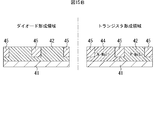
先ず、図1Aに示すように、半導体基板として、例えばシリコン基板11を用意する。以下の各図において、左側がダイオード形成領域、右側がトランジスタ形成領域をそれぞれ示している。
First, as shown in FIG. 1A, for example, a
続いて、図1Bに示すように、p型ウェル12を形成する。
詳細には、シリコン基板11の表面にp型不純物をイオン注入し、シリコン基板11の表層にp型ウェル12を形成する。Subsequently, as shown in FIG. 1B, the p-
Specifically, p-type impurities are ion-implanted into the surface of the
続いて、図1Cに示すように、n型ウェル14を形成する。
詳細には、先ず、シリコン基板11の表面にレジストを塗布し、リソグラフィーによりレジストを加工する。以上により、トランジスタ形成領域において、シリコン基板11の表面のn型ウェル形成領域を露出する開口13aを有するレジストマスク13が形成される。
次に、レジストマスク13を用いて、開口13aから露出するシリコン基板11の部分にn型不純物をイオン注入する。これにより、トランジスタ形成領域には、シリコン基板11の表層に、p型ウェル12と隣接するn型ウェル14が形成される。レジストマスク13は、ウェット処理又はアッシング処理により除去される。Then, as shown in FIG. 1C, the n-
Specifically, first, a resist is applied to the surface of the
Next, using the resist
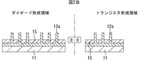
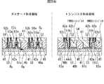
続いて、図2A〜図2Cに示すように、シリコン基板11をフィン状に加工した後、STI素子分離構造15を形成する。図2Cが平面図であり、図2Aが図2C中の破線I−I(横方向(X方向))に沿った断面図、図2Bが図2C中の破線II−II(縦方向(Y方向))に沿った断面図である。
詳細には、先ず、シリコン基板11のp型ウェル12及びn型ウェル14の部分をリソグラフィー及びドライエッチングにより、ストライプ状に並ぶフィン状に加工する。p型ウェル12のフィン状部分をフィン12a、n型ウェル14のフィン状部分をフィン14aとする。図2Cのダイオード形成領域では、フィン12aが図面上側で3本、図面下側で3本の群として配置されているが、その本数は3本に限られない。例えばフィン12aの群の本数が、1本や2本であってもよいし、例えば7本のような、3本より大きい数の本数であってもよい。また、ダイオード形成領域と同様に、図2Cのトランジスタ領域のフィン12a及び14aのそれぞれの本数も3本に限られず任意である。Subsequently, as shown in FIGS. 2A to 2C, after the
Specifically, first, the portions of the p-
次に、フィン12a,14a間を埋め込むように、シリコン基板11上に絶縁膜、例えばシリコン酸化膜をCVD法等により堆積する。堆積したシリコン酸化膜をエッチバックで平坦化することにより、シリコン基板11上でフィン12a,14a間を所定厚のシリコン酸化膜で埋め込むSTI素子分離構造15が形成される。
Next, an insulating film, for example, a silicon oxide film is deposited on the
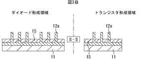
続いて、図3A〜図3Cに示すように、ダミーゲート絶縁膜16及びダミーゲート電極17を形成する。図3Cが平面図であり、図3Aが図3C中の破線I−Iに沿った断面図、図3Bが図3C中の破線II−IIに沿った断面図である。
詳細には、先ず、シリコン基板11の表面を熱酸化し、熱酸化膜を形成する。
次に、シリコン基板11の全面にCVD法等により多結晶シリコン膜を堆積する。リソグラフィー及びドライエッチングにより熱酸化膜及び多結晶シリコン膜をゲート形状に加工する。以上により、フィン12a,14aの長手方向に直交するゲート形状に、ダミーゲート絶縁膜16及びダミーゲート電極17が形成される。Subsequently, as shown in FIGS. 3A to 3C, a dummy
Specifically, first, the surface of the
Next, a polycrystalline silicon film is deposited on the entire surface of the
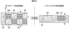
続いて、図4A〜図4Cに示すように、ダイオード形成領域にはn型領域19aを、トランジスタ形成領域にはn型ソース/ドレイン領域19bをそれぞれ形成する。図4Cが平面図であり、図4Aが図4C中の破線I−Iに沿った断面図、図4Bが図4C中の破線II−IIに沿った断面図である。
詳細には、先ず、シリコン基板11の表面にレジストを塗布し、リソグラフィーによりレジストを加工する。以上により、ダイオード形成領域ではフィン12aにおけるn型領域の形成部位を露出する開口18aを、トランジスタ形成領域ではフィン12aにおけるn型ソース/ドレイン領域の形成部位を露出する開口18aを有するレジストマスク18が形成される。
次に、レジストマスク18を用いて、開口18aから露出するフィン12aの部分にn型不純物をイオン注入する。イオン注入は、n型ウェル14のn型不純物濃度よりも高濃度となる条件で行われる。これにより、ダイオード形成領域ではフィン12aにn型領域19aが、トランジスタ形成領域ではフィン12aにn型ソース/ドレイン領域19bがそれぞれ形成される。レジストマスク18は、ウェット処理又はアッシング処理により除去される。Subsequently, as shown in FIGS. 4A to 4C, an n-
Specifically, first, a resist is applied to the surface of the
Next, using the resist
なお、n型領域19a及びn型ソース/ドレイン領域19bを形成する代わりに、フィン12aの一部を除去し、n型半導体層をエピタキシャル成長するようにしても良い。
Instead of forming the n-
続いて、図5A〜図5Cに示すように、ダイオード形成領域にはp型領域22aを、トランジスタ形成領域にはp型ソース/ドレイン領域22bをそれぞれ形成する。図5Cが平面図であり、図5Aが図5C中の破線I−Iに沿った断面図、図5Bが図5C中の破線II−IIに沿った断面図である。
詳細には、先ず、シリコン基板11の表面にレジストを塗布し、リソグラフィーによりレジストを加工する。以上により、ダイオード形成領域ではフィン12aにおけるp型領域の形成部位を露出する開口21aを、トランジスタ形成領域ではフィン14aにおけるp型ソース/ドレイン領域の形成部位を露出する開口21aを有するレジストマスク21が形成される。
次に、レジストマスク21を用いて、開口21aから露出するフィン12a,14aの部分にp型不純物をイオン注入する。イオン注入は、p型ウェル12のp型不純物濃度よりも高濃度となる条件で行われる。以上により、ダイオード形成領域ではフィン12aにn型領域22aが、トランジスタ形成領域ではフィン14aにp型ソース/ドレイン領域22bがそれぞれ形成される。レジストマスク21は、ウェット処理又はアッシング処理により除去される。Subsequently, as shown in FIGS. 5A to 5C, a p-
Specifically, first, a resist is applied to the surface of the
Next, using the resist
なお、p型領域22a及びp型ソース/ドレイン領域22bを形成する代わりに、フィン12a,14aの一部を除去し、p型半導体層をエピタキシャル成長するようにしても良い。
Instead of forming the p-
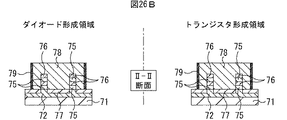
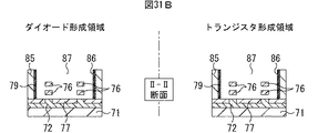
続いて、図6A〜図6Cに示すように、ゲート絶縁膜24及びゲート電極25を形成する。図6Cが平面図であり、図6Aが図6C中の破線I−Iに沿った断面図、図6Bが図6C中の破線II−IIに沿った断面図である。図6Cでは、層間絶縁膜23の図示を省略する。
詳細には、先ず、シリコン基板11の全面を覆う絶縁膜、例えばシリコン酸化膜をCVD法等により堆積し、層間絶縁膜23を形成する。化学機械研磨(Chemical Mechanical Polishing:CMP)法により、層間絶縁膜23を、ダミーゲート電極17の上面が露出するまで平坦化する。その後、例えばウェットエッチングによりダミーゲート絶縁膜16及びダミーゲート電極17を選択的に除去する。
次に、ダミーゲート絶縁膜16及びダミーゲート電極17を除去したことにより層間絶縁膜23に形成された開口内に、ゲート絶縁膜24及びゲート電極25を形成する。ゲート絶縁膜24は高誘電率材料を用いて、ゲート電極25は金属材料を用いて形成される。
Subsequently, as shown in FIGS. 6A to 6C, a
Specifically, first, an insulating film covering the entire surface of the
Next, the
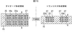
続いて、図7A〜図7Cに示すように、ローカルインターコネクト27を形成する。図7Cが平面図であり、図7Aが図7C中の破線I−Iに沿った断面図、図7Bが図7C中の破線II−IIに沿った断面図である。図7Cでは、層間絶縁膜23,26の図示を省略する。
詳細には、先ず、層間絶縁膜23上に絶縁膜、例えばシリコン酸化膜をCVD法等により堆積し、層間絶縁膜26を形成する。
次に、リソグラフィー及びドライエッチングにより層間絶縁膜23,26を加工する。ダイオード形成領域では、層間絶縁膜23,26にn型領域19a,22aの表面の一部を露出する開口が形成される。トランジスタ形成領域では、層間絶縁膜23,26にn型ソース/ドレイン領域19b,22bの表面の一部を露出する開口と、層間絶縁膜26にゲート電極25の表面の一部を露出する開口とが形成される。
次に、各開口を埋め込むように、層間絶縁膜26上に金属材料、例えばチタン又は窒化チタン27aを下地としてタングステン27bを堆積する。CMP法により、堆積されたチタン又は窒化チタン27a及びタングステン27bを層間絶縁膜26の上面が露出するまで平坦化する。以上により、ダイオード形成領域では、n型領域19a又は22aと接続されたローカルインターコネクト27が形成される。トランジスタ形成領域では、n型ソース/ドレイン領域19b又は22b、ゲート電極25と接続されたローカルインターコネクト27がそれぞれ形成される。Subsequently, as shown in FIGS. 7A to 7C, the
Specifically, first, an insulating film, for example, a silicon oxide film is deposited on the
Next, the
Next, a
続いて、図8、図9A〜図9Cに示すように、第1配線層10aを形成する。図9Aがダイオード形成領域の平面図であり、図8がトランジスタ形成領域の平面図である。図9Bが図9A中の破線I−Iに沿った断面図、図9Cが図9A中の破線II−IIに沿った断面図である。図9Aでは、層間絶縁膜23,26,28等の図示を省略する。
本実施形態では、ダイオード形成領域では、いわゆるデュアルダマシン法を用いて第1配線層10aを形成する。詳細には、先ず、例えばシリコン酸化膜の層間絶縁膜28をリソグラフィー及びドライエッチングにより加工し、層間絶縁膜28に配線溝と、ビア孔及び配線溝が一体となった複合溝とを形成する。Subsequently, as shown in FIGS. 8 and 9A to 9C, the
In the present embodiment, the
次に、配線溝及び複合溝を埋め込むように、層間絶縁膜28上に金属材料、例えば窒化タンタルを下地とする銅を堆積する。形成される窒化タンタル及び銅は、配線溝については、窒化タンタル32a(又は窒化タンタル33a)、銅32b(又は銅33b)とする。複合溝については、一体形成された窒化タンタル32a及び窒化タンタル29a(又は窒化タンタル33a及び窒化タンタル29a)、一体形成された銅32b及び銅29b(又は銅33b及び銅29b)とする。CMP法により、堆積された窒化タンタル及び銅を層間絶縁膜28の上面が露出するまで平坦化する。以上により、層間絶縁膜28内に配線32(又は配線33)と、配線32とビア29が一体形成された配線構造(又は配線33とビア29が一体形成された配線構造)を備えた第1配線層10aが形成される。
トランジスタ形成領域では、図8のように、層間絶縁膜28内にビア29と同時に配線29Aが形成され、層間絶縁膜28の表面に配線29Aの表面が露出する。Next, a metal material, for example, copper based on tantalum nitride is deposited on the
In the transistor formation region, as shown in FIG. 8, a
図9Aのように、配線32及び上記の配線構造は、縦方向に並ぶ複数のゲート電極25の上方で延在する部分と、両側にn型領域19aが配されたローカルインターコネクト27上のコンタクトプラグ29と接続された部分と、上記の双方の部分を接続する部分とが一体形成されて構成されている。配線33及び上記の配線構造は、縦方向に並ぶ複数のゲート電極25の上方で延在する部分と、両側にp型領域22aが配されたローカルインターコネクト27上のコンタクトプラグ29と接続された部分と、上記の双方の部分を接続する部分とが一体形成されて構成されている。
As shown in FIG. 9A, the
本実施形態では、図9Aのようなレイアウトに替わって、例えば図10Aのようなレイアウトに構成しても良い。この場合にも、上記と同様に、デュアルダマシン法が用いられる。図10Aでは、横方向の一行分のゲート電極25及びローカルインターコネクト27が一行置きに半ピッチずれたレイアウトとされている。この場合、縦方向に沿って、n型領域19aの一部とp型領域22aの一部とが交互に配置されている。このようなレイアウトに構成することにより、配線34,35をそれぞれ一方向(ここでは縦方向)のみに延在する形状に形成することができる。具体的には、配線34,35は、縦方向に交互に並ぶ複数のゲート電極25の上方及びローカルインターコネクト27と接続されて延在している。この構成では、配線のパターニング時の露光が容易となる(ダブルパターニングを適用し易い。)。
In the present embodiment, the layout as shown in FIG. 9A may be replaced with a layout as shown in FIG. 10A. Also in this case, the dual damascene method is used as in the above. In FIG. 10A, the layout is such that the
図10Aでは、ダイオード上の縦方向の配線34,35それぞれを接続する横方向の配線34,35が図示されているが、例えば縦方向の配線34,35を多層配線構造の1層目、横方向の配線34,35を2層目に配置しても良い。1層目の配線34,35と2層目の配線34,35は、それぞれビアにより接続しても良い。このように配線を形成することにより、例えば横方向に延在する配線を持つ配線層と、縦方向に延在する配線を持つ配線層とを例えば交互に積層する多層配線構造とすることが容易となる。そのため、各配線層で配線のパターニング時にダブルパターニングを適用し易いものとなる。
In FIG. 10A, the
また、図10Bのようなレイアウトに構成することも考えられる。この場合、ビア29をp型、n型の導電型ごとに縦方向(Y方向)へシフトして配置し、横方向に延在する配線34,35で導電型ごとのビア29を接続し、配線34,35を縦方向に延在させる。この構成でも、配線のパターニング時の露光が容易となる(ダブルパターニングを適用し易い。)。この場合、配線34,35の横方向の延在部分と縦方向の延在部分とを異なる層として形成しても良い。
It is also possible to configure the layout as shown in FIG. 10B. In this case, the
しかる後、図11Aに示すように、複数の配線層が積層形成され、最上層に接続パッド36が形成される。
詳細には、第1配線層10a上に複数層、例えば4層(第2配線層10b、第3配線層10c、第4配線層10d、第5配線層10e)が積層されて多層配線構造とされる。最上層には、多層配線構造と接続された、アルミニウム等を材料とする接続パッド36が形成される。ここで、接続パッド36は、図11Bに示すように、ダイオード形成領域及びトランジスタ形成領域の上方に、平面視でダイオード形成領域及びトランジスタ形成領域を内包するように配されている。図11Bでは、半導体チップの外周部分を37で示している。なお、配線層の数は4層に限られず、それ以上、例えば10層以上あっても良い。また、ダイオード形成領域の第1のダイオードDa及び第2のダイオードDbを、上方の接続パッド36と電気的に接続させ、図13の回路構成図のようにしても良い。
以上により、本実施形態による半導体装置が形成される。Thereafter, as shown in FIG. 11A, a plurality of wiring layers are laminated and formed, and the
More specifically, a plurality of layers, for example, four layers (
As described above, the semiconductor device according to the present embodiment is formed.
本実施形態では、ダイオード形成領域には、図9Aのように、ESD保護ダイオードとして、第1のダイオードDA及び第2のダイオードDBが形成され、両者が並列に接続されている。トランジスタ形成領域には、PMOSトランジスタ及びNMOSトランジスタが形成されている。In the present embodiment, as shown in FIG. 9A, a first diode D A and a second diode D B are formed as ESD protection diodes in the diode formation region, and both are connected in parallel. A PMOS transistor and an NMOS transistor are formed in the transistor formation region.
第1のダイオードDAは、ゲート電極25を有し、ゲート電極25の近傍におけるフィン12aに電流経路が形成されるゲート型ダイオードである。第2のダイオードDBは、STI素子分離構造15を有し、STI素子分離構造15の近傍におけるフィン12aに電流経路が形成されるSTI型ダイオードである。The first diode D A is a gate-type diode that has a
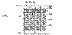
図12は、本実施形態における半導体装置のダイオード形成領域のレイアウト構成を示す概略平面図である。
ダイオード形成領域では、複数のゲート電極25が行列状に配列しており、横方向及び縦方向の各々について、p型領域22a及びn型領域19aが交互に、言わば市松模様状に配置されている。図12では便宜上、ゲート電極25及びp型領域22aを有する領域をp型区域1、ゲート電極25及びn型領域19aを有する領域をn型区域2と記す。横方向及び縦方向について区域1,2が交互に配置されるため、p型とn型のイオン注入の境界部位が多くなるが、当該境界部位は全てSTI素子分離構造15に位置しており、製造時のマスクずれの許容範囲が大きい。
FIG. 12 is a schematic plan view showing the layout configuration of the diode formation region of the semiconductor device in this embodiment.
In the diode formation region, a plurality of
第1のダイオードDAと第2のダイオードDBとでは、p型領域22a及びn型領域19aを共有している。第1のダイオードDAは、横方向に配列しており、ゲート電極25とその両側のp型領域22a及びn型領域19aとを有して構成される。第2のダイオードDBは、縦方向に配列しており、p型領域22a及びn型領域19aと、これらの間のSTI素子分離構造15とを有して構成される。The first diode D A and the second diode D B share the p-
本実施形態による半導体装置の回路構成を図13に示す。図13では、横方向に並ぶ複数の第1のダイオードDAを代表してダイオードAn(n=1,2,・・・)と記す。縦方向に並ぶ複数の第2のダイオードDBを代表してダイオードBn(n=1,2,・・・)と記す。本実施形態では、ダイオードAn,Bnが並列に接続されている。そのため、I/O端子からサージ電流が流れた場合、サージ電流は、CMOSトランジスタ(p型MOSトランジスタ及びn型MOSトランジスタ)を通ることが抑制され、2種類の電流経路P1,P2を通ることになる。電流経路P1は、ダイオードAn、パワーレールクランプ、VSS端子を通る経路である。電流経路P2は、ダイオードBn、パワーレールクランプ、VSS端子を通る経路である。この構成により、従来技術のように、ESD保護ダイオードがゲート型ダイオードのみ又はSTI型ダイオードのみの場合と比較して電流経路が増加し、ESD保護ダイオードの低抵抗化が実現する。また、本実施形態のように、p型区域1及びn型区域2を交互に配置することにより、従来技術の場合と比較して、ESD保護ダイオードの占有面積を低減させることができる。The circuit configuration of the semiconductor device according to the present embodiment is shown in FIG. In FIG. 13, the plurality of first diodes D A arranged in the horizontal direction are represented as diodes An (n=1, 2,...) As a representative. The plurality of second diodes D B arranged in the vertical direction are represented as diodes Bn (n=1, 2,...) As a representative. In this embodiment, the diodes An and Bn are connected in parallel. Therefore, when a surge current flows from the I/O terminal, the surge current is suppressed from passing through the CMOS transistor (p-type MOS transistor and n-type MOS transistor), and the surge current passes through two types of current paths P1 and P2. Become. The current path P1 is a path that passes through the diode An, the power rail clamp, and the VSS terminal. The current path P2 is a path that passes through the diode Bn, the power rail clamp, and the VSS terminal. With this configuration, the current path is increased as compared with the case where the ESD protection diode is only the gate type diode or the STI type diode as in the prior art, and the resistance of the ESD protection diode is reduced. Further, by alternately arranging the p-
以上説明したように、本実施形態によれば、低抵抗化及び占有面積の低減を図るも、大きなサージ電流に十分に対処することができるESD保護ダイオードを備えた信頼性の高い半導体装置が実現する。 As described above, according to the present embodiment, it is possible to realize a highly reliable semiconductor device including an ESD protection diode that can sufficiently cope with a large surge current while achieving a reduction in resistance and a reduction in occupied area. To do.
(第2の実施形態)
以下、第2の実施形態について説明する。本実施形態では、いわゆる縦型トランジスタ構造を適用したESD保護ダイオードを備えた半導体装置を開示する。図14A〜図22は、本実施形態による半導体装置の製造方法を示す模式図である。(Second embodiment)
The second embodiment will be described below. In this embodiment, a semiconductor device including an ESD protection diode to which a so-called vertical transistor structure is applied is disclosed. 14A to 22 are schematic views illustrating the method of manufacturing the semiconductor device according to the present embodiment.
先ず、図14Aに示すように、半導体基板として、例えばシリコン基板41を用意する。以下の各図において、左側がダイオード形成領域、右側がトランジスタ形成領域をそれぞれ示している。
First, as shown in FIG. 14A, for example, a
続いて、図14Bに示すように、p型ウェル42を形成する。
詳細には、シリコン基板41の表面にp型不純物をイオン注入し、シリコン基板41の表層にp型ウェル42を形成する。Subsequently, as shown in FIG. 14B, the p-
Specifically, p-type impurities are ion-implanted into the surface of the
続いて、図15Aに示すように、n型ウェル44を形成する。
詳細には、先ず、シリコン基板41の表面にレジストを塗布し、リソグラフィーによりレジストを加工する。以上により、トランジスタ形成領域において、シリコン基板41の表面のn型ウェル形成領域を露出する開口43aを有するレジストマスク43が形成される。
次に、レジストマスク43を用いて、開口43aから露出するシリコン基板41の部分にn型不純物をイオン注入する。これにより、トランジスタ形成領域には、シリコン基板41の表層に、p型ウェル42と隣接するn型ウェル44が形成される。レジストマスク43は、ウェット処理又はアッシング処理により除去される。Subsequently, as shown in FIG. 15A, the n-
Specifically, first, a resist is applied to the surface of the
Next, using the resist
続いて、図15Bに示すように、STI素子分離構造45を形成する。
詳細には、シリコン基板41の素子分離領域をリソグラフィー及びドライエッチングにより加工し、素子分離領域に溝を形成する。溝内を埋め込むように、シリコン基板41上に絶縁膜、例えばシリコン酸化膜をCVD法等により堆積する。堆積したシリコン酸化膜をエッチバックで平坦化することにより、シリコン基板41の表層に、素子分離領域の溝内をシリコン酸化膜で埋め込むSTI素子分離構造45が形成される。Subsequently, as shown in FIG. 15B, the STI
Specifically, the element isolation region of the
続いて、図16Aに示すように、シリコン基板41を柱状に加工する。
詳細には、シリコン基板41上に例えばシリコン窒化膜からなるハードマスク46を形成し、このハードマスク46を用いて、シリコン基板41のp型ウェル42及びn型ウェル44の部分をドライエッチングする。これにより、シリコン基板41を柱状に加工する。p型ウェル42の柱状部分を柱状突起42a、n型ウェル44の柱状部分を柱状突起44aとする。Subsequently, as shown in FIG. 16A, the
Specifically, a
続いて、図16Bに示すように、ダイオード形成領域にはp型領域48aを、トランジスタ形成領域にはp型ソース/ドレイン領域48bをそれぞれ形成する。
詳細には、先ず、シリコン基板41の表面にレジストを塗布し、リソグラフィーによりレジストを加工する。以上により、ダイオード形成領域では柱状突起42aの周辺におけるp型領域の形成部位を露出する開口47aを、トランジスタ形成領域では柱状突起44aの周辺におけるp型ソース/ドレイン領域の形成部位を露出する開口47aを有するレジストマスク47が形成される。
次に、レジストマスク47を用いて、開口47aから露出する柱状突起42aの周辺部分にp型不純物をイオン注入する。イオン注入は、p型ウェル42のp型不純物濃度よりも高濃度となる条件で行われる。これにより、ダイオード形成領域では柱状突起42aの周辺にp型領域48aが、トランジスタ形成領域では柱状突起44aの周辺にp型ソース/ドレイン領域48bがそれぞれ形成される。レジストマスク47は、ウェット処理又はアッシング処理により除去される。Subsequently, as shown in FIG. 16B, a p-
Specifically, first, a resist is applied to the surface of the
Next, using the resist
続いて、図17Aに示すように、ダイオード形成領域にはn型領域51aを、トランジスタ形成領域にはn型ソース/ドレイン領域51bをそれぞれ形成する。
詳細には、先ず、シリコン基板41の表面にレジストを塗布し、リソグラフィーによりレジストを加工する。以上により、ダイオード形成領域では柱状突起42aの周辺におけるn型領域の形成部位を露出する開口49aを、トランジスタ形成領域では柱状突起42aの周辺におけるn型ソース/ドレイン領域の形成部位を露出する開口49aを有するレジストマスク49が形成される。
次に、レジストマスク49を用いて、開口49aから露出する柱状突起42aの周辺部分にn型不純物をイオン注入する。イオン注入は、n型ウェル44のn型不純物濃度よりも高濃度となる条件で行われる。これにより、ダイオード形成領域では柱状突起42aの周辺にn型領域51aが、トランジスタ形成領域では柱状突起42aの周辺にn型ソース/ドレイン領域51bがそれぞれ形成される。レジストマスク49は、ウェット処理又はアッシング処理により除去される。Subsequently, as shown in FIG. 17A, an n-
Specifically, first, a resist is applied to the surface of the
Next, using the resist
続いて、図17Bに示すように、ゲート絶縁膜52を形成する。
詳細には、シリコン基板41の表面を熱酸化する。このとき、ダイオード形成領域では、柱状突起42aの側面からp型領域48aの表面又はn型領域51aの表面に架けてゲート絶縁膜52が形成される。トランジスタ形成領域では、柱状突起44aの側面からp型ソース/ドレイン領域48bの表面に架けて、及び柱状突起42aの側面からn型ソース/ドレイン領域51bの表面に架けて、それぞれゲート絶縁膜52が形成される。Subsequently, as shown in FIG. 17B, a
Specifically, the surface of the
続いて、図18Aに示すように、ゲート電極53を形成する。
詳細には、シリコン基板41の全面に、CVD法により例えば多結晶シリコン膜を堆積し、その全面をエッチバックする。多結晶シリコン膜は、ゲート絶縁膜52を介した柱状突起42a,44aの側面のみに残存し、ゲート電極53が形成される。このとき、トランジスタ形成領域では、柱状突起42a,44aの側面とSTI素子分離構造45との間を埋め込むように、ゲート電極53よりも厚い多結晶シリコン膜53aを残存させる。Subsequently, as shown in FIG. 18A, the
In detail, for example, a polycrystalline silicon film is deposited on the entire surface of the
続いて、図18Bに示すように、層間絶縁膜54を形成する。
詳細には、シリコン基板41の全面に絶縁膜、例えばシリコン酸化膜をCVD法等により堆積する。CMP法により、このシリコン酸化膜をハードマスク46の上面が露出するまで平坦化する。以上により、表面からハードマスク46の上面が露出する層間絶縁膜54が形成される。Subsequently, as shown in FIG. 18B, an
Specifically, an insulating film, for example, a silicon oxide film is deposited on the entire surface of the
続いて、図19Aに示すように、Si層55を形成する。
詳細には、先ず、例えばウェットエッチングによりハードマスク46を選択的に除去する。その後、層間絶縁膜54の表面下で露出する柱状突起42a,44aの上面から半導体層、ここではSi層55をエピタキシャル成長する。Subsequently, as shown in FIG. 19A, a
Specifically, first, the
続いて、図19Bに示すように、ダイオード形成領域にはp型領域57aを、トランジスタ形成領域にはp型ソース/ドレイン領域57bをそれぞれ形成する。
詳細には、先ず、層間絶縁膜54の表面にレジストを塗布し、リソグラフィーによりレジストを加工する。以上により、ダイオード形成領域では柱状突起42a上のSi層55の上面を露出する開口56aを、トランジスタ形成領域では柱状突起44a上のSi層55の上面を露出する開口56aを有するレジストマスク56が形成される。
次に、レジストマスク56を用いて、開口56aから露出する柱状突起42a,44aの上面部分にp型不純物をイオン注入する。以上により、ダイオード形成領域ではSi層55にp型領域57aが、トランジスタ形成領域ではSi層55にp型ソース/ドレイン領域57bがそれぞれ形成される。レジストマスク56は、ウェット処理又はアッシング処理により除去される。Subsequently, as shown in FIG. 19B, a p-
Specifically, first, a resist is applied to the surface of the
Next, using the resist
続いて、図20Aに示すように、ダイオード形成領域にはn型領域59aを、トランジスタ形成領域にはn型ソース/ドレイン領域59bをそれぞれ形成する。
詳細には、先ず、層間絶縁膜54の表面にレジストを塗布し、リソグラフィーによりレジストを加工する。以上により、ダイオード形成領域及びトランジスタ形成領域の各々において、柱状突起42a上のSi層55の上面を露出する開口58aを有するレジストマスク58が形成される。
次に、レジストマスク58を用いて、開口58aから露出する柱状突起42aの上面部分にn型不純物をイオン注入する。以上により、ダイオード形成領域ではSi層55にn型領域59aが、トランジスタ形成領域ではSi層55にn型ソース/ドレイン領域59bがそれぞれ形成される。レジストマスク58は、ウェット処理又はアッシング処理により除去される。Subsequently, as shown in FIG. 20A, an n-
Specifically, first, a resist is applied to the surface of the
Next, using the resist
続いて、図20Bに示すように、コンタクトプラグ62a〜62cを形成する。
詳細には、先ず、層間絶縁膜54上に絶縁膜、例えばシリコン酸化膜をCVD法等により堆積し、層間絶縁膜61を形成する。
次に、リソグラフィー及びドライエッチングにより、ゲート絶縁膜52及び層間絶縁膜54,61を加工する。これにより、ダイオード形成領域では、層間絶縁膜61にp型領域57a及びn型領域59aの表面の一部を露出する開口と、ゲート絶縁膜52及び層間絶縁膜54,61にp型領域48a及びn型領域51aの表面の一部を露出する開口とが形成される。トランジスタ形成領域では、層間絶縁膜61にp型ソース/ドレイン領域57b及びn型ソース/ドレイン領域59bの表面の一部を露出する開口と、ゲート絶縁膜52及び層間絶縁膜54,61にp型ソース/ドレイン領域48b及びn型ソース/ドレイン領域51bの表面の一部を露出する開口と、層間絶縁膜54,61に多結晶シリコン膜53aの表面の一部を露出する開口とが形成される。
次に、各開口を埋め込むように、層間絶縁膜61上に金属材料、例えばチタン又は窒化チタンを下地とするタングステンを堆積する。CMP法により、堆積されたチタン又は窒化チタン及びタングステンを層間絶縁膜61の上面が露出するまで平坦化する。以上により、ダイオード形成領域では、p型領域57a及びn型領域59aとそれぞれ接続されたコンタクトプラグ62aと、p型領域48a及びn型領域51aとそれぞれ接続されたコンタクトプラグ62bとが形成される。トランジスタ形成領域では、p型ソース/ドレイ領域57b及びn型ソース/ドレイン領域59bとそれぞれ接続されたコンタクトプラグ62aと、p型ソース/ドレイン領域48b及びn型ソース/ドレイン領域51bとそれぞれ接続されたコンタクトプラグ62bと、多結晶シリコン膜53aと接続されたコンタクトプラグ62cとが形成される。図21は、本実施形態による半導体装置のダイオード形成領域のレイアウト構成を示す概略平面図である。図21では、層間絶縁膜54,61及びコンタクトプラグ62a〜62cの図示を省略する。Subsequently, as shown in FIG. 20B, contact plugs 62a to 62c are formed.
Specifically, first, an insulating film, for example, a silicon oxide film is deposited on the
Next, the
Next, a metal material, for example, tungsten based on titanium or titanium nitride is deposited on the
しかる後、第1の実施形態と同様に、多層配線構造及び接続パッドを形成し、本実施形態による半導体装置とされる。接続パッドは、ダイオード形成領域及びトランジスタ形成領域の上方に、平面視でダイオード形成領域及びトランジスタ形成領域を内包するように配される。 Then, similarly to the first embodiment, the multilayer wiring structure and the connection pad are formed, and the semiconductor device according to the present embodiment is obtained. The connection pad is arranged above the diode formation region and the transistor formation region so as to include the diode formation region and the transistor formation region in plan view.
本実施形態においても、第1の実施形態と同様に、多層配線構造の第1配線層を図22のように形成しても良い。この場合、横方向の一行分のp型領域57a及びn型領域59aが一行置きに半ピッチずれたレイアウトとされている。このようなレイアウトに構成することにより、第1配線層の配線63,64をそれぞれ一方向(ここでは縦方向)のみに延在する形状に形成することができる。具体的には、配線63,64は、縦方向に交互に並ぶ複数(図示の例では2つ)のp型領域57a及び複数(図示の例では2つ)のコンタクトプラグ65と接続されて、又は縦方向に交互に並ぶ複数(図示の例では2つ)のn型領域59a及び複数(図示の例では2つ)のコンタクトプラグ65と接続されて延在している。この構成では、配線のパターニング時の露光が容易となる(ダブルパターニングを適用し易い。)。
Also in this embodiment, as in the first embodiment, the first wiring layer of the multilayer wiring structure may be formed as shown in FIG. In this case, the layout is such that the p-
本実施形態では、ダイオード形成領域には、図20B及び図21のように、ESD保護ダイオードとして、第1のダイオードDA及び第2のダイオードDBが形成され、両者が並列に接続されている。トランジスタ形成領域には、図20Bのように、PMOSトランジスタ及びNMOSトランジスタが形成されている。In the present embodiment, as shown in FIGS. 20B and 21, in the diode formation region, a first diode D A and a second diode D B are formed as ESD protection diodes, and both are connected in parallel. .. A PMOS transistor and an NMOS transistor are formed in the transistor formation region as shown in FIG. 20B.
第1のダイオードDAは、ゲート電極53を有し、ゲート電極53の近傍における柱状突起42aに電流経路が形成されるゲート型ダイオードである。第2のダイオードDBは、STI素子分離構造45を有し、STI素子分離構造45の近傍におけるp型ウェル42に電流経路が形成されるSTI型ダイオードである。
The first diode D A is a gate type diode having a
図21のように、ダイオード形成領域では、横方向及び縦方向の各々について、p型領域48a及びn型領域51aが交互に、言わば市松模様状に配置されている。1つのp型領域48aでは、上面にn型領域59aが、側面にゲート絶縁膜52を介したゲート電極53が形成された柱状突起42aが所定数、例えば4本形成されている。1つのn型領域51aでは、上面にp型領域57aが、側面にゲート絶縁膜52を介したゲート電極53が形成された柱状突起42aが所定数、例えば4本形成されている。
As shown in FIG. 21, in the diode formation region, the p-
第1のダイオードDAと第2のダイオードDBとでは、p型領域48a又はn型領域51aを共有している。第1のダイオードDAは、横方向及び縦方向に配列しており、ゲート電極53と柱状突起42aの周囲のp型領域48a(又はn型領域51a)及び上面のn型領域59a(又はp型領域57a)を有して構成される。第2のダイオードDBは、横方向及び縦方向に配列しており、p型領域48a及びn型領域51aと、これらの間のSTI素子分離構造45を有して構成される。The first diode D A and the second diode D B share the p-
本実施形態の半導体装置では、ダイオード形成領域において、図21のように、横方向及び縦方向の双方について、ゲート型ダイオードである複数の第1のダイオードDA及びSTI型ダイオードである複数の第2のダイオードDBが配設されている。第1のダイオードDA及び第2のダイオードDBは並列に接続されている。この構成により、サージ電流が生じた場合には、第1の実施形態の図13と同様に、2種類の電流経路が形成される。そのため、従来技術のように、ESD保護ダイオードがゲート型ダイオードのみ又はSTI型ダイオードのみの場合と比較して電流経路が増加し、ESD保護ダイオードの低抵抗化が実現する。また、本実施形態のように、p型領域48a及びn型領域51aを交互に配置することにより、従来技術の場合と比較して、ESD保護ダイオードの占有面積を低減させることができる。In the semiconductor device according to the present embodiment, in the diode formation region, as shown in FIG. 21, a plurality of first diodes D A that are gate type diodes and a plurality of first diodes that are STI type diodes are provided in both the horizontal and vertical directions. Two diodes D B are arranged. The first diode D A and the second diode D B are connected in parallel. With this configuration, when a surge current is generated, two types of current paths are formed as in the case of FIG. 13 of the first embodiment. Therefore, as in the prior art, the current path is increased as compared with the case where the ESD protection diode is only the gate type diode or the STI type diode, and the resistance of the ESD protection diode is reduced. Further, by alternately disposing the p-
以上説明したように、本実施形態によれば、低抵抗化及び占有面積の低減を図るも、大きなサージ電流に十分に対処することができるESD保護ダイオードを備えた信頼性の高い半導体装置が実現する。 As described above, according to the present embodiment, it is possible to realize a highly reliable semiconductor device including an ESD protection diode that can sufficiently cope with a large surge current while achieving a reduction in resistance and a reduction in occupied area. To do.
(第3の実施形態)
以下、第3の実施形態について説明する。本実施形態では、いわゆるナノワイヤ構造を適用したESD保護ダイオードを備えた半導体装置を開示する。図23A〜図38は、本実施形態による半導体装置の製造方法を示す模式図である。(Third Embodiment)
The third embodiment will be described below. This embodiment discloses a semiconductor device including an ESD protection diode to which a so-called nanowire structure is applied. 23A to 38 are schematic views showing the method of manufacturing the semiconductor device according to the present embodiment.
先ず、図23Aに示すように、半導体基板として、例えばシリコン基板71を用意する。以下の各図において、左側がダイオード形成領域、右側がトランジスタ形成領域をそれぞれ示している。
First, as shown in FIG. 23A, for example, a
続いて、図23Bに示すように、p型ウェル72を形成する。
詳細には、シリコン基板71の表面にp型不純物をイオン注入し、シリコン基板71の表層にp型ウェル72を形成する。Subsequently, as shown in FIG. 23B, a p-
Specifically, p-type impurities are ion-implanted into the surface of the
続いて、図23Cに示すように、n型ウェル74を形成する。
詳細には、先ず、シリコン基板71の表面にレジストを塗布し、リソグラフィーによりレジストを加工する。以上により、トランジスタ形成領域において、シリコン基板71の表面のn型ウェル形成領域を露出する開口73aを有するレジストマスク73が形成される。
次に、レジストマスク73を用いて、開口73aから露出するシリコン基板71の部分にn型不純物をイオン注入する。これにより、トランジスタ形成領域には、シリコン基板71の表層に、p型ウェル72と隣接するn型ウェル74が形成される。レジストマスク73は、ウェット処理又はアッシング処理により除去される。Subsequently, as shown in FIG. 23C, an n-
Specifically, first, a resist is applied to the surface of the
Next, using the resist
続いて、図24Aに示すように、SiGe層75及びSi層76を交互に積層する。
詳細には、シリコン基板71上に、2種の半導体層、ここではSiGe層75及びSi層76を交互に複数層、例えば2層ずつ積層する。なお、積層する層数は2層ずつに限られない。例えばSiGe層75とSi層76とを1層ずつ積層しても良いし、2層よりも多い層数ずつ積層しても良い。また、Si層76、SiGe層75の順に積層しても良い。Subsequently, as shown in FIG. 24A, SiGe layers 75 and Si layers 76 are alternately laminated.
More specifically, two types of semiconductor layers, here, a
続いて、図24B〜図24Dに示すように、シリコン基板71をフィン状に加工した後、STI素子分離構造77を形成する。図24Dが平面図であり、図4Bが図24D中の破線I−Iに沿った断面図、図24Cが図24D中の破線II−IIに沿った断面図である。
詳細には、先ず、シリコン基板71のp型ウェル12及びn型ウェル14の一部と、SiGe層75及びSi層76の積層構造とをリソグラフィー及びドライエッチングにより、横方向及び縦方向に並ぶフィン状に加工する。
次に、積層構造間を埋め込むように、シリコン基板71上に絶縁膜、例えばシリコン酸化膜をCVD法等により堆積する。堆積したシリコン酸化膜をエッチバックで平坦化することにより、シリコン基板71上で積層構造間を所定厚のシリコン酸化膜で埋め込むSTI素子分離構造77が形成される。Subsequently, as shown in FIGS. 24B to 24D, after the
In detail, first, a part of the p-
Next, an insulating film, for example, a silicon oxide film is deposited on the
続いて、図25A〜図25Cに示すように、SiGe層75及びSi層76の積層構造にp型不純物、n型不純物をイオン注入する。図25Cが平面図であり、図25Aが図25C中の破線I−Iに沿った断面図、図25Bが図25C中の破線II−IIに沿った断面図である。
詳細には、所定のレジストマスクを形成し、ダイオード形成領域では、p型ウェル72上の積層構造にp型不純物をイオン注入する。トランジスタ形成領域では、p型ウェル72上の積層構造にp型不純物を、n型ウェル74上の積層構造にn型不純物をそれぞれイオン注入する。レジストマスクは、ウェット処理又はアッシング処理により除去される。
Subsequently, as shown in FIG. 25 A ~ Figure 25C, p-type impurity, an n-type impurity is ion-implanted into the laminated structure of the
Specifically, a predetermined resist mask is formed, and p-type impurities are ion-implanted into the laminated structure on the p-type well 72 in the diode formation region. In the transistor formation region, p-type impurities are ion-implanted into the laminated structure on the p-
続いて、図26A〜図26Cに示すように、犠牲ゲート電極78及びその側面にサイドウォール79を形成する。図26Cが平面図であり、図26Aが図26C中の破線I−Iに沿った断面図、図26Bが図26C中の破線II−IIに沿った断面図である。
詳細には、先ずCVD法等により、シリコン基板71の全面に、積層構造が埋め込まれる厚みに多結晶シリコン膜を堆積する。多結晶シリコン膜をリソグラフィー及びドライエッチングにより加工し、縦方向に並ぶ2本の積層構造に跨る形状に多結晶シリコン膜を残す。以上により、犠牲ゲート電極78が形成される。
次に、CVD法等により、シリコン基板71の全面に絶縁膜、例えばシリコン酸化膜を堆積し、シリコン酸化膜の全面をエッチバックする。シリコン酸化膜は、犠牲ゲート電極78の側面のみに残存し、サイドウォール79が形成される。
Subsequently, as shown in FIG. 26 A ~ Figure 26C, to form a
More specifically, first, a polycrystalline silicon film is deposited on the entire surface of the
Next, an insulating film, for example, a silicon oxide film is deposited on the entire surface of the
なお、犠牲ゲート電極78を形成する前に、SiGe層75及びSi層76の積層構造の表面にシリコン酸化膜等の絶縁膜を形成するようにしても良い。この絶縁膜を形成することにより、後述する犠牲ゲート電極78を除去する工程で積層構造まで除去されることが抑制される。
Before forming the
続いて、図27A〜図27Cに示すように、ダイオード形成領域にはn型領域82aを、トランジスタ形成領域にはn型ソース/ドレイン領域82bをそれぞれ形成する。図27Cが平面図であり、図27Aが図27C中の破線I−Iに沿った断面図、図27Bが図27C中の破線II−IIに沿った断面図である。
詳細には、先ず、シリコン基板71の表面にレジストを塗布し、リソグラフィーによりレジストを加工する。以上により、ダイオード形成領域では積層構造におけるn型領域の形成部位を露出する開口81aを、トランジスタ形成領域では積層構造におけるn型ソース/ドレイン領域の形成部位を露出する開口81aを有するレジストマスク81が形成される。
次に、レジストマスク81を用いて、開口81aから露出する積層構造の部分にn型不純物をイオン注入する。イオン注入は、n型ウェル74及び積層構造のn型不純物濃度よりも高濃度となる条件で行われる。以上により、ダイオード形成領域では積層構造にn型領域82aが、トランジスタ形成領域では積層構造にn型ソース/ドレイン領域82bがそれぞれ形成される。レジストマスク82は、ウェット処理又はアッシング処理により除去される。Subsequently, as shown in FIGS. 27A to 27C, an n-
Specifically, first, a resist is applied to the surface of the
Then, using the resist
続いて、図28A〜図28Cに示すように、ダイオード形成領域にはp型領域84aを、トランジスタ形成領域にはp型ソース/ドレイン領域84bをそれぞれ形成する。図28Cが平面図であり、図28Aが図28C中の破線I−Iに沿った断面図、図28Bが図28C中の破線II−IIに沿った断面図である。
詳細には、先ず、シリコン基板71の表面にレジストを塗布し、リソグラフィーによりレジストを加工する。以上により、ダイオード形成領域では積層構造におけるp型領域の形成部位を露出する開口83aを、トランジスタ形成領域では積層構造におけるp型ソース/ドレイン領域の形成部位を露出する開口83aを有するレジストマスク83が形成される。
次に、レジストマスク83を用いて、開口83aから露出する積層構造の部分にp型不純物をイオン注入する。イオン注入は、p型ウェル72及び積層構造のp型不純物濃度よりも高濃度となる条件で行われる。以上により、ダイオード形成領域では積層構造にp型領域84aが、トランジスタ形成領域では積層構造にp型ソース/ドレイン領域84bがそれぞれ形成される。レジストマスク83は、ウェット処理又はアッシング処理により除去される。Subsequently, as shown in FIGS. 28A to 28C, a p-
Specifically, first, a resist is applied to the surface of the
Next, using the resist
続いて、図29A〜図29Cに示すように、層間絶縁膜85を形成する。図29Cが平面図であり、図29Aが図29C中の破線I−Iに沿った断面図、図29Bが図29C中の破線II−IIに沿った断面図である。
詳細には、シリコン基板71の全面に絶縁膜、例えばシリコン酸化膜をCVD法等により堆積する。CMP法により、このシリコン酸化膜を犠牲ゲート電極78の上面が露出するまで平坦化する。以上により、表面から犠牲ゲート電極78の上面が露出する層間絶縁膜85が形成される。Subsequently, as shown in FIGS. 29A to 29C, an
Specifically, an insulating film, for example, a silicon oxide film is deposited on the entire surface of the
続いて、図30A〜図30Cに示すように、犠牲ゲート電極78を除去する。図30Cが平面図であり、図30Aが図30C中の破線I−Iに沿った断面図、図30Bが図30C中の破線II−IIに沿った断面図である。
詳細には、例えばウェットエッチングにより、犠牲ゲート電極78を選択的に除去する。このとき、犠牲ゲート電極78が形成されていた部分に空隙86が形成され、空隙86からSiGe層75及びSi層76の積層構造が露出する。Subsequently, as shown in FIGS. 30A to 30C, the
Specifically, the
続いて、図31A〜図31Cに示すように、積層構造のSiGe層75又はSi層76を除去する。図31Cが平面図であり、図31Aが図31C中の破線I−Iに沿った断面図、図31Bが図31C中の破線II−IIに沿った断面図である。
詳細には、例えばウェットエッチングにより、積層構造のSiGe層75又はSi層76、例えばSiGe層75を選択的に除去する。このとき、Si層76間には空隙が形成され、空隙86と連通する。連通した空隙87を図示する。なお、図26A〜図26Cの工程において、犠牲ゲート電極78を形成する前に、SiGe層75及びSi層76の積層構造の表面にシリコン酸化膜等の絶縁膜を形成した場合には、SiGe層75の除去工程の前に当該絶縁膜を除去する。Subsequently, as shown in FIGS. 31A to 31C, the
Specifically, the
続いて、図32A〜図32Cに示すように、ゲート絶縁膜88を形成する。図32Cが平面図であり、図32Aが図32C中の破線I−Iに沿った断面図、図32Bが図32C中の破線II−IIに沿った断面図である。
詳細には、空隙87内で露出するSi層76の表面を熱酸化する。これにより、Si層76の表面にゲート絶縁膜88が形成される。なお、熱酸化でゲート絶縁膜88を形成する代わりに、ゲート絶縁膜として高誘電体膜を形成するようにしても良い。Subsequently, as shown in FIGS. 32A to 32C, a
Specifically, the surface of the
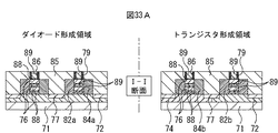
続いて、図33A〜図33Cに示すように、ゲート電極89を形成する。図33Cが平面図であり、図33Aが図33C中の破線I−Iに沿った断面図、図33Bが図33C中の破線II−IIに沿った断面図である。
詳細には、空隙87を埋め込むように、層間絶縁膜85上に電極材料として例えば多結晶シリコン膜を堆積する。CMP法により、多結晶シリコン膜を、層間絶縁膜85の表面が露出するまで平坦化する。以上により、空隙87を充填してSi層76とゲート絶縁膜88を介して対向するゲート電極89が形成される。なお、多結晶シリコン膜でゲート電極89を形成する代わりに、ゲート電極の材料として窒化チタンや窒化タンタル等を形成するようにしても良い。Subsequently, as shown in FIGS. 33A to 33C, the
Specifically, for example, a polycrystalline silicon film is deposited as an electrode material on the
続いて、図34に示すように、コンタクトプラグ92a,92bを形成する。
詳細には、先ず、層間絶縁膜85上に絶縁膜、例えばシリコン酸化膜をCVD法等により堆積し、層間絶縁膜91を形成する。
次に、リソグラフィー及びドライエッチングにより、層間絶縁膜85,91を加工する。これにより、ダイオード形成領域では、層間絶縁膜85,91にp型領域84a及びn型領域82aの表面の一部を露出する開口が形成される。トランジスタ形成領域では、層間絶縁膜85,91にp型ソース/ドレイン領域84b及びn型ソース/ドレイン領域82bの表面の一部を露出する開口と、層間絶縁膜91にゲート電極89の表面の一部を露出する開口とが形成される。
次に、各開口を埋め込むように、層間絶縁膜91上に金属材料、例えばチタン又は窒化チタンを下地とするタングステンを堆積する。CMP法により、堆積されたチタン又は窒化チタン及びタングステンを層間絶縁膜91の上面が露出するまで平坦化する。以上により、ダイオード形成領域では、p型領域84a及びn型領域82aとそれぞれ接続されたコンタクトプラグ92aが形成される。トランジスタ形成領域では、p型ソース/ドレイ領域84b及びn型ソース/ドレイン領域82bとそれぞれ接続されたコンタクトプラグ92aと、ゲート電極89と接続されたコンタクトプラグ92bとが形成される。Subsequently, as shown in FIG. 34, contact plugs 92a and 92b are formed.
Specifically, first, an insulating film, for example, a silicon oxide film is deposited on the
Next, the
Next, a metal material, for example, tungsten based on titanium or titanium nitride is deposited on the
続いて、第1の実施形態と同様に、第1配線層を形成する。ダイオード形成領域において、第1配線層を構成する配線93,94を図35に示す。図35では、層間絶縁膜85,91等の図示を省略する。
配線93,94は、縦方向に並ぶ複数のゲート電極89の上方で延在する部分と、p型領域84a上のコンタクトプラグ92a又はn型領域82a上のコンタクトプラグ92aと接続する部分とが一体形成されて構成されている。Subsequently, as in the first embodiment, a first wiring layer is formed. In the diode formation region, the
The
しかる後、第1の実施形態と同様に、第1配線層を含む多層配線構造及び接続パッドを形成し、本実施形態による半導体装置とされる。接続パッドは、ダイオード形成領域及びトランジスタ形成領域の上方に、平面視でダイオード形成領域及びトランジスタ形成領域を内包するように配される。 Then, similarly to the first embodiment, the multilayer wiring structure including the first wiring layer and the connection pad are formed to complete the semiconductor device according to the present embodiment. The connection pad is arranged above the diode formation region and the transistor formation region so as to include the diode formation region and the transistor formation region in plan view.
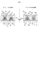
本実施形態では、ダイオード形成領域には、図34のように、ESD保護ダイオードとして、第1のダイオードDA及び第2のダイオードDBが形成され、両者が並列に接続されている。トランジスタ形成領域には、図34のように、PMOSトランジスタ及びNMOSトランジスタが形成されている。In the present embodiment, as shown in FIG. 34, a first diode D A and a second diode D B are formed as ESD protection diodes in the diode formation region, and both are connected in parallel. As shown in FIG. 34, PMOS transistors and NMOS transistors are formed in the transistor formation region.
第1のダイオードDAは、ゲート電極89を有し、ゲート電極89の近傍におけるSi層76に電流経路が形成されるゲート型ダイオードである。第2のダイオードDBは、STI素子分離構造77を有し、STI素子分離構造77の近傍におけるp型ウェル72に電流経路が形成されるSTI型ダイオードである。
The first diode D A is a gate type diode having a
図36Aは、本実施形態における半導体装置のダイオード形成領域のレイアウト構成を示す概略平面図である。図36Bは、図36A中の破線I−Iに沿った概略断面図である。
ダイオード形成領域では、複数のゲート電極89が行列状に配列しており、横方向及び縦方向の各々について、2つのp型領域84a及び2つのn型領域82aが交互に、言わば市松模様状に配置されている。FIG. 36A is a schematic plan view showing the layout configuration of the diode formation region of the semiconductor device in the present embodiment. FIG. 36B is a schematic sectional view taken along the broken line I-I in FIG. 36A.
In the diode formation region, a plurality of
第1のダイオードDAと第2のダイオードDBとでは、p型領域84a及びn型領域82aを共有している。第1のダイオードDAは、横方向に配列しており、ゲート電極89とその両側のp型領域84a及びn型領域82aとを有して構成される。第2のダイオードDBは、横方向及び縦方向に配列しており、p型領域84a及びn型領域82aと、これらの間のSTI素子分離構造77とを有して構成される。The first diode D A and the second diode D B share the p-
本実施形態の半導体装置では、ダイオード形成領域において、上記のように、横方向にはゲート型ダイオードである複数の第1のダイオードDAが、横方向及び縦方向にはSTI型ダイオードである複数の第2のダイオードDBが形成されている。第1のダイオードDA及び第2のダイオードDBは並列に接続されている。この構成により、第1の実施形態の図13と同様に、サージ電流が生じた場合には、2種類の電流経路が形成される。そのため、従来技術のように、ESD保護ダイオードがゲート型ダイオードのみ又はSTI型ダイオードのみの場合と比較して電流経路が増加し、ESD保護ダイオードの低抵抗化が実現する。また、本実施形態のように、p型領域84a及びn型領域82aを交互に配置することにより、従来技術の場合と比較して、ESD保護ダイオードの占有面積を低減させることができる。In the semiconductor device of the present embodiment, in the diode formation region, as described above, the plurality of first diodes D A which are gate type diodes in the lateral direction and the plurality of STI type diodes which are the lateral direction and the vertical direction are provided. Second diode D B is formed. The first diode D A and the second diode D B are connected in parallel. With this configuration, similarly to FIG. 13 of the first embodiment, two types of current paths are formed when a surge current occurs. Therefore, as in the prior art, the current path is increased as compared with the case where the ESD protection diode is only the gate type diode or the STI type diode, and the resistance of the ESD protection diode is reduced. Further, by alternately disposing the p-
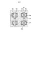
本実施形態における半導体装置のダイオード形成領域のレイアウトとしては、図36Aのレイアウトに代えて、例えば図37のように構成しても良い。図37では、隣接する2つのp型領域84a及び隣接する2つのn型領域82aをそれぞれ接続して一体形成している。この構成により、STI型ダイオードである第2のダイオードの領域が増加し、更なる低抵抗化が実現する。また、p型領域84a及びn型領域82aの面積が増加するため、コンタクトプラグの接続が容易となる。
The layout of the diode formation region of the semiconductor device in this embodiment may be configured as shown in FIG. 37, for example, instead of the layout in FIG. 36A. In FIG. 37, two adjacent p-
また、本実施形態における半導体装置のダイオード形成領域のレイアウトとしては、例えば図38のように構成しても良い。図38では、横方向について、・・・p型領域84a、ゲート電極89、n型領域82a、ゲート電極89・・・のように隣接して形成されている。横方向にはゲート型ダイオードである複数の第1のダイオードDAが、縦方向にはSTI型ダイオードである複数の第2のダイオードDBが形成されている。この構成により、複数のゲート電極89を等間隔且つ高密度で配設することができる。The layout of the diode formation region of the semiconductor device in this embodiment may be configured as shown in FIG. 38, for example. In FIG. 38, the p-
以上説明したように、本実施形態によれば、低抵抗化及び占有面積の低減を図るも、大きなサージ電流に十分に対処することができるESD保護ダイオードを備えた信頼性の高い半導体装置が実現する。 As described above, according to the present embodiment, it is possible to realize a highly reliable semiconductor device including an ESD protection diode that can sufficiently cope with a large surge current while achieving a reduction in resistance and a reduction in occupied area. To do.
なお、上記実施形態は、何れも本発明を実施するにあたっての具体化の例を示したものに過ぎず、これらによって本発明の技術的範囲が限定的に解釈されてはならないものである。すなわち、本発明はその技術思想、又はその主要な特徴から逸脱することなく、様々な形で実施することができる。 It should be noted that each of the above-described embodiments is merely an example of an embodiment for carrying out the present invention, and the technical scope of the present invention should not be limitedly interpreted by these. That is, the present invention can be implemented in various forms without departing from the technical idea or the main features thereof.
半導体装置の一態様は、ESD保護ダイオードを備えた信頼性の高い半導体装置であり、ESD保護ダイオードの低抵抗化及び占有面積の低減を図るも、大きなサージ電流が生じても静電破壊を確実に防止することができる。 One mode of a semiconductor device is a highly reliable semiconductor device including an ESD protection diode. Although the resistance of the ESD protection diode is reduced and the occupied area is reduced, electrostatic breakdown is ensured even when a large surge current occurs. Can be prevented.
Claims (14)
ゲートと、
前記ゲート及び半導体層に接する第1の絶縁体と、
前記半導体層に形成された第2の絶縁体と、
前記第1の絶縁体に接する前記半導体層の部分を電流経路に有する複数の第1のダイオードと、
前記第2の絶縁体に接する前記半導体層の部分を電流経路に有する複数の第2のダイオードと、
を備えており、
複数の前記第1のダイオードが第1の方向に配列し、
複数の前記第2のダイオードが前記第1の方向と異なる第2の方向に配列し、
前記第1のダイオードと前記第2のダイオードとが並列に接続されていることを特徴とする半導体装置。 A semiconductor layer,
The gate,
A first insulator in contact with the gate and the semiconductor layer,
A second insulator formed on the semiconductor layer;
A plurality of first diodes having a portion of the semiconductor layer in contact with the first insulator in a current path;
A plurality of second diodes each having a portion of the semiconductor layer in contact with the second insulator in a current path;
Is equipped with
A plurality of the first diodes are arranged in a first direction,
A plurality of the second diodes are arranged in a second direction different from the first direction,
A semiconductor device, wherein the first diode and the second diode are connected in parallel.
ゲートと、
前記ゲート及び半導体層に接する第1の絶縁体と、
前記半導体層に形成された第2の絶縁体と、
前記第1の絶縁体に接する前記半導体層の部分を電流経路に有する複数の第1のダイオードと、
前記第2の絶縁体に接する前記半導体層の部分を電流経路に有する複数の第2のダイオードと、
を備えており、
複数の前記第1のダイオードが第1の方向に配列し、
複数の前記第2のダイオードが前記第1の方向及び前記第1の方向と異なる第2の方向に配列し、
前記第1のダイオードと前記第2のダイオードとが並列に接続されていることを特徴とする半導体装置。 A semiconductor layer,
The gate,
A first insulator in contact with the gate and the semiconductor layer,
A second insulator formed on the semiconductor layer;
A plurality of first diodes having a portion of the semiconductor layer in contact with the first insulator in a current path;
A plurality of second diodes each having a portion of the semiconductor layer in contact with the second insulator in a current path;
Is equipped with
A plurality of the first diodes are arranged in a first direction,
A plurality of the second diodes are arranged in the first direction and a second direction different from the first direction,
A semiconductor device, wherein the first diode and the second diode are connected in parallel.
前記第1のフィンに形成された第1導電型の第1領域と、
前記第1のフィンに形成された前記第1導電型とは異なる第2導電型の第2領域と、
前記第2のフィンに形成された前記第2導電型の第3領域と、
を有し、
前記複数の第1のダイオードの一は、前記第1領域及び前記第2領域を有し、
前記複数の第2のダイオードの一は、前記第1領域及び前記第3領域を有することを特徴とする請求項1に記載の半導体装置。 The semiconductor layer has a first fin and a second fin that extend in the first direction and are arranged side by side in the second direction,
A first region of a first conductivity type formed on the first fin;
A second region of a second conductivity type different from the first conductivity type formed in the first fin;
A third region of the second conductivity type formed on the second fin;
Have
One of the plurality of first diodes has the first region and the second region,
The semiconductor device according to claim 1, wherein one of the plurality of second diodes has the first region and the third region.
前記複数の第1のダイオードの一は、前記第3領域及び前記第4領域を有し、
前記複数の第2のダイオードの一は、前記第2領域及び前記第4領域を有することを特徴とする請求項3に記載の半導体装置。 A fourth region of the first conductivity type formed in the second fin,
One of the plurality of first diodes has the third region and the fourth region,
The semiconductor device according to claim 3, wherein one of the plurality of second diodes has the second region and the fourth region.
前記第2のフィンに形成された複数の前記第3領域及び複数の前記第4領域と、を有し、
前記第1のフィンでは、前記第1領域と前記第2領域とが前記第1の方向に交互に配置され、
前記第2のフィンでは、前記第3領域と前記第4領域とが前記第1の方向に交互に配置されることを特徴とする請求項4に記載の半導体装置。 A plurality of the first regions and a plurality of the second regions formed on the first fin;
A plurality of the third regions and a plurality of the fourth regions formed in the second fin,
In the first fin, the first region and the second region are alternately arranged in the first direction,
The semiconductor device according to claim 4, wherein in the second fin, the third region and the fourth region are alternately arranged in the first direction.
複数の前記第2のフィンを有し、前記第2の方向で前記第1の群と並んで配置される第2の群と、
を有することを特徴とする請求項3〜5のいずれか1項に記載の半導体装置。 A first group having a plurality of the first fins;
A second group having a plurality of the second fins and arranged side by side with the first group in the second direction;
The semiconductor device according to any one of claims 3 to 5, further comprising:
前記ウェルが前記第2のダイオードの電流経路の一部であることを特徴とする請求項3〜6のいずれか1項に記載の半導体装置。 Wherein formed on the semiconductor layer, a portion is positioned below the second insulator has a well having any conductivity type of said first conductivity type and said second conductivity type,
The semiconductor device according to any one of claims 3-6, wherein the well is part of the current path of said second diode.
前記第1のダイオード及び前記第2のダイオード上に形成され、前記第2領域及び前記第3領域を電気的に接続し、それぞれ前記第2の方向に延在する複数の第2の配線と、
を有することを特徴とする請求項4又は5に記載の半導体装置。 A plurality of first wirings formed on the first diode and the second diode, electrically connecting the first region and the fourth region, each extending in the second direction;
A plurality of second wirings formed on the first diode and the second diode, electrically connecting the second region and the third region, each extending in the second direction;
The semiconductor device according to claim 4, further comprising:
前記第1のダイオードは、前記ワイヤ状部分を電流経路として有することを特徴とする請求項1又は2に記載の半導体装置。 The semiconductor layer has a wire-shaped portion,
The semiconductor device according to claim 1, wherein the first diode has the wire-shaped portion as a current path.
前記第1の方向及び前記第2の方向の各々について、前記第1導電型の領域及び前記第2導電型の領域が交互に配置されていることを特徴とする請求項1,2,9のいずれか1項に記載の半導体装置。 The first diode and the second diode share a first conductivity type region and a second conductivity type region different from the first conductivity type,
10. The regions of the first conductivity type and the regions of the second conductivity type are alternately arranged for each of the first direction and the second direction. The semiconductor device according to claim 1.
ゲートと、
前記ゲート及び半導体層に接する第1の絶縁体と、
前記半導体層に形成された第2の絶縁体と、
前記第1の絶縁体に接する前記半導体層の部分を電流経路に有する複数の第1のダイオードと、
前記第2の絶縁体に接する前記半導体層の部分を電流経路に有する複数の第2のダイオードと、
第1導電型の第1領域と、
前記第1領域の上方に位置し、前記第1導電型とは異なる第2導電型の第2領域と、
前記第2導電型の第3領域と、
前記第3領域の上方に位置し、前記第1導電型の第4領域と、を有し、
複数の前記第1のダイオードの一は、前記第1領域及び前記第2領域を有し、
複数の前記第1のダイオードの別の一は、前記第3領域及び前記第4領域を有し、
前記第2のダイオードは、前記第1領域及び前記第3領域を有し、
前記第1のダイオードと前記第2のダイオードとが並列に接続することを特徴とする半導体装置。 A semiconductor layer,
The gate,
A first insulator in contact with the gate and the semiconductor layer,
A second insulator formed on the semiconductor layer;
A plurality of first diodes having a portion of the semiconductor layer in contact with the first insulator in a current path;
A plurality of second diodes each having a portion of the semiconductor layer in contact with the second insulator in a current path;
A first region of a first conductivity type;
A second region located above the first region and having a second conductivity type different from the first conductivity type;
A third region of the second conductivity type,
Located above the third region and having a fourth region of the first conductivity type,
One of a plurality of said first diode has a first region and the second region,
Another of the plurality of the first diode has the third region and the fourth region,
The second diode has the first region and the third region,
A semiconductor device, wherein the first diode and the second diode are connected in parallel.
前記ダイオード形成領域及び前記トランジスタ形成領域の上方に接続パッドが設けられており、前記ダイオード形成領域及び前記トランジスタ形成領域は、平面視で前記接続パッドに内包されていることを特徴とする請求項1〜13のいずれか1項に記載の半導体装置。 A diode forming region in which the first diode and the second diode are formed, and a transistor forming region in which a transistor is formed,
The connection pad is provided above the diode formation region and the transistor formation region, and the diode formation region and the transistor formation region are included in the connection pad in a plan view. The semiconductor device according to claim 1.
Applications Claiming Priority (1)
| Application Number | Priority Date | Filing Date | Title |
|---|---|---|---|
| PCT/JP2016/067384 WO2017212644A1 (en) | 2016-06-10 | 2016-06-10 | Semiconductor device |
Publications (2)
| Publication Number | Publication Date |
|---|---|
| JPWO2017212644A1 JPWO2017212644A1 (en) | 2019-04-11 |
| JP6700565B2 true JP6700565B2 (en) | 2020-05-27 |
Family
ID=60578190
Family Applications (1)
| Application Number | Title | Priority Date | Filing Date |
|---|---|---|---|
| JP2018522287A Active JP6700565B2 (en) | 2016-06-10 | 2016-06-10 | Semiconductor device |
Country Status (4)
| Country | Link |
|---|---|
| US (1) | US20190081032A1 (en) |
| JP (1) | JP6700565B2 (en) |
| CN (1) | CN109219874A (en) |
| WO (1) | WO2017212644A1 (en) |
Families Citing this family (8)
| Publication number | Priority date | Publication date | Assignee | Title |
|---|---|---|---|---|
| CN108878541B (en) * | 2017-05-08 | 2021-07-02 | 中芯国际集成电路制造(上海)有限公司 | Fin type diode and manufacturing method thereof |
| WO2020235084A1 (en) * | 2019-05-23 | 2020-11-26 | 株式会社ソシオネクスト | Semiconductor device |
| CN113841228A (en) * | 2019-05-23 | 2021-12-24 | 株式会社索思未来 | Semiconductor device with a plurality of semiconductor chips |
| US20220102385A1 (en) * | 2020-09-25 | 2022-03-31 | Intel Corporation | Substrate-free integrated circuit structures |
| US20220416022A1 (en) * | 2021-06-24 | 2022-12-29 | Intel Corporation | Substrate-less nanowire-based lateral diode integrated circuit structures |
| US11764207B2 (en) * | 2021-09-22 | 2023-09-19 | Samsung Electronics Co., Ltd. | Diode structures of stacked devices and methods of forming the same |
| WO2023167083A1 (en) * | 2022-03-02 | 2023-09-07 | 株式会社ソシオネクスト | Semiconductor integrated circuit device |
| CN117334693B (en) * | 2023-10-12 | 2024-05-07 | 北京大学 | Semiconductor preparation method, semiconductor structure and chip |
Family Cites Families (16)
| Publication number | Priority date | Publication date | Assignee | Title |
|---|---|---|---|---|
| US5754380A (en) * | 1995-04-06 | 1998-05-19 | Industrial Technology Research Institute | CMOS output buffer with enhanced high ESD protection capability |
| WO2000077859A1 (en) * | 1999-06-16 | 2000-12-21 | Matsushita Electric Industrial Co., Ltd. | Semiconductor device |
| JP3727220B2 (en) * | 2000-04-03 | 2005-12-14 | Necエレクトロニクス株式会社 | Semiconductor device |
| US20010043449A1 (en) * | 2000-05-15 | 2001-11-22 | Nec Corporation | ESD protection apparatus and method for fabricating the same |
| EP1402574A2 (en) * | 2001-07-05 | 2004-03-31 | Sarnoff Corporation | Electrostatic discharge (esd) protection device with simultaneous and distributed self-biasing for multi-finger turn-on |
| JP2009071173A (en) * | 2007-09-14 | 2009-04-02 | Panasonic Corp | Semiconductor device |
| US8461651B2 (en) * | 2010-11-04 | 2013-06-11 | Shanghai Institute Of Microsystem And Information Technology, Chinese Academy Of Sciences | ESD protection devices for SOI integrated circuit and manufacturing method thereof |
| US9236372B2 (en) * | 2011-07-29 | 2016-01-12 | Freescale Semiconductor, Inc. | Combined output buffer and ESD diode device |
| JP5281215B1 (en) * | 2011-09-08 | 2013-09-04 | ユニサンティス エレクトロニクス シンガポール プライベート リミテッド | Solid-state imaging device |
| US8941181B2 (en) * | 2011-12-08 | 2015-01-27 | Texas Instruments Incorporated | Compensated well ESD diodes with reduced capacitance |
| KR101979637B1 (en) * | 2012-11-26 | 2019-08-28 | 삼성전자주식회사 | Semiconductor device |
| US10665709B2 (en) * | 2013-09-10 | 2020-05-26 | Delta Electronics, Inc. | Power semiconductor device integrated with ESD protection circuit under source pad, drain pad, and/or gate pad |
| US9147676B2 (en) * | 2013-10-02 | 2015-09-29 | Taiwan Semiconductor Manufacturing Company, Ltd. | SCRs with checker board layouts |
| US9368500B2 (en) * | 2013-11-05 | 2016-06-14 | United Microelectronics Corp. | Complementary metal-oxide-semiconductor device |
| US9461170B2 (en) * | 2014-04-23 | 2016-10-04 | Taiwan Semiconductor Manufacturing Company Ltd. | FinFET with ESD protection |
| US9653448B2 (en) * | 2014-07-17 | 2017-05-16 | Apple Inc. | Electrostatic discharge (ESD) diode in FinFET technology |
-
2016
- 2016-06-10 JP JP2018522287A patent/JP6700565B2/en active Active
- 2016-06-10 WO PCT/JP2016/067384 patent/WO2017212644A1/en active Application Filing
- 2016-06-10 CN CN201680086234.XA patent/CN109219874A/en active Pending
-
2018
- 2018-11-08 US US16/184,695 patent/US20190081032A1/en not_active Abandoned
Also Published As
| Publication number | Publication date |
|---|---|
| CN109219874A (en) | 2019-01-15 |
| JPWO2017212644A1 (en) | 2019-04-11 |
| US20190081032A1 (en) | 2019-03-14 |
| WO2017212644A1 (en) | 2017-12-14 |
Similar Documents
| Publication | Publication Date | Title |
|---|---|---|
| JP6700565B2 (en) | Semiconductor device | |
| US10658293B2 (en) | Semiconductor device having a multilayer wiring structure | |
| TWI677922B (en) | Methods of forming gate contact structures and cross-coupled contact structures for transistor devices | |
| JP4875622B2 (en) | Manufacturing method of semiconductor device | |
| TWI646646B (en) | Semiconductor component and method of manufacturing same | |
| CN102820280B (en) | For the overstepping one's bounds laminar metal level of integrated circuit | |
| TWI645510B (en) | Methods of forming a high-k contact liner to improve effective via separation distance and the resulting devices | |
| CN106941091B (en) | Interconnect structure, interconnect layout structure and method for fabricating the same | |
| TWI438901B (en) | Power semiconductor device having low gate input resistance and manufacturing method thereof | |
| US20210184035A1 (en) | Semiconductor device and manufacturing method thereof | |
| KR102460719B1 (en) | Semiconductor device and method of fabricating the same | |
| KR20180103397A (en) | Integrated circuit device | |
| US20040089915A1 (en) | Semiconductor device with fuses | |
| JP2006344773A (en) | Semiconductor device and its manufacturing method | |
| JP4744103B2 (en) | Semiconductor device including resistance element and manufacturing method thereof | |
| JP6160360B2 (en) | Electronic device and manufacturing method thereof | |
| JP2008041835A (en) | Semiconductor device, and manufacturing method thereof | |
| US9852950B2 (en) | Superimposed transistors with auto-aligned active zone of the upper transistor | |
| KR102516407B1 (en) | Three-dimensional stacked semiconductor device and its manufacturing method | |
| JP2009071283A (en) | Semiconductor device | |
| JP2014011165A (en) | Semiconductor device manufacturing method | |
| JP2010080725A (en) | Semiconductor device | |
| JP2013105988A (en) | Method of manufacturing semiconductor device, and semiconductor device | |
| JP2004363254A (en) | Semiconductor device and its fabricating process | |
| KR20120097713A (en) | Method for fabricating semiconductor device |
Legal Events
| Date | Code | Title | Description |
|---|---|---|---|
| A524 | Written submission of copy of amendment under section 19 (pct) |
Free format text: JAPANESE INTERMEDIATE CODE: A527 Effective date: 20180717 |
|
| A621 | Written request for application examination |
Free format text: JAPANESE INTERMEDIATE CODE: A621 Effective date: 20190522 |
|
| A131 | Notification of reasons for refusal |
Free format text: JAPANESE INTERMEDIATE CODE: A131 Effective date: 20200114 |
|
| A521 | Written amendment |
Free format text: JAPANESE INTERMEDIATE CODE: A523 Effective date: 20200313 |
|
| TRDD | Decision of grant or rejection written | ||
| A01 | Written decision to grant a patent or to grant a registration (utility model) |
Free format text: JAPANESE INTERMEDIATE CODE: A01 Effective date: 20200331 |
|
| A61 | First payment of annual fees (during grant procedure) |
Free format text: JAPANESE INTERMEDIATE CODE: A61 Effective date: 20200413 |
|
| R150 | Certificate of patent or registration of utility model |
Ref document number: 6700565 Country of ref document: JP Free format text: JAPANESE INTERMEDIATE CODE: R150 |