JP2004363254A - Semiconductor device and its fabricating process - Google Patents
Semiconductor device and its fabricating process Download PDFInfo
- Publication number
- JP2004363254A JP2004363254A JP2003158478A JP2003158478A JP2004363254A JP 2004363254 A JP2004363254 A JP 2004363254A JP 2003158478 A JP2003158478 A JP 2003158478A JP 2003158478 A JP2003158478 A JP 2003158478A JP 2004363254 A JP2004363254 A JP 2004363254A
- Authority
- JP
- Japan
- Prior art keywords
- wiring
- semiconductor device
- gate electrode
- dummy wiring
- insulating film
- Prior art date
- Legal status (The legal status is an assumption and is not a legal conclusion. Google has not performed a legal analysis and makes no representation as to the accuracy of the status listed.)
- Pending
Links
Images


Abstract
Description
【0001】
【発明の属する技術分野】
本発明は、半導体装置及びその製造方法に関する。
【0002】
【従来の技術】
近年、半導体集積回路によって構成された半導体装置においては、高集積化が大きく進展してきている。特に、MIS( Metal Insulated semiconductor )型の半導体装置においては、高集積化に対応するため、トランジスタ等の素子の微細化、高性能化が図られており、更なる微細化、高性能化も求められている。
【0003】
また、このような半導体装置の配線の形成工程においては、プラズマCVDやプラズマエッチングに代表されるプラズマプロセスの利用が増加している。これは、半導体装置の配線の形成工程においては、不純物の拡散の点や金属配線材料の耐熱性の点から熱処理量に制約があり、プラズマプロセスによれば熱処理量を小さくできるからである。
【0004】
更に、近年においては、高性能化を図るため銅(Cu)配線が導入される場合があるが、銅(Cu)配線の形成にはダマシン法が使用されるため、この場合は、益々、プラズマプロセスの利用が増大する。
【0005】
このように、プラズマプロセスはエッチング時だけでなく、成膜時にも多用されており、プラズマプロセスの利用は年々増加傾向にある。ところが、プラズマプロセスの利用増大に伴い、プラズマプロセスによるデバイス損傷が顕在化してきている。これを主に「プラズマチャージングダメージ」と呼び、近年大きくクローズアップされている。
【0006】
このようなプラズマチャージングダメージを受けた半導体装置においては、デバイス特性が劣化するため、不良品となる。また、プラズマチャージングダメージの問題においては、特に、ゲート絶縁膜における信頼性の劣化が重大な問題となっている。
【0007】
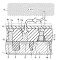
ここで、プラズマチャージングダメージについて図6及び図7を用いて説明する。図6は、従来の半導体装置の構成を部分的に示す断面図であり、図6(a)は半導体装置を構成する半導体基板の法線方向に沿って切断した断面図、図6(b)は図6(a)に示す切断線C−C´に沿って切断した断面図である。
【0008】
図6(a)に示すように、従来の半導体装置は、n型シリコン基板21を備えている。シリコン基板21には、STI(Shallow Trench Isolation)法によって、複数の素子分離22が、所定の間隔をおいて、シリコン基板21上に露出するように形成されている。
【0009】
シリコン基板21上の素子分離22間には、シリコン基板21の内部に形成されたpウェル(p well)23と、ゲート絶縁膜(膜厚2.2nm)26と、n+ポリシリコンで形成されたゲート電極27と、シリコン基板21の表層部分に設けられたソース(n+)領域24a及びドレイン(n+)領域24bとによって、nチャンネルMOSトランジスタが形成されている。
【0010】
ゲート絶縁膜26及びゲート電極27は、互いに整合されるように形成されており、これらの両側面には、両側面を覆うようにサイドウォール28が形成されている。なお、35は、n+領域であって、他のトランジスタのソース領域又はドレイン領域として機能する活性領域である。
【0011】
また、シリコン基板21の上には、多層配線を実現するための下地層間絶縁膜30と層間絶縁膜32とが順に積層されている。下地層間絶縁膜30には、配線31a〜31cが形成されている。配線31a〜31cは、ダマシン法によって形成された銅配線(厚み500nm)であり、下地層間絶縁膜30に埋め込まれている。
【0012】
配線31aは、Wプラグ29bを介してゲート電極27に接続されるゲート電極接続用配線である。また、配線31cは、Wプラグ29aを介してn+領域25に接続されるソース・ドレイン接続用配線である。配線31a及び31cは、図6(b)に示すように短冊状に形成されている。
【0013】
Wプラグ29a及び29bは、下地層間絶縁膜30に形成されたコンタクトホールに、タングステンを充填して形成されている。なお、Wプラグ29aはn+領域25に接続するように形成されており、Wプラグ29bはゲート電極27に接続するように形成されている。
【0014】
配線31bは、ダマシン法で実施されるCMP(chemical mechanical polishing)工程における平坦性の確保のためのダミー配線であり、配線31aに隣接して形成されている。配線31bは、図6(b)に示すように、複数個で構成されており、正方形状に形成されている。また、配線31bは、その全周囲が下地層間絶縁膜30と層間絶縁膜32とによって絶縁されており、電気的に浮遊した状態にある。
【0015】
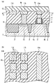
図7は、図6に示す従来の半導体装置における層間絶縁膜の形成工程を示す断面図であり、プラズマチャージングダメージの発生を概念的に示している。
【0016】
最初に、素子分離22とpウェル23とが設けられたシリコン基板21上に、ゲート絶縁膜26を形成する。次に、ゲート絶縁膜26の上にゲート電極27を形成し、ゲート絶縁膜26及びゲート電極27の両側面にサイドウォール28を形成する。次いで、イオン注入によって、n+領域25、ソース(n+)領域24a及びドレイン(n+)領域24bを形成して、下地層間絶縁膜30を成膜する。
【0017】
次に、下地層間絶縁膜30にWプラグ29a及び29bを形成した後、ダマシン法を用いて配線31a〜31cを同時に形成する。具体的には、下地層間絶縁膜30における配線31a〜31cを設けるべき位置に溝を形成し、この溝が埋まるように銅の層を形成した後、CMP法によって余分な厚みを研磨によって除去する。
【0018】
次に、図7に示すように、プラズマCVD装置(図示せず)によってプラズマ33を発生させて、層間絶縁膜32の成膜を行う。この場合、配線31bは、上述したように電気的に浮遊しており、又配線31cはシリコン基板21に直接接続されているため、プラズマ33からのチャージング電流はゲート電極27及びゲート絶縁膜26へと流れることになる。このため、ゲート絶縁膜26が破壊され、デバイス特性が劣化してしまう。
【0019】
このような問題を解決するため、特許文献1には、半導体基板上に、ゲート電極に接続された保護ダイオードを設けた半導体装置が開示されている。特許文献1に開示された半導体装置においては、プラズマチャージングダメージを生じさせるチャージング電流は保護ダイオードを介して設置電位に逃がされる。このため、チャージング電流がゲート絶縁膜に印加されるのが抑制され、ゲート絶縁膜の破壊が回避される。
【0020】
【特許文献1】
特開平10−173157号公報(第20段落、第2図−第9図)
【0021】
【発明が解決しようとする課題】
しかしながら、半導体装置の高集積化により、ゲート絶縁膜は、年々、薄膜化しており、この結果、ゲート絶縁膜の絶縁耐圧は、保護ダイオードの接合耐圧に比べて小さくなってきている。このため、ゲート絶縁膜の薄膜化が進行するにつれ、保護ダイオードに流れないで、ゲート電極へとリークするチャージング電流が増大している。
【0022】
このことから、保護ダイオードによるプラズマチャージングダメージの抑制効果は、ゲート絶縁膜の薄膜化に伴って小さなものとなっており、保護ダイオードを設けているにも拘わらず、プラズマチャージングダメージによるデバイス特性の劣化が生じている。
【0023】
本発明の目的は、上記問題を解決し、プラズマプロセスにおけるプラズマチャージングダメージの抑制を図り得る半導体装置及びその製造方法を提供することにある。
【0024】
【課題を解決するための手段】
上記目的を達成するために本発明にかかる半導体装置は、半導体基板と、前記半導体基板上に設けられたゲート絶縁膜と、前記ゲート絶縁膜の上に設けられたゲート電極と、前記ゲート絶縁膜及び前記ゲート電極を被覆する絶縁層と、前記絶縁層に設けられた配線とを有する半導体装置であって、前記配線は、前記ゲート電極に電気的に接続されたゲート電極用配線と、ダミー配線とを有し、前記ダミー配線は、前記半導体基板に形成された活性領域に電気的に接続されていることを特徴とする。
【0025】
上記本発明にかかる半導体装置によれば、ダミー配線がシリコン基板に形成された活性領域に電気的に接続されている。このため、プラズマによるチャージング電流は、ゲート電極用配線ではなく、ダミー配線へと流れることとなる。また、ダミー配線は、従来技術における特許文献1に開示された保護ダイオードではなく、活性領域に電気的接続されている。このため、本発明にかかる半導体装置によれば、ゲート絶縁膜の薄膜化が更に進んだとしても、チャージング電流がゲート電極用配線へとリークするのを抑制できる。
【0026】
上記本発明にかかる半導体装置においては、前記ダミー配線が接続された活性領域が、ソース領域及びドレイン領域のいずれとしても機能しない活性領域であるのが好ましい。この場合、前記半導体基板に、ソース領域又はドレイン領域として機能する活性領域が形成されており、前記配線が、前記ソース領域又はドレイン領域として機能する活性領域に電気的に接続された配線を更に有しているのが好ましい。
【0027】
また、上記本発明にかかる半導体装置においては、前記配線が第2のダミー配線を更に有し、前記第2のダミー配線は、前記ダミー配線と隣接する位置に形成されており、前記第2のダミー配線の全周囲は前記絶縁層によって絶縁されているのが好ましい。この場合、前記ダミー配線が前記ゲート電極用配線に隣接する位置に配置されており、前記第2のダミー配線が複数の配線で構成され、前記第2のダミー配線を構成する複数の配線が、前記ダミー配線の前記ゲート電極用配線に隣接していない側において、前記ダミー配線を囲むように配置されているのが好ましい。
【0028】
更に、上記本発明にかかる半導体装置においては、前記配線が、ダマシン法によって形成されたものであって、前記絶縁層に埋め込まれており、前記ダミー配線が接続された活性領域が、前記ゲート絶縁膜が設けられた前記半導体基板の領域に隣接した位置に、素子分離を隔てて設けられているのが好ましい。
【0029】
また、前記ゲート電極用配線、前記ダミー配線、および前記第2のダミー配線は、同一の金属材料によって形成されているのが好ましく、前記金属材料としては銅を含む金属材料が挙げられる。
【0030】
次に、上記目的を達成するために本発明にかかる半導体装置の製造方法は、(a)半導体基板上に、ゲート絶縁膜及びゲート電極の積層体と、活性領域とを少なくとも形成する工程と、(b)前記半導体基板上に、前記積層体及び前記活性領域を被覆する第1の絶縁層を形成する工程と、(c)前記第1の絶縁層に、前記ゲート電極に電気的に接続されるゲート電極用配線と、前記活性領域に電気的に接続されるダミー配線とを同時に設ける工程と、(d)前記第1の絶縁層の上に、プラズマプロセスによって、第2の絶縁層を形成する工程とを有することを特徴とする。
【0031】
上記本発明にかかる半導体装置の製造方法によれば、シリコン基板に形成された活性領域にダミー配線を電気的に接続した状態で、第2の絶縁層の成膜を行っている。このため、プラズマによって第2の絶縁層の成膜時に発生するチャージング電流は、ゲート電極用配線ではなく、ダミー配線へと流れることとなる。また、ダミー配線は、従来技術における特許文献1に開示された保護ダイオードではなく、活性領域に電気的接続されている。このため、本発明にかかる半導体装置の製造方法によれば、ゲート絶縁膜の薄膜化が更に進んだとしても、チャージング電流がゲート電極用配線へとリークするのを抑制できる。
【0032】
上記本発明にかかる半導体装置の製造方法においては、前記(d)の工程において、前記プラズマプロセスによって発生したプラズマからのチャージング電流を、前記ダミー配線によって排出しながら、前記第2の絶縁層を形成するのが好ましい。また、前記(c)の工程において、前記ゲート電極用配線と前記ダミー配線とをダマシン法によって形成するのも好ましい。
【0033】
また、上記本発明にかかる半導体装置の製造方法においては、前記(a)の工程において、ソース領域又はドレイン領域として機能する活性領域と、ソース領域及びドレイン領域のいずれとしても機能しない活性領域とを形成し、前記(c)の工程において、前記ソース領域及びドレイン領域のいずれとしても機能しない活性領域に前記ダミー配線を接続するのが好ましい。更に、前記第1の絶縁層が多層配線を形成するための下地層間絶縁膜であり、前記第2の絶縁層が多層配線を形成するための層間絶縁膜であるのが好ましい。
【0034】
更に、上記本発明にかかる半導体装置の製造方法においては、前記(c)の工程において、前記ダミー配線と隣接する位置に、前記第1の絶縁層によって前記ゲート電極及び前記活性領域に対して絶縁された第2のダミー配線を、前記ゲート電極用配線と同時に形成するのが好ましい。また、前記第1の絶縁層及び前記第2の絶縁層が、シリコン酸化膜又はシリコン窒化膜であるのが好ましい。
【0035】
【発明の実施の形態】
(実施の形態1)
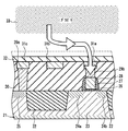
以下、本発明の実施の形態1にかかる半導体装置及び半導体装置の製造方法について、図1及び図2を参照しながら説明する。最初に、図1を用いて本実施の形態1にかかる半導体装置の構成について説明する。図1は、本発明の実施の形態1にかかる半導体装置の構成を部分的に示す断面図であり、図1(a)は半導体装置を構成する半導体基板の法線方向に沿って切断した断面図、図1(b)は図1(a)に示す切断線A−A´に沿って切断した断面図である。
【0036】
図1(a)に示すように、本実施の形態1にかかる半導体装置は、従来技術において図6に示した半導体装置と同様に、n型シリコン基板1を備えており、シリコン基板1には複数の素子分離2が、所定の間隔をおいて、シリコン基板1上に露出するように形成されている。
【0037】
また、シリコン基板1上の素子分離2間には、従来技術において図6に示した半導体装置と同様に、シリコン基板1の内部に形成されたpウェル(p well)3と、ゲート絶縁膜6と、n+ポリシリコンで形成されたゲート電極7と、シリコン基板1の表層部分に設けられたソース(n+)領域4a及びドレイン(n+)領域4bとによって、nチャンネルMOSトランジスタが形成されている。
【0038】
ゲート絶縁膜6及びゲート電極7は、従来技術において図6に示した半導体装置と同様に、互いに整合されるように形成されており、これらの両側面には、両側面を覆うようにサイドウォール8が形成されている。5は、n+領域であって、他のトランジスタのソース領域又はドレイン領域として機能する活性領域である。
【0039】
また、シリコン基板1の上には、従来技術において図6に示した半導体装置と同様に、多層配線を実現するための下地層間絶縁膜10と層間絶縁膜12とが順に積層されている。更に、下地層間絶縁膜10には、配線11a〜11cが形成されている。なお、下地層間絶縁膜10及び層間絶縁膜12は、シリコン酸化膜又はシリコン窒化膜である。
【0040】
配線11a〜11cは、ダマシン法によって同時に形成された銅配線(厚み500nm)であり、下地層間絶縁膜10に埋め込まれている。配線11aは、Wプラグ9cを介してゲート電極7に接続されるゲート電極接続用配線である。配線11cは、Wプラグ9aを介してn+領域5に接続されるソース・ドレイン接続用配線である。また、本実施の形態1においても、図1(b)に示すように、配線11a及び11cは短冊状に形成されている。
【0041】
配線11bは、ダマシン法で実施されるCMP工程における平坦性の確保のためのダミー配線であり、半導体装置の機能に貢献しない配線である。また、配線11bは、図1(b)に示すように、複数個で構成されており、正方形状に形成されている。
【0042】
このように、本実施の形態1にかかる半導体装置は、従来技術において図6に示した半導体装置と同様の構成を有しているが、以下に説明するように、この従来の半導体装置と異なる点を有している。
【0043】
本実施の形態1においては、従来技術において図6に示した半導体装置と異なり、ソース領域及びドレイン領域のいずれとしても機能しない活性領域(n+領域)13が、ゲート絶縁膜6が設けられたシリコン基板1の領域に隣接した位置に、素子分離2を隔てて設けられている。また、ダミー配線である配線11bは、電気的に浮遊した状態にはなく、Wプラグ9bを介して、この活性領域13に接続されている。
【0044】
なお、本明細書でいう「ソース領域及びドレイン領域のいずれとしても機能しない活性領域」とは、ソース領域及びドレイン領域と同様に形成されているが、これと隣接するゲート電極が存在しないためにソース領域及びドレイン領域のいずれとしても機能しない領域をいう。
【0045】
また、本実施の形態1においても、Wプラグ9a〜9cは、従来技術において図6に示したWプラグ29a及び29bと同様に、下地層間絶縁膜10に形成されたコンタクトホールに、タングステンを充填して形成されている。更に、本実施の形態1において、層間絶縁膜12には、多層配線のための配線及びプラグ(共に図示せず)が形成されており、層間絶縁膜12の上には別の複数の層間絶縁膜を形成することもできる。
【0046】
次に、図2に用いて、本実施の形態1にかかる半導体装置の製造方法及びダミー配線による作用について説明する。図2は、本発明の実施の形態1にかかる半導体装置の製造方法を示す断面図である。なお、図2は、図1に示す半導体装置を構成する層間絶縁膜の形成工程を示している。図2には、本実施の形態1によってプラズマチャージングダメージの発生が抑制される様子が概念的に示されている。
【0047】
最初に、素子分離2とpウェル3とが設けられたシリコン基板1上に、ゲート絶縁膜6を形成する。次に、ゲート絶縁膜6の上にゲート電極7を形成し、ゲート絶縁膜6及びゲート電極7の両側面にサイドウォール8を形成する。
【0048】
次いで、例えばAs、Pをイオン注入して、n+領域5、ソース(n+)領域4a及びドレイン(n+)領域4b、更に、活性領域13を形成する。その後、プラズマCVD装置(図示せず)によってプラズマを発生させて、下地層間絶縁膜10を成膜する。なお、このとき、ゲート電極7に接続される配線11aは未だ形成されていないため、プラズマによるチャージ電流は発生しない。
【0049】
次に、下地層間絶縁膜10において、底面にn+領域5が露出したコンタクトホール、底面に活性領域13が露出したコンタクトホール、底面にゲート電極7が露出したコンタクトホールを形成し、これらコンタクトホールの内部にタングステンを充填してWプラグ9a〜9cを形成する。
【0050】
その後、ダマシン法を用いて配線11a〜11cを同時に形成する。具体的には、下地層間絶縁膜10に、Wプラグ9a〜9cがそれぞれ底面に露出した溝を形成し、この溝が埋まるように銅の層を形成した後、CMP法による研磨によって余分な厚みを除去する。
【0051】
次に、図2に示すように、プラズマCVD装置(図示せず)によってプラズマ14を発生させて、層間絶縁膜12を成膜する。このとき、本実施の形態1においては、従来技術において示した図7の場合と異なり、ダミー配線となる配線11bはシリコン基板1に形成された活性領域13にWプラグ9bを介して電気的に接続されている。このため、プラズマ14による成膜時のチャージング電流は、ゲート電極7に接続された配線11aではなく、配線11bへと流れる。
【0052】
また、本実施の形態1においては、ダミー配線(配線11b)は、従来技術における特許文献1に開示された保護ダイオードではなく、活性領域13に電気的接続されている。更に、ダミー配線(配線11b)は、ゲート電極接続用配線(配線11a)に対して絶縁されている。このため、ゲート絶縁膜の薄膜化が更に進んだとしても、チャージング電流はダミー配線である配線11bへと流れることになる。
【0053】
このように、本実施の形態1によれば、薄膜化によってゲート絶縁膜の絶縁耐圧が低下した場合であっても、ゲート絶縁膜6の破壊によるデバイス特性の劣化を抑制できる。
【0054】
なお、本実施の形態1において、形成された全てのダミー配線が活性領域13に接続されていなくても良く、一部のダミー配線のみが活性領域13に接続された態様であっても良い。本実施の形態1において、形成されたダミー配線の活性領域13への接続割合は、ゲート絶縁膜6の厚み等といったプロセス条件に応じて適宜設定することができる。
【0055】
(実施の形態2)
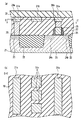
次に本発明の実施の形態2にかかる半導体装置及び半導体装置の製造方法について、図3及び図4を参照しながら説明する。最初に、図3を用いて本実施の形態2にかかる半導体装置の構成について説明する。図3は、本発明の実施の形態2にかかる半導体装置の構成を部分的に示す断面図であり、図3(a)は半導体装置を構成する半導体基板の法線方向に沿って切断した断面図、図3(b)は図1(a)に示す切断線B−B´に沿って切断した断面図である。なお、図3及び図4において、図1に示した符号と同様の符号が付された部分は、図1に示したものと同様のものである。
【0056】
図3に示すように、本実施の形態2においては、実施の形態1と異なり、第2のダミー配線となる配線11dが設けられている。配線11dも、ダマシン法によって、配線11a及び配線11bと同時に形成されているが、配線11dの全周囲は下地層間絶縁膜10と層間絶縁膜12とによって絶縁されており、配線11dは電気的に浮遊した状態にある。
【0057】
次に、図4に用いて、本実施の形態2にかかる半導体装置の製造方法及びダミー配線による作用について説明する。図4は、本発明の実施の形態2にかかる半導体装置の製造方法を示す断面図である。なお、図4は、図2に示す半導体装置を構成する層間絶縁膜の形成工程を示している。図4には、本実施の形態2によってプラズマチャージングダメージの発生が抑制される様子が概念的に示されている。
【0058】
最初に、実施の形態1と同様に、素子分離2とpウェル3とが設けられたシリコン基板1上にゲート絶縁膜6を形成し、更に、ゲート電極7及びサイドウォール8を形成する。
【0059】
次に、実施の形態1と同様に、イオン注入によって、ソース(n+)領域4a及びドレイン(n+)領域4bを形成し、更に、活性領域13を形成する。その後、プラズマCVD装置(図示せず)によってプラズマを発生させて、下地層間絶縁膜10を成膜する。その後、実施の形態1と同様に、下地層間絶縁膜10に、Wプラグ9b及び9cを形成した後、ダマシン法を用いて配線11a、11b及び11dを同時に形成する。
【0060】
次に、図4に示すように、プラズマCVD装置(図示せず)によってプラズマ14を発生させて、層間絶縁膜12を成膜する。このとき、本実施の形態2においても、実施の形態1において示した図2の場合と同様に、プラズマ14による成膜時のチャージング電流は、ゲート電極7に接続された配線11aではなく、配線11bへと流れる。
【0061】
但し、本実施の形態2においては、実施の形態1と異なり、活性領域13に接続された配線に隣接して配線11dが設けられている。このため、配線11bは、実施の形態1において示した場合よりも電荷を集め易い特性を備えることになる。
【0062】
即ち、本実施の形態2によれば、電気的に浮遊状態にある配線11dを、配線11bに隣接して配置することで、プラズマ14からのチャージング電流を選択的に配線11bに流すことができ、この結果、配線11bには実施の形態1で示した場合よりも多くのチャージング電流が流れることになる。このため、本実施の形態2によれば、実施の形態1よりも、デバイス特性劣化の抑制効果を更に高めることができる。
【0063】
また、本実施の形態2においては、図3(b)に示すように、第2のダミー配線となる配線11dは、複数の配線で構成されている。更に、複数の配線11dは、活性領域13に接続された配線(ダミー配線)11bに隣接するように形成されており、配線11bにおける配線11a(ゲート電極用配線)に隣接していない側において、配線11bを囲むように配置されている。このため、配線11bへのチャージング電流の集中を効率的に行うことができる。
【0064】
本実施の形態2において、第2のダミー配線である配線11dのレイアウトは、図3(b)に示すレイアウトに限定されるものではない。配線11dのレイアウトは、CMP工程でのプロセス特性やダミー配線ルール等に応じて適宜設定すれば良い。
【0065】
ここで、上述した実施の形態1及び実施の形態2にかかる半導体装置及び半導体装置の製造方法の効果について、図5を用いて説明する。図5は、実施の形態1及び実施の形態2にかかる半導体装置の寿命を示すグラフである。
【0066】
図5において、横軸は、信頼性寿命の指標となる定電圧TDDB(Time Dependent Dielectric Breakdown)試験時の半導体装置の寿命を示しており、縦軸は、ワイブル分布を仮定した累積不良率を示している。また、図5中の「従来の半導体装置」は、図6に示す半導体装置を示している。従来の半導体装置、実施の形態1及び2の半導体装置のいずれにおいても、ゲート絶縁膜の厚みは2.2nmである。
【0067】
図5から分かるように、累積不良率が同一の場合、従来の半導体装置(図中「○」)の破壊までの時間は、本発明の実施の形態1にかかる半導体装置(図中「□」)及び実施の形態2にかかる半導体装置(図中「●」)の破壊までの時間に比べて、常に短くなっている。このことは、本発明の実施の形態1にかかる半導体装置(図中「□」)及び実施の形態2にかかる半導体装置(図中「●」)は、従来の半導体装置(図中「○」)に比べて、寿命が長いことを示している。つまり、本発明の半導体装置及び半導体装置の製造方法によれば、デバイス特性の劣化を抑制できる。
【0068】
なお、本発明の半導体装置及び半導体装置の製造方法は、上記した実施の形態1及び2に限定されるものではない。例えば、実施の形態1及び2においては、CMP工程における効果を高めるため、又ルール化し易いようにするため、ダミー配線の形状は矩形としているが、本発明においてはダミー配線の形状は特に限定されるものではない。
【0069】
本発明においては、ダミー配線は、ソース領域及びドレイン領域のいずれとしても機能しない活性領域に電気的に接続されたものであれば良い。また、ダミー配線が接続される活性領域のタイプはn型に限定されず、p型であっても良い。更に、本発明においては、半導体基板は、p型シリコン基板であっても良いし、シリコン基板以外の基板であっても良い。
【0070】
また、実施の形態1及び2においては、ダミー配線と活性領域との接続や、ゲート電極接続用配線とゲート電極との接続等においては、Wプラグが用いられているが、Cuプラグを用いることもできる。更に、このようなプラグを設ける代わりに、デュアルダマシン構造とすることもできる。
【0071】
また、実施の形態1及び2においては、配線はCu配線であるが、本発明はこれにも限定されず、配線は金属材料で形成されたものであれば良く、Al配線であっても良い。Al配線の場合は、配線はエッチングにより形成すれば良い。また、この場合は、ダミー配線は、エッチングを実施する前に行うリソグラフィー法におけるアライメント確認のためのアライメント用配線であっても良い。
【0072】
【発明の効果】
以上のように、本発明にかかる半導体装置及び半導体装置の製造方法によれば、配線の周りに配置するダミー配線の構造を最適化することにより、層間絶縁膜をプラズマプロセスで作成する際のチャージングダメージの抑制を図ることができる。その結果、信頼性の高い半導体装置及びその製造方法を提供することができる。
【図面の簡単な説明】
【図1】本発明の実施の形態1にかかる半導体装置の構成を部分的に示す断面図であり、図1(a)は半導体装置を構成する半導体基板の法線方向に沿って切断した断面図、図1(b)は図1(a)に示す切断線A−A´に沿って切断した断面図である。
【図2】本発明の実施の形態1にかかる半導体装置の製造方法を示す断面図である。
【図3】本発明の実施の形態2にかかる半導体装置の構成を部分的に示す断面図であり、図3(a)は半導体装置を構成する半導体基板の法線方向に沿って切断した断面図、図3(b)は図1(a)に示す切断線B−B´に沿って切断した断面図である。
【図4】本発明の実施の形態2にかかる半導体装置の製造方法を示す断面図である。
【図5】実施の形態1及び実施の形態2にかかる半導体装置の寿命を示すグラフである。
【図6】従来の半導体装置の構成を部分的に示す断面図であり、図6(a)は半導体装置を構成する半導体基板の法線方向に沿って切断した断面図、図6(b)は図6(a)に示す切断線C−C´に沿って切断した断面図である。
【図7】図6に示す従来の半導体装置における層間絶縁膜の形成工程を示す断面図であり、プラズマチャージングダメージの発生を概念的に示している。
【符号の説明】
1 n型シリコン基板
2 素子分離
3 pウェル
4a ソース(n+)領域
4b ドレイン(n+)領域
5 n+領域
6 ゲート絶縁膜
7 ゲート電極
8 サイドウォール
9a〜9c Wプラグ
10 下地層間絶縁膜
11a 配線(ゲート電極接続用配線)
11b 配線(ダミー配線)
11c 配線(ソース・ドレイン接続用配線)
11d 配線(第2のダミー配線)
12 層間絶縁膜
13 活性領域(n+領域)[0001]
TECHNICAL FIELD OF THE INVENTION
The present invention relates to a semiconductor device and a method for manufacturing the same.
[0002]
[Prior art]
2. Description of the Related Art In recent years, high integration of a semiconductor device including a semiconductor integrated circuit has been greatly advanced. In particular, in a MIS (Metal Insulated Semiconductor) type semiconductor device, elements such as transistors have been miniaturized and improved in performance in order to cope with higher integration, and further miniaturization and higher performance have been demanded. Have been.
[0003]
In the process of forming wiring of such a semiconductor device, use of a plasma process represented by plasma CVD or plasma etching is increasing. This is because the amount of heat treatment is limited in the step of forming wiring of a semiconductor device in terms of diffusion of impurities and heat resistance of metal wiring materials, and the amount of heat treatment can be reduced by the plasma process.
[0004]
Furthermore, in recent years, copper (Cu) wiring may be introduced in order to improve the performance. However, since a damascene method is used for forming the copper (Cu) wiring, in this case, plasma is increasingly used. Increased use of the process.
[0005]
As described above, the plasma process is frequently used not only at the time of etching but also at the time of film formation, and the use of the plasma process is increasing every year. However, as the use of the plasma process increases, device damage due to the plasma process has become apparent. This is mainly referred to as "plasma charging damage" and has been greatly increased in recent years.
[0006]
A semiconductor device that has suffered such plasma charging damage has poor device characteristics and is therefore defective. In the problem of plasma charging damage, deterioration of reliability of the gate insulating film has become a serious problem.
[0007]
Here, the plasma charging damage will be described with reference to FIGS. FIG. 6 is a cross-sectional view partially showing the structure of a conventional semiconductor device, and FIG. 6A is a cross-sectional view taken along a normal direction of a semiconductor substrate forming the semiconductor device, and FIG. FIG. 7 is a cross-sectional view taken along a cutting line CC ′ shown in FIG.
[0008]
As shown in FIG. 6A, the conventional semiconductor device includes an n-
[0009]
A p-well (p-well) 23 formed inside the
[0010]
The
[0011]
On the
[0012]
The
[0013]
The
[0014]
The
[0015]
FIG. 7 is a cross-sectional view showing a step of forming an interlayer insulating film in the conventional semiconductor device shown in FIG. 6, and conceptually shows occurrence of plasma charging damage.
[0016]
First, a
[0017]
Next, after forming the
[0018]
Next, as shown in FIG. 7, a
[0019]
In order to solve such a problem,
[0020]
[Patent Document 1]
JP-A-10-173157 (Paragraph 20, FIG. 2 to FIG. 9)
[0021]
[Problems to be solved by the invention]
However, with the increase in the degree of integration of semiconductor devices, gate insulating films are becoming thinner year by year. As a result, the withstand voltage of the gate insulating film is becoming smaller than the junction withstand voltage of the protection diode. Therefore, as the thickness of the gate insulating film is reduced, a charging current leaking to the gate electrode without flowing through the protection diode is increasing.
[0022]
From this, the effect of suppressing the plasma charging damage by the protection diode becomes smaller as the gate insulating film becomes thinner, and despite the provision of the protection diode, the device characteristics due to the plasma charging damage are reduced. Has deteriorated.
[0023]
SUMMARY OF THE INVENTION An object of the present invention is to provide a semiconductor device which can solve the above problem and can suppress plasma charging damage in a plasma process, and a method of manufacturing the same.
[0024]
[Means for Solving the Problems]
In order to achieve the above object, a semiconductor device according to the present invention includes a semiconductor substrate, a gate insulating film provided on the semiconductor substrate, a gate electrode provided on the gate insulating film, and a gate insulating film. A semiconductor device having an insulating layer covering the gate electrode, and a wiring provided on the insulating layer, wherein the wiring is a gate electrode wiring electrically connected to the gate electrode, and a dummy wiring Wherein the dummy wiring is electrically connected to an active region formed in the semiconductor substrate.
[0025]
According to the semiconductor device of the present invention, the dummy wiring is electrically connected to the active region formed on the silicon substrate. Therefore, the charging current due to the plasma flows not to the gate electrode wiring but to the dummy wiring. Further, the dummy wiring is electrically connected to the active region instead of the protection diode disclosed in
[0026]
In the semiconductor device according to the present invention, it is preferable that the active region to which the dummy wiring is connected is an active region that does not function as any of a source region and a drain region. In this case, an active region functioning as a source region or a drain region is formed in the semiconductor substrate, and the wiring further includes a wiring electrically connected to the active region functioning as the source or drain region. Preferably.
[0027]
Further, in the semiconductor device according to the present invention, the wiring further has a second dummy wiring, and the second dummy wiring is formed at a position adjacent to the dummy wiring. It is preferable that the entire periphery of the dummy wiring is insulated by the insulating layer. In this case, the dummy wiring is arranged at a position adjacent to the gate electrode wiring, the second dummy wiring is composed of a plurality of wirings, and the plurality of wirings constituting the second dummy wiring are: It is preferable that the dummy wiring is arranged so as to surround the dummy wiring on a side not adjacent to the gate electrode wiring.
[0028]
Further, in the semiconductor device according to the present invention, the wiring is formed by a damascene method, and is embedded in the insulating layer, and the active region to which the dummy wiring is connected has a gate insulating property. It is preferable that the semiconductor device is provided at a position adjacent to a region of the semiconductor substrate on which a film is provided, with an element isolation therebetween.
[0029]
Further, it is preferable that the gate electrode wiring, the dummy wiring, and the second dummy wiring are formed of the same metal material, and examples of the metal material include a metal material containing copper.
[0030]
Next, in order to achieve the above object, a method for manufacturing a semiconductor device according to the present invention includes: (a) forming at least a stacked body of a gate insulating film and a gate electrode and an active region on a semiconductor substrate; (B) forming a first insulating layer covering the stacked body and the active region on the semiconductor substrate; and (c) electrically connecting the first insulating layer to the gate electrode. Simultaneously providing a gate electrode wiring and a dummy wiring electrically connected to the active region; and (d) forming a second insulating layer on the first insulating layer by a plasma process. And a step of performing
[0031]
According to the method for manufacturing a semiconductor device according to the present invention, the second insulating layer is formed while the dummy wiring is electrically connected to the active region formed on the silicon substrate. For this reason, the charging current generated when the second insulating layer is formed by the plasma flows to the dummy wiring instead of the gate electrode wiring. Further, the dummy wiring is electrically connected to the active region instead of the protection diode disclosed in
[0032]
In the method of manufacturing a semiconductor device according to the present invention, in the step (d), while discharging the charging current from the plasma generated by the plasma process through the dummy wiring, the second insulating layer is removed. Preferably, it is formed. In the step (c), it is preferable that the gate electrode wiring and the dummy wiring are formed by a damascene method.
[0033]
In the method of manufacturing a semiconductor device according to the present invention, in the step (a), the active region functioning as a source region or a drain region and the active region functioning as neither the source region nor the drain region may be formed. It is preferable that, in the step (c), the dummy wiring is connected to an active region that does not function as any of the source region and the drain region. Further, it is preferable that the first insulating layer is a base interlayer insulating film for forming a multilayer wiring, and the second insulating layer is an interlayer insulating film for forming a multilayer wiring.
[0034]
Further, in the method of manufacturing a semiconductor device according to the present invention, in the step (c), the first insulating layer may insulate the gate electrode and the active region at a position adjacent to the dummy wiring. Preferably, the formed second dummy wiring is formed simultaneously with the gate electrode wiring. Further, it is preferable that the first insulating layer and the second insulating layer are a silicon oxide film or a silicon nitride film.
[0035]
BEST MODE FOR CARRYING OUT THE INVENTION
(Embodiment 1)
Hereinafter, a semiconductor device and a method of manufacturing the semiconductor device according to the first embodiment of the present invention will be described with reference to FIGS. First, the configuration of the semiconductor device according to the first embodiment will be described with reference to FIG. FIG. 1 is a cross-sectional view partially showing a configuration of a semiconductor device according to a first embodiment of the present invention. FIG. 1A is a cross-sectional view taken along a normal direction of a semiconductor substrate forming the semiconductor device. FIG. 1B is a cross-sectional view taken along a cutting line AA ′ shown in FIG.
[0036]
As shown in FIG. 1A, the semiconductor device according to the first embodiment includes an n-
[0037]
In addition, between the
[0038]
The
[0039]
Further, on the
[0040]
The
[0041]
The
[0042]
As described above, the semiconductor device according to the first embodiment has the same configuration as the semiconductor device shown in FIG. 6 in the related art, but differs from the conventional semiconductor device as described below. Have a point.
[0043]
In the first embodiment, unlike the semiconductor device shown in FIG. 6 in the related art, an active region (n + region) 13 that does not function as any of a source region and a drain region is formed of silicon provided with a
[0044]
Note that the “active region that does not function as any of the source region and the drain region” in this specification is formed in the same manner as the source region and the drain region, but has no gate electrode adjacent thereto. A region that does not function as either a source region or a drain region.
[0045]
Also, in the first embodiment, W plugs 9a to 9c are filled with tungsten in contact holes formed in base
[0046]
Next, a method of manufacturing the semiconductor device according to the first embodiment and the operation of the dummy wiring will be described with reference to FIG. FIG. 2 is a sectional view illustrating the method for manufacturing the semiconductor device according to the first embodiment of the present invention. FIG. 2 shows a step of forming an interlayer insulating film constituting the semiconductor device shown in FIG. FIG. 2 conceptually shows a state in which occurrence of plasma charging damage is suppressed by the first embodiment.
[0047]
First, a
[0048]
Next, for example, As and P are ion-implanted to form an n + region 5, a source (n +)
[0049]
Next, in the underlying
[0050]
After that, the
[0051]
Next, as shown in FIG. 2, a
[0052]
In the first embodiment, the dummy wiring (
[0053]
As described above, according to the first embodiment, even when the withstand voltage of the gate insulating film is reduced due to the thinning, deterioration of the device characteristics due to the destruction of the
[0054]
In the first embodiment, not all of the formed dummy wires may be connected to the
[0055]
(Embodiment 2)
Next, a semiconductor device and a method of manufacturing the semiconductor device according to a second embodiment of the present invention will be described with reference to FIGS. First, the configuration of the semiconductor device according to the second embodiment will be described with reference to FIG. FIG. 3 is a cross-sectional view partially showing a configuration of a semiconductor device according to a second embodiment of the present invention. FIG. 3A is a cross-sectional view taken along a normal direction of a semiconductor substrate forming the semiconductor device. FIG. 3B is a cross-sectional view taken along a cutting line BB ′ shown in FIG. In FIGS. 3 and 4, portions denoted by the same reference numerals as those shown in FIG. 1 are the same as those shown in FIG.
[0056]
As shown in FIG. 3, the second embodiment differs from the first embodiment in that a
[0057]
Next, a method of manufacturing the semiconductor device according to the second embodiment and the operation of the dummy wiring will be described with reference to FIG. FIG. 4 is a sectional view illustrating the method for manufacturing the semiconductor device according to the second embodiment of the present invention. FIG. 4 shows a step of forming an interlayer insulating film constituting the semiconductor device shown in FIG. FIG. 4 conceptually shows how plasma charging damage is suppressed from occurring according to the second embodiment.
[0058]
First, as in the first embodiment, a
[0059]
Next, as in the first embodiment, a source (n +)
[0060]
Next, as shown in FIG. 4, a
[0061]
However, in the second embodiment, unlike the first embodiment, the
[0062]
That is, according to the second embodiment, the charging current from the
[0063]
In the second embodiment, as shown in FIG. 3B, the
[0064]
In the second embodiment, the layout of the
[0065]
Here, the effects of the semiconductor device and the method of manufacturing the semiconductor device according to the first and second embodiments will be described with reference to FIG. FIG. 5 is a graph illustrating the life of the semiconductor device according to the first and second embodiments.
[0066]
In FIG. 5, the horizontal axis represents the life of the semiconductor device at the time of a constant voltage TDDB (Time Dependent Breakdown) test, which is an index of the reliability life, and the vertical axis represents the cumulative failure rate assuming a Weibull distribution. ing. "Conventional semiconductor device" in FIG. 5 indicates the semiconductor device shown in FIG. In each of the conventional semiconductor device and the semiconductor devices of
[0067]
As can be seen from FIG. 5, when the cumulative failure rate is the same, the time until destruction of the conventional semiconductor device (“O” in the figure) is equal to the time required for the semiconductor device according to the first embodiment of the present invention (“□” in the figure). ) And the time until destruction of the semiconductor device according to the second embodiment (“●” in the figure) is always shorter. This means that the semiconductor device according to the first embodiment of the present invention (“□” in the drawing) and the semiconductor device according to the second embodiment (“●” in the drawing) are different from the conventional semiconductor device (“○” in the drawing). ) Indicates that the life is longer. That is, according to the semiconductor device and the method for manufacturing the semiconductor device of the present invention, it is possible to suppress the deterioration of the device characteristics.
[0068]
Note that the semiconductor device and the method of manufacturing the semiconductor device of the present invention are not limited to the first and second embodiments. For example, in the first and second embodiments, the shape of the dummy wiring is rectangular in order to enhance the effect in the CMP process and to facilitate the rule, but in the present invention, the shape of the dummy wiring is not particularly limited. Not something.
[0069]
In the present invention, it is sufficient that the dummy wiring is electrically connected to an active region that does not function as any of the source region and the drain region. The type of the active region to which the dummy wiring is connected is not limited to n-type, but may be p-type. Further, in the present invention, the semiconductor substrate may be a p-type silicon substrate or a substrate other than a silicon substrate.
[0070]
In the first and second embodiments, the W plug is used for the connection between the dummy wiring and the active region and the connection between the gate electrode connection wiring and the gate electrode, but the Cu plug is used. You can also. Further, instead of providing such a plug, a dual damascene structure may be employed.
[0071]
Further, in the first and second embodiments, the wiring is a Cu wiring, but the present invention is not limited to this. The wiring may be any one formed of a metal material, and may be an Al wiring. . In the case of an Al wiring, the wiring may be formed by etching. In this case, the dummy wiring may be an alignment wiring for confirming alignment in a lithography method performed before performing etching.
[0072]
【The invention's effect】
As described above, according to the semiconductor device and the method of manufacturing the semiconductor device according to the present invention, by optimizing the structure of the dummy wiring disposed around the wiring, the charge in forming the interlayer insulating film by the plasma process can be improved. Wing damage can be suppressed. As a result, a highly reliable semiconductor device and a method for manufacturing the same can be provided.
[Brief description of the drawings]
FIG. 1 is a cross-sectional view partially showing a configuration of a semiconductor device according to a first embodiment of the present invention, and FIG. 1A is a cross-section taken along a normal direction of a semiconductor substrate forming the semiconductor device; FIG. 1B is a cross-sectional view taken along a cutting line AA ′ shown in FIG.
FIG. 2 is a sectional view illustrating the method for manufacturing the semiconductor device according to the first embodiment of the present invention;
FIG. 3 is a cross-sectional view partially showing a configuration of a semiconductor device according to a second embodiment of the present invention; FIG. 3A is a cross-sectional view taken along a normal direction of a semiconductor substrate forming the semiconductor device; FIG. 3B is a cross-sectional view taken along a cutting line BB ′ shown in FIG.
FIG. 4 is a sectional view illustrating the method for manufacturing the semiconductor device according to the second embodiment of the present invention;
FIG. 5 is a graph showing the life of the semiconductor device according to the first and second embodiments.
6A and 6B are cross-sectional views partially showing a configuration of a conventional semiconductor device. FIG. 6A is a cross-sectional view taken along a normal direction of a semiconductor substrate forming the semiconductor device, and FIG. FIG. 7 is a cross-sectional view taken along a cutting line CC ′ shown in FIG.
7 is a cross-sectional view showing a step of forming an interlayer insulating film in the conventional semiconductor device shown in FIG. 6, conceptually showing the occurrence of plasma charging damage.
[Explanation of symbols]
1 n-type silicon substrate
2 Element separation
3 p-well
4a Source (n +) area
4b Drain (n +) region
5 n + area
6 Gate insulating film
7 Gate electrode
8 Side wall
9a-9c W plug
10 Underlayer insulating film
11a Wiring (Gate electrode connection wiring)
11b Wiring (dummy wiring)
11c wiring (wiring for source / drain connection)
11d wiring (second dummy wiring)
12 interlayer insulating film
13 Active area (n + area)
Claims (15)
前記配線は、前記ゲート電極に電気的に接続されたゲート電極用配線と、ダミー配線とを有し、
前記ダミー配線は、前記半導体基板に形成された活性領域に電気的に接続されていることを特徴とする半導体装置。A semiconductor substrate, a gate insulating film provided on the semiconductor substrate, a gate electrode provided on the gate insulating film, an insulating layer covering the gate insulating film and the gate electrode, and A semiconductor device having provided wiring,
The wiring has a wiring for a gate electrode electrically connected to the gate electrode, and a dummy wiring,
The semiconductor device according to claim 1, wherein the dummy wiring is electrically connected to an active region formed on the semiconductor substrate.
前記第2のダミー配線は、前記ダミー配線と隣接する位置に形成されており、前記第2のダミー配線の全周囲は前記絶縁層によって絶縁されている請求項1記載の半導体装置。The wiring further includes a second dummy wiring;
2. The semiconductor device according to claim 1, wherein the second dummy wiring is formed at a position adjacent to the dummy wiring, and the entire periphery of the second dummy wiring is insulated by the insulating layer. 3.
前記第2のダミー配線が複数の配線で構成され、前記第2のダミー配線を構成する複数の配線が、前記ダミー配線の前記ゲート電極用配線に隣接していない側において、前記ダミー配線を囲むように配置されている請求項3記載の半導体装置。The dummy wiring is arranged at a position adjacent to the gate electrode wiring,
The second dummy wiring includes a plurality of wirings, and the plurality of wirings forming the second dummy wiring surround the dummy wiring on a side of the dummy wiring not adjacent to the gate electrode wiring. 4. The semiconductor device according to claim 3, wherein the semiconductor device is arranged as follows.
前記ダミー配線が接続された活性領域が、前記ゲート絶縁膜が設けられた前記半導体基板の領域に隣接した位置に、素子分離を隔てて設けられている請求項1〜4のいずれかに記載の半導体装置。The wiring is formed by a damascene method, and is embedded in the insulating layer;
The device according to claim 1, wherein the active region to which the dummy wiring is connected is provided at a position adjacent to a region of the semiconductor substrate on which the gate insulating film is provided, with an element isolation therebetween. Semiconductor device.
前記配線が、前記ソース領域又はドレイン領域として機能する活性領域に電気的に接続された配線を更に有している請求項2記載の半導体装置。An active region functioning as a source region or a drain region is formed in the semiconductor substrate,
The semiconductor device according to claim 2, wherein the wiring further includes a wiring electrically connected to an active region functioning as the source region or the drain region.
(b)前記半導体基板上に、前記積層体及び前記活性領域を被覆する第1の絶縁層を形成する工程と、
(c)前記第1の絶縁層に、前記ゲート電極に電気的に接続されるゲート電極用配線と、前記活性領域に電気的に接続されるダミー配線とを同時に設ける工程と、
(d)前記第1の絶縁層の上に、プラズマプロセスによって、第2の絶縁層を形成する工程とを有する半導体装置の製造方法。(A) forming at least a stacked body of a gate insulating film and a gate electrode and an active region on a semiconductor substrate;
(B) forming a first insulating layer covering the stacked body and the active region on the semiconductor substrate;
(C) simultaneously providing, on the first insulating layer, a gate electrode wiring electrically connected to the gate electrode and a dummy wiring electrically connected to the active region;
(D) forming a second insulating layer on the first insulating layer by a plasma process.
前記(c)の工程において、前記ソース領域及びドレイン領域のいずれとしても機能しない活性領域に前記ダミー配線を接続する請求項9記載の半導体装置の製造方法。In the step (a), an active region functioning as a source region or a drain region and an active region not functioning as any of the source region and the drain region are formed;
10. The method of manufacturing a semiconductor device according to claim 9, wherein in the step (c), the dummy wiring is connected to an active region that does not function as any of the source region and the drain region.
Priority Applications (6)
| Application Number | Priority Date | Filing Date | Title |
|---|---|---|---|
| JP2003158478A JP2004363254A (en) | 2003-06-03 | 2003-06-03 | Semiconductor device and its fabricating process |
| US10/859,921 US20050006707A1 (en) | 2003-06-03 | 2004-06-02 | Semiconductor device and method for manufacturing the same |
| TW093115723A TWI241659B (en) | 2003-06-03 | 2004-06-02 | Semiconductor device and method for manufacturing the same |
| CNB2004100462933A CN100370623C (en) | 2003-06-03 | 2004-06-03 | Semiconductor device and method for manufacturing the same |
| US11/620,976 US7432556B2 (en) | 2003-06-03 | 2007-01-08 | Semiconductor device with dummy conductors |
| US12/201,991 US20090001473A1 (en) | 2003-06-03 | 2008-08-29 | Semiconductor device and method for manufacturing the same |
Applications Claiming Priority (1)
| Application Number | Priority Date | Filing Date | Title |
|---|---|---|---|
| JP2003158478A JP2004363254A (en) | 2003-06-03 | 2003-06-03 | Semiconductor device and its fabricating process |
Publications (1)
| Publication Number | Publication Date |
|---|---|
| JP2004363254A true JP2004363254A (en) | 2004-12-24 |
Family
ID=34051870
Family Applications (1)
| Application Number | Title | Priority Date | Filing Date |
|---|---|---|---|
| JP2003158478A Pending JP2004363254A (en) | 2003-06-03 | 2003-06-03 | Semiconductor device and its fabricating process |
Country Status (1)
| Country | Link |
|---|---|
| JP (1) | JP2004363254A (en) |
Cited By (1)
| Publication number | Priority date | Publication date | Assignee | Title |
|---|---|---|---|---|
| JP2016500481A (en) * | 2012-12-14 | 2016-01-12 | スパンション エルエルシー | Process charge protection for split gate charge trap flash |
Citations (6)
| Publication number | Priority date | Publication date | Assignee | Title |
|---|---|---|---|---|
| JPH03291934A (en) * | 1990-04-09 | 1991-12-24 | Toshiba Corp | Manufacture of semiconductor device |
| JPH05166946A (en) * | 1991-12-19 | 1993-07-02 | Toshiba Corp | Manufacture of semiconductor device |
| JPH0974200A (en) * | 1995-07-04 | 1997-03-18 | Matsushita Electric Ind Co Ltd | Mis semiconductor device and its manufacture |
| JPH1174523A (en) * | 1997-06-19 | 1999-03-16 | Toshiba Corp | Semiconductor device and its manufacture |
| JP2000223492A (en) * | 1999-01-29 | 2000-08-11 | Nec Corp | Manufacture of semiconductor device having multilayer wiring |
| JP2001110810A (en) * | 1999-10-06 | 2001-04-20 | Fujitsu Ltd | Semiconductor device and its manufacturing method |
-
2003
- 2003-06-03 JP JP2003158478A patent/JP2004363254A/en active Pending
Patent Citations (6)
| Publication number | Priority date | Publication date | Assignee | Title |
|---|---|---|---|---|
| JPH03291934A (en) * | 1990-04-09 | 1991-12-24 | Toshiba Corp | Manufacture of semiconductor device |
| JPH05166946A (en) * | 1991-12-19 | 1993-07-02 | Toshiba Corp | Manufacture of semiconductor device |
| JPH0974200A (en) * | 1995-07-04 | 1997-03-18 | Matsushita Electric Ind Co Ltd | Mis semiconductor device and its manufacture |
| JPH1174523A (en) * | 1997-06-19 | 1999-03-16 | Toshiba Corp | Semiconductor device and its manufacture |
| JP2000223492A (en) * | 1999-01-29 | 2000-08-11 | Nec Corp | Manufacture of semiconductor device having multilayer wiring |
| JP2001110810A (en) * | 1999-10-06 | 2001-04-20 | Fujitsu Ltd | Semiconductor device and its manufacturing method |
Cited By (1)
| Publication number | Priority date | Publication date | Assignee | Title |
|---|---|---|---|---|
| JP2016500481A (en) * | 2012-12-14 | 2016-01-12 | スパンション エルエルシー | Process charge protection for split gate charge trap flash |
Similar Documents
| Publication | Publication Date | Title |
|---|---|---|
| JP4875622B2 (en) | Manufacturing method of semiconductor device | |
| US7633126B2 (en) | Semiconductor device having a shared contact and method of fabricating the same | |
| US7432556B2 (en) | Semiconductor device with dummy conductors | |
| JP4996166B2 (en) | Semiconductor device and manufacturing method of semiconductor device | |
| US7411240B2 (en) | Integrated circuits including spacers that extend beneath a conductive line | |
| US8050066B2 (en) | MISFET with capacitors | |
| JP6700565B2 (en) | Semiconductor device | |
| JP2009117710A (en) | Semiconductor chip and semiconductor device | |
| US20030080429A1 (en) | Semiconductor device | |
| JP2004152929A (en) | Semiconductor device and its manufacturing device | |
| CN109786319B (en) | FDSOI semiconductor device with contact enhancement layer and method of manufacture | |
| US7719113B2 (en) | Semiconductor device including dummy patterns | |
| US8941182B2 (en) | Buried sublevel metallizations for improved transistor density | |
| US20220367452A1 (en) | Semiconductor structure and method of forming thereof | |
| JP2006344773A (en) | Semiconductor device and its manufacturing method | |
| JP2011044625A (en) | Semiconductor device, and method of manufacturing semiconductor device | |
| JP2004363254A (en) | Semiconductor device and its fabricating process | |
| JP4601919B2 (en) | Manufacturing method of semiconductor device | |
| JP2008078331A (en) | Semiconductor device | |
| JP2004134498A (en) | Semiconductor integrated circuit device and its manufacturing method | |
| JP2007214161A (en) | Semiconductor device and method of manufacturing same | |
| US9070564B2 (en) | Semiconductor device having mixedly mounted components with common film layers and method of manufacturing the same | |
| JP2000349259A (en) | Semiconductor device and manufacture thereof | |
| JP2014011165A (en) | Semiconductor device manufacturing method | |
| JP2005032863A (en) | Semiconductor device |
Legal Events
| Date | Code | Title | Description |
|---|---|---|---|
| A621 | Written request for application examination |
Free format text: JAPANESE INTERMEDIATE CODE: A621 Effective date: 20060412 |
|
| A977 | Report on retrieval |
Effective date: 20080331 Free format text: JAPANESE INTERMEDIATE CODE: A971007 |
|
| A131 | Notification of reasons for refusal |
Effective date: 20091105 Free format text: JAPANESE INTERMEDIATE CODE: A131 |
|
| A521 | Written amendment |
Free format text: JAPANESE INTERMEDIATE CODE: A523 Effective date: 20091224 |
|
| A02 | Decision of refusal |
Effective date: 20100216 Free format text: JAPANESE INTERMEDIATE CODE: A02 |
|
| A521 | Written amendment |
Free format text: JAPANESE INTERMEDIATE CODE: A523 Effective date: 20100514 |
|
| A911 | Transfer of reconsideration by examiner before appeal (zenchi) |
Effective date: 20100524 Free format text: JAPANESE INTERMEDIATE CODE: A911 |
|
| A912 | Removal of reconsideration by examiner before appeal (zenchi) |
Effective date: 20100709 Free format text: JAPANESE INTERMEDIATE CODE: A912 |