JP6697372B2 - Dry etching method and semiconductor device manufacturing method - Google Patents
Dry etching method and semiconductor device manufacturing method Download PDFInfo
- Publication number
- JP6697372B2 JP6697372B2 JP2016226298A JP2016226298A JP6697372B2 JP 6697372 B2 JP6697372 B2 JP 6697372B2 JP 2016226298 A JP2016226298 A JP 2016226298A JP 2016226298 A JP2016226298 A JP 2016226298A JP 6697372 B2 JP6697372 B2 JP 6697372B2
- Authority
- JP
- Japan
- Prior art keywords
- conductive member
- insulating film
- bias power
- power
- etching
- Prior art date
- Legal status (The legal status is an assumption and is not a legal conclusion. Google has not performed a legal analysis and makes no representation as to the accuracy of the status listed.)
- Active
Links
Images


Classifications
-
- H—ELECTRICITY
- H01—ELECTRIC ELEMENTS
- H01J—ELECTRIC DISCHARGE TUBES OR DISCHARGE LAMPS
- H01J37/00—Discharge tubes with provision for introducing objects or material to be exposed to the discharge, e.g. for the purpose of examination or processing thereof
- H01J37/32—Gas-filled discharge tubes
- H01J37/32431—Constructional details of the reactor
- H01J37/32697—Electrostatic control
- H01J37/32706—Polarising the substrate
-
- H—ELECTRICITY
- H01—ELECTRIC ELEMENTS
- H01L—SEMICONDUCTOR DEVICES NOT COVERED BY CLASS H10
- H01L21/00—Processes or apparatus adapted for the manufacture or treatment of semiconductor or solid state devices or of parts thereof
- H01L21/02—Manufacture or treatment of semiconductor devices or of parts thereof
- H01L21/04—Manufacture or treatment of semiconductor devices or of parts thereof the devices having at least one potential-jump barrier or surface barrier, e.g. PN junction, depletion layer or carrier concentration layer
- H01L21/18—Manufacture or treatment of semiconductor devices or of parts thereof the devices having at least one potential-jump barrier or surface barrier, e.g. PN junction, depletion layer or carrier concentration layer the devices having semiconductor bodies comprising elements of Group IV of the Periodic System or AIIIBV compounds with or without impurities, e.g. doping materials
- H01L21/30—Treatment of semiconductor bodies using processes or apparatus not provided for in groups H01L21/20 - H01L21/26
- H01L21/31—Treatment of semiconductor bodies using processes or apparatus not provided for in groups H01L21/20 - H01L21/26 to form insulating layers thereon, e.g. for masking or by using photolithographic techniques; After treatment of these layers; Selection of materials for these layers
- H01L21/3105—After-treatment
- H01L21/311—Etching the insulating layers by chemical or physical means
- H01L21/31105—Etching inorganic layers
- H01L21/31111—Etching inorganic layers by chemical means
- H01L21/31116—Etching inorganic layers by chemical means by dry-etching
-
- H—ELECTRICITY
- H01—ELECTRIC ELEMENTS
- H01L—SEMICONDUCTOR DEVICES NOT COVERED BY CLASS H10
- H01L21/00—Processes or apparatus adapted for the manufacture or treatment of semiconductor or solid state devices or of parts thereof
- H01L21/02—Manufacture or treatment of semiconductor devices or of parts thereof
- H01L21/04—Manufacture or treatment of semiconductor devices or of parts thereof the devices having at least one potential-jump barrier or surface barrier, e.g. PN junction, depletion layer or carrier concentration layer
- H01L21/18—Manufacture or treatment of semiconductor devices or of parts thereof the devices having at least one potential-jump barrier or surface barrier, e.g. PN junction, depletion layer or carrier concentration layer the devices having semiconductor bodies comprising elements of Group IV of the Periodic System or AIIIBV compounds with or without impurities, e.g. doping materials
- H01L21/30—Treatment of semiconductor bodies using processes or apparatus not provided for in groups H01L21/20 - H01L21/26
- H01L21/31—Treatment of semiconductor bodies using processes or apparatus not provided for in groups H01L21/20 - H01L21/26 to form insulating layers thereon, e.g. for masking or by using photolithographic techniques; After treatment of these layers; Selection of materials for these layers
- H01L21/3205—Deposition of non-insulating-, e.g. conductive- or resistive-, layers on insulating layers; After-treatment of these layers
- H01L21/321—After treatment
- H01L21/3213—Physical or chemical etching of the layers, e.g. to produce a patterned layer from a pre-deposited extensive layer
- H01L21/32133—Physical or chemical etching of the layers, e.g. to produce a patterned layer from a pre-deposited extensive layer by chemical means only
- H01L21/32135—Physical or chemical etching of the layers, e.g. to produce a patterned layer from a pre-deposited extensive layer by chemical means only by vapour etching only
- H01L21/32136—Physical or chemical etching of the layers, e.g. to produce a patterned layer from a pre-deposited extensive layer by chemical means only by vapour etching only using plasmas
- H01L21/32137—Physical or chemical etching of the layers, e.g. to produce a patterned layer from a pre-deposited extensive layer by chemical means only by vapour etching only using plasmas of silicon-containing layers
-
- H—ELECTRICITY
- H10—SEMICONDUCTOR DEVICES; ELECTRIC SOLID-STATE DEVICES NOT OTHERWISE PROVIDED FOR
- H10B—ELECTRONIC MEMORY DEVICES
- H10B43/00—EEPROM devices comprising charge-trapping gate insulators
- H10B43/20—EEPROM devices comprising charge-trapping gate insulators characterised by three-dimensional arrangements, e.g. with cells on different height levels
- H10B43/23—EEPROM devices comprising charge-trapping gate insulators characterised by three-dimensional arrangements, e.g. with cells on different height levels with source and drain on different levels, e.g. with sloping channels
- H10B43/27—EEPROM devices comprising charge-trapping gate insulators characterised by three-dimensional arrangements, e.g. with cells on different height levels with source and drain on different levels, e.g. with sloping channels the channels comprising vertical portions, e.g. U-shaped channels
-
- H—ELECTRICITY
- H10—SEMICONDUCTOR DEVICES; ELECTRIC SOLID-STATE DEVICES NOT OTHERWISE PROVIDED FOR
- H10B—ELECTRONIC MEMORY DEVICES
- H10B43/00—EEPROM devices comprising charge-trapping gate insulators
- H10B43/30—EEPROM devices comprising charge-trapping gate insulators characterised by the memory core region
- H10B43/35—EEPROM devices comprising charge-trapping gate insulators characterised by the memory core region with cell select transistors, e.g. NAND
-
- H—ELECTRICITY
- H10—SEMICONDUCTOR DEVICES; ELECTRIC SOLID-STATE DEVICES NOT OTHERWISE PROVIDED FOR
- H10B—ELECTRONIC MEMORY DEVICES
- H10B43/00—EEPROM devices comprising charge-trapping gate insulators
- H10B43/50—EEPROM devices comprising charge-trapping gate insulators characterised by the boundary region between the core and peripheral circuit regions
-
- H—ELECTRICITY
- H01—ELECTRIC ELEMENTS
- H01J—ELECTRIC DISCHARGE TUBES OR DISCHARGE LAMPS
- H01J2237/00—Discharge tubes exposing object to beam, e.g. for analysis treatment, etching, imaging
- H01J2237/32—Processing objects by plasma generation
- H01J2237/33—Processing objects by plasma generation characterised by the type of processing
- H01J2237/334—Etching
Description
実施形態は、ドライエッチング方法及び半導体装置の製造方法に関する。 Embodiments relate to a dry etching method and a semiconductor device manufacturing method.
従来より、半導体記憶装置においては、回路を微細化することに大容量化を図ってきた。しかしながら、微細化技術は限界を迎えつつあるため、より一層の大容量化を図るために、積層型の半導体記憶装置が提案されている。積層型の半導体記憶装置は、半導体基板上に2種類の膜を交互に積層させて積層体を形成した後、ドライエッチングにより積層体にホールを形成し、ホール内にチャネルとなる半導体部材を形成することにより、製造される。このため、大容量の積層型の半導体記憶装置を製造するためには、アスペクト比が高いホールを安定して形成する技術が必要となる。 Conventionally, in a semiconductor memory device, the capacity has been increased by miniaturizing the circuit. However, since miniaturization technology is reaching its limit, a stacked semiconductor memory device has been proposed in order to further increase the capacity. In a laminated semiconductor memory device, two kinds of films are alternately laminated on a semiconductor substrate to form a laminated body, and then a hole is formed in the laminated body by dry etching to form a semiconductor member serving as a channel in the hole. It is manufactured by Therefore, in order to manufacture a large-capacity stacked semiconductor memory device, a technique for stably forming holes having a high aspect ratio is required.
実施形態の目的は、アスペクト比が高い開口部を安定して形成することができるドライエッチング方法及び半導体装置の製造方法を提供することである。 An object of the embodiment is to provide a dry etching method and a semiconductor device manufacturing method capable of stably forming an opening having a high aspect ratio.
実施形態に係るドライエッチング方法は、第1導電性部材、前記第1導電性部材上に設けられた第1絶縁膜、前記第1絶縁膜上に設けられた第2導電性部材、及び、前記第2導電性部材上に設けられた第2絶縁膜を含む被加工材を、イオン種を用いてバイアス電力を断続的に印加しながら前記第2絶縁膜をエッチングすることにより、前記第2導電性部材を露出させる第1工程と、前記第1工程の前に、イオン種を用いてバイアス電力を印加しながら前記第2導電性部材を露出させないように前記第2絶縁膜をエッチングする第2工程と、を備える。前記第1工程において、前記バイアス電力を連続して印加する時間を50マイクロ秒以下とし、前記バイアス電力のデューティ比を50%以下とする。前記第2工程において、前記バイアス電力は継続的に印加するか、前記第1工程よりも高いデューティ比で断続的に印加する。 A dry etching method according to an embodiment includes a first conductive member, a first insulating film provided on the first conductive member, a second conductive member provided on the first insulating film, and By etching the second insulating film while applying bias power intermittently using an ion species to the work material including the second insulating film provided on the second conductive member, the second conductive film is formed. A first step of exposing the conductive member, and a second step of etching the second insulating film before applying the bias power using an ionic species so as not to expose the second conductive member before the first step. And a process . In the first step, the time for continuously applying the bias power is set to 50 microseconds or less, and the duty ratio of the bias power is set to 50% or less. In the second step, the bias power is applied continuously or intermittently at a higher duty ratio than in the first step.
実施形態に係る半導体装置の製造方法は、第1導電性部材、前記第1導電性部材上に設けられた第1絶縁膜、前記第1絶縁膜上に設けられた第2導電性部材、及び、前記第2導電性部材上に設けられた第2絶縁膜を含む被加工材を、イオン種を用いてバイアス電力を断続的に印加しながら前記第2絶縁膜をエッチングすることにより、前記第2導電性部材を露出させる第1工程と、前記第1工程の前に、イオン種を用いてバイアス電力を印加しながら前記第2導電性部材を露出させないように前記第2絶縁膜をエッチングする第2工程と、を備える。前記第1工程において、前記バイアス電力を連続して印加する時間を50マイクロ秒以下とし、前記バイアス電力のデューティ比を50%以下とする。前記第2工程において、前記バイアス電力は継続的に印加するか、前記第1工程よりも高いデューティ比で断続的に印加する。
A method for manufacturing a semiconductor device according to an embodiment includes a first conductive member, a first insulating film provided on the first conductive member, a second conductive member provided on the first insulating film, and A material to be processed including a second insulating film provided on the second conductive member is etched by applying a bias power intermittently by using an ion species to etch the second insulating film. 2 First step of exposing the conductive member, and before the first step, the second insulating film is etched so that the second conductive member is not exposed while applying bias power using ionic species. A second step . In the first step, the time for continuously applying the bias power is set to 50 microseconds or less, and the duty ratio of the bias power is set to 50% or less. In the second step, the bias power is applied continuously or intermittently at a higher duty ratio than in the first step.
(第1の実施形態)
以下、第1の実施形態について説明する。
先ず、本実施形態において使用するドライエッチング装置について説明する。
図1は、本実施形態において使用するドライエッチング装置を示す図である。
なお、図1は、実際の装置よりも大幅に簡略化して描かれている。
(First embodiment)
Hereinafter, the first embodiment will be described.
First, the dry etching apparatus used in this embodiment will be described.
FIG. 1 is a diagram showing a dry etching apparatus used in this embodiment.
It should be noted that FIG. 1 is drawn in a greatly simplified manner as compared with an actual device.
図1に示すように、本実施形態において使用するドライエッチング装置100においては、チャンバー101及び電源部102が設けられている。チャンバー101においては、チャンバー本体110が設けられており、チャンバー本体110には、ガス導入管111及びガス排出管112が取り付けられている。ガス導入管111及びガス排出管112はチャンバー本体110内に連通されている。ガス排出管112には、ポンプ113が接続されている。チャンバー本体110内には、ガス導入管111を介して各種のガスが導入される。また、ポンプ113が駆動することにより、ガス排出管112を介して、チャンバー本体110内からガスが排出される。
As shown in FIG. 1, the
チャンバー本体110内には、電極114及び対向電極115が相互に対向して配置されている。電極114と対向電極115との間には、電源部102から電力が供給される。電極114上には、被加工材であるウェーハ70が載置される。対向電極115はガス導入管111に接続されており、対向電極115に設けられた複数の吹出口(図示せず)を介して、ガスが導入される。
In the
電源部102においては、高周波(HF:High Frequency)電源121、整合器122、低周波(LF:Low Frequency)電源123、整合器124、パルス発生器125、スイッチ126が設けられている。高周波電源121の一端は接地されており、他端は整合器122の一端に接続されている。整合器122の他端は電極114に接続されている。低周波電源123の一端は接地されており、他端は整合器124の一端に接続されている。整合器124の他端はスイッチ126の第1の入力端子に接続されている。パルス発生器125はスイッチ126の第2の入力端子に接続されている。スイッチ126の出力端子は、電極114に接続されている。
The
高周波電源121は、周波数が例えば40MHz以上、例えば60MHzの交流電力PHを出力する。低周波電源123は、周波数が例えば20MHz以下、例えば2MHzの交流電力PLを出力する。交流電力PLには、対向電極115の電位に対して相対的に負の直流成分が含まれる。パルス発生器125は、オンとオフが交互に繰り返されるパルス信号SPを出力する。パルス発生器125は、パルス信号SPの周波数及びデューティ比を任意に制御することができる。なお、デューティ比とは、1周期の時間に対するオン時間の比率である。パルス信号SPの周波数は例えば1MHz以下、例えば5kHzである。スイッチ126には、交流電力PL及びパルス信号SPが入力され、パルス信号SPの値がオンのときは交流電力PLを出力し、パルス信号SPの値がオフのときは何も出力しない。整合器122は、高周波電源121に交流電力PLが回り込まないようなハイパスフィルタであり、整合器124は、低周波電源123に交流電力PHが回り込まないようなローパスフィルタである。交流電力PH、交流電力PL及びパルス信号SPは重畳波WSとなり、電極114に印加される。交流電力PH及び交流電力PLは、RF(Radio Frequency)電力を構成する。また、交流電力PL及びパルス信号SPは、バイアス電力を構成する。
The high
次に、本実施形態に係る半導体装置の製造方法について説明する。
本実施形態に係る半導体装置の製造方法は、例えば、積層型の半導体記憶装置の製造方法であり、本実施形態に係るドライエッチング方法を含んでいる。
図2(a)〜(c)は、横軸に時間をとり、縦軸に各電力及び信号の値をとって、本実施形態に係るドライエッチング方法を示すタイミングチャートであり、(a)は交流電力PH、交流電力PL及びパルス信号SPの各波形を示し、(b)は第2ステップにおける重畳波WSの波形を示し、(c)は(b)の一部拡大図である。
図3は、本実施形態に係る半導体装置の製造方法を示す平面図である。
図4〜図8は、本実施形態に係る半導体装置の製造方法を示す断面図である。
図4は、図3に示すA−A’線による断面図である。
図9及び図10は、本実施形態に係る半導体装置の柱状部材を示す断面図である。
図9は図8の領域Bを示す。
図10は、図9に示す断面に対して直交した断面を示す。
なお、図4〜図8は、半導体装置の中間構造体を模式的に示す図であり、図を見やすくするために、各構成要素は実際よりも少なく、且つ、大きく描かれている。
Next, a method for manufacturing the semiconductor device according to this embodiment will be described.
The method for manufacturing a semiconductor device according to this embodiment is, for example, a method for manufacturing a stacked semiconductor memory device, and includes the dry etching method according to this embodiment.
2A to 2C are timing charts showing the dry etching method according to the present embodiment, in which the horizontal axis represents time and the vertical axis represents the value of each power and signal. The waveforms of the AC power PH, the AC power PL, and the pulse signal SP are shown, (b) shows the waveform of the superimposed wave WS in the second step, and (c) is a partially enlarged view of (b).
FIG. 3 is a plan view showing the method for manufacturing the semiconductor device according to the present embodiment.
4 to 8 are sectional views showing the method for manufacturing the semiconductor device according to the present embodiment.
FIG. 4 is a sectional view taken along the line AA ′ shown in FIG.
9 and 10 are cross-sectional views showing the columnar member of the semiconductor device according to this embodiment.
FIG. 9 shows the area B of FIG.
FIG. 10 shows a cross section orthogonal to the cross section shown in FIG.
4 to 8 are diagrams schematically showing the intermediate structure of the semiconductor device, and the respective constituent elements are drawn in a smaller number and larger than actual ones in order to make the drawings easy to see.
先ず、図3に示すように、シリコンウェーハ10を準備する。シリコンウェーハ10には格子状のダイシングラインDLが設定されており、ダイシングラインDLによって囲まれた矩形の領域が、ダイシング後にチップTpとなる領域である。チップTp毎に、半導体装置が形成される。
First, as shown in FIG. 3, a
図4に示すように、シリコンウェーハ10上に、例えばシリコン酸化物(SiO)からなる絶縁膜11を形成する。次に、絶縁膜11上に、例えばポリシリコン(Si)及び金属材料からなる導電部材12を形成する。次に、シリコン酸化層13及びシリコン窒化層14を交互に形成することにより、積層体15を形成する。次に、積層体15の端部を階段状に加工する。次に、例えば、シリコン酸化物を堆積させることにより、層間絶縁膜16を形成する。次に、積層体15及び層間絶縁膜16の上面に対して、CMP(Chemical Mechanical Polishing:化学的機械的研磨)等の平坦化処理を施す。
As shown in FIG. 4, an insulating
次に、シリコンウェーハ10のダイシングラインDL(図3参照)を含む領域に格子状のトレンチを形成し、トレンチ内を例えばシリコン酸化物によって埋め込むことにより、絶縁部材17を形成する。これにより、導電部材12はチップTp毎に分断される。なお、導電部材12は、各チップTp内において、複数のブロック毎に分断されてもよい。次に、積層体15上及び層間絶縁膜16上に、レジストパターン19を形成する。レジストパターン19には、ホール状の開口部19aを形成する。シリコンウェーハ10からレジストパターン19までの積層体を、ウェーハ70という。上述の如く、導電部材12は絶縁部材17によって分断されているため、導電部材12における各チップTp内に配置された部分は、ウェーハ70の外面に露出しておらず、外面から絶縁されている。
Next, an insulating
次に、図1に示すように、ウェーハ70をドライエッチング装置100の電極114上に載置する。そして、ポンプ113を駆動させることにより、ガス排出管112を介して、チャンバー本体110内の大気を排出すると共に、ガス導入管111を介して、チャンバー本体110内に、フッ素を含むガス、例えば、CF4、CH2F2、C4F6、C4F8、SF6、又は、NF3等のガスと、酸素ガス(O2)と、希ガス、例えば、アルゴンガス(Ar)との混合ガスを導入する。フッ素を含むガスとしては、例えば、オクタフルオロシクロブタンガス(C4F8)を導入する。
Next, as shown in FIG. 1, the
この状態で、ドライエッチング装置100の電源部102を駆動して、電極114に電力を供給する。そして、図2(a)〜(c)に示す第1ステップを実行する。具体的には、高周波電源121から交流電力PHを出力し、低周波電源123から交流電力PLを出力する。また、パルス発生器125からは常にオンの信号を出力する。換言すれば、任意の周波数でデューティ比が100%のパルス信号SPを出力する。これにより、交流電力PH、交流電力PL及びパルス信号SPが重畳された重畳波WSが電極114に印加される。この結果、エッチングガスが陽イオンと電子に電離して、チャンバー本体110内にプラズマ200が形成される。そして、プラズマ200中の陽イオンが、バイアス電力によってウェーハ70に向けて加速され、ウェーハ70をエッチングする。表1に、第1ステップにおける条件例を示す。
In this state, the
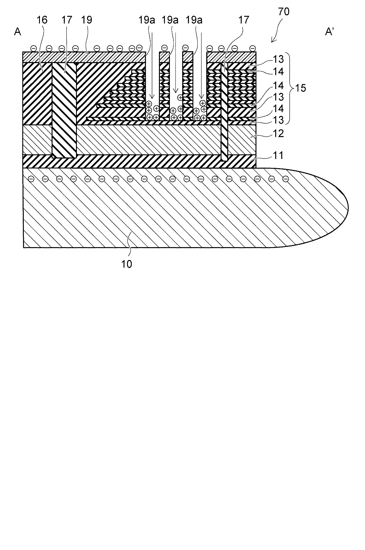
これにより、図5に示すように、レジストパターン19をマスクとして、積層体15がエッチングされる。この結果、積層体15にメモリホールMHが形成される。このとき、シリコンウェーハ10は、電極114により負に帯電し、シリコンウェーハ10の電位Vsは負となる。また、ウェーハ70の表面の電位は、シリコンウェーハ10の電位Vsと等しくなる。なお、図5〜図7においては、陽イオンを「+」を円で囲んだ記号で表し、電子を「−」を円で囲んだ記号で表している。
Thereby, as shown in FIG. 5, the
一方、バイアス電力により、メモリホールMH内には、プラズマ200中の陽イオンが略垂直に引き込まれる。このとき、プラズマ200中の電子も無秩序な運動によりメモリホールMH内に進入するが、電子の進入量は陽イオンの進入量よりも少ない。このため、エッチングの進行に伴い、メモリホールMHの底面は正に帯電し、メモリホールMHの底面の電位Vbは、電位Vsに対して正となる。この結果、シリコンウェーハ10の電位VsとメモリホールMHの底面の電位Vbとの電位差ΔVsbの絶対値|ΔVsb|は、放電時間に依存して増加する。
On the other hand, the bias power draws the cations in the
そこで、本実施形態においては、積層体15におけるメモリホールMHの直下域に配置されたシリコン酸化層13及びシリコン窒化層14を残して第1ステップを終了する。そのため、電位差ΔVsbによって絶縁膜11の絶縁破壊が生じない。すなわち、第1ステップにおいては、メモリホールMHは積層体15を貫通せず、導電部材12には到達しない。但し、第1ステップによって、メモリホールMHの大部分、例えば、積層体15の厚さの半分以上を占める部分を形成する。このため、第1ステップの条件はエッチングレート及び加工形状を重視して決定する。
Therefore, in the present embodiment, the first step is finished while leaving the
次に、図2(a)〜(c)に示す第2ステップを実行する。第2ステップにおいては、第1ステップとは異なり、パルス信号SPの周波数を例えば5kHzとし、デューティ比を例えば25%とする。これにより、パルス信号SPの値がオンであるオン期間Tonの長さは50μsec(マイクロ秒)となり、パルス信号SPの値がオフであるオフ期間Toffの長さは150μsecとなる。そして、交流電力PH、交流電力PL及びパルス信号SPが重畳された重畳波WSが電極114に印加される。なお、図2においては、図示の便宜上、交流電力PLの周期とパルス信号SPの周期がほぼ同じに描かれているが、実際には、交流電力PLの周波数は例えば2MHzであり、パルス信号SPの周期は例えば5kHzであるため、パルス信号SPの周期は交流電力PLの周期の例えば400倍である。後述する図11についても同様である。表2に、第2ステップにおける条件例を示す。
Next, the second step shown in FIGS. 2A to 2C is executed. In the second step, unlike the first step, the frequency of the pulse signal SP is set to 5 kHz and the duty ratio is set to 25%, for example. As a result, the length of the on period Ton in which the value of the pulse signal SP is on is 50 μsec (microseconds), and the length of the off period Toff in which the value of the pulse signal SP is off is 150 μsec. Then, the superimposed wave WS on which the AC power PH, the AC power PL, and the pulse signal SP are superimposed is applied to the
オン期間Tonには、バイアス電力が印加されるため、陽イオンがメモリホールMH内に引き込まれてエッチングが進行すると共に、メモリホールMHの底面に正電荷が蓄積する。一方、オフ期間Toffには、バイアス電力がゼロとなるため、陽イオンがメモリホールMH内に引き込まれなくなる。このため、エッチングはほとんど進行しなくなるが、図6に示すように、メモリホールMH内に蓄積された正電荷がメモリホールMHの外部の負電荷と結合して対消滅し、メモリホールMHの底面における正電荷が減少する。従って、オン期間Tonとオフ期間Toffとを繰り返すことにより、メモリホールMHの底面における正電荷の蓄積を抑制し、電位差ΔVsbの絶対値の増大を抑制しつつ、エッチングを進行させることができる。 Since the bias power is applied during the on period Ton, positive ions are drawn into the memory hole MH and etching progresses, and positive charges are accumulated on the bottom surface of the memory hole MH. On the other hand, during the off period Toff, the bias power becomes zero, so that positive ions are not drawn into the memory hole MH. For this reason, the etching hardly progresses, but as shown in FIG. 6, the positive charges accumulated in the memory hole MH are coupled with the negative charges outside the memory hole MH to be pair annihilated, and the bottom surface of the memory hole MH is erased. The positive charge at is reduced. Therefore, by repeating the on period Ton and the off period Toff, the accumulation of positive charges on the bottom surface of the memory hole MH can be suppressed, and the etching can be advanced while suppressing the increase of the absolute value of the potential difference ΔVsb.
この結果、図7に示すように、積層体15におけるメモリホールMHの直下域に配置された部分において絶縁破壊を生じさせることなく、メモリホールMHを導電部材12まで到達させることができる。このとき、メモリホールMHの底面に蓄積された正電荷が導電部材12に流入し、導電部材12が正に帯電する。一方、シリコンウェーハ10は負に帯電している。従って、絶縁膜11には電圧が印加されるが、上述の第2ステップにおいて、メモリホールMHの底面の正電荷が低減されているため、絶縁膜11に印加される電圧も軽減され、絶縁膜11が絶縁破壊することも抑制できる。積層体15及び絶縁膜11の絶縁破壊をより確実に防止するためには、オン期間Tonを50μsec以下とし、オフ期間Toffを50μsec以上とし、パルス信号SPのデューティ比を50%以下とすることが好ましい。メモリホールMHが導電部材12に確実に到達した時点で、第2ステップを停止し、エッチングを終了する。メモリホールMHの直径は例えば150nm(ナノメートル)以下であり、アスペクト比は5より大きい。
As a result, as shown in FIG. 7, the memory hole MH can reach the
第2ステップにおいては、パルス信号SPのデューティ比が低すぎると、オン期間Tonが短くなるため、エッチング速度が低下して加工が進まないか、又は、メモリホールMHの側面が垂直面から傾斜して加工形状が劣化する。一方、デューティ比が高すぎると、オフ期間Toffが短くなるため、電位差ΔVsbが大きくなり、絶縁破壊が生じる可能性が増加する。このため、パルス信号SPのデューティ比は、エッチング特性の確保と電位差ΔVsbの緩和が両立する範囲内で設定する。 In the second step, if the duty ratio of the pulse signal SP is too low, the ON period Ton becomes short, so the etching rate decreases and the processing does not proceed, or the side surface of the memory hole MH is inclined from the vertical surface. The processed shape deteriorates. On the other hand, if the duty ratio is too high, the off period Toff becomes short, so that the potential difference ΔVsb becomes large and the possibility of dielectric breakdown increases. Therefore, the duty ratio of the pulse signal SP is set within a range in which both the securing of etching characteristics and the relaxation of the potential difference ΔVsb are compatible.
次に、図8に示すように、ドライエッチング装置100からウェーハ70を取り出す。そして、メモリホールMH内に柱状部材20を形成する。以下、この工程及び柱状部材20の構造について、詳細に説明する。
Next, as shown in FIG. 8, the
図9及び図10に示すように、メモリホールMHの底面において、導電部材12を起点としてシリコンをエピタキシャル成長させて、エピタキシャルシリコン部材(図示せず)を形成する。次に、メモリホールMHの内面上にシリコン酸化層33を形成する。次に、シリコン窒化物(SiN)を堆積させて電荷蓄積膜32を形成する。次に、シリコン酸化物、シリコン窒化物及びシリコン酸化物をこの順に堆積させて、シリコン酸化層31c、シリコン窒化層31b及びシリコン酸化層31aを形成することにより、トンネル絶縁膜31を形成する。
As shown in FIGS. 9 and 10, on the bottom surface of the memory hole MH, silicon is epitaxially grown starting from the
次に、シリコンを堆積させてカバーシリコン層(図示せず)を形成し、RIEを施して、カバーシリコン層、トンネル絶縁膜31、電荷蓄積膜32及びシリコン酸化層33を除去して、エピタキシャルシリコン部材を露出させる。次に、シリコンを堆積させて、ボディシリコン層を形成する。ボディシリコン層はエピタキシャルシリコン部材及びトンネル絶縁膜31に接する。カバーシリコン層及びボディシリコン層により、シリコンピラー30が形成される。次に、シリコン酸化物を堆積させることにより、コア部材29を形成する。コア部材29により、メモリホールMHが埋め込まれる。このようにして、柱状部材20が形成される。
Next, silicon is deposited to form a cover silicon layer (not shown), and RIE is performed to remove the cover silicon layer, the
次に、図8に示すように、積層体15にスリット(図示せず)を形成する。スリットは積層体15を貫通する。次に、例えば熱燐酸を用いたウェットエッチングを施すことにより、スリットを介してシリコン窒化層14(図7参照)を除去する。これにより、シリコン酸化層13間にスペースが形成される。
Next, as shown in FIG. 8, slits (not shown) are formed in the
次に、図9及び図10に示すように、スリットを介してアルミニウム酸化物を堆積させて、スペースの内面上にアルミニウム酸化層34を形成する。シリコン酸化層33及びアルミニウム酸化層34により、ブロック絶縁膜35が構成される。トンネル絶縁膜31、電荷蓄積膜32及びブロック絶縁膜35により、メモリ膜36が形成される。
Next, as shown in FIGS. 9 and 10, aluminum oxide is deposited through the slit to form an
次に、スリットを介してチタン窒化物及びチタンを堆積させることにより、アルミニウム酸化層34上にバリアメタル層39を形成する。次に、スリットを介してスペース内にタングステンを堆積させて、本体部38を形成する。次に、エッチングを施すことにより、スリット内からタングステン、チタン、チタン窒化物及びアルミニウム酸化物を除去し、スペース内にのみ残留させる。これにより、スペース内に、本体部38及びバリアメタル層39を含む電極膜40が形成される。このようにして、シリコン窒化層14が電極膜40に置換される。次に、図3に示すように、ダイシングラインDLに沿ってウェーハ70を切断し、複数のチップTpに分断する。このようにして、本実施形態に係る半導体装置1が製造される。
Next, a
次に、本実施形態の効果について説明する。
本実施形態においては、メモリホールMHを形成するためのドライエッチングを、第1ステップと第2ステップに分けて実行している。具体的には、エッチングの開始時からメモリホールMHが積層体15を貫通する直前まで第1ステップを実行し、その後、エッチングの終了まで第2ステップを実行する。
Next, the effect of this embodiment will be described.
In the present embodiment, the dry etching for forming the memory hole MH is performed in the first step and the second step. Specifically, the first step is performed from the start of etching until immediately before the memory hole MH penetrates the stacked
そして、第1ステップの条件は、エッチングレート及び加工形状を重視して決定されている。具体的には、パルス信号SPの値は常にオンとし、交流電力PLを連続的に印加する。これにより、積層体15のエッチングを精度良く効率的に実施することができる。また、第2ステップの条件は、電位差ΔVsbの緩和を考慮して決定されているため、積層体15及び絶縁膜11の絶縁破壊を抑制しつつ、エッチングを終端させることができる。この結果、アスペクト比が高いメモリホールMHを安定して形成することができる。
Then, the conditions of the first step are determined with emphasis on the etching rate and the processed shape. Specifically, the value of the pulse signal SP is always on, and the AC power PL is continuously applied. Thereby, the etching of the stacked
これに対して、仮に、第1ステップのみでメモリホールMHを形成すると、メモリホールMHの底面に正電荷が蓄積されていき、電位差ΔVsbの絶対値は、放電時間に応じて増加する。この結果、メモリホールMHが導電部材12に到達する直前において、絶縁膜11にアーキングが発生し、絶縁破壊される可能性がある。
On the other hand, if the memory hole MH is formed only in the first step, positive charges are accumulated on the bottom surface of the memory hole MH, and the absolute value of the potential difference ΔVsb increases according to the discharge time. As a result, arcing may occur in the insulating
仮に、第1ステップのみでメモリホールMHを形成すると、メモリホールMHの底面に正電荷が蓄積されていき、電位差ΔVsbの絶対値は、放電時間に応じて増加する。この結果、メモリホールMHが導電部材12に到達したときに、メモリホールMHの底面に蓄積された正電荷が導電部材12に注入され、シリコンウェーハ10と導電部材12との間に電圧が発生し、絶縁膜11に電界が印加される。これにより、絶縁膜11にアーキングが発生し、絶縁破壊される可能性がある。
If the memory hole MH is formed only in the first step, positive charges are accumulated on the bottom surface of the memory hole MH, and the absolute value of the potential difference ΔVsb increases according to the discharge time. As a result, when the memory hole MH reaches the
メモリホールMHの底面又は導電部材12に大量の正電荷が蓄積された状態でアーキングが発生すると、絶縁破壊された部分に大電流が流れ、大きなジュール熱が発生する。これにより、電流経路の温度がシリコン酸化物の融点(約1600℃)を超えると、電流経路の周辺の構造体が溶解する。この結果、単なる絶縁破壊よりも大きな部分が破壊されてしまう。
When arcing occurs in the state where a large amount of positive charges are accumulated on the bottom surface of the memory hole MH or the
なお、本実施形態における第1ステップ及び第2ステップの条件は、上述の表1及び表2に記載した例には限定されない。例えば、第1ステップにおいて、パルス信号SPのデューティ比を100%未満とし、交流電力PLが印加されない期間を設けてもよい。但し、この場合、第1ステップにおけるパルス信号SPのデューティ比は第2ステップにおけるパルス信号SPのデューティ比よりも高くし、例えば、50%以上とする。 The conditions of the first step and the second step in the present embodiment are not limited to the examples described in Table 1 and Table 2 above. For example, in the first step, the duty ratio of the pulse signal SP may be set to less than 100%, and a period during which the AC power PL is not applied may be provided. However, in this case, the duty ratio of the pulse signal SP in the first step is set higher than the duty ratio of the pulse signal SP in the second step, for example, 50% or more.
(第2の実施形態)
次に、第2の実施形態について説明する。
図11は、横軸に時間をとり、縦軸に各電力及び信号の値をとって、本実施形態に係るドライエッチング方法を示すタイミングチャートである。
(Second embodiment)
Next, a second embodiment will be described.
FIG. 11 is a timing chart showing the dry etching method according to the present embodiment, in which the horizontal axis represents time and the vertical axis represents values of each power and signal.
図11に示すように、本実施形態に係る半導体装置の製造方法においては、前述の第1の実施形態と比較して、第1ステップと第2ステップとの間に、第3ステップが設けられている点が異なっている。すなわち、本実施形態に係るドライエッチングは、第1ステップ、第3ステップ、第2ステップの順に実行する。本実施形態における第1ステップ及び第2ステップの内容は、それぞれ、第1の実施形態の第1ステップ及び第2ステップの内容と同じである。表3に、第3ステップにおける条件例を示す。 As shown in FIG. 11, in the method of manufacturing a semiconductor device according to this embodiment, a third step is provided between the first step and the second step as compared with the first embodiment described above. Is different. That is, the dry etching according to this embodiment is performed in the order of the first step, the third step, and the second step. The contents of the first step and the second step in the present embodiment are the same as the contents of the first step and the second step in the first embodiment, respectively. Table 3 shows an example of conditions in the third step.
図11及び表3に示すように、第1ステップが終了した後、C4F8ガス及びO2ガスの供給を停止し、アルゴンガス(Ar)の流量を60sccmから200sccmに増加させる。また、低周波電源123が交流電力PL(2MHz)の出力を停止し、高周波電源121が交流電力PH(60MHz)の出力を2000Wから2500Wに増加させる。これにより、第3ステップが開始される。
As shown in FIG. 11 and Table 3, after the first step is completed, the supply of C 4 F 8 gas and O 2 gas is stopped, and the flow rate of argon gas (Ar) is increased from 60 sccm to 200 sccm. Further, the low
第3ステップにおいては、交流電力PLを停止するため、パルス信号SPの値によらず、電極114に交流電力PLは供給されなくなる。従って、パルス信号SPの周波数及びデューティ比は任意である。なお、低周波電源123が交流電力PLを出力したまま、パルス発生器125がパルス信号SPの値を常にオフ、すなわち、任意の周波数でデューティ比を0%としてもよい。一方、交流電力PHを供給し続けることにより、プラズマ200は維持される。しかし、交流電力PLを停止することにより、バイアス電力は印加されなくなり、陽イオンがメモリホールMH内に引き込まれなくなる。
In the third step, since the AC power PL is stopped, the AC power PL is not supplied to the
これにより、図12に示すように、第1ステップにおいてメモリホールMHの底面に蓄積された正電荷が、メモリホールMH外の負電荷と結合して対消滅する。この結果、電位差ΔVsbの絶対値が減少する。このとき、C4F8ガス及びO2ガスの供給を停止することにより、チャンバー本体110内がアルゴンガスに置換される。この結果、C4F8ガス及びO2ガスのラジカル種による等方性エッチングを抑制できる。このようにして、第1ステップにおいてメモリホールMHの底面に蓄積された正電荷の少なくとも一部を、第3ステップにおいて消滅させる。
As a result, as shown in FIG. 12, the positive charges accumulated on the bottom surface of the memory hole MH in the first step are combined with the negative charges outside the memory hole MH to disappear in pairs. As a result, the absolute value of the potential difference ΔVsb decreases. At this time, by stopping the supply of C 4 F 8 gas and O 2 gas, the inside of the
この状態で、第2ステップに移行する。すなわち、図11及び表2に示すように、C4F8ガス及びO2ガスの供給を再開すると共に、アルゴンガスの流量を200sccmから60sccmに減少させる。これにより、プラズマ200中において反応性の陽イオンが増加する。また、交流電力PL(2MHz)の出力を再開し、交流電力PH(60MHz)の出力を2500Wから2000Wに減少させる。そして、周波数が5kHz、デューティ比が25%のパルス信号SPを出力する。これにより、第2ステップが進行し、メモリホールMHの残部が形成される。
In this state, the process proceeds to the second step. That is, as shown in FIG. 11 and Table 2, the supply of the C 4 F 8 gas and the O 2 gas is restarted and the flow rate of the argon gas is reduced from 200 sccm to 60 sccm. As a result, reactive cations increase in the
次に、本実施形態の効果について説明する。
本実施形態においては、第1ステップの後に第3ステップを実行することにより、第1ステップにおいてメモリホールMHの底面に蓄積された正電荷を消失させ、電位差ΔVsbの絶対値を低減する。その後、第2ステップを実行する。これにより、第2ステップにおけるアーキングの発生をより効果的に抑制することができる。また、交流電力PHを増加させることにより、電位差ΔVsbの緩和をより一層促進することができる。
本実施形態における上記以外の方法は、前述の第1の実施形態と同様である。
Next, the effect of this embodiment will be described.
In the present embodiment, by executing the third step after the first step, the positive charge accumulated on the bottom surface of the memory hole MH in the first step is eliminated, and the absolute value of the potential difference ΔVsb is reduced. Then, the second step is executed. Thereby, the occurrence of arcing in the second step can be suppressed more effectively. Further, by increasing the AC power PH, the relaxation of the potential difference ΔVsb can be further promoted.
The method of this embodiment other than the above is the same as that of the above-described first embodiment.
なお、前述の各実施形態においては、積層型の半導体記憶装置1の製造プロセスにおいて、メモリホールを形成する際に、上述のドライエッチング方法を適用する例を示したが、これには限定されない。例えば、半導体記憶装置1の製造プロセスにおいて、層間絶縁膜16に電極膜40に接続するためのコンタクトホールを形成する際に、上述のドライエッチング方法を適用してもよい。また、積層体15にスリットを形成する際に、各実施形態に係るドライエッチング方法を適用してもよい。または、積層型の半導体記憶装置以外の半導体装置の製造プロセスにおいて、ホール又はスリットを形成する際に、各実施形態に係るドライエッチング方法を適用してもよい。
In each of the above-described embodiments, an example in which the above-described dry etching method is applied when the memory hole is formed in the manufacturing process of the stacked semiconductor memory device 1 is shown, but the invention is not limited to this. For example, in the manufacturing process of the semiconductor memory device 1, the above-mentioned dry etching method may be applied when forming a contact hole for connecting to the
より一般的には、第1導電性部材、第1絶縁膜、第2導電性部材及び第2絶縁膜がこの順に積層された構造体であって、第2導電性部材が構造体の表面に露出していない構造体において、第2絶縁膜から第2導電性部材にかけて、イオン種を用いて、ホール又はスリット等の開口部を形成する場合に、前述の各実施形態を適用すれば、第2絶縁膜及び第1絶縁膜におけるアーキングを抑制することができる。また、エッチングの対象となる構造体には、第2導電性部材の電荷を逃がす避雷針のような構造を設ける場合もあるが、このような構造体についても、前述の各実施形態を適用することができる。但し、前述の各実施形態は、このような構造が設けられていない構造体をエッチングする場合に、特に有効である。 More generally, it is a structure in which a first conductive member, a first insulating film, a second conductive member and a second insulating film are laminated in this order, and the second conductive member is on the surface of the structure. In the structure that is not exposed, when the openings such as holes or slits are formed using the ionic species from the second insulating film to the second conductive member, if each of the above-described embodiments is applied, Arcing in the second insulating film and the first insulating film can be suppressed. Further, the structure to be etched may be provided with a structure such as a lightning rod that allows the charges of the second conductive member to escape, and the above-described embodiments are also applied to such a structure. You can However, each of the above-described embodiments is particularly effective when etching a structure having no such structure.
仮に、第2ステップを実行せず、第1ステップのみでホール又はスリットを形成しようとすると、ホールの直径又はスリットの幅が150nm以下であり、アスペクト比が5よりも大きい場合に、アーキングの発生が顕著となる。このため、このような加工において、前述の各実施形態の効果が特に大きい。 If the hole or slit is formed only in the first step without executing the second step, arcing occurs when the diameter of the hole or the width of the slit is 150 nm or less and the aspect ratio is larger than 5. Becomes noticeable. Therefore, in such processing, the effects of the above-described embodiments are particularly large.
また、前述の各実施形態においては、スイッチ126を用いて、第2ステップのオン期間Tonでは交流電力PLを出力し、オフ期間Toffでは交流電力PLを出力しない例を示したが、これには限定されない。例えば、スイッチ126の代わりにフィルタ等の出力変調器を設け、オフ期間Toffには微弱な交流電力PLを出力してもよい。オフ期間Toffにおける交流電力PLの出力が、オン期間Tonにおける交流電力PLの出力に対して十分に小さければ、交流電力PLを遮断した場合と実質的に同等な効果を得ることができる。
In each of the above-described embodiments, the example in which the
(試験例1)
次に、試験例について説明する。
図13は、横軸に時間をとり、縦軸に各電位をとって、本試験例におけるサンプル各部の電位変化を示すグラフ図である。
図14は、横軸に時間をとり、縦軸に電位差ΔVsbの絶対値をとって、本試験例におけるオン期間Ton及びオフ期間Toffの電位差ΔVsbの変化を示すグラフ図である。
(Test Example 1)
Next, a test example will be described.
FIG. 13 is a graph showing the potential change of each part of the sample in this test example, where the horizontal axis represents time and the vertical axis represents each potential.
FIG. 14 is a graph showing changes in the potential difference ΔVsb in the on period Ton and the off period Toff in this test example, with the horizontal axis representing time and the vertical axis representing the absolute value of the potential difference ΔVsb.
本試験例においては、前述の第1の実施形態のウェーハ70と同様なサンプルを作製し、第2ステップと同様なエッチングを行い、シリコンウェーハ10の表面の電位Vs、及び、メモリホールMHの底面の電位Vbを測定した。
In this test example, a sample similar to the
その結果、図13に示すように、初期状態における電位Vs及び電位Vbは共に0Vであり、従って、電位差ΔVsbも0Vであった。その後、バイアス電力がオンとなるオン期間Tonが進行すると、電位Vs及び電位Vbが共に負となり、その絶対値が増加した。このとき、電位Vsの絶対値の増加率は電位Vbの絶対値の増加率よりも大きくなり、従って、電位差ΔVsbの絶対値も増加した。次に、バイアス電力がオフとなるオフ期間Toffになると、電位Vs及び電位Vbの値は負のまま、その絶対値が減少した。このとき、電位Vsの絶対値の減少率は電位Vbの絶対値の減少率よりも大きく、電位Vsと電位Vbはほぼ等しくなった。従って、電位差ΔVsbの絶対値は減少し、0に収束した。なお、図13に実線で示すように、オン期間Tonを続行すると、電位Vsは一定値に収束し、電位Vbの絶対値の減少に伴って、電位差ΔVsbの絶対値は増加した。 As a result, as shown in FIG. 13, both the potential Vs and the potential Vb in the initial state were 0V, and therefore the potential difference ΔVsb was also 0V. After that, when the on period Ton in which the bias power is turned on progresses, both the potential Vs and the potential Vb become negative, and the absolute value thereof increases. At this time, the increase rate of the absolute value of the potential Vs was larger than the increase rate of the absolute value of the potential Vb, and thus the absolute value of the potential difference ΔVsb also increased. Next, in the off period Toff in which the bias power was turned off, the absolute values of the potential Vs and the potential Vb remained negative while decreasing their absolute values. At this time, the rate of decrease of the absolute value of the potential Vs was larger than the rate of decrease of the absolute value of the potential Vb, and the potential Vs and the potential Vb were almost equal. Therefore, the absolute value of the potential difference ΔVsb decreased and converged to zero. As indicated by the solid line in FIG. 13, when the on period Ton is continued, the potential Vs converges to a constant value, and the absolute value of the potential difference ΔVsb increases as the absolute value of the potential Vb decreases.
また、オン期間Tonを50μsecよりも長くすると、アーキングが発生した。第2ステップにおいて、バイアス電力を印加し続けると、1枚のウェーハ70に数百ないし数千ヶ所のアーキングが発生した。このため、オン期間Tonは50μsec以下とすることが好ましい。
When the ON period Ton is longer than 50 μsec, arcing occurs. In the second step, when the bias power was continuously applied, arcing occurred in several hundreds to several thousands on one
図14に示すように、オン期間Tonを50μsecとし、その後、オフ期間Toffを進行させると、オフ期間Toffが50μsec経過した時点で、ΔVsbがほぼ0となった。このため、オフ期間Toffは50μsec以上とすることが好ましい。 As shown in FIG. 14, when the on period Ton was set to 50 μsec and then the off period Toff was advanced, ΔVsb became almost 0 when the off period Toff passed 50 μsec. Therefore, the off period Toff is preferably set to 50 μsec or more.
(試験例2)
次に、試練例2について説明する。
本試験例においては、プラズマシミュレーションを行い、バイアス電力がオンの場合と、バイアス電力がオフの場合において、メモリホールMHの底面及びメモリホールMHの開口部付近について、陽イオンのフラックス及び電子のフラックスを算出した。その結果、バイアス電力がオンのとき、メモリホールMHの底面においては、陽イオンのフラックスが電子のフラックスより多く、間口部付近においては、底面と比較して、陽イオンのフラックスと電子のフラックスとの差が小さかった。このため、メモリホールMHの底面における陽イオンの蓄積に起因して、底面と開口部付近との間で電位差が発生することが、また、メモリホールMHの開口部付近とシリコンウェーハ10とは、ウェーハ70の外面を介して導通されているため、電位差ΔVsbが生じることが確認された。
(Test Example 2)
Next, trial example 2 will be described.
In this test example, a plasma simulation is performed, and when the bias power is on and when the bias power is off, the cation flux and the electron flux are measured around the bottom surface of the memory hole MH and the opening of the memory hole MH. Was calculated. As a result, when the bias power is on, the flux of cations is larger than the flux of electrons at the bottom surface of the memory hole MH, and the flux of cations and the flux of electrons are nearer to the bottom surface in the vicinity of the frontage. The difference was small. Therefore, a potential difference may occur between the bottom surface and the vicinity of the opening due to the accumulation of cations on the bottom surface of the memory hole MH. Further, between the vicinity of the opening of the memory hole MH and the
以上説明した実施形態によれば、アスペクト比が高い開口部を安定して形成することができるドライエッチング方法及び半導体装置の製造方法を実現することができる。 According to the embodiments described above, it is possible to realize a dry etching method and a semiconductor device manufacturing method that can stably form an opening having a high aspect ratio.
以上、本発明のいくつかの実施形態を説明したが、これらの実施形態は、例として提示したものであり、発明の範囲を限定することは意図していない。これら新規な実施形態は、その他の様々な形態で実施されることが可能であり、発明の要旨を逸脱しない範囲で、種々の省略、置き換え、変更を行うことができる。これら実施形態やその変形は、発明の範囲や要旨に含まれるとともに、特許請求の範囲に記載された発明及びその等価物の範囲に含まれる。 Although some embodiments of the present invention have been described above, these embodiments are presented as examples and are not intended to limit the scope of the invention. These novel embodiments can be implemented in various other forms, and various omissions, replacements, and changes can be made without departing from the spirit of the invention. These embodiments and modifications thereof are included in the scope and gist of the invention, and are also included in the scope of the invention described in the claims and the equivalents thereof.
1:半導体装置、10:シリコンウェーハ、11:絶縁膜、12:導電部材、13:シリコン酸化層、14:シリコン窒化層、15:積層体、16:層間絶縁膜、17:絶縁部材、19:レジストパターン、19a:開口部、20:柱状部材、29:コア部材、30:シリコンピラー、31:トンネル絶縁膜、31a:シリコン酸化層、31b:シリコン窒化層、31c:シリコン酸化層、32:電荷蓄積膜、33:シリコン酸化層、34:アルミニウム酸化層、35:ブロック絶縁膜、36:メモリ膜、38:本体部、39:バリアメタル層、40:電極膜、70:ウェーハ、100:ドライエッチング装置、101:チャンバー、102:電源部、110:チャンバー本体、111:ガス導入管、112:ガス排出管、113:ポンプ、114:電極、115:対向電極、121:高周波電源、122:整合器、123:低周波電源、124:整合器、125:パルス発生器、126:スイッチ、DL:ダイシングライン、MH:メモリホール、PH:交流電力、PL:交流電力、SP:パルス信号、Toff:オフ期間、Ton:オン期間、Tp:チップ、Vb:メモリホール底面の電位、Vs:シリコンウェーハの電位、WS:重畳波、ΔVsb:電位差 1: semiconductor device, 10: silicon wafer, 11: insulating film, 12: conductive member, 13: silicon oxide layer, 14: silicon nitride layer, 15: laminated body, 16: interlayer insulating film, 17: insulating member, 19: Resist pattern, 19a: opening, 20: columnar member, 29: core member, 30: silicon pillar, 31: tunnel insulating film, 31a: silicon oxide layer, 31b: silicon nitride layer, 31c: silicon oxide layer, 32: charge Storage film, 33: Silicon oxide layer, 34: Aluminum oxide layer, 35: Block insulating film, 36: Memory film, 38: Main body part, 39: Barrier metal layer, 40: Electrode film, 70: Wafer, 100: Dry etching Device, 101: Chamber, 102: Power supply part, 110: Chamber body, 111: Gas introduction pipe, 112: Gas discharge pipe, 113: Pump, 114: Electrode, 115: Counter electrode, 121: High frequency power supply, 122: Matching device , 123: low frequency power supply, 124: matching unit, 125: pulse generator, 126: switch, DL: dicing line, MH: memory hole, PH: AC power, PL: AC power, SP: pulse signal, Toff: OFF. Period, Ton: ON period, Tp: chip, Vb: potential of bottom surface of memory hole, Vs: potential of silicon wafer, WS: superimposed wave, ΔVsb: potential difference
Claims (10)
前記第1工程の前に、イオン種を用いてバイアス電力を印加しながら前記第2導電性部材を露出させないように前記第2絶縁膜をエッチングする第2工程と、
を備え、
前記第1工程において、前記バイアス電力を連続して印加する時間を50マイクロ秒以下とし、前記バイアス電力のデューティ比を50%以下とし、
前記第2工程において、前記バイアス電力は継続的に印加するか、前記第1工程よりも高いデューティ比で断続的に印加するドライエッチング方法。 A first conductive member, a first insulating film provided on the first conductive member, a second conductive member provided on the first insulating film, and provided on the second conductive member. A second step of exposing the second conductive member by etching the second insulating film while applying bias power intermittently to the workpiece including the second insulating film using an ion species ; ,
Before the first step, a second step of etching the second insulating film so as to prevent the second conductive member from being exposed while applying bias power using an ionic species;
Equipped with
In the first step, the time for continuously applying the bias power is set to 50 microseconds or less, and the duty ratio of the bias power is set to 50% or less ,
In the second step, the dry etching method in which the bias power is continuously applied or intermittently applied with a higher duty ratio than in the first step .
前記第1工程の前に、イオン種を用いてバイアス電力を印加しながら前記第2導電性部材を露出させないように前記第2絶縁膜をエッチングする第2工程と、
前記第2工程の後、前記第1工程の前に、バイアス電力を印加しない第3工程と、
を備え、
前記第1工程において、前記バイアス電力を連続して印加する時間を50マイクロ秒以下とし、前記バイアス電力のデューティ比を50%以下とするドライエッチング方法。 A first conductive member, a first insulating film provided on the first conductive member, a second conductive member provided on the first insulating film, and provided on the second conductive member. A second step of exposing the second conductive member by etching the second insulating film while applying bias power intermittently to the workpiece including the second insulating film using an ion species ; ,
Before the first step, a second step of etching the second insulating film so as to prevent the second conductive member from being exposed while applying bias power using an ionic species;
After the second step and before the first step, a third step in which no bias power is applied,
Equipped with
In the first step, a dry etching method in which the time for continuously applying the bias power is 50 microseconds or less and the duty ratio of the bias power is 50% or less.
前記第1工程の前に、イオン種を用いてバイアス電力を印加しながら前記第2導電性部材を露出させないように前記第2絶縁膜をエッチングする第2工程と、
を備え、
前記第1工程において、前記バイアス電力を連続して印加する時間を50マイクロ秒以下とし、前記バイアス電力のデューティ比を50%以下とし、
前記第2工程において、前記バイアス電力は継続的に印加するか、前記第1工程よりも高いデューティ比で断続的に印加する半導体装置の製造方法。 A first conductive member, a first insulating film provided on the first conductive member, a second conductive member provided on the first insulating film, and provided on the second conductive member. the workpiece including the second insulating film, by etching the second insulating film while intermittently applied bias power using an ion species, a first step of exposing the second conductive member ,
Before the first step, a second step of etching the second insulating film so as to not expose the second conductive member while applying bias power using ionic species;
Equipped with
In the first step, the time for continuously applying the bias power is 50 microseconds or less, and the duty ratio of the bias power is 50% or less ,
In the second step, the method of manufacturing a semiconductor device , wherein the bias power is applied continuously or intermittently at a duty ratio higher than that in the first step .
前記第1工程の前に、イオン種を用いてバイアス電力を印加しながら前記第2導電性部材を露出させないように前記第2絶縁膜をエッチングする第2工程と、
前記第2工程の後、前記第1工程の前に、バイアス電力を印加しない第3工程と、
を備え、
前記第1工程において、前記バイアス電力を連続して印加する時間を50マイクロ秒以下とし、前記バイアス電力のデューティ比を50%以下とする半導体装置の製造方法。 A first conductive member, a first insulating film provided on the first conductive member, a second conductive member provided on the first insulating film, and provided on the second conductive member. A second step of exposing the second conductive member by etching the second insulating film while applying bias power intermittently to the workpiece including the second insulating film using an ion species ; ,
Before the first step, a second step of etching the second insulating film so as to prevent the second conductive member from being exposed while applying bias power using an ionic species;
After the second step and before the first step, a third step in which no bias power is applied,
Equipped with
In the first step, a method of manufacturing a semiconductor device, wherein a time for continuously applying the bias power is 50 microseconds or less and a duty ratio of the bias power is 50% or less.
Priority Applications (2)
| Application Number | Priority Date | Filing Date | Title |
|---|---|---|---|
| JP2016226298A JP6697372B2 (en) | 2016-11-21 | 2016-11-21 | Dry etching method and semiconductor device manufacturing method |
| US15/661,243 US10332906B2 (en) | 2016-11-21 | 2017-07-27 | Dry etching method and method for manufacturing semiconductor device |
Applications Claiming Priority (1)
| Application Number | Priority Date | Filing Date | Title |
|---|---|---|---|
| JP2016226298A JP6697372B2 (en) | 2016-11-21 | 2016-11-21 | Dry etching method and semiconductor device manufacturing method |
Publications (2)
| Publication Number | Publication Date |
|---|---|
| JP2018085389A JP2018085389A (en) | 2018-05-31 |
| JP6697372B2 true JP6697372B2 (en) | 2020-05-20 |
Family
ID=62147239
Family Applications (1)
| Application Number | Title | Priority Date | Filing Date |
|---|---|---|---|
| JP2016226298A Active JP6697372B2 (en) | 2016-11-21 | 2016-11-21 | Dry etching method and semiconductor device manufacturing method |
Country Status (2)
| Country | Link |
|---|---|
| US (1) | US10332906B2 (en) |
| JP (1) | JP6697372B2 (en) |
Families Citing this family (7)
| Publication number | Priority date | Publication date | Assignee | Title |
|---|---|---|---|---|
| KR20190132151A (en) * | 2018-05-18 | 2019-11-27 | 에스케이하이닉스 주식회사 | Blank phase shift photomask, phase shift photomask using the blank phase shift photomask, and method of fabricating the phase shift photomask using the blank phase shift photomask |
| JP6846387B2 (en) * | 2018-06-22 | 2021-03-24 | 東京エレクトロン株式会社 | Plasma processing method and plasma processing equipment |
| KR20230048459A (en) * | 2018-06-22 | 2023-04-11 | 도쿄엘렉트론가부시키가이샤 | Control method and plasma treatment device |
| JP7250663B2 (en) * | 2018-12-19 | 2023-04-03 | 東京エレクトロン株式会社 | Plasma processing apparatus and impedance matching method |
| WO2020145051A1 (en) * | 2019-01-09 | 2020-07-16 | 東京エレクトロン株式会社 | Plasma treatment device and plasma treatment method |
| CN116844934A (en) * | 2019-02-05 | 2023-10-03 | 东京毅力科创株式会社 | Plasma processing apparatus |
| US11495470B1 (en) * | 2021-04-16 | 2022-11-08 | Applied Materials, Inc. | Method of enhancing etching selectivity using a pulsed plasma |
Family Cites Families (19)
| Publication number | Priority date | Publication date | Assignee | Title |
|---|---|---|---|---|
| JPH0497523A (en) * | 1990-08-15 | 1992-03-30 | Nec Corp | Manufacture of semiconductor device |
| US5352324A (en) | 1992-11-05 | 1994-10-04 | Hitachi, Ltd. | Etching method and etching apparatus therefor |
| JPH08130205A (en) * | 1994-10-31 | 1996-05-21 | Nippon Steel Corp | Equipment for detecting etching end point of conducting film |
| JPH11219938A (en) | 1998-02-02 | 1999-08-10 | Matsushita Electron Corp | Plasma etching method |
| JP2000091325A (en) * | 1998-09-11 | 2000-03-31 | Hitachi Ltd | Method and device for surface treatment |
| US6492277B1 (en) | 1999-09-10 | 2002-12-10 | Hitachi, Ltd. | Specimen surface processing method and apparatus |
| KR100514150B1 (en) | 1998-11-04 | 2005-09-13 | 서페이스 테크놀로지 시스템스 피엘씨 | A method and apparatus for etching a substrate |
| US6759339B1 (en) * | 2002-12-13 | 2004-07-06 | Silicon Magnetic Systems | Method for plasma etching a microelectronic topography using a pulse bias power |
| US7718538B2 (en) | 2007-02-21 | 2010-05-18 | Applied Materials, Inc. | Pulsed-plasma system with pulsed sample bias for etching semiconductor substrates |
| JP5514413B2 (en) | 2007-08-17 | 2014-06-04 | 東京エレクトロン株式会社 | Plasma etching method |
| KR100919342B1 (en) * | 2007-09-06 | 2009-09-25 | 주식회사 하이닉스반도체 | Method of manufacturing a semiconductor device |
| US8110881B2 (en) * | 2007-09-27 | 2012-02-07 | Taiwan Semiconductor Manufacturing Co., Ltd. | MRAM cell structure with a blocking layer for avoiding short circuits |
| US8154209B2 (en) * | 2009-04-06 | 2012-04-10 | Lam Research Corporation | Modulated multi-frequency processing method |
| KR101328800B1 (en) * | 2011-09-08 | 2013-11-13 | 성균관대학교산학협력단 | Characteristic controlling method of pulsed plasma using Multi-frequency RF pulsed power |
| US9384992B2 (en) * | 2012-02-09 | 2016-07-05 | Tokyo Electron Limited | Plasma processing method |
| JP5968130B2 (en) * | 2012-07-10 | 2016-08-10 | 東京エレクトロン株式会社 | Plasma processing method and plasma processing apparatus |
| JP2014187231A (en) | 2013-03-25 | 2014-10-02 | Tokyo Electron Ltd | Plasma etching method, and plasma etching apparatus |
| JP2014216331A (en) * | 2013-04-22 | 2014-11-17 | 株式会社日立ハイテクノロジーズ | Plasma etching method |
| JP6410592B2 (en) * | 2014-12-18 | 2018-10-24 | 東京エレクトロン株式会社 | Plasma etching method |
-
2016
- 2016-11-21 JP JP2016226298A patent/JP6697372B2/en active Active
-
2017
- 2017-07-27 US US15/661,243 patent/US10332906B2/en active Active
Also Published As
| Publication number | Publication date |
|---|---|
| US20180145086A1 (en) | 2018-05-24 |
| US10332906B2 (en) | 2019-06-25 |
| JP2018085389A (en) | 2018-05-31 |
Similar Documents
| Publication | Publication Date | Title |
|---|---|---|
| JP6697372B2 (en) | Dry etching method and semiconductor device manufacturing method | |
| KR100389642B1 (en) | Surface Treatment Method and Surface Treatment Equipment | |
| US10755895B2 (en) | Ion energy control by RF pulse shape | |
| TWI673752B (en) | Plasma apparatus | |
| US9230824B2 (en) | Method of manufacturing semiconductor device | |
| CN106653532B (en) | Method and system for carrying out advanced ionic control to etch process | |
| US20100213172A1 (en) | Using Positive DC Offset of Bias RF to Neutralize Charge Build-Up of Etch Features | |
| US20110223750A1 (en) | Method for manufacturing semiconductor device and semiconductor manufacturing apparatus | |
| US20180053661A1 (en) | Plasma etching apparatus and method of manufacturing a semiconductor device using the same | |
| KR20220061195A (en) | Broadband plasma processing systems and methods | |
| US20120302065A1 (en) | Pulse-plasma etching method and pulse-plasma etching apparatus | |
| KR20170054280A (en) | Methods and systems for plasma etching using bi-modal process gas composition responsive to plasma power level | |
| JP2000294540A (en) | Manufacture of semiconductor device and apparatus for manufacturing | |
| TWI466161B (en) | Plasma etching method for preparinghigh-aspect-ratio structures and method for preparing stacked capacitors | |
| KR102550393B1 (en) | Plasma processing apparatus and method of fabricating semiconductor device using the same | |
| JP2020031190A5 (en) | ||
| JP2002009043A (en) | Etching device and manufacturing method of semiconductor device using it | |
| CN109216147B (en) | Semiconductor manufacturing apparatus and method of operating the same | |
| KR100305134B1 (en) | Etching method | |
| JP5961794B2 (en) | Method for manufacturing silicon substrate having concavo-convex structure with high aspect ratio | |
| KR20170093303A (en) | Method for Plasma etching and method of fabricating semiconductor using the same | |
| JP2007214588A (en) | Method for fabricating semiconductor device | |
| KR20160011163A (en) | Method for increasing oxide etch selectivity | |
| JPS63288021A (en) | Method and device for plasma processing | |
| KR102448630B1 (en) | METHOD FOR FABRICATING TRENCH IN SiC SEMICONDUCTOR PROCESS |
Legal Events
| Date | Code | Title | Description |
|---|---|---|---|
| A711 | Notification of change in applicant |
Free format text: JAPANESE INTERMEDIATE CODE: A712 Effective date: 20170620 |
|
| A711 | Notification of change in applicant |
Free format text: JAPANESE INTERMEDIATE CODE: A712 Effective date: 20180905 |
|
| A621 | Written request for application examination |
Free format text: JAPANESE INTERMEDIATE CODE: A621 Effective date: 20190314 |
|
| A131 | Notification of reasons for refusal |
Free format text: JAPANESE INTERMEDIATE CODE: A131 Effective date: 20200107 |
|
| A977 | Report on retrieval |
Free format text: JAPANESE INTERMEDIATE CODE: A971007 Effective date: 20191226 |
|
| A521 | Request for written amendment filed |
Free format text: JAPANESE INTERMEDIATE CODE: A523 Effective date: 20200226 |
|
| TRDD | Decision of grant or rejection written | ||
| A01 | Written decision to grant a patent or to grant a registration (utility model) |
Free format text: JAPANESE INTERMEDIATE CODE: A01 Effective date: 20200403 |
|
| A61 | First payment of annual fees (during grant procedure) |
Free format text: JAPANESE INTERMEDIATE CODE: A61 Effective date: 20200424 |
|
| R150 | Certificate of patent or registration of utility model |
Ref document number: 6697372 Country of ref document: JP Free format text: JAPANESE INTERMEDIATE CODE: R150 |