WO2020145051A1 - Plasma treatment device and plasma treatment method - Google Patents

Plasma treatment device and plasma treatment method Download PDF

Info

Publication number
WO2020145051A1
WO2020145051A1 PCT/JP2019/049499 JP2019049499W WO2020145051A1 WO 2020145051 A1 WO2020145051 A1 WO 2020145051A1 JP 2019049499 W JP2019049499 W JP 2019049499W WO 2020145051 A1 WO2020145051 A1 WO 2020145051A1
Authority
WO
WIPO (PCT)
Prior art keywords
frequency power
high frequency
period
lower electrode
plasma processing
Prior art date
Application number
PCT/JP2019/049499
Other languages
French (fr)
Japanese (ja)
Inventor
輿水 地塩
紳治 久保田
Original Assignee
東京エレクトロン株式会社
Priority date (The priority date is an assumption and is not a legal conclusion. Google has not performed a legal analysis and makes no representation as to the accuracy of the date listed.)
Filing date
Publication date
Application filed by 東京エレクトロン株式会社 filed Critical 東京エレクトロン株式会社
Priority to SG11202107162UA priority Critical patent/SG11202107162UA/en
Priority to KR1020217023745A priority patent/KR20210111269A/en
Priority to US17/421,001 priority patent/US20220084787A1/en
Priority to JP2020565660A priority patent/JP7297795B2/en
Priority to CN201980087489.1A priority patent/CN113228830B/en
Publication of WO2020145051A1 publication Critical patent/WO2020145051A1/en
Priority to JP2023097775A priority patent/JP7519507B2/en
Priority to JP2024109623A priority patent/JP2024133658A/en

Links

Images

Classifications

    • HELECTRICITY
    • H01ELECTRIC ELEMENTS
    • H01JELECTRIC DISCHARGE TUBES OR DISCHARGE LAMPS
    • H01J37/00Discharge tubes with provision for introducing objects or material to be exposed to the discharge, e.g. for the purpose of examination or processing thereof
    • H01J37/32Gas-filled discharge tubes
    • H01J37/32009Arrangements for generation of plasma specially adapted for examination or treatment of objects, e.g. plasma sources
    • H01J37/32082Radio frequency generated discharge
    • H01J37/32137Radio frequency generated discharge controlling of the discharge by modulation of energy
    • H01J37/32146Amplitude modulation, includes pulsing
    • HELECTRICITY
    • H01ELECTRIC ELEMENTS
    • H01JELECTRIC DISCHARGE TUBES OR DISCHARGE LAMPS
    • H01J37/00Discharge tubes with provision for introducing objects or material to be exposed to the discharge, e.g. for the purpose of examination or processing thereof
    • H01J37/32Gas-filled discharge tubes
    • H01J37/32009Arrangements for generation of plasma specially adapted for examination or treatment of objects, e.g. plasma sources
    • H01J37/32082Radio frequency generated discharge
    • H01J37/32091Radio frequency generated discharge the radio frequency energy being capacitively coupled to the plasma
    • HELECTRICITY
    • H01ELECTRIC ELEMENTS
    • H01JELECTRIC DISCHARGE TUBES OR DISCHARGE LAMPS
    • H01J37/00Discharge tubes with provision for introducing objects or material to be exposed to the discharge, e.g. for the purpose of examination or processing thereof
    • H01J37/32Gas-filled discharge tubes
    • H01J37/32009Arrangements for generation of plasma specially adapted for examination or treatment of objects, e.g. plasma sources
    • H01J37/32082Radio frequency generated discharge
    • H01J37/32137Radio frequency generated discharge controlling of the discharge by modulation of energy
    • HELECTRICITY
    • H01ELECTRIC ELEMENTS
    • H01JELECTRIC DISCHARGE TUBES OR DISCHARGE LAMPS
    • H01J37/00Discharge tubes with provision for introducing objects or material to be exposed to the discharge, e.g. for the purpose of examination or processing thereof
    • H01J37/32Gas-filled discharge tubes
    • H01J37/32009Arrangements for generation of plasma specially adapted for examination or treatment of objects, e.g. plasma sources
    • H01J37/32082Radio frequency generated discharge
    • H01J37/32174Circuits specially adapted for controlling the RF discharge
    • HELECTRICITY
    • H01ELECTRIC ELEMENTS
    • H01JELECTRIC DISCHARGE TUBES OR DISCHARGE LAMPS
    • H01J37/00Discharge tubes with provision for introducing objects or material to be exposed to the discharge, e.g. for the purpose of examination or processing thereof
    • H01J37/32Gas-filled discharge tubes
    • H01J37/32431Constructional details of the reactor
    • H01J37/32532Electrodes
    • HELECTRICITY
    • H01ELECTRIC ELEMENTS
    • H01LSEMICONDUCTOR DEVICES NOT COVERED BY CLASS H10
    • H01L21/00Processes or apparatus adapted for the manufacture or treatment of semiconductor or solid state devices or of parts thereof
    • H01L21/02Manufacture or treatment of semiconductor devices or of parts thereof
    • H01L21/04Manufacture or treatment of semiconductor devices or of parts thereof the devices having potential barriers, e.g. a PN junction, depletion layer or carrier concentration layer
    • H01L21/18Manufacture or treatment of semiconductor devices or of parts thereof the devices having potential barriers, e.g. a PN junction, depletion layer or carrier concentration layer the devices having semiconductor bodies comprising elements of Group IV of the Periodic Table or AIIIBV compounds with or without impurities, e.g. doping materials
    • H01L21/30Treatment of semiconductor bodies using processes or apparatus not provided for in groups H01L21/20 - H01L21/26
    • H01L21/302Treatment of semiconductor bodies using processes or apparatus not provided for in groups H01L21/20 - H01L21/26 to change their surface-physical characteristics or shape, e.g. etching, polishing, cutting
    • H01L21/306Chemical or electrical treatment, e.g. electrolytic etching
    • H01L21/3065Plasma etching; Reactive-ion etching
    • HELECTRICITY
    • H05ELECTRIC TECHNIQUES NOT OTHERWISE PROVIDED FOR
    • H05HPLASMA TECHNIQUE; PRODUCTION OF ACCELERATED ELECTRICALLY-CHARGED PARTICLES OR OF NEUTRONS; PRODUCTION OR ACCELERATION OF NEUTRAL MOLECULAR OR ATOMIC BEAMS
    • H05H1/00Generating plasma; Handling plasma
    • H05H1/24Generating plasma
    • H05H1/46Generating plasma using applied electromagnetic fields, e.g. high frequency or microwave energy
    • HELECTRICITY
    • H01ELECTRIC ELEMENTS
    • H01JELECTRIC DISCHARGE TUBES OR DISCHARGE LAMPS
    • H01J37/00Discharge tubes with provision for introducing objects or material to be exposed to the discharge, e.g. for the purpose of examination or processing thereof
    • H01J37/32Gas-filled discharge tubes
    • H01J37/32431Constructional details of the reactor
    • H01J37/32715Workpiece holder

Definitions

  • the exemplary embodiments of the present disclosure relate to a plasma processing apparatus and a plasma processing method.
  • Patent Document 1 describes a type of plasma processing apparatus.
  • the plasma processing apparatus described in Patent Document 1 includes a chamber, an electrode, a high frequency power supply, and a high frequency bias power supply.
  • the electrode is provided in the chamber.
  • the substrate is placed on the electrode.
  • the high frequency power supply supplies a pulse of high frequency power to form a high frequency electric field in the chamber.
  • the high frequency bias power supply supplies a pulse of high frequency bias power to the electrodes.
  • the present disclosure provides a technique for controlling the energy of ions supplied from a plasma to a substrate.
  • a plasma processing apparatus in one exemplary embodiment, includes a chamber, a substrate support, a high frequency power supply, a bias power supply, and a controller.
  • the substrate support has a lower electrode and an electrostatic chuck.
  • the electrostatic chuck is provided on the lower electrode.
  • the substrate support is configured to support a substrate mounted thereon within the chamber.
  • the high frequency power source is configured to generate high frequency power supplied to generate plasma from the gas in the chamber.
  • the high frequency power has a first frequency.
  • the bias power supply is electrically connected to the lower electrode.
  • the bias power supply is configured to periodically apply a pulsed negative DC voltage to the lower electrode at a cycle defined by the second frequency.
  • the second frequency is lower than the first frequency.
  • the control unit is configured to control the high frequency power supply.
  • the control unit controls the high frequency power supply to supply the high frequency power within the first partial period of the cycle.
  • the control unit controls the high frequency power supply so that the power level of the high frequency power in the second partial period in the cycle is set to the power level reduced from the power level of the high frequency power in the first partial period.
  • a technique for controlling the energy of ions supplied from a plasma to a substrate is provided.
  • FIGS. 8A and 8B are timing charts of pulsed negative DC voltage according to still another example.
  • 3 is a flowchart illustrating a plasma processing method according to an exemplary embodiment.
  • a plasma processing apparatus in one exemplary embodiment, includes a chamber, a substrate support, a high frequency power supply, a bias power supply, and a controller.
  • the substrate support has a lower electrode and an electrostatic chuck.
  • the electrostatic chuck is provided on the lower electrode.
  • the substrate support is configured to support a substrate mounted thereon within the chamber.
  • the high frequency power source is configured to generate high frequency power supplied to generate plasma from the gas in the chamber.
  • the high frequency power has a first frequency.
  • the bias power supply is electrically connected to the lower electrode.
  • the bias power supply is configured to periodically apply a pulsed negative DC voltage to the lower electrode at a cycle defined by the second frequency.
  • the second frequency is lower than the first frequency.
  • the control unit is configured to control the high frequency power supply.
  • the control unit controls the high frequency power supply so as to supply the high frequency power within the first partial period of the cycle.
  • the control unit controls the high frequency power source so as to set the power level of the high frequency power in the second partial period in the cycle to a power level reduced from the power level of the high frequency power in the first partial period.
  • the pulsed negative DC voltage is periodically supplied to the lower electrode at a cycle defined by the second frequency (hereinafter, referred to as “pulse cycle”).
  • the potential of the substrate changes within the pulse period.
  • high frequency power having a power level higher than that of the high frequency power in the second partial period within the pulse period is supplied. Therefore, the energy of the ions supplied to the substrate depends on the setting of the time range of each of the first partial period and the second partial period within the pulse period. Therefore, according to the above embodiment, it is possible to control the energy of the ions supplied from the plasma to the substrate.
  • the first partial period may be a period in which a pulsed negative DC voltage is applied to the lower electrode.
  • the second partial period may be a period during which the pulsed negative DC voltage is not applied to the lower electrode. According to this embodiment, ions having a relatively high energy can be supplied to the substrate.
  • the first partial period may be a period in which a pulsed negative DC voltage is not applied to the lower electrode.
  • the second partial period may be a period in which a pulsed negative DC voltage is applied to the lower electrode. According to this embodiment, ions having a relatively low energy can be provided to the substrate.
  • control unit may control the high frequency power supply so as to stop the supply of the high frequency power in the second partial period. That is, the control unit may control the high frequency power supply so as to supply the pulse of the high frequency power periodically at the pulse cycle.
  • control unit may control the high frequency power supply so as to periodically supply the pulse of the high frequency power in the first partial period.
  • the frequency defining the period in which the pulse of the high frequency power is supplied in the first partial period is 2 times or more the second frequency and 0.5 times the first frequency. It may be the following.
  • a plasma processing method in another exemplary embodiment, includes a chamber, a substrate support, a high frequency power supply, and a bias power supply.
  • the substrate support has a lower electrode and an electrostatic chuck.
  • the electrostatic chuck is provided on the lower electrode.
  • the substrate support is configured to support a substrate mounted thereon within the chamber.
  • the high frequency power source is configured to generate high frequency power supplied to generate plasma from the gas in the chamber.
  • the high frequency power has a first frequency.
  • the bias power supply is electrically connected to the lower electrode.
  • the plasma processing method is executed to perform plasma processing on the substrate while the substrate is placed on the electrostatic chuck.
  • the plasma processing method includes a step of periodically applying a pulsed negative DC voltage from the bias power supply to the lower electrode at a cycle (that is, a pulse cycle) defined by the second frequency.
  • the second frequency is lower than the first frequency.
  • the plasma processing method further includes the step of supplying high frequency power from the high frequency power supply within the first partial period of the cycle.
  • the plasma processing method further includes the step of setting the power level of the high frequency power in the second partial period of the cycle to a power level reduced from the power level of the high frequency power in the first partial period.
  • the first partial period may be a period in which a pulsed negative DC voltage is applied to the lower electrode.
  • the second partial period may be a period during which the pulsed negative DC voltage is not applied to the lower electrode.
  • the first partial period may be a period in which a pulsed negative DC voltage is not applied to the lower electrode.
  • the second partial period may be a period in which a pulsed negative DC voltage is applied to the lower electrode.
  • the supply of high frequency power may be stopped during the second partial period.
  • pulses of high frequency power from the high frequency power supply may be provided periodically during the first sub-period.
  • the frequency defining the period in which the pulse of the high frequency power is supplied in the first partial period is 2 times or more the second frequency and 0.5 times the first frequency. It may be the following.
  • the plasma processing method comprises a step of applying a pulsed negative DC voltage from the bias power supply to the lower electrode periodically in the pulse period during the period when plasma is present in the chamber. May be further included. This period has a time length longer than the time length of the cycle defined by the second frequency. During this period, the supply of high frequency power from the high frequency power supply is stopped.
  • the plasma processing method may further include a step of supplying high frequency power from a high frequency power source in a period having a time length longer than the time length of the pulse cycle. In this period, the application of the pulsed negative DC voltage from the bias power source to the lower electrode is stopped.
  • FIG. 1 is a diagram schematically showing a plasma processing apparatus according to an exemplary embodiment.
  • the plasma processing apparatus 1 shown in FIG. 1 is a capacitively coupled plasma processing apparatus.
  • the plasma processing apparatus 1 includes a chamber 10.
  • the chamber 10 provides an internal space 10s therein.
  • the central axis of the internal space 10s is an axis AX extending in the vertical direction.
  • the chamber 10 includes a chamber body 12.
  • the chamber body 12 has a substantially cylindrical shape.
  • the internal space 10s is provided in the chamber body 12.
  • the chamber body 12 is made of, for example, aluminum.
  • the chamber body 12 is electrically grounded.
  • a film having plasma resistance is formed on the inner wall surface of the chamber body 12, that is, the wall surface defining the internal space 10s.
  • This film may be a ceramic film such as a film formed by anodization or a film formed from yttrium oxide.
  • a passage 12p is formed on the side wall of the chamber body 12.
  • the substrate W passes through the passage 12p when being transferred between the internal space 10s and the outside of the chamber 10.
  • a gate valve 12g is provided along the side wall of the chamber body 12 for opening and closing the passage 12p.
  • the plasma processing apparatus 1 further includes a substrate supporter 16.
  • the substrate supporter 16 is configured to support the substrate W placed thereon in the chamber 10.
  • the substrate W has a substantially disc shape.
  • the substrate supporter 16 is supported by the support portion 17.
  • the support portion 17 extends upward from the bottom portion of the chamber body 12.
  • the support portion 17 has a substantially cylindrical shape.
  • the support 17 is made of an insulating material such as quartz.
  • the substrate support 16 has a lower electrode 18 and an electrostatic chuck 20.
  • the lower electrode 18 and the electrostatic chuck 20 are provided inside the chamber 10.
  • the lower electrode 18 is made of a conductive material such as aluminum and has a substantially disc shape.
  • a flow path 18f is formed in the lower electrode 18.
  • the flow path 18f is a flow path for a heat exchange medium.
  • a heat exchange medium a liquid coolant or a coolant (for example, CFC) that cools the lower electrode 18 by vaporization thereof is used.
  • a supply device for example, a chiller unit
  • the heat exchange medium is supplied to the flow path 18f from the supply device through the pipe 23a.
  • the heat exchange medium supplied to the flow path 18f is returned to the supply device via the pipe 23b.
  • the electrostatic chuck 20 is provided on the lower electrode 18.
  • the substrate W is placed on and held by the electrostatic chuck 20 when being processed in the internal space 10 s.
  • the electrostatic chuck 20 has a main body and electrodes.
  • the body of the electrostatic chuck 20 is formed of a dielectric material such as aluminum oxide or aluminum nitride.
  • the main body of the electrostatic chuck 20 has a substantially disc shape.
  • the central axis of the electrostatic chuck 20 substantially coincides with the axis AX.
  • the electrodes of the electrostatic chuck 20 are provided inside the main body.
  • the electrode of the electrostatic chuck 20 has a film shape.
  • a DC power supply is electrically connected to the electrodes of the electrostatic chuck 20 via a switch. When the voltage from the DC power supply is applied to the electrodes of the electrostatic chuck 20, electrostatic attraction is generated between the electrostatic chuck 20 and the substrate W. The substrate W is attracted to and held by the electrostatic chuck 20 by the generated electrostatic attraction.
  • the electrostatic chuck 20 includes a substrate mounting area.
  • the substrate mounting area is an area having a substantially disc shape.
  • the central axis of the substrate mounting area substantially coincides with the axis AX.
  • the substrate W is mounted on the upper surface of the substrate mounting area when being processed in the chamber 10.
  • the electrostatic chuck 20 may further include an edge ring mounting area.
  • the edge ring mounting area extends in the circumferential direction around the central axis of the electrostatic chuck 20 so as to surround the substrate mounting area.
  • the edge ring ER is mounted on the upper surface of the edge ring mounting area.
  • the edge ring ER has a ring shape.
  • the edge ring ER is mounted on the edge ring mounting area so that its central axis coincides with the axis AX.
  • the substrate W is arranged in a region surrounded by the edge ring ER. That is, the edge ring ER is arranged so as to surround the edge of the substrate W.
  • the edge ring ER can have conductivity.
  • the edge ring ER is made of, for example, silicon or silicon carbide.
  • the edge ring ER may be formed of a dielectric material such as quartz.
  • the plasma processing apparatus 1 may further include a gas supply line 25.
  • the gas supply line 25 supplies the heat transfer gas, for example, He gas, from the gas supply mechanism to the gap between the upper surface of the electrostatic chuck 20 and the back surface (lower surface) of the substrate W.
  • the plasma processing apparatus 1 may further include an insulating region 27.
  • the insulating region 27 is arranged on the support portion 17.
  • the insulating region 27 is arranged outside the lower electrode 18 in the radial direction with respect to the axis AX.
  • the insulating region 27 extends in the circumferential direction along the outer peripheral surface of the lower electrode 18.
  • the insulating region 27 is made of an insulating material such as quartz.
  • the edge ring ER is mounted on the insulating area 27 and the edge ring mounting area.
  • the plasma processing apparatus 1 further includes an upper electrode 30.
  • the upper electrode 30 is provided above the substrate support 16.
  • the upper electrode 30 closes the upper opening of the chamber body 12 together with the member 32.
  • the member 32 has an insulating property.
  • the upper electrode 30 is supported on the upper portion of the chamber body 12 via the member 32.
  • the upper electrode 30 includes a top plate 34 and a support body 36.
  • the lower surface of the top plate 34 defines the internal space 10s.
  • the top plate 34 is formed with a plurality of gas discharge holes 34a. Each of the plurality of gas discharge holes 34a penetrates the top plate 34 in the plate thickness direction (vertical direction).
  • the top plate 34 is made of, for example, but not limited to, silicon.
  • the top plate 34 may have a structure in which a plasma resistant film is provided on the surface of an aluminum member. This film may be a ceramic film such as a film formed by anodization or a film formed from yttrium oxide.
  • the support body 36 detachably supports the top plate 34.
  • the support 36 is made of a conductive material such as aluminum.
  • a gas diffusion space 36 a is provided inside the support 36.
  • a plurality of gas holes 36b extend downward from the gas diffusion chamber 36a.
  • the plurality of gas holes 36b communicate with the plurality of gas discharge holes 34a, respectively.
  • a gas introduction port 36c is formed in the support 36.
  • the gas introduction port 36c is connected to the gas diffusion chamber 36a.
  • a gas supply pipe 38 is connected to the gas introduction port 36c.
  • a gas source group 40 is connected to the gas supply pipe 38 via a valve group 41, a flow rate controller group 42, and a valve group 43.
  • the gas source group 40, the valve group 41, the flow rate controller group 42, and the valve group 43 form a gas supply unit.
  • the gas source group 40 includes a plurality of gas sources.
  • Each of the valve group 41 and the valve group 43 includes a plurality of valves (for example, opening/closing valves).
  • the flow rate controller group 42 includes a plurality of flow rate controllers.
  • Each of the plurality of flow rate controllers in the flow rate controller group 42 is a mass flow controller or a pressure control type flow rate controller.
  • Each of the plurality of gas sources of the gas source group 40 is connected to the gas supply pipe 38 via the corresponding valve of the valve group 41, the corresponding flow rate controller of the flow rate controller group 42, and the corresponding valve of the valve group 43. It is connected.
  • the plasma processing apparatus 1 can supply gas from one or more gas sources selected from the plurality of gas sources of the gas source group 40 to the internal space 10s at individually adjusted flow rates.
  • a baffle plate 48 is provided between the substrate support 16 or the support 17 and the side wall of the chamber body 12.
  • the baffle plate 48 can be formed by, for example, coating an aluminum member with a ceramic such as yttrium oxide.
  • a large number of through holes are formed in the baffle plate 48.
  • an exhaust pipe 52 is connected to the bottom of the chamber body 12.
  • An exhaust device 50 is connected to the exhaust pipe 52.
  • the exhaust device 50 has a pressure controller such as an automatic pressure control valve and a vacuum pump such as a turbo molecular pump, and can reduce the pressure in the internal space 10s.
  • the plasma processing apparatus 1 further includes a high frequency power supply 61.
  • the high frequency power supply 61 is a power supply that generates high frequency power RF.
  • the radio frequency power RF is used to generate plasma from the gas in the chamber 10.
  • the radio frequency power RF has a first frequency.
  • the first frequency is a frequency within the range of 27-100 MHz, for example a frequency of 40 MHz or 60 MHz.
  • the high frequency power supply 61 is connected to the lower electrode 18 via a matching circuit 63 in order to supply the high frequency power RF to the lower electrode 18.
  • the matching circuit 63 is configured to match the output impedance of the high frequency power supply 61 and the impedance of the load side (lower electrode 18 side).
  • the high frequency power supply 61 may not be electrically connected to the lower electrode 18 and may be connected to the upper electrode 30 via the matching circuit 63.
  • the plasma processing apparatus 1 further includes a bias power supply 62.
  • the bias power source 62 is electrically connected to the lower electrode 18.
  • the bias power supply 62 is electrically connected to the lower electrode 18 via the low pass filter 64.
  • the bias power supply 62 is configured to apply a pulsed negative DC voltage PV to the lower electrode 18 periodically with a period P P defined by the second frequency, that is, a pulse period.
  • the second frequency is lower than the first frequency.
  • the second frequency is, for example, 50 kHz or more and 27 MHz or less.
  • gas is supplied to the internal space 10s. Then, by supplying the high frequency power RF, the gas is excited in the internal space 10s. As a result, plasma is generated in the internal space 10s.
  • the substrate W supported by the substrate support 16 is treated with chemical species such as ions and radicals from plasma. For example, the substrate is etched with species from the plasma.
  • the pulsed negative DC voltage PV is applied to the lower electrode 18, whereby ions from the plasma are accelerated toward the substrate W.
  • the plasma processing apparatus 1 further includes a control unit MC.
  • the control unit MC is a computer including a processor, a storage device, an input device, a display device, and the like, and controls each unit of the plasma processing apparatus 1.
  • the control unit MC executes the control program stored in the storage device, and controls each unit of the plasma processing apparatus 1 based on the recipe data stored in the storage device. Under the control of the control unit MC, the process specified by the recipe data is executed in the plasma processing apparatus 1.
  • the plasma processing method described below can be executed in the plasma processing apparatus 1 by the control of each unit of the plasma processing apparatus 1 by the control unit MC.
  • Controller MC controls the high frequency power source 61 to supply a high frequency power RF in the first sub-period at least part of the period P 1 of the period P P.
  • the high frequency power RF is supplied to the lower electrode 18.
  • the high frequency power RF may be supplied to the upper electrode 30.
  • the control unit MC sets the power level of the high frequency power RF in the second partial period P 2 in the cycle P P to a power level reduced from the power level of the high frequency power RF in the first partial period P 1 . That is, the control unit MC controls the high frequency power supply 61 so as to supply one or more pulses PRF of the high frequency power RF in the first partial period P 1 .
  • the power level of the high frequency power RF in the second partial period P 2 may be 0 [W]. That is, the control unit MC may control the high frequency power supply 61 so as to stop the supply of the high frequency power RF in the second partial period P 2 . Alternatively, the power level of the high frequency power RF in the second partial period P 2 may be larger than 0 [W].
  • the control unit MC is configured such that the synchronization pulse, the delay time length, and the supply time length give the control unit MC to the high frequency power supply 61.
  • the synchronization pulse is synchronized with the pulsed negative DC voltage PV.
  • the delay time length is the delay time length from the start point of the period P P specified by the sync pulse.
  • the supply time length is the length of the supply time of the high frequency power RF.
  • the high frequency power supply 61 supplies one or more pulses PRF of the high frequency power RF during the supply time length from the time delayed by the delay time length with respect to the start time of the period P P. As a result, the high frequency power RF is supplied to the lower electrode 18 in the first partial period P 1 .
  • the delay time length may be zero.
  • the plasma processing apparatus 1 may further include a voltage sensor 78.
  • the voltage sensor 78 is configured to directly or indirectly measure the potential of the substrate W.
  • the voltage sensor 78 is configured to measure the potential of the lower electrode 18.
  • the voltage sensor 78 measures the potential of the power feeding path connected between the lower electrode 18 and the bias power source 62.
  • the control unit MC determines the period in which the potential of the substrate W measured by the voltage sensor 78 is higher or lower than the average value V AVE of the potential of the substrate W in the period P P as the first partial period P 1. Good.
  • the control unit MC may determine a period in which the potential of the substrate W measured by the voltage sensor 78 is lower or higher than the average value V AVE as the second partial period P 2 .
  • the average value V AVE of the potential of the substrate W may be a predetermined value.
  • the control unit MC can control the high frequency power supply 61 to supply the high frequency power RF as described above in the determined first partial period P 1 .
  • the control unit MC can control the high frequency power supply 61 so as to set the power level of the high frequency power RF as described above in the determined second partial period P 2 .
  • the pulsed negative DC voltage PV is periodically supplied to the lower electrode 18 at a period P P, the potential of the substrate W varies in the cycle P P.
  • the high-frequency power RF is supplied with a higher power level than the high frequency power RF power level in the second partial periods P 2 in the cycle P P.
  • ions of energy supplied to the substrate W depends on the setting of the first partial period P 1 and the second time range for each partial period P 2 in the cycle P P P. Therefore, according to the plasma processing apparatus 1, it is possible to control the energy of the ions supplied from the plasma to the substrate W.
  • FIG. 2 is a timing chart of the high frequency power and the pulsed negative DC voltage according to an example.
  • “VO” indicates the output voltage of the bias power supply 62
  • “RF” indicates the power level of the high frequency power RF.
  • the first partial period P 1 is a period in which the pulsed negative DC voltage PV is applied to the lower electrode 18.
  • the second partial period P 2 is a period in which the pulsed negative DC voltage PV is not applied to the lower electrode 18.
  • one pulse PRF of the high frequency power RF is supplied in the first partial period P 1 . According to this example, ions having a relatively high energy can be supplied to the substrate W.
  • FIG. 3 is a timing chart of high-frequency power and a pulsed negative DC voltage according to another example.
  • “VO” indicates the output voltage of the bias power supply 62
  • “RF” indicates the power level of the high frequency power RF.
  • the first partial period P 1 is a period in which the pulsed negative DC voltage PV is not applied to the lower electrode 18.
  • the second partial period P 2 is a period in which the pulsed negative DC voltage PV is applied to the lower electrode 18.
  • one pulse PRF of the high frequency power RF is supplied in the first partial period P 1 . According to this example, ions having a relatively low energy can be supplied to the substrate W.
  • FIG. 4 is a timing chart of a pulsed negative DC voltage according to still another example.
  • “VO” indicates the output voltage of the bias power supply 62.
  • the voltage level of the pulsed DC voltage PV having the negative polarity may change within the period in which it is applied to the lower electrode 18.
  • the voltage level of the pulsed negative DC voltage PV is lowered during the period in which it is applied to the lower electrode 18. That is, in the example shown in FIG. 4, the absolute value of the voltage level of the pulsed negative DC voltage PV increases during the period in which it is applied to the lower electrode 18.
  • the pulsed negative DC voltage PV may be applied to the lower electrode 18 in the first partial period P 1 or may be applied to the lower electrode 18 in the second partial period P 2 . ..
  • FIG. 5 is a timing chart of high frequency power according to still another example.
  • “RF” indicates the power level of the high frequency power RF.
  • the control unit MC may control the high frequency power supply 61 so as to sequentially supply a plurality of pulses PRF of the high frequency power RF in the first partial period P 1 . That is, the control unit MC may control the high frequency power supply 61 so as to supply the pulse group PG including the plurality of pulses PRF in the first partial period P 1 .
  • the pulse PRF of the high frequency power RF may be periodically supplied.
  • the frequency that defines the period P RFG in which the pulse PRF of the high-frequency power RF is supplied in the first partial period P 1 is twice or more the second frequency and 0.5 times or less the first frequency. obtain.
  • FIG. 6 is a timing chart of the high frequency power and the pulsed negative DC voltage according to still another example.
  • “VO” indicates the output voltage of the bias power supply 62
  • “RF” indicates the power level of the high frequency power RF.
  • the plasma processing apparatus 1 periodically applies the pulsed negative DC voltage PV to the lower electrode 18 at the period P P in the period P A , and Providing one or more pulses PRF of RF power RF in P P.
  • the control unit MC may control the high frequency power supply 61 so as to stop the supply of the high frequency power RF in another period P B.
  • the control unit MC in a state where the supply of the high frequency power RF is stopped, periodically applies the pulsed negative DC voltage PV to the lower electrode 18 at the period P P. 62 may be controlled.
  • the period P B is a period having a time length longer than the time length of the period P P.
  • the period P B may be a period during which plasma is present in the chamber 10.
  • the period P B can be, for example, a period following the period P A.
  • FIG. 7 is a timing chart of the high frequency power and the pulsed negative DC voltage according to still another example.
  • “VO” indicates the output voltage of the bias power supply 62
  • “RF” indicates the power level of the high frequency power RF.
  • the control unit MC is, in another period P C, may control the bias power source 62 so as to stop the application of pulsed negative DC voltage PV to the lower electrode 18.
  • the control unit MC in a state where the application of the pulsed negative DC voltage PV to the lower electrode 18 is stopped, it may control the high frequency power source 61 to supply a high frequency power RF ..
  • Control unit MC in the period P C may control the high frequency power source 61 to supply a pulse PRF or pulse group PG of the RF power RF periodically.
  • the period P RFC of supplying the pulse PRF of the high frequency power RF or the pulse group PG in the period P C is the same period as the period of supply of the pulse PRF of the high frequency power RF or the pulse group PG in the period P A , that is, the period P P. obtain.
  • the frequency defining the supply period P RFG of the pulse PRF of the high-frequency power RF forming the pulse group PG is at least twice the second frequency and 0. It can be 5 times or less.
  • FIGS. 8A and 8B are timing charts of pulsed negative DC voltage according to still another example.
  • the output voltage VO of the bias power supply 62 in the example shown in FIG. 8A is changed in its polarity to the positive polarity within the second partial period P 2 and immediately before the first partial period P 1. 2, which is different from the output voltage VO of the bias power supply 62 in the example shown in FIG. That is, in the example shown in FIG. 8A, the positive DC voltage is applied from the bias power source 62 to the lower electrode 18 within the second partial period P 2 and immediately before the first partial period P 1. ing.
  • the pulsed negative DC voltage PV is applied to the lower electrode 18 within the first partial period P 1
  • the positive DC voltage is applied at least in a part of the second partial period P 2. May be applied to the lower electrode 18 from the bias power supply 62.
  • the output voltage VO of the bias power supply 62 in the example shown in FIG. 8B is changed in its polarity to the positive polarity within the first partial period P 1 and immediately before the second partial period P 2.
  • the output voltage VO of the bias power supply 62 in the example shown in FIG. That is, in the example shown in FIG. 8B, a positive DC voltage is applied from the bias power supply 62 to the lower electrode 18 within the first partial period P 1 and immediately before the second partial period P 2. ing. If the pulsed negative DC voltage PV is applied to the lower electrode 18 within the second partial period P 2 , the positive DC voltage PV is applied at least in a part of the first partial period P 1. May be applied to the lower electrode 18 from the bias power supply 62.
  • FIG. 9 is a flow chart illustrating a plasma processing method according to an exemplary embodiment.
  • the plasma processing method shown in FIG. 9 (hereinafter referred to as “method MT”) can be executed using the plasma processing apparatus 1 described above.
  • the method MT is executed with the substrate W placed on the electrostatic chuck 20.
  • the method MT is performed to perform plasma processing on the substrate W.
  • gas is supplied into the chamber 10 from a gas supply unit.
  • the exhaust device 50 sets the pressure of the gas in the chamber 10 to the designated pressure.
  • step ST1 is executed.
  • step ST1 the pulsed negative DC voltage PV is periodically applied to the lower electrode 18 from the bias power source 62 at the cycle P P.
  • the process ST2 is executed in the first partial period P 1 within the cycle P P.
  • the process ST3 is executed in the second partial period P 2 within the period P P.
  • the first partial period P 1 may be a period in which the pulsed negative DC voltage PV is applied to the lower electrode 18.
  • the second partial period P 2 may be a period in which the pulsed negative DC voltage PV is not applied to the lower electrode 18.
  • the first partial period P 1 may be a period in which the pulsed negative DC voltage PV is not applied to the lower electrode 18.
  • the second partial period P 2 may be a period in which the pulsed negative DC voltage PV is applied to the lower electrode 18.
  • step ST2 high frequency power RF is supplied from the high frequency power supply 61 to generate plasma.
  • one or more pulses PRF of the radio frequency power RF may be supplied.
  • a plurality of pulses PRF of the high frequency power RF may be sequentially supplied. That is, the pulse group PG including the plurality of pulses PRF may be supplied in the first partial period P 1 .
  • the pulse PRF of the high frequency power RF may be periodically supplied.
  • the frequency that defines the period P RFG in which the pulse PRF of the high-frequency power RF is supplied in the first partial period P 1 is twice or more the second frequency and 0.5 times or less the first frequency. obtain.
  • step ST3 the high-frequency power RF power level in the second partial periods P 2 in the cycle P P is set to a power level that is reduced from the high frequency power RF power level in the first sub-periods P 1.
  • the supply of the high frequency power RF may be stopped in the second partial period P 2 .
  • the steps ST1 to ST3 can be executed in the above-mentioned period P A.
  • the period P B (see FIG. 6 )
  • the supply of the high frequency power RF from the high frequency power supply 61 is stopped, and the bias power supply 62 is periodically pulsed to the lower electrode 18 at the cycle P P.
  • the negative DC voltage PV may be applied.
  • the period P B is a period having a time length longer than the time length of the period P P.
  • the period P B may be a period during which plasma is present in the chamber 10.
  • the period P B can be, for example, a period following the period P A.
  • the high frequency power source 61 outputs high frequency power while the bias power source 62 stops applying the pulsed negative DC voltage PV to the lower electrode 18.
  • RF may be provided.
  • the control unit MC in a state where the application of the pulsed negative DC voltage PV to the lower electrode 18 is stopped, it may control the high frequency power source 61 to supply a high frequency power RF .
  • the pulse PRF or the pulse group PG of the high frequency power RF may be periodically supplied from the high frequency power supply 61.
  • the period P RFC of supplying the pulse PRF of the high frequency power RF or the pulse group PG in the period P C is the same period as the period of supply of the pulse PRF of the high frequency power RF or the pulse group PG in the period P A , that is, the period P P. obtain. Also in the period P C , the frequency defining the supply period P RFG of the pulse PRF of the high-frequency power RF forming the pulse group PG is at least twice the second frequency and 0. It can be 5 times or less.
  • the plasma processing apparatus may be a capacitively coupled plasma processing apparatus different from the plasma processing apparatus 1.
  • the plasma processing apparatus according to another embodiment may be an inductively coupled plasma processing apparatus.
  • the plasma processing apparatus according to still another embodiment may be an ECR (electron cyclotron resonance) plasma processing apparatus.
  • the plasma processing apparatus according to still another embodiment may be a plasma processing apparatus that generates plasma using surface waves such as microwaves.
  • the cycle P P may be composed of three or more partial periods including the first partial period P 1 and the second partial period P 2 .
  • the time lengths of the three or more partial periods in the cycle P P may be the same as or different from each other.
  • the power level of the high frequency power RF in each of the three or more partial periods may be set to a power level different from the power level of the high frequency power RF in the preceding and following partial periods.
  • Plasma processing device 10... Chamber, 16... Substrate supporter, 18... Lower electrode, 20... Electrostatic chuck, 61... High frequency power supply, 62... Bias power supply, MC... Control section.

Landscapes

  • Physics & Mathematics (AREA)
  • Engineering & Computer Science (AREA)
  • Plasma & Fusion (AREA)
  • Chemical & Material Sciences (AREA)
  • Analytical Chemistry (AREA)
  • Condensed Matter Physics & Semiconductors (AREA)
  • General Physics & Mathematics (AREA)
  • Manufacturing & Machinery (AREA)
  • Computer Hardware Design (AREA)
  • Microelectronics & Electronic Packaging (AREA)
  • Power Engineering (AREA)
  • Electromagnetism (AREA)
  • Spectroscopy & Molecular Physics (AREA)
  • Drying Of Semiconductors (AREA)
  • Plasma Technology (AREA)

Abstract

In a plasma treatment device according to an illustrative embodiment, pulsed negative-polarity direct-current voltage is cyclically applied to a lower electrode. A frequency that defines a cycle at which the pulsed negative-polarity direct-current voltage is applied to the lower electrode is lower than the frequency of high-frequency power that is supplied to generate plasma. The high-frequency power is supplied within a first partial period of the cycle. The power level of the high-frequency power in a second partial period of the cycle is set to a power level reduced from the power level of the high-frequency power in the first partial period.

Description

プラズマ処理装置及びプラズマ処理方法Plasma processing apparatus and plasma processing method
 本開示の例示的実施形態は、プラズマ処理装置及びプラズマ処理方法に関するものである。 The exemplary embodiments of the present disclosure relate to a plasma processing apparatus and a plasma processing method.
 基板に対するプラズマ処理では、プラズマ処理装置が用いられる。下記の特許文献1は、一種のプラズマ処理装置が記載されている。特許文献1に記載されたプラズマ処理装置は、チャンバ、電極、高周波電源、及び高周波バイアス電源を備えている。電極は、チャンバ内に設けられている。基板は、電極上に載置される。高周波電源は、チャンバ内で高周波電界を形成するために高周波電力のパルスを供給する。高周波バイアス電源は、電極に高周波バイアス電力のパルスを供給する。 A plasma processing device is used for plasma processing on the substrate. The following Patent Document 1 describes a type of plasma processing apparatus. The plasma processing apparatus described in Patent Document 1 includes a chamber, an electrode, a high frequency power supply, and a high frequency bias power supply. The electrode is provided in the chamber. The substrate is placed on the electrode. The high frequency power supply supplies a pulse of high frequency power to form a high frequency electric field in the chamber. The high frequency bias power supply supplies a pulse of high frequency bias power to the electrodes.
特開平10-64915号公報JP, 10-64915, A
 本開示は、プラズマから基板に供給されるイオンのエネルギーを制御する技術を提供する。 The present disclosure provides a technique for controlling the energy of ions supplied from a plasma to a substrate.
 一つの例示的実施形態において、プラズマ処理装置が提供される。プラズマ処理装置は、チャンバ、基板支持器、高周波電源、バイアス電源、及び制御部を備える。基板支持器は、下部電極及び静電チャックを有する。静電チャックは、下部電極上に設けられている。基板支持器は、チャンバ内で、その上に載置される基板を支持するように構成されている。高周波電源は、チャンバ内のガスからプラズマを生成するために供給される高周波電力を発生するように構成されている。高周波電力は、第1の周波数を有する。バイアス電源は、下部電極に電気的に接続されている。バイアス電源は、第2の周波数で規定される周期で周期的にパルス状の負極性の直流電圧を下部電極に印加するように構成されている。第2の周波数は、第1の周波数よりも低い。制御部は、高周波電源を制御するように構成されている。制御部は、周期内の第1の部分期間内で高周波電力を供給するように高周波電源を制御する。制御部は、周期内の第2の部分期間における高周波電力のパワーレベルを、第1の部分期間における高周波電力のパワーレベルから減少されたパワーレベルに設定するように高周波電源を制御する。 In one exemplary embodiment, a plasma processing apparatus is provided. The plasma processing apparatus includes a chamber, a substrate support, a high frequency power supply, a bias power supply, and a controller. The substrate support has a lower electrode and an electrostatic chuck. The electrostatic chuck is provided on the lower electrode. The substrate support is configured to support a substrate mounted thereon within the chamber. The high frequency power source is configured to generate high frequency power supplied to generate plasma from the gas in the chamber. The high frequency power has a first frequency. The bias power supply is electrically connected to the lower electrode. The bias power supply is configured to periodically apply a pulsed negative DC voltage to the lower electrode at a cycle defined by the second frequency. The second frequency is lower than the first frequency. The control unit is configured to control the high frequency power supply. The control unit controls the high frequency power supply to supply the high frequency power within the first partial period of the cycle. The control unit controls the high frequency power supply so that the power level of the high frequency power in the second partial period in the cycle is set to the power level reduced from the power level of the high frequency power in the first partial period.
 一つの例示的実施形態によれば、プラズマから基板に供給されるイオンのエネルギーを制御する技術が提供される。 According to one exemplary embodiment, a technique for controlling the energy of ions supplied from a plasma to a substrate is provided.
一つの例示的実施形態に係るプラズマ処理装置を概略的に示す図である。1 is a diagram schematically showing a plasma processing apparatus according to an exemplary embodiment. 一例に係る高周波電力及びパルス状の負極性の直流電圧のタイミングチャートである。5 is a timing chart of high-frequency power and a pulsed negative DC voltage according to an example. 別の例に係る高周波電力及びパルス状の負極性の直流電圧のタイミングチャートである。7 is a timing chart of high-frequency power and a pulsed negative DC voltage according to another example. 更に別の例に係るパルス状の負極性の直流電圧のタイミングチャートである。9 is a timing chart of a pulsed negative DC voltage according to still another example. 更に別の例に係る高周波電力のタイミングチャートである。It is a timing chart of the high frequency electric power concerning another example. 更に別の例に係る高周波電力及びパルス状の負極性の直流電圧のタイミングチャートである。7 is a timing chart of high-frequency power and a pulsed negative DC voltage according to still another example. 更に別の例に係る高周波電力及びパルス状の負極性の直流電圧のタイミングチャートである。7 is a timing chart of high-frequency power and a pulsed negative DC voltage according to still another example. 図8の(a)及び図8の(b)の各々は、更に別の例に係るパルス状の負極性の直流電圧のタイミングチャートである。FIGS. 8A and 8B are timing charts of pulsed negative DC voltage according to still another example. 一つの例示的実施形態に係るプラズマ処理方法を示す流れ図である。3 is a flowchart illustrating a plasma processing method according to an exemplary embodiment.
 以下、種々の例示的実施形態について説明する。 Hereinafter, various exemplary embodiments will be described.
 一つの例示的実施形態において、プラズマ処理装置が提供される。プラズマ処理装置は、チャンバ、基板支持器、高周波電源、バイアス電源、及び制御部を備える。基板支持器は、下部電極及び静電チャックを有する。静電チャックは、下部電極上に設けられている。基板支持器は、チャンバ内で、その上に載置される基板を支持するように構成されている。高周波電源は、チャンバ内のガスからプラズマを生成するために供給される高周波電力を発生するように構成されている。高周波電力は、第1の周波数を有する。バイアス電源は、下部電極に電気的に接続されている。バイアス電源は、第2の周波数で規定される周期で周期的にパルス状の負極性の直流電圧を下部電極に印加するように構成されている。第2の周波数は、第1の周波数よりも低い。制御部は、高周波電源を制御するように構成されている。制御部は、周期内の第1の部分期間内で高周波電力を供給するように高周波電源を制御する。制御部は、周期内の第2の部分期間における高周波電力のパワーレベルを、第1の部分期間における高周波電力のパワーレベルから減少されたパワーレベルに設定するように高周波電源を制御する。 In one exemplary embodiment, a plasma processing apparatus is provided. The plasma processing apparatus includes a chamber, a substrate support, a high frequency power supply, a bias power supply, and a controller. The substrate support has a lower electrode and an electrostatic chuck. The electrostatic chuck is provided on the lower electrode. The substrate support is configured to support a substrate mounted thereon within the chamber. The high frequency power source is configured to generate high frequency power supplied to generate plasma from the gas in the chamber. The high frequency power has a first frequency. The bias power supply is electrically connected to the lower electrode. The bias power supply is configured to periodically apply a pulsed negative DC voltage to the lower electrode at a cycle defined by the second frequency. The second frequency is lower than the first frequency. The control unit is configured to control the high frequency power supply. The control unit controls the high frequency power supply so as to supply the high frequency power within the first partial period of the cycle. The control unit controls the high frequency power source so as to set the power level of the high frequency power in the second partial period in the cycle to a power level reduced from the power level of the high frequency power in the first partial period.
 上記実施形態では、パルス状の負極性の直流電圧が、第2の周波数で規定される周期(以下、「パルス周期」という)で周期的に下部電極に供給される。パルス周期内では、基板の電位が変動する。パルス周期内の第1の部分期間では、パルス周期内の第2の部分期間における高周波電力のパワーレベルよりも高いパワーレベルを有する高周波電力が供給される。したがって、基板に供給されるイオンのエネルギーは、パルス周期内での第1の部分期間及び第2の部分期間の各々の時間範囲の設定に依存する。故に、上記実施形態によれば、プラズマから基板に供給されるイオンのエネルギーを制御することが可能となる。 In the above embodiment, the pulsed negative DC voltage is periodically supplied to the lower electrode at a cycle defined by the second frequency (hereinafter, referred to as “pulse cycle”). The potential of the substrate changes within the pulse period. In the first partial period within the pulse period, high frequency power having a power level higher than that of the high frequency power in the second partial period within the pulse period is supplied. Therefore, the energy of the ions supplied to the substrate depends on the setting of the time range of each of the first partial period and the second partial period within the pulse period. Therefore, according to the above embodiment, it is possible to control the energy of the ions supplied from the plasma to the substrate.
 一つの例示的実施形態において、第1の部分期間は、パルス状の負極性の直流電圧が下部電極に印加される期間であってもよい。第2の部分期間は、パルス状の負極性の直流電圧が下部電極に印加されない期間であってもよい。この実施形態によれば、比較的高いエネルギーを有するイオンが基板に供給され得る。 In one exemplary embodiment, the first partial period may be a period in which a pulsed negative DC voltage is applied to the lower electrode. The second partial period may be a period during which the pulsed negative DC voltage is not applied to the lower electrode. According to this embodiment, ions having a relatively high energy can be supplied to the substrate.
 一つの例示的実施形態において、第1の部分期間は、パルス状の負極性の直流電圧が下部電極に印加されない期間であってもよい。2の部分期間は、パルス状の負極性の直流電圧が下部電極に印加される期間であってもよい。この実施形態によれば、比較的低いエネルギーを有するイオンが基板に供給され得る。 In one exemplary embodiment, the first partial period may be a period in which a pulsed negative DC voltage is not applied to the lower electrode. The second partial period may be a period in which a pulsed negative DC voltage is applied to the lower electrode. According to this embodiment, ions having a relatively low energy can be provided to the substrate.
 一つの例示的実施形態において、制御部は、第2の部分期間において高周波電力の供給を停止するように高周波電源を制御してもよい。即ち、制御部は、パルス周期で周期的に高周波電力のパルスを供給するように、高周波電源を制御してもよい。 In one exemplary embodiment, the control unit may control the high frequency power supply so as to stop the supply of the high frequency power in the second partial period. That is, the control unit may control the high frequency power supply so as to supply the pulse of the high frequency power periodically at the pulse cycle.
 一つの例示的実施形態において、制御部は、第1の部分期間において高周波電力のパルスを周期的に供給するように高周波電源を制御してもよい。 In one exemplary embodiment, the control unit may control the high frequency power supply so as to periodically supply the pulse of the high frequency power in the first partial period.
 一つの例示的実施形態において、第1の部分期間内で高周波電力のパルスが供給される周期を規定する周波数は、第2の周波数の2倍以上、且つ、第1の周波数の0.5倍以下であってもよい。 In one exemplary embodiment, the frequency defining the period in which the pulse of the high frequency power is supplied in the first partial period is 2 times or more the second frequency and 0.5 times the first frequency. It may be the following.
 別の例示的実施形態において、プラズマ処理方法が提供される。プラズマ処理方法において用いられるプラズマ処理装置は、チャンバ、基板支持器、高周波電源、及びバイアス電源を備える。基板支持器は、下部電極及び静電チャックを有する。静電チャックは、下部電極上に設けられている。基板支持器は、チャンバ内で、その上に載置される基板を支持するように構成されている。高周波電源は、チャンバ内のガスからプラズマを生成するために供給される高周波電力を発生するように構成されている。高周波電力は第1の周波数を有する。バイアス電源は、下部電極に電気的に接続されている。プラズマ処理方法は、静電チャック上に基板が載置されている状態で該基板にプラズマ処理を行うために実行される。プラズマ処理方法は、第2の周波数で規定される周期(即ち、パルス周期)で周期的にバイアス電源から下部電極にパルス状の負極性の直流電圧を印加する工程を含む。第2の周波数は、第1の周波数よりも低い。プラズマ処理方法は、周期内の第1の部分期間内で高周波電源から高周波電力を供給する工程を更に含む。プラズマ処理方法は、周期内の第2の部分期間における高周波電力のパワーレベルを第1の部分期間における高周波電力のパワーレベルから減少されたパワーレベルに設定する工程を更に含む。 In another exemplary embodiment, a plasma processing method is provided. A plasma processing apparatus used in the plasma processing method includes a chamber, a substrate support, a high frequency power supply, and a bias power supply. The substrate support has a lower electrode and an electrostatic chuck. The electrostatic chuck is provided on the lower electrode. The substrate support is configured to support a substrate mounted thereon within the chamber. The high frequency power source is configured to generate high frequency power supplied to generate plasma from the gas in the chamber. The high frequency power has a first frequency. The bias power supply is electrically connected to the lower electrode. The plasma processing method is executed to perform plasma processing on the substrate while the substrate is placed on the electrostatic chuck. The plasma processing method includes a step of periodically applying a pulsed negative DC voltage from the bias power supply to the lower electrode at a cycle (that is, a pulse cycle) defined by the second frequency. The second frequency is lower than the first frequency. The plasma processing method further includes the step of supplying high frequency power from the high frequency power supply within the first partial period of the cycle. The plasma processing method further includes the step of setting the power level of the high frequency power in the second partial period of the cycle to a power level reduced from the power level of the high frequency power in the first partial period.
 一つの例示的実施形態において、第1の部分期間は、パルス状の負極性の直流電圧が下部電極に印加される期間であってもよい。第2の部分期間は、パルス状の負極性の直流電圧が下部電極に印加されない期間であってもよい。 In one exemplary embodiment, the first partial period may be a period in which a pulsed negative DC voltage is applied to the lower electrode. The second partial period may be a period during which the pulsed negative DC voltage is not applied to the lower electrode.
 一つの例示的実施形態において、第1の部分期間は、パルス状の負極性の直流電圧が下部電極に印加されない期間であってもよい。第2の部分期間は、パルス状の負極性の直流電圧が前記下部電極に印加される期間であってもよい。 In one exemplary embodiment, the first partial period may be a period in which a pulsed negative DC voltage is not applied to the lower electrode. The second partial period may be a period in which a pulsed negative DC voltage is applied to the lower electrode.
 一つの例示的実施形態において、高周波電力の供給が第2の部分期間において停止されてもよい。 In one exemplary embodiment, the supply of high frequency power may be stopped during the second partial period.
 一つの例示的実施形態において、高周波電源から高周波電力のパルスが、第1の部分期間において周期的に供給されてもよい。 In one exemplary embodiment, pulses of high frequency power from the high frequency power supply may be provided periodically during the first sub-period.
 一つの例示的実施形態において、第1の部分期間内で高周波電力のパルスが供給される周期を規定する周波数は、第2の周波数の2倍以上、且つ、第1の周波数の0.5倍以下であってもよい。 In one exemplary embodiment, the frequency defining the period in which the pulse of the high frequency power is supplied in the first partial period is 2 times or more the second frequency and 0.5 times the first frequency. It may be the following.
 一つの例示的実施形態において、プラズマ処理方法は、チャンバ内でプラズマが存在している期間において、上記パルス周期で周期的にバイアス電源から下部電極にパルス状の負極性の直流電圧を印加する工程を更に含んでいてもよい。この期間は、第2の周波数で規定される周期の時間長よりも長い時間長を有する。この期間において、高周波電源からの高周波電力の供給が停止される。 In an exemplary embodiment, the plasma processing method comprises a step of applying a pulsed negative DC voltage from the bias power supply to the lower electrode periodically in the pulse period during the period when plasma is present in the chamber. May be further included. This period has a time length longer than the time length of the cycle defined by the second frequency. During this period, the supply of high frequency power from the high frequency power supply is stopped.
 一つの例示的実施形態において、プラズマ処理方法は、上記パルス周期の時間長よりも長い時間長を有する期間において、高周波電源から高周波電力を供給する工程を更に含んでいてもよい。この期間では、バイアス電源からの下部電極に対するパルス状の負極性の直流電圧の印加が停止される。 In one exemplary embodiment, the plasma processing method may further include a step of supplying high frequency power from a high frequency power source in a period having a time length longer than the time length of the pulse cycle. In this period, the application of the pulsed negative DC voltage from the bias power source to the lower electrode is stopped.
 以下、図面を参照して種々の例示的実施形態について詳細に説明する。なお、各図面において同一又は相当の部分に対しては同一の符号を附すこととする。 Hereinafter, various exemplary embodiments will be described in detail with reference to the drawings. In each drawing, the same or corresponding parts are designated by the same reference numerals.
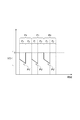
 図1は、一つの例示的実施形態に係るプラズマ処理装置を概略的に示す図である。図1に示すプラズマ処理装置1は、容量結合型のプラズマ処理装置である。プラズマ処理装置1は、チャンバ10を備えている。チャンバ10は、その中に内部空間10sを提供している。内部空間10sの中心軸線は、鉛直方向に延びる軸線AXである。 FIG. 1 is a diagram schematically showing a plasma processing apparatus according to an exemplary embodiment. The plasma processing apparatus 1 shown in FIG. 1 is a capacitively coupled plasma processing apparatus. The plasma processing apparatus 1 includes a chamber 10. The chamber 10 provides an internal space 10s therein. The central axis of the internal space 10s is an axis AX extending in the vertical direction.
 一実施形態において、チャンバ10は、チャンバ本体12を含んでいる。チャンバ本体12は、略円筒形状を有している。内部空間10sは、チャンバ本体12の中に提供されている。チャンバ本体12は、例えばアルミニウムから構成されている。チャンバ本体12は電気的に接地されている。チャンバ本体12の内壁面、即ち内部空間10sを画成する壁面には、耐プラズマ性を有する膜が形成されている。この膜は、陽極酸化処理によって形成された膜又は酸化イットリウムから形成された膜といったセラミック製の膜であり得る。 In one embodiment, the chamber 10 includes a chamber body 12. The chamber body 12 has a substantially cylindrical shape. The internal space 10s is provided in the chamber body 12. The chamber body 12 is made of, for example, aluminum. The chamber body 12 is electrically grounded. A film having plasma resistance is formed on the inner wall surface of the chamber body 12, that is, the wall surface defining the internal space 10s. This film may be a ceramic film such as a film formed by anodization or a film formed from yttrium oxide.
 チャンバ本体12の側壁には通路12pが形成されている。基板Wは、内部空間10sとチャンバ10の外部との間で搬送されるときに、通路12pを通過する。この通路12pの開閉のために、ゲートバルブ12gがチャンバ本体12の側壁に沿って設けられている。 A passage 12p is formed on the side wall of the chamber body 12. The substrate W passes through the passage 12p when being transferred between the internal space 10s and the outside of the chamber 10. A gate valve 12g is provided along the side wall of the chamber body 12 for opening and closing the passage 12p.
 プラズマ処理装置1は、基板支持器16を更に備える。基板支持器16は、チャンバ10の中で、その上に載置された基板Wを支持するように構成されている。基板Wは、略円盤形状を有する。基板支持器16は、支持部17によって支持されている。支持部17は、チャンバ本体12の底部から上方に延在している。支持部17は、略円筒形状を有している。支持部17は、石英といった絶縁材料から形成されている。 The plasma processing apparatus 1 further includes a substrate supporter 16. The substrate supporter 16 is configured to support the substrate W placed thereon in the chamber 10. The substrate W has a substantially disc shape. The substrate supporter 16 is supported by the support portion 17. The support portion 17 extends upward from the bottom portion of the chamber body 12. The support portion 17 has a substantially cylindrical shape. The support 17 is made of an insulating material such as quartz.
 基板支持器16は、下部電極18及び静電チャック20を有する。下部電極18及び静電チャック20は、チャンバ10の中に設けられている。下部電極18は、アルミニウムといった導電性材料から形成されており、略円盤形状を有している。 The substrate support 16 has a lower electrode 18 and an electrostatic chuck 20. The lower electrode 18 and the electrostatic chuck 20 are provided inside the chamber 10. The lower electrode 18 is made of a conductive material such as aluminum and has a substantially disc shape.
 下部電極18内には、流路18fが形成されている。流路18fは、熱交換媒体用の流路である。熱交換媒体としては、液状の冷媒、或いは、その気化によって下部電極18を冷却する冷媒(例えば、フロン)が用いられる。流路18fには、熱交換媒体の供給装置(例えば、チラーユニット)が接続されている。この供給装置は、チャンバ10の外部に設けられている。流路18fには、供給装置から配管23aを介して熱交換媒体が供給される。流路18fに供給された熱交換媒体は、配管23bを介して供給装置に戻される。 A flow path 18f is formed in the lower electrode 18. The flow path 18f is a flow path for a heat exchange medium. As the heat exchange medium, a liquid coolant or a coolant (for example, CFC) that cools the lower electrode 18 by vaporization thereof is used. A supply device (for example, a chiller unit) for the heat exchange medium is connected to the flow path 18f. This supply device is provided outside the chamber 10. The heat exchange medium is supplied to the flow path 18f from the supply device through the pipe 23a. The heat exchange medium supplied to the flow path 18f is returned to the supply device via the pipe 23b.
 静電チャック20は、下部電極18上に設けられている。基板Wは、内部空間10sの中で処理されるときに、静電チャック20上に載置され、静電チャック20によって保持される。 The electrostatic chuck 20 is provided on the lower electrode 18. The substrate W is placed on and held by the electrostatic chuck 20 when being processed in the internal space 10 s.
 静電チャック20は、本体及び電極を有している。静電チャック20の本体は、酸化アルミニウム又は窒化アルミニウムといった誘電体から形成されている。静電チャック20の本体は、略円盤形状を有している。静電チャック20の中心軸線は、軸線AXに略一致している。静電チャック20の電極は、本体内に設けられている。静電チャック20の電極は、膜形状を有している。静電チャック20の電極には、直流電源がスイッチを介して電気的に接続されている。直流電源からの電圧が静電チャック20の電極に印加されると、静電チャック20と基板Wとの間で静電引力が発生する。発生した静電引力により、基板Wは静電チャック20に引き付けられ、静電チャック20によって保持される。 The electrostatic chuck 20 has a main body and electrodes. The body of the electrostatic chuck 20 is formed of a dielectric material such as aluminum oxide or aluminum nitride. The main body of the electrostatic chuck 20 has a substantially disc shape. The central axis of the electrostatic chuck 20 substantially coincides with the axis AX. The electrodes of the electrostatic chuck 20 are provided inside the main body. The electrode of the electrostatic chuck 20 has a film shape. A DC power supply is electrically connected to the electrodes of the electrostatic chuck 20 via a switch. When the voltage from the DC power supply is applied to the electrodes of the electrostatic chuck 20, electrostatic attraction is generated between the electrostatic chuck 20 and the substrate W. The substrate W is attracted to and held by the electrostatic chuck 20 by the generated electrostatic attraction.
 静電チャック20は、基板載置領域を含んでいる。基板載置領域は、略円盤形状を有する領域である。基板載置領域の中心軸線は、軸線AXに略一致している。基板Wは、チャンバ10内で処理されるときには、基板載置領域の上面の上に載置される。 The electrostatic chuck 20 includes a substrate mounting area. The substrate mounting area is an area having a substantially disc shape. The central axis of the substrate mounting area substantially coincides with the axis AX. The substrate W is mounted on the upper surface of the substrate mounting area when being processed in the chamber 10.
 一実施形態において、静電チャック20は、エッジリング載置領域を更に含んでいてもよい。エッジリング載置領域は、静電チャック20の中心軸線の周りで基板載置領域を囲むように周方向に延在している。エッジリング載置領域の上面の上にはエッジリングERが搭載される。エッジリングERは、環形状を有している。エッジリングERは、軸線AXにその中心軸線が一致するように、エッジリング載置領域上に載置される。基板Wは、エッジリングERによって囲まれた領域内に配置される。即ち、エッジリングERは、基板Wのエッジを囲むように配置される。エッジリングERは、導電性を有し得る。エッジリングERは、例えばシリコン又は炭化ケイ素から形成されている。エッジリングERは、石英といった誘電体から形成されていてもよい。 In one embodiment, the electrostatic chuck 20 may further include an edge ring mounting area. The edge ring mounting area extends in the circumferential direction around the central axis of the electrostatic chuck 20 so as to surround the substrate mounting area. The edge ring ER is mounted on the upper surface of the edge ring mounting area. The edge ring ER has a ring shape. The edge ring ER is mounted on the edge ring mounting area so that its central axis coincides with the axis AX. The substrate W is arranged in a region surrounded by the edge ring ER. That is, the edge ring ER is arranged so as to surround the edge of the substrate W. The edge ring ER can have conductivity. The edge ring ER is made of, for example, silicon or silicon carbide. The edge ring ER may be formed of a dielectric material such as quartz.
 プラズマ処理装置1は、ガス供給ライン25を更に備え得る。ガス供給ライン25は、ガス供給機構からの伝熱ガス、例えばHeガスを、静電チャック20の上面と基板Wの裏面(下面)との間の間隙に供給する。 The plasma processing apparatus 1 may further include a gas supply line 25. The gas supply line 25 supplies the heat transfer gas, for example, He gas, from the gas supply mechanism to the gap between the upper surface of the electrostatic chuck 20 and the back surface (lower surface) of the substrate W.
 プラズマ処理装置1は、絶縁領域27を更に備え得る。絶縁領域27は、支持部17上に配置されている。絶縁領域27は、軸線AXに対して径方向において下部電極18の外側に配置されている。絶縁領域27は、下部電極18の外周面に沿って周方向に延在している。絶縁領域27は、石英といった絶縁体から形成されている。エッジリングERは、絶縁領域27及びエッジリング載置領域上に載置される。 The plasma processing apparatus 1 may further include an insulating region 27. The insulating region 27 is arranged on the support portion 17. The insulating region 27 is arranged outside the lower electrode 18 in the radial direction with respect to the axis AX. The insulating region 27 extends in the circumferential direction along the outer peripheral surface of the lower electrode 18. The insulating region 27 is made of an insulating material such as quartz. The edge ring ER is mounted on the insulating area 27 and the edge ring mounting area.
 プラズマ処理装置1は、上部電極30を更に備えている。上部電極30は、基板支持器16の上方に設けられている。上部電極30は、部材32と共にチャンバ本体12の上部開口を閉じている。部材32は、絶縁性を有している。上部電極30は、この部材32を介してチャンバ本体12の上部に支持されている。 The plasma processing apparatus 1 further includes an upper electrode 30. The upper electrode 30 is provided above the substrate support 16. The upper electrode 30 closes the upper opening of the chamber body 12 together with the member 32. The member 32 has an insulating property. The upper electrode 30 is supported on the upper portion of the chamber body 12 via the member 32.
 上部電極30は、天板34及び支持体36を含んでいる。天板34の下面は、内部空間10sを画成している。天板34には、複数のガス吐出孔34aが形成されている。複数のガス吐出孔34aの各々は、天板34を板厚方向(鉛直方向)に貫通している。この天板34は、限定されるものではないが、例えばシリコンから形成されている。或いは、天板34は、アルミニウム製の部材の表面に耐プラズマ性の膜を設けた構造を有し得る。この膜は、陽極酸化処理によって形成された膜又は酸化イットリウムから形成された膜といったセラミック製の膜であり得る。 The upper electrode 30 includes a top plate 34 and a support body 36. The lower surface of the top plate 34 defines the internal space 10s. The top plate 34 is formed with a plurality of gas discharge holes 34a. Each of the plurality of gas discharge holes 34a penetrates the top plate 34 in the plate thickness direction (vertical direction). The top plate 34 is made of, for example, but not limited to, silicon. Alternatively, the top plate 34 may have a structure in which a plasma resistant film is provided on the surface of an aluminum member. This film may be a ceramic film such as a film formed by anodization or a film formed from yttrium oxide.
 支持体36は、天板34を着脱自在に支持している。支持体36は、例えばアルミニウムといった導電性材料から形成されている。支持体36の内部には、ガス拡散室36aが設けられている。ガス拡散室36aからは、複数のガス孔36bが下方に延びている。複数のガス孔36bは、複数のガス吐出孔34aにそれぞれ連通している。支持体36には、ガス導入ポート36cが形成されている。ガス導入ポート36cは、ガス拡散室36aに接続している。ガス導入ポート36cには、ガス供給管38が接続されている。 The support body 36 detachably supports the top plate 34. The support 36 is made of a conductive material such as aluminum. A gas diffusion space 36 a is provided inside the support 36. A plurality of gas holes 36b extend downward from the gas diffusion chamber 36a. The plurality of gas holes 36b communicate with the plurality of gas discharge holes 34a, respectively. A gas introduction port 36c is formed in the support 36. The gas introduction port 36c is connected to the gas diffusion chamber 36a. A gas supply pipe 38 is connected to the gas introduction port 36c.
 ガス供給管38には、ガスソース群40が、バルブ群41、流量制御器群42、及びバルブ群43を介して接続されている。ガスソース群40、バルブ群41、流量制御器群42、及びバルブ群43は、ガス供給部を構成している。ガスソース群40は、複数のガスソースを含んでいる。バルブ群41及びバルブ群43の各々は、複数のバルブ(例えば開閉バルブ)を含んでいる。流量制御器群42は、複数の流量制御器を含んでいる。流量制御器群42の複数の流量制御器の各々は、マスフローコントローラ又は圧力制御式の流量制御器である。ガスソース群40の複数のガスソースの各々は、バルブ群41の対応のバルブ、流量制御器群42の対応の流量制御器、及びバルブ群43の対応のバルブを介して、ガス供給管38に接続されている。プラズマ処理装置1は、ガスソース群40の複数のガスソースのうち選択された一以上のガスソースからのガスを、個別に調整された流量で、内部空間10sに供給することが可能である。 A gas source group 40 is connected to the gas supply pipe 38 via a valve group 41, a flow rate controller group 42, and a valve group 43. The gas source group 40, the valve group 41, the flow rate controller group 42, and the valve group 43 form a gas supply unit. The gas source group 40 includes a plurality of gas sources. Each of the valve group 41 and the valve group 43 includes a plurality of valves (for example, opening/closing valves). The flow rate controller group 42 includes a plurality of flow rate controllers. Each of the plurality of flow rate controllers in the flow rate controller group 42 is a mass flow controller or a pressure control type flow rate controller. Each of the plurality of gas sources of the gas source group 40 is connected to the gas supply pipe 38 via the corresponding valve of the valve group 41, the corresponding flow rate controller of the flow rate controller group 42, and the corresponding valve of the valve group 43. It is connected. The plasma processing apparatus 1 can supply gas from one or more gas sources selected from the plurality of gas sources of the gas source group 40 to the internal space 10s at individually adjusted flow rates.
 基板支持器16又は支持部17とチャンバ本体12の側壁との間には、バッフルプレート48が設けられている。バッフルプレート48は、例えば、アルミニウム製の部材に酸化イットリウム等のセラミックを被覆することにより構成され得る。このバッフルプレート48には、多数の貫通孔が形成されている。バッフルプレート48の下方においては、排気管52がチャンバ本体12の底部に接続されている。この排気管52には、排気装置50が接続されている。排気装置50は、自動圧力制御弁といった圧力制御器、及び、ターボ分子ポンプなどの真空ポンプを有しており、内部空間10sの圧力を減圧することができる。 A baffle plate 48 is provided between the substrate support 16 or the support 17 and the side wall of the chamber body 12. The baffle plate 48 can be formed by, for example, coating an aluminum member with a ceramic such as yttrium oxide. A large number of through holes are formed in the baffle plate 48. Below the baffle plate 48, an exhaust pipe 52 is connected to the bottom of the chamber body 12. An exhaust device 50 is connected to the exhaust pipe 52. The exhaust device 50 has a pressure controller such as an automatic pressure control valve and a vacuum pump such as a turbo molecular pump, and can reduce the pressure in the internal space 10s.
 プラズマ処理装置1は、高周波電源61を更に備えている。高周波電源61は、高周波電力RFを発生する電源である。高周波電力RFは、チャンバ10内のガスからプラズマを生成するために用いられる。高周波電力RFは、第1の周波数を有する。第1の周波数は、27~100MHzの範囲内の周波数、例えば40MHz又は60MHzの周波数である。高周波電源61は、高周波電力RFを下部電極18に供給するために、整合回路63を介して下部電極18に接続されている。整合回路63は、高周波電源61の出力インピーダンスと負荷側(下部電極18側)のインピーダンスを整合させるよう構成されている。なお、高周波電源61は、下部電極18に電気的に接続されていなくてもよく、整合回路63を介して上部電極30に接続されていてもよい。 The plasma processing apparatus 1 further includes a high frequency power supply 61. The high frequency power supply 61 is a power supply that generates high frequency power RF. The radio frequency power RF is used to generate plasma from the gas in the chamber 10. The radio frequency power RF has a first frequency. The first frequency is a frequency within the range of 27-100 MHz, for example a frequency of 40 MHz or 60 MHz. The high frequency power supply 61 is connected to the lower electrode 18 via a matching circuit 63 in order to supply the high frequency power RF to the lower electrode 18. The matching circuit 63 is configured to match the output impedance of the high frequency power supply 61 and the impedance of the load side (lower electrode 18 side). The high frequency power supply 61 may not be electrically connected to the lower electrode 18 and may be connected to the upper electrode 30 via the matching circuit 63.
 プラズマ処理装置1は、バイアス電源62を更に備えている。バイアス電源62は、下部電極18に電気的に接続されている。一実施形態において、バイアス電源62は、ローパスフィルタ64を介して下部電極18に電気的に接続されている。バイアス電源62は、第2の周波数で規定される周期P、即ちパルス周期で周期的にパルス状の負極性の直流電圧PVを下部電極18に印加するように構成されている。第2の周波数は、第1の周波数よりも低い。第2の周波数は、例えば、50kHz以上、27MHz以下である。 The plasma processing apparatus 1 further includes a bias power supply 62. The bias power source 62 is electrically connected to the lower electrode 18. In one embodiment, the bias power supply 62 is electrically connected to the lower electrode 18 via the low pass filter 64. The bias power supply 62 is configured to apply a pulsed negative DC voltage PV to the lower electrode 18 periodically with a period P P defined by the second frequency, that is, a pulse period. The second frequency is lower than the first frequency. The second frequency is, for example, 50 kHz or more and 27 MHz or less.
 プラズマ処理装置1においてプラズマ処理が行われる場合には、内部空間10sにガスが供給される。そして、高周波電力RFが供給されることにより、内部空間10sの中でガスが励起される。その結果、内部空間10sの中でプラズマが生成される。基板支持器16によって支持された基板Wは、プラズマからのイオン及びラジカルといった化学種により処理される。例えば、基板は、プラズマからの化学種によりエッチングされる。プラズマ処理装置1では、パルス状の負極性の直流電圧PVが下部電極18に印加されることにより、プラズマからのイオンが基板Wに向けて加速される。 When plasma processing is performed in the plasma processing apparatus 1, gas is supplied to the internal space 10s. Then, by supplying the high frequency power RF, the gas is excited in the internal space 10s. As a result, plasma is generated in the internal space 10s. The substrate W supported by the substrate support 16 is treated with chemical species such as ions and radicals from plasma. For example, the substrate is etched with species from the plasma. In the plasma processing apparatus 1, the pulsed negative DC voltage PV is applied to the lower electrode 18, whereby ions from the plasma are accelerated toward the substrate W.
 プラズマ処理装置1は、制御部MCを更に備える。制御部MCは、プロセッサ、記憶装置、入力装置、表示装置等を備えるコンピュータであり、プラズマ処理装置1の各部を制御する。制御部MCは、記憶装置に記憶されている制御プログラムを実行し、当該記憶装置に記憶されているレシピデータに基づいてプラズマ処理装置1の各部を制御する。制御部MCによる制御により、レシピデータによって指定されたプロセスがプラズマ処理装置1において実行される。後述するプラズマ処理方法は、制御部MCによるプラズマ処理装置1の各部の制御により、プラズマ処理装置1において実行され得る。 The plasma processing apparatus 1 further includes a control unit MC. The control unit MC is a computer including a processor, a storage device, an input device, a display device, and the like, and controls each unit of the plasma processing apparatus 1. The control unit MC executes the control program stored in the storage device, and controls each unit of the plasma processing apparatus 1 based on the recipe data stored in the storage device. Under the control of the control unit MC, the process specified by the recipe data is executed in the plasma processing apparatus 1. The plasma processing method described below can be executed in the plasma processing apparatus 1 by the control of each unit of the plasma processing apparatus 1 by the control unit MC.
 制御部MCは、周期P内の第1の部分期間P内の少なくとも一部の期間において高周波電力RFを供給するように高周波電源61を制御する。プラズマ処理装置1では、高周波電力RFは、下部電極18に供給される。或いは、高周波電力RFは、上部電極30に供給されてもよい。制御部MCは、周期P内の第2の部分期間Pにおける高周波電力RFのパワーレベルを、第1の部分期間Pにおける高周波電力RFのパワーレベルから減少されたパワーレベルに設定する。即ち、制御部MCは、第1の部分期間Pにおいて高周波電力RFの一つ以上のパルスPRFを供給するように高周波電源61を制御する。 Controller MC controls the high frequency power source 61 to supply a high frequency power RF in the first sub-period at least part of the period P 1 of the period P P. In the plasma processing apparatus 1, the high frequency power RF is supplied to the lower electrode 18. Alternatively, the high frequency power RF may be supplied to the upper electrode 30. The control unit MC sets the power level of the high frequency power RF in the second partial period P 2 in the cycle P P to a power level reduced from the power level of the high frequency power RF in the first partial period P 1 . That is, the control unit MC controls the high frequency power supply 61 so as to supply one or more pulses PRF of the high frequency power RF in the first partial period P 1 .
 第2の部分期間Pにおける高周波電力RFのパワーレベルは、0[W]であってもよい。即ち、制御部MCは、第2の部分期間Pにおいては、高周波電力RFの供給を停止するように、高周波電源61を制御してもよい。或いは、第2の部分期間Pにおける高周波電力RFのパワーレベルは、0[W]よりも大きくてもよい。 The power level of the high frequency power RF in the second partial period P 2 may be 0 [W]. That is, the control unit MC may control the high frequency power supply 61 so as to stop the supply of the high frequency power RF in the second partial period P 2 . Alternatively, the power level of the high frequency power RF in the second partial period P 2 may be larger than 0 [W].
 制御部MCは、同期パルス、遅延時間長、及び供給時間長が制御部MCを高周波電源61に与えるように構成されている。同期パルスは、パルス状の負極性の直流電圧PVに同期されている。遅延時間長は、同期パルスによって特定される周期Pの開始時点からの遅延時間長である。供給時間長は、高周波電力RFの供給時間の長さである。高周波電源61は、周期Pの開始時点に対して遅延時間長だけ遅れた時点から供給時間長の間、高周波電力RFの一つ以上のパルスPRFを供給する。その結果、第1の部分期間Pにおいて、高周波電力RFが下部電極18に供給される。なお、遅延時間長は、ゼロであってもよい。 The control unit MC is configured such that the synchronization pulse, the delay time length, and the supply time length give the control unit MC to the high frequency power supply 61. The synchronization pulse is synchronized with the pulsed negative DC voltage PV. The delay time length is the delay time length from the start point of the period P P specified by the sync pulse. The supply time length is the length of the supply time of the high frequency power RF. The high frequency power supply 61 supplies one or more pulses PRF of the high frequency power RF during the supply time length from the time delayed by the delay time length with respect to the start time of the period P P. As a result, the high frequency power RF is supplied to the lower electrode 18 in the first partial period P 1 . The delay time length may be zero.
 一実施形態において、プラズマ処理装置1は、電圧センサ78を更に備えていてもよい。電圧センサ78は、基板Wの電位を直接的に又は間接的に測定するように構成されている。図1に示す例では、電圧センサ78は、下部電極18の電位を測定するように構成されている。具体的には、電圧センサ78は、下部電極18とバイアス電源62との間で接続されている給電路の電位を測定する。 In one embodiment, the plasma processing apparatus 1 may further include a voltage sensor 78. The voltage sensor 78 is configured to directly or indirectly measure the potential of the substrate W. In the example shown in FIG. 1, the voltage sensor 78 is configured to measure the potential of the lower electrode 18. Specifically, the voltage sensor 78 measures the potential of the power feeding path connected between the lower electrode 18 and the bias power source 62.
 制御部MCは、電圧センサ78によって測定された基板Wの電位が周期Pにおける基板Wの電位の平均値VAVEよりも高いか又は低い期間を第1の部分期間Pとして決定してもよい。制御部MCは、電圧センサ78によって測定された基板Wの電位が平均値VAVEよりも低いか又は高い期間を第2の部分期間Pとして決定してもよい。基板Wの電位の平均値VAVEは、予め定められた値であってもよい。制御部MCは、決定した第1の部分期間Pにおいて上述したように高周波電力RFを供給するように高周波電源61を制御し得る。また、制御部MCは、決定した第2の部分期間Pにおいて上述したように高周波電力RFのパワーレベルを設定するように高周波電源61を制御し得る。 The control unit MC determines the period in which the potential of the substrate W measured by the voltage sensor 78 is higher or lower than the average value V AVE of the potential of the substrate W in the period P P as the first partial period P 1. Good. The control unit MC may determine a period in which the potential of the substrate W measured by the voltage sensor 78 is lower or higher than the average value V AVE as the second partial period P 2 . The average value V AVE of the potential of the substrate W may be a predetermined value. The control unit MC can control the high frequency power supply 61 to supply the high frequency power RF as described above in the determined first partial period P 1 . In addition, the control unit MC can control the high frequency power supply 61 so as to set the power level of the high frequency power RF as described above in the determined second partial period P 2 .
 プラズマ処理装置1では、パルス状の負極性の直流電圧PVが周期Pで周期的に下部電極18に供給されるので、基板Wの電位が周期P内において変動する。周期P内の第1の部分期間Pでは、周期P内の第2の部分期間Pにおける高周波電力RFのパワーレベルよりも高いパワーレベルを有する高周波電力RFが供給される。したがって、基板Wに供給されるイオンのエネルギーは、周期P内での第1の部分期間P及び第2の部分期間Pの各々の時間範囲の設定に依存する。故に、プラズマ処理装置1によれば、プラズマから基板Wに供給されるイオンのエネルギーを制御することが可能となる。 In the plasma processing apparatus 1, since the pulsed negative DC voltage PV is periodically supplied to the lower electrode 18 at a period P P, the potential of the substrate W varies in the cycle P P. In the first part period P 1 in the period P P, the high-frequency power RF is supplied with a higher power level than the high frequency power RF power level in the second partial periods P 2 in the cycle P P. Thus, ions of energy supplied to the substrate W depends on the setting of the first partial period P 1 and the second time range for each partial period P 2 in the cycle P P. Therefore, according to the plasma processing apparatus 1, it is possible to control the energy of the ions supplied from the plasma to the substrate W.
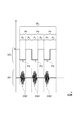
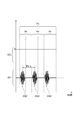
 図2は、一例に係る高周波電力及びパルス状の負極性の直流電圧のタイミングチャートである。図2において、「VO」は、バイアス電源62の出力電圧を示しており、「RF」は、高周波電力RFのパワーレベルを示している。図2に示す例では、第1の部分期間Pは、パルス状の負極性の直流電圧PVが下部電極18に印加される期間である。図2に示す例では、第2の部分期間Pは、パルス状の負極性の直流電圧PVが下部電極18に印加されない期間である。図2に示す例では、第1の部分期間Pにおいて高周波電力RFの一つのパルスPRFが供給されている。この例によれば、比較的高いエネルギーを有するイオンが基板Wに供給され得る。 FIG. 2 is a timing chart of the high frequency power and the pulsed negative DC voltage according to an example. In FIG. 2, “VO” indicates the output voltage of the bias power supply 62, and “RF” indicates the power level of the high frequency power RF. In the example shown in FIG. 2, the first partial period P 1 is a period in which the pulsed negative DC voltage PV is applied to the lower electrode 18. In the example shown in FIG. 2, the second partial period P 2 is a period in which the pulsed negative DC voltage PV is not applied to the lower electrode 18. In the example shown in FIG. 2, one pulse PRF of the high frequency power RF is supplied in the first partial period P 1 . According to this example, ions having a relatively high energy can be supplied to the substrate W.
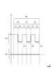
 図3は、別の例に係る高周波電力及びパルス状の負極性の直流電圧のタイミングチャートである。図3において、「VO」は、バイアス電源62の出力電圧を示しており、「RF」は、高周波電力RFのパワーレベルを示している。図3に示す例では、第1の部分期間Pは、パルス状の負極性の直流電圧PVが下部電極18に印加されない期間である。図3に示す例では、第2の部分期間Pは、パルス状の負極性の直流電圧PVが下部電極18に印加される期間である。図3に示す例では、第1の部分期間Pにおいて高周波電力RFの一つのパルスPRFが供給されている。この例によれば、比較的低いエネルギーを有するイオンが基板Wに供給され得る。 FIG. 3 is a timing chart of high-frequency power and a pulsed negative DC voltage according to another example. In FIG. 3, “VO” indicates the output voltage of the bias power supply 62, and “RF” indicates the power level of the high frequency power RF. In the example shown in FIG. 3, the first partial period P 1 is a period in which the pulsed negative DC voltage PV is not applied to the lower electrode 18. In the example shown in FIG. 3, the second partial period P 2 is a period in which the pulsed negative DC voltage PV is applied to the lower electrode 18. In the example shown in FIG. 3, one pulse PRF of the high frequency power RF is supplied in the first partial period P 1 . According to this example, ions having a relatively low energy can be supplied to the substrate W.
 図4は、更に別の例に係るパルス状の負極性の直流電圧のタイミングチャートである。図4において、「VO」は、バイアス電源62の出力電圧を示している。図4に示すように、パルス状の負極性の直流電圧PVの電圧レベルは、それが下部電極18に印加されている期間内において、変化してもよい。図4に示す例では、パルス状の負極性の直流電圧PVの電圧レベルは、それが下部電極18に印加されている期間内において、低下している。即ち、図4に示す例では、パルス状の負極性の直流電圧PVの電圧レベルの絶対値は、それが下部電極18に印加されている期間内において、増加している。なお、パルス状の負極性の直流電圧PVは、第1の部分期間Pにおいて下部電極18に印加されてもよく、或いは、第2の部分期間Pにおいて下部電極18に印加されてもよい。 FIG. 4 is a timing chart of a pulsed negative DC voltage according to still another example. In FIG. 4, “VO” indicates the output voltage of the bias power supply 62. As shown in FIG. 4, the voltage level of the pulsed DC voltage PV having the negative polarity may change within the period in which it is applied to the lower electrode 18. In the example shown in FIG. 4, the voltage level of the pulsed negative DC voltage PV is lowered during the period in which it is applied to the lower electrode 18. That is, in the example shown in FIG. 4, the absolute value of the voltage level of the pulsed negative DC voltage PV increases during the period in which it is applied to the lower electrode 18. The pulsed negative DC voltage PV may be applied to the lower electrode 18 in the first partial period P 1 or may be applied to the lower electrode 18 in the second partial period P 2 . ..
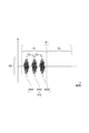
 図5は、更に別の例に係る高周波電力のタイミングチャートである。図5において、「RF」は、高周波電力RFのパワーレベルを示している。図5に示すように、制御部MCは、第1の部分期間Pにおいて、高周波電力RFの複数のパルスPRFを順に供給するように高周波電源61を制御してもよい。即ち、制御部MCは、第1の部分期間Pにおいて、複数のパルスPRFを含むパルス群PGを供給するように高周波電源61を制御してもよい。第1の部分期間Pにおいて、高周波電力RFのパルスPRFは、周期的に供給されてもよい。第1の部分期間Pにおいて高周波電力RFのパルスPRFが供給される周期PRFGを規定する周波数は、第2の周波数の2倍以上、且つ、第1の周波数の0.5倍以下であり得る。 FIG. 5 is a timing chart of high frequency power according to still another example. In FIG. 5, “RF” indicates the power level of the high frequency power RF. As shown in FIG. 5, the control unit MC may control the high frequency power supply 61 so as to sequentially supply a plurality of pulses PRF of the high frequency power RF in the first partial period P 1 . That is, the control unit MC may control the high frequency power supply 61 so as to supply the pulse group PG including the plurality of pulses PRF in the first partial period P 1 . In the first partial period P 1 , the pulse PRF of the high frequency power RF may be periodically supplied. The frequency that defines the period P RFG in which the pulse PRF of the high-frequency power RF is supplied in the first partial period P 1 is twice or more the second frequency and 0.5 times or less the first frequency. obtain.
 図6は、更に別の例に係る高周波電力及びパルス状の負極性の直流電圧のタイミングチャートである。図6において、「VO」は、バイアス電源62の出力電圧を示しており、「RF」は、高周波電力RFのパワーレベルを示している。プラズマ処理装置1は、図2又は図3に示す例のように、期間Pにおいて、パルス状の負極性の直流電圧PVを周期Pで周期的に下部電極18に印加し、且つ、周期P内において高周波電力RFの一つ以上のパルスPRFを供給する。図6に示すように、制御部MCは、別の期間Pにおいて、高周波電力RFの供給を停止するように高周波電源61を制御してもよい。期間Pにおいて、制御部MCは、高周波電力RFの供給が停止されている状態で、周期Pで周期的に下部電極18にパルス状の負極性の直流電圧PVを印加するようにバイアス電源62を制御してもよい。期間Pは、周期Pの時間長よりも長い時間長を有する期間である。期間Pは、チャンバ10内でプラズマが存在している期間であり得る。期間Pは、例えば、期間Pに続く期間であり得る。 FIG. 6 is a timing chart of the high frequency power and the pulsed negative DC voltage according to still another example. In FIG. 6, “VO” indicates the output voltage of the bias power supply 62, and “RF” indicates the power level of the high frequency power RF. As in the example shown in FIG. 2 or FIG. 3, the plasma processing apparatus 1 periodically applies the pulsed negative DC voltage PV to the lower electrode 18 at the period P P in the period P A , and Providing one or more pulses PRF of RF power RF in P P. As shown in FIG. 6, the control unit MC may control the high frequency power supply 61 so as to stop the supply of the high frequency power RF in another period P B. In the period P B , the control unit MC, in a state where the supply of the high frequency power RF is stopped, periodically applies the pulsed negative DC voltage PV to the lower electrode 18 at the period P P. 62 may be controlled. The period P B is a period having a time length longer than the time length of the period P P. The period P B may be a period during which plasma is present in the chamber 10. The period P B can be, for example, a period following the period P A.
 図7は、更に別の例に係る高周波電力及びパルス状の負極性の直流電圧のタイミングチャートである。図7において、「VO」は、バイアス電源62の出力電圧を示しており、「RF」は、高周波電力RFのパワーレベルを示している。図7に示すように、制御部MCは、別の期間Pにおいて、下部電極18に対するパルス状の負極性の直流電圧PVの印加を停止するようにバイアス電源62を制御してもよい。期間Pにおいて、制御部MCは、下部電極18に対するパルス状の負極性の直流電圧PVの印加が停止されている状態で、高周波電力RFを供給するように高周波電源61を制御してもよい。制御部MCは、期間Pにおいて、高周波電力RFのパルスPRF又はパルス群PGを周期的に供給するように高周波電源61を制御し得る。期間Pにおける高周波電力RFのパルスPRF又はパルス群PGの供給の周期PRFCは、期間Pにおける高周波電力RFのパルスPRF又はパルス群PGの供給の周期、即ち周期Pと同じ周期であり得る。なお、期間Pにおいても、パルス群PGを形成する高周波電力RFのパルスPRFの供給の周期PRFGを規定する周波数は、第2の周波数の2倍以上、且つ、第1の周波数の0.5倍以下であり得る。 FIG. 7 is a timing chart of the high frequency power and the pulsed negative DC voltage according to still another example. In FIG. 7, “VO” indicates the output voltage of the bias power supply 62, and “RF” indicates the power level of the high frequency power RF. 7, the control unit MC is, in another period P C, may control the bias power source 62 so as to stop the application of pulsed negative DC voltage PV to the lower electrode 18. In the period P C, the control unit MC in a state where the application of the pulsed negative DC voltage PV to the lower electrode 18 is stopped, it may control the high frequency power source 61 to supply a high frequency power RF .. Control unit MC in the period P C, may control the high frequency power source 61 to supply a pulse PRF or pulse group PG of the RF power RF periodically. The period P RFC of supplying the pulse PRF of the high frequency power RF or the pulse group PG in the period P C is the same period as the period of supply of the pulse PRF of the high frequency power RF or the pulse group PG in the period P A , that is, the period P P. obtain. Also in the period P C , the frequency defining the supply period P RFG of the pulse PRF of the high-frequency power RF forming the pulse group PG is at least twice the second frequency and 0. It can be 5 times or less.
 図8の(a)及び図8の(b)の各々は、更に別の例に係るパルス状の負極性の直流電圧のタイミングチャートである。図8の(a)に示す例におけるバイアス電源62の出力電圧VOは、その極性が第2の部分期間P内且つ第1の部分期間Pの直前に正極性に変更されている点で、図2に示す例におけるバイアス電源62の出力電圧VOと異なっている。即ち、図8の(a)に示す例では、正極性の直流電圧が、第2の部分期間P内且つ第1の部分期間Pの直前に、バイアス電源62から下部電極18に印加されている。なお、パルス状の負極性の直流電圧PVが第1の部分期間P内に下部電極18に印加される場合には、第2の部分期間Pの少なくとも一部において、正極性の直流電圧がバイアス電源62から下部電極18に印加されてもよい。 FIGS. 8A and 8B are timing charts of pulsed negative DC voltage according to still another example. The output voltage VO of the bias power supply 62 in the example shown in FIG. 8A is changed in its polarity to the positive polarity within the second partial period P 2 and immediately before the first partial period P 1. 2, which is different from the output voltage VO of the bias power supply 62 in the example shown in FIG. That is, in the example shown in FIG. 8A, the positive DC voltage is applied from the bias power source 62 to the lower electrode 18 within the second partial period P 2 and immediately before the first partial period P 1. ing. When the pulsed negative DC voltage PV is applied to the lower electrode 18 within the first partial period P 1 , the positive DC voltage is applied at least in a part of the second partial period P 2. May be applied to the lower electrode 18 from the bias power supply 62.
 図8の(b)に示す例におけるバイアス電源62の出力電圧VOは、その極性が第1の部分期間P内且つ第2の部分期間Pの直前に正極性に変更されている点で、図3に示す例におけるバイアス電源62の出力電圧VOと異なっている。即ち、図8の(b)に示す例では、正極性の直流電圧が、第1の部分期間P内且つ第2の部分期間Pの直前に、バイアス電源62から下部電極18に印加されている。なお、パルス状の負極性の直流電圧PVが第2の部分期間P内に下部電極18に印加される場合には、第1の部分期間Pの少なくとも一部において、正極性の直流電圧がバイアス電源62から下部電極18に印加されてもよい。 The output voltage VO of the bias power supply 62 in the example shown in FIG. 8B is changed in its polarity to the positive polarity within the first partial period P 1 and immediately before the second partial period P 2. , The output voltage VO of the bias power supply 62 in the example shown in FIG. That is, in the example shown in FIG. 8B, a positive DC voltage is applied from the bias power supply 62 to the lower electrode 18 within the first partial period P 1 and immediately before the second partial period P 2. ing. If the pulsed negative DC voltage PV is applied to the lower electrode 18 within the second partial period P 2 , the positive DC voltage PV is applied at least in a part of the first partial period P 1. May be applied to the lower electrode 18 from the bias power supply 62.
 以下、図9を参照する。図9は、一つの例示的実施形態に係るプラズマ処理方法を示す流れ図である。図9に示すプラズマ処理方法(以下、「方法MT」という)は、上述したプラズマ処理装置1を用いて実行され得る。 Refer to FIG. 9 below. FIG. 9 is a flow chart illustrating a plasma processing method according to an exemplary embodiment. The plasma processing method shown in FIG. 9 (hereinafter referred to as “method MT”) can be executed using the plasma processing apparatus 1 described above.
 方法MTは、静電チャック20上に基板Wが載置されている状態で実行される。方法MTは、基板Wにプラズマ処理を行うために実行される。方法MTでは、ガスがガス供給部からチャンバ10内に供給される。そして、チャンバ10内のガスの圧力が指定された圧力に排気装置50によって設定される。 The method MT is executed with the substrate W placed on the electrostatic chuck 20. The method MT is performed to perform plasma processing on the substrate W. In the method MT, gas is supplied into the chamber 10 from a gas supply unit. Then, the exhaust device 50 sets the pressure of the gas in the chamber 10 to the designated pressure.
 方法MTでは、工程ST1が実行される。工程ST1では、バイアス電源62から下部電極18にパルス状の負極性の直流電圧PVが周期Pで周期的に印加される。 In the method MT, the step ST1 is executed. In step ST1, the pulsed negative DC voltage PV is periodically applied to the lower electrode 18 from the bias power source 62 at the cycle P P.
 工程ST2は、周期P内の第1の部分期間Pにおいて実行される。工程ST3は、周期P内の第2の部分期間Pにおいて実行される。第1の部分期間Pは、パルス状の負極性の直流電圧PVが下部電極18に印加される期間であってもよい。第2の部分期間Pは、パルス状の負極性の直流電圧PVが下部電極18に印加されない期間であってもよい。或いは、第1の部分期間Pは、パルス状の負極性の直流電圧PVが下部電極18に印加されない期間であってもよい。第2の部分期間Pは、パルス状の負極性の直流電圧PVが下部電極18に印加される期間であってもよい。 The process ST2 is executed in the first partial period P 1 within the cycle P P. The process ST3 is executed in the second partial period P 2 within the period P P. The first partial period P 1 may be a period in which the pulsed negative DC voltage PV is applied to the lower electrode 18. The second partial period P 2 may be a period in which the pulsed negative DC voltage PV is not applied to the lower electrode 18. Alternatively, the first partial period P 1 may be a period in which the pulsed negative DC voltage PV is not applied to the lower electrode 18. The second partial period P 2 may be a period in which the pulsed negative DC voltage PV is applied to the lower electrode 18.
 工程ST2では、プラズマの生成のために、高周波電源61から高周波電力RFが供給される。第1の部分期間Pにおいては、高周波電力RFの一つ以上のパルスPRFが供給され得る。第1の部分期間Pにおいては、高周波電力RFの複数のパルスPRFが順に供給されてもよい。即ち、第1の部分期間Pにおいて、複数のパルスPRFを含むパルス群PGが供給されてもよい。第1の部分期間Pにおいて、高周波電力RFのパルスPRFは、周期的に供給されてもよい。第1の部分期間Pにおいて高周波電力RFのパルスPRFが供給される周期PRFGを規定する周波数は、第2の周波数の2倍以上、且つ、第1の周波数の0.5倍以下であり得る。 In step ST2, high frequency power RF is supplied from the high frequency power supply 61 to generate plasma. In the first partial period P 1 , one or more pulses PRF of the radio frequency power RF may be supplied. In the first partial period P 1 , a plurality of pulses PRF of the high frequency power RF may be sequentially supplied. That is, the pulse group PG including the plurality of pulses PRF may be supplied in the first partial period P 1 . In the first partial period P 1 , the pulse PRF of the high frequency power RF may be periodically supplied. The frequency that defines the period P RFG in which the pulse PRF of the high-frequency power RF is supplied in the first partial period P 1 is twice or more the second frequency and 0.5 times or less the first frequency. obtain.
 工程ST3では、周期P内の第2の部分期間Pにおける高周波電力RFのパワーレベルが、第1の部分期間Pにおける高周波電力RFのパワーレベルから減少されたパワーレベルに設定される。第2の部分期間Pにおいて高周波電力RFの供給は停止されてもよい。 In step ST3, the high-frequency power RF power level in the second partial periods P 2 in the cycle P P is set to a power level that is reduced from the high frequency power RF power level in the first sub-periods P 1. The supply of the high frequency power RF may be stopped in the second partial period P 2 .
 工程ST1~工程ST3は、上述した期間Pにおいて実行され得る。方法MTでは、期間P(図6参照)において、高周波電源61からの高周波電力RFの供給が停止されている状態で、周期Pで周期的にバイアス電源62から下部電極18にパルス状の負極性の直流電圧PVが印加されてもよい。上述したように、期間Pは、周期Pの時間長よりも長い時間長を有する期間である。期間Pは、チャンバ10内でプラズマが存在している期間であり得る。期間Pは、例えば、期間Pに続く期間であり得る。 The steps ST1 to ST3 can be executed in the above-mentioned period P A. In the method MT, in the period P B (see FIG. 6 ), the supply of the high frequency power RF from the high frequency power supply 61 is stopped, and the bias power supply 62 is periodically pulsed to the lower electrode 18 at the cycle P P. The negative DC voltage PV may be applied. As described above, the period P B is a period having a time length longer than the time length of the period P P. The period P B may be a period during which plasma is present in the chamber 10. The period P B can be, for example, a period following the period P A.
 方法MTでは、別の期間P(図7参照)において、バイアス電源62からの下部電極18に対するパルス状の負極性の直流電圧PVの印加が停止されている状態で、高周波電源61から高周波電力RFが供給されてもよい。期間Pにおいて、制御部MCは、下部電極18に対するパルス状の負極性の直流電圧PVの印加が停止されている状態で、高周波電力RFを供給するように高周波電源61を制御してもよい。期間Pにおいては、高周波電力RFのパルスPRF又はパルス群PGが高周波電源61から周期的に供給されてもよい。期間Pにおける高周波電力RFのパルスPRF又はパルス群PGの供給の周期PRFCは、期間Pにおける高周波電力RFのパルスPRF又はパルス群PGの供給の周期、即ち周期Pと同じ周期であり得る。なお、期間Pにおいても、パルス群PGを形成する高周波電力RFのパルスPRFの供給の周期PRFGを規定する周波数は、第2の周波数の2倍以上、且つ、第1の周波数の0.5倍以下であり得る。 In the method MT, in another period P C (see FIG. 7 ), the high frequency power source 61 outputs high frequency power while the bias power source 62 stops applying the pulsed negative DC voltage PV to the lower electrode 18. RF may be provided. In the period P C, the control unit MC in a state where the application of the pulsed negative DC voltage PV to the lower electrode 18 is stopped, it may control the high frequency power source 61 to supply a high frequency power RF .. In the period P C , the pulse PRF or the pulse group PG of the high frequency power RF may be periodically supplied from the high frequency power supply 61. The period P RFC of supplying the pulse PRF of the high frequency power RF or the pulse group PG in the period P C is the same period as the period of supply of the pulse PRF of the high frequency power RF or the pulse group PG in the period P A , that is, the period P P. obtain. Also in the period P C , the frequency defining the supply period P RFG of the pulse PRF of the high-frequency power RF forming the pulse group PG is at least twice the second frequency and 0. It can be 5 times or less.
 以上、種々の例示的実施形態について説明してきたが、上述した例示的実施形態に限定されることなく、様々な追加、省略、置換、及び変更がなされてもよい。また、異なる実施形態における要素を組み合わせて他の実施形態を形成することが可能である。 Although various exemplary embodiments have been described above, various additions, omissions, substitutions, and changes may be made without being limited to the exemplary embodiments described above. In addition, elements in different embodiments can be combined to form other embodiments.
 別の実施形態に係るプラズマ処理装置は、プラズマ処理装置1とは異なる容量結合型のプラズマ処理装置であってもよい。また、更に別の実施形態に係るプラズマ処理装置は、誘導結合型プラズマ処理装置であってもよい。また、更に別の実施形態に係るプラズマ処理装置は、ECR(電子サイクロトロン共鳴)プラズマ処理装置であってもよい。また、更に別の実施形態に係るプラズマ処理装置は、マイクロ波といった表面波を用いてプラズマを生成するプラズマ処理装置であってもよい。 The plasma processing apparatus according to another embodiment may be a capacitively coupled plasma processing apparatus different from the plasma processing apparatus 1. The plasma processing apparatus according to another embodiment may be an inductively coupled plasma processing apparatus. Further, the plasma processing apparatus according to still another embodiment may be an ECR (electron cyclotron resonance) plasma processing apparatus. The plasma processing apparatus according to still another embodiment may be a plasma processing apparatus that generates plasma using surface waves such as microwaves.
 また、周期Pは、第1の部分期間P及び第2の部分期間Pを含む三つ以上の部分期間から構成されていてもよい。周期P内の三つ以上の部分期間の時間長は、互いに同一であってもよく、互いに異なっていてもよい。三つ以上の部分期間の各々における高周波電力RFのパワーレベルは、前後の部分期間における高周波電力RFのパワーレベルとは異なるパワーレベルに設定され得る。 Further, the cycle P P may be composed of three or more partial periods including the first partial period P 1 and the second partial period P 2 . The time lengths of the three or more partial periods in the cycle P P may be the same as or different from each other. The power level of the high frequency power RF in each of the three or more partial periods may be set to a power level different from the power level of the high frequency power RF in the preceding and following partial periods.
 以上の説明から、本開示の種々の実施形態は、説明の目的で本明細書で説明されており、本開示の範囲及び主旨から逸脱することなく種々の変更をなし得ることが、理解されるであろう。したがって、本明細書に開示した種々の実施形態は限定することを意図しておらず、真の範囲と主旨は、添付の特許請求の範囲によって示される。 From the foregoing description, it is understood that various embodiments of the present disclosure are described herein for purposes of illustration and that various changes may be made without departing from the scope and spirit of the disclosure. Will. Therefore, the various embodiments disclosed herein are not intended to be limiting, the true scope and spirit of which is indicated by the appended claims.
 1…プラズマ処理装置、10…チャンバ、16…基板支持器、18…下部電極、20…静電チャック、61…高周波電源、62…バイアス電源、MC…制御部。 1... Plasma processing device, 10... Chamber, 16... Substrate supporter, 18... Lower electrode, 20... Electrostatic chuck, 61... High frequency power supply, 62... Bias power supply, MC... Control section.

Claims (14)

  1.  チャンバと、
     下部電極及び該下部電極上に設けられた静電チャックを有し、前記チャンバ内で、その上に載置される基板を支持するように構成された基板支持器と、
     前記チャンバ内のガスからプラズマを生成するために供給される高周波電力を発生するように構成された高周波電源であり、該高周波電力は第1の周波数を有する、該高周波電源と、
     前記下部電極に電気的に接続されており、前記第1の周波数よりも低い第2の周波数で規定される周期で周期的にパルス状の負極性の直流電圧を前記下部電極に印加するように構成されたバイアス電源と、
     前記高周波電源を制御するように構成された制御部と、
    を備え、
     前記制御部は、前記周期内の第1の部分期間内で前記高周波電力を供給し、前記周期内の第2の部分期間における前記高周波電力のパワーレベルを前記第1の部分期間における前記高周波電力のパワーレベルから減少されたパワーレベルに設定するように前記高周波電源を制御する、
    プラズマ処理装置。
    A chamber,
    A substrate support having a lower electrode and an electrostatic chuck provided on the lower electrode, the substrate support configured to support a substrate mounted thereon in the chamber;
    A high frequency power supply configured to generate high frequency power supplied to generate plasma from gas in the chamber, the high frequency power having a first frequency;
    It is electrically connected to the lower electrode and applies a pulsed negative DC voltage to the lower electrode periodically at a cycle defined by a second frequency lower than the first frequency. A configured bias power supply,
    A control unit configured to control the high frequency power supply,
    Equipped with
    The control unit supplies the high-frequency power within a first partial period within the cycle, and sets the power level of the high-frequency power during a second partial period within the cycle to the high-frequency power during the first partial period. Controlling the high frequency power supply to set a power level reduced from the power level of
    Plasma processing equipment.
  2.  前記第1の部分期間は、前記パルス状の負極性の直流電圧が前記下部電極に印加される期間であり、
     前記第2の部分期間は、前記パルス状の負極性の直流電圧が前記下部電極に印加されない期間である、
    請求項1に記載のプラズマ処理装置。
    The first partial period is a period in which the pulsed negative DC voltage is applied to the lower electrode,
    The second partial period is a period in which the pulsed negative DC voltage is not applied to the lower electrode,
    The plasma processing apparatus according to claim 1.
  3.  前記第1の部分期間は、前記パルス状の負極性の直流電圧が前記下部電極に印加されない期間であり、
     前記第2の部分期間は、前記パルス状の負極性の直流電圧が前記下部電極に印加される期間である、
    請求項1に記載のプラズマ処理装置。
    The first partial period is a period in which the pulsed negative DC voltage is not applied to the lower electrode,
    The second partial period is a period in which the pulsed negative DC voltage is applied to the lower electrode,
    The plasma processing apparatus according to claim 1.
  4.  前記制御部は、前記第2の部分期間において前記高周波電力の供給を停止するように前記高周波電源を制御する、請求項1~3の何れか一項に記載のプラズマ処理装置。 The plasma processing apparatus according to any one of claims 1 to 3, wherein the control unit controls the high frequency power supply so as to stop the supply of the high frequency power in the second partial period.
  5.  前記制御部は、前記第1の部分期間において前記高周波電力のパルスを周期的に供給するように前記高周波電源を制御する、請求項1~4の何れか一項に記載のプラズマ処理装置。 The plasma processing apparatus according to any one of claims 1 to 4, wherein the control unit controls the high frequency power supply so as to periodically supply the pulse of the high frequency power in the first partial period.
  6.  前記第1の部分期間において前記高周波電力の前記パルスが供給される周期を規定する周波数は、前記第2の周波数の2倍以上、且つ、前記第1の周波数の0.5倍以下である、請求項5に記載のプラズマ処理装置。 A frequency that defines a cycle in which the pulse of the high frequency power is supplied in the first partial period is equal to or more than twice the second frequency and equal to or less than 0.5 times the first frequency; The plasma processing apparatus according to claim 5.
  7.  プラズマ処理装置を用いるプラズマ処理方法であって、
     該プラズマ処理装置は、
      チャンバと、
      下部電極及び該下部電極上に設けられた静電チャックを有し、前記チャンバ内で、その上に載置される基板を支持するように構成された基板支持器と、
      前記チャンバ内のガスからプラズマを生成するために供給される高周波電力を発生するように構成された高周波電源であり、該高周波電力は第1の周波数を有する、該高周波電源と、
      前記下部電極に電気的に接続されたバイアス電源と、
     を備え、
     該プラズマ処理方法は、前記静電チャック上に基板が載置されている状態で該基板にプラズマ処理を行うために実行され、
      前記第1の周波数よりも低い第2の周波数で規定される周期で周期的に前記バイアス電源から前記下部電極にパルス状の負極性の直流電圧を印加する工程と、
      前記周期内の第1の部分期間内で前記高周波電源から前記高周波電力を供給する工程と、
      前記周期内の第2の部分期間内で前記高周波電力のパワーレベルを前記第1の部分期間における前記高周波電力のパワーレベルから減少されたパワーレベルに設定する工程と、
    を含むプラズマ処理方法。
    A plasma processing method using a plasma processing apparatus, comprising:
    The plasma processing apparatus is
    A chamber,
    A substrate support having a lower electrode and an electrostatic chuck provided on the lower electrode, the substrate support configured to support a substrate mounted thereon in the chamber;
    A high frequency power supply configured to generate high frequency power supplied to generate plasma from the gas in the chamber, the high frequency power having a first frequency;
    A bias power supply electrically connected to the lower electrode,
    Equipped with
    The plasma processing method is performed to perform plasma processing on the substrate while the substrate is placed on the electrostatic chuck,
    Applying a pulsed DC voltage of negative polarity from the bias power supply to the lower electrode periodically at a cycle defined by a second frequency lower than the first frequency;
    Supplying the high frequency power from the high frequency power supply within a first partial period of the cycle;
    Setting the power level of the high frequency power within a second partial period of the cycle to a power level reduced from the power level of the high frequency power during the first partial period;
    A plasma processing method including.
  8.  前記第1の部分期間は、前記パルス状の負極性の直流電圧が前記下部電極に印加される期間であり、
     前記第2の部分期間は、前記パルス状の負極性の直流電圧が前記下部電極に印加されない期間である、
    請求項7に記載のプラズマ処理方法。
    The first partial period is a period in which the pulsed negative DC voltage is applied to the lower electrode,
    The second partial period is a period in which the pulsed negative DC voltage is not applied to the lower electrode,
    The plasma processing method according to claim 7.
  9.  前記第1の部分期間は、前記パルス状の負極性の直流電圧が前記下部電極に印加されない期間であり、
     前記第2の部分期間は、前記パルス状の負極性の直流電圧が前記下部電極に印加される期間である、
    請求項7に記載のプラズマ処理方法。
    The first partial period is a period in which the pulsed negative DC voltage is not applied to the lower electrode,
    The second partial period is a period in which the pulsed negative DC voltage is applied to the lower electrode,
    The plasma processing method according to claim 7.
  10.  前記第2の部分期間において前記高周波電力の供給が停止される、請求項7~9の何れか一項に記載のプラズマ処理方法。 The plasma processing method according to any one of claims 7 to 9, wherein the supply of the high frequency power is stopped in the second partial period.
  11.  前記第1の部分期間において前記高周波電源から前記高周波電力のパルスが周期的に供給される、請求項7~10の何れか一項に記載のプラズマ処理方法。 The plasma processing method according to any one of claims 7 to 10, wherein the pulse of the high frequency power is periodically supplied from the high frequency power supply in the first partial period.
  12.  前記第1の部分期間において前記高周波電力の前記パルスが供給される周期を規定する周波数は、前記第2の周波数の2倍以上、且つ、前記第1の周波数の0.5倍以下である、請求項11に記載のプラズマ処理方法。 A frequency that defines a cycle in which the pulse of the high frequency power is supplied in the first partial period is equal to or more than twice the second frequency and equal to or less than 0.5 times the first frequency; The plasma processing method according to claim 11.
  13.  前記チャンバ内でプラズマが存在している期間であって前記第2の周波数で規定される前記周期の時間長よりも長い時間長を有する該期間において、前記高周波電源からの前記高周波電力の供給が停止されている状態で、前記第2の周波数で規定される該周期で周期的に前記バイアス電源から前記下部電極に前記パルス状の負極性の直流電圧を印加する工程を更に含む、請求項7~12の何れか一項に記載のプラズマ処理方法。 During the period in which plasma is present in the chamber and has a time length longer than the time length of the cycle defined by the second frequency, the high-frequency power is supplied from the high-frequency power supply. 8. The method further comprises the step of periodically applying the pulsed negative DC voltage from the bias power supply to the lower electrode in the stopped state at the cycle defined by the second frequency. 13. The plasma processing method according to any one of 1 to 12.
  14.  前記第2の周波数で規定される前記周期の時間長よりも長い時間長を有する期間において、前記バイアス電源からの前記下部電極に対する前記パルス状の負極性の直流電圧の印加が停止されている状態で、前記高周波電源から前記高周波電力を供給する工程を更に含む、請求項7~13のいずれか一項に記載のプラズマ処理方法。 A state in which the application of the pulsed negative DC voltage from the bias power supply to the lower electrode is stopped during a period having a time length longer than the time length of the cycle defined by the second frequency. 14. The plasma processing method according to claim 7, further comprising the step of supplying the high frequency power from the high frequency power supply.
PCT/JP2019/049499 2019-01-09 2019-12-17 Plasma treatment device and plasma treatment method WO2020145051A1 (en)

Priority Applications (7)

Application Number Priority Date Filing Date Title
SG11202107162UA SG11202107162UA (en) 2019-01-09 2019-12-17 Plasma treatment device and plasma treatment method
KR1020217023745A KR20210111269A (en) 2019-01-09 2019-12-17 Plasma processing apparatus and plasma processing method
US17/421,001 US20220084787A1 (en) 2019-01-09 2019-12-17 Plasma processing apparatus and plasma processing method
JP2020565660A JP7297795B2 (en) 2019-01-09 2019-12-17 Plasma processing apparatus and plasma processing method
CN201980087489.1A CN113228830B (en) 2019-01-09 2019-12-17 Plasma processing apparatus and plasma processing method
JP2023097775A JP7519507B2 (en) 2019-01-09 2023-06-14 Plasma processing apparatus and plasma processing method
JP2024109623A JP2024133658A (en) 2019-01-09 2024-07-08 Plasma processing apparatus and plasma processing method

Applications Claiming Priority (4)

Application Number Priority Date Filing Date Title
JP2019-001662 2019-01-09
JP2019001662 2019-01-09
JP2019-018833 2019-02-05
JP2019018833 2019-02-05

Publications (1)

Publication Number Publication Date
WO2020145051A1 true WO2020145051A1 (en) 2020-07-16

Family

ID=71521294

Family Applications (1)

Application Number Title Priority Date Filing Date
PCT/JP2019/049499 WO2020145051A1 (en) 2019-01-09 2019-12-17 Plasma treatment device and plasma treatment method

Country Status (7)

Country Link
US (1) US20220084787A1 (en)
JP (3) JP7297795B2 (en)
KR (1) KR20210111269A (en)
CN (1) CN113228830B (en)
SG (1) SG11202107162UA (en)
TW (1) TWI849020B (en)
WO (1) WO2020145051A1 (en)

Cited By (16)

* Cited by examiner, † Cited by third party
Publication number Priority date Publication date Assignee Title
JP2022074000A (en) * 2020-10-30 2022-05-17 東京エレクトロン株式会社 Etching method and plasma processing apparatus
WO2022124334A1 (en) * 2020-12-10 2022-06-16 東京エレクトロン株式会社 Plasma processing method and plasma processing device
US11476145B2 (en) 2018-11-20 2022-10-18 Applied Materials, Inc. Automatic ESC bias compensation when using pulsed DC bias
US11699572B2 (en) 2019-01-22 2023-07-11 Applied Materials, Inc. Feedback loop for controlling a pulsed voltage waveform
CN116803213A (en) * 2021-02-04 2023-09-22 东京毅力科创株式会社 Plasma processing apparatus and plasma processing method
WO2023189292A1 (en) * 2022-03-31 2023-10-05 東京エレクトロン株式会社 Plasma processing apparatus
US11791138B2 (en) 2021-05-12 2023-10-17 Applied Materials, Inc. Automatic electrostatic chuck bias compensation during plasma processing
US11798790B2 (en) 2020-11-16 2023-10-24 Applied Materials, Inc. Apparatus and methods for controlling ion energy distribution
US11848176B2 (en) 2020-07-31 2023-12-19 Applied Materials, Inc. Plasma processing using pulsed-voltage and radio-frequency power
US11887813B2 (en) 2021-06-23 2024-01-30 Applied Materials, Inc. Pulsed voltage source for plasma processing
US11901157B2 (en) 2020-11-16 2024-02-13 Applied Materials, Inc. Apparatus and methods for controlling ion energy distribution
US11948780B2 (en) 2021-05-12 2024-04-02 Applied Materials, Inc. Automatic electrostatic chuck bias compensation during plasma processing
US11967483B2 (en) 2021-06-02 2024-04-23 Applied Materials, Inc. Plasma excitation with ion energy control
US11972924B2 (en) 2022-06-08 2024-04-30 Applied Materials, Inc. Pulsed voltage source for plasma processing applications
JP7556099B2 (en) 2020-10-30 2024-09-25 東京エレクトロン株式会社 Plasma Processing Equipment
US12106938B2 (en) 2021-09-14 2024-10-01 Applied Materials, Inc. Distortion current mitigation in a radio frequency plasma processing chamber

Families Citing this family (1)

* Cited by examiner, † Cited by third party
Publication number Priority date Publication date Assignee Title
US20220084787A1 (en) * 2019-01-09 2022-03-17 Tokyo Electron Limited Plasma processing apparatus and plasma processing method

Citations (7)

* Cited by examiner, † Cited by third party
Publication number Priority date Publication date Assignee Title
JP2000012285A (en) * 1998-06-26 2000-01-14 Nissin Electric Co Ltd Pulse bias hydrogen negative ion implantation method and implantation device
JP2005072518A (en) * 2003-08-28 2005-03-17 Hitachi Ltd Manufacturing method of semiconductor device and apparatus thereof
JP2010171320A (en) * 2009-01-26 2010-08-05 Tokyo Electron Ltd Plasma etching method, plasma etching apparatus, and storage medium
US20110031216A1 (en) * 2009-08-07 2011-02-10 Applied Materials, Inc. Synchronized radio frequency pulsing for plasma etching
JP2017147370A (en) * 2016-02-18 2017-08-24 東芝メモリ株式会社 Apparatus and method of manufacturing semiconductor device
JP2018073904A (en) * 2016-10-26 2018-05-10 東京エレクトロン株式会社 Method for impedance matching of plasma processing device
JP2018085389A (en) * 2016-11-21 2018-05-31 東芝メモリ株式会社 Dry etching method and manufacturing method of semiconductor device

Family Cites Families (14)

* Cited by examiner, † Cited by third party
Publication number Priority date Publication date Assignee Title
US5571366A (en) * 1993-10-20 1996-11-05 Tokyo Electron Limited Plasma processing apparatus
JP3700278B2 (en) 1996-08-23 2005-09-28 ソニー株式会社 Manufacturing method of semiconductor device having dual gate structure
US6335535B1 (en) * 1998-06-26 2002-01-01 Nissin Electric Co., Ltd Method for implanting negative hydrogen ion and implanting apparatus
JP5466480B2 (en) 2009-02-20 2014-04-09 東京エレクトロン株式会社 Plasma etching method, plasma etching apparatus and storage medium
JP2010238881A (en) * 2009-03-31 2010-10-21 Tokyo Electron Ltd Plasma processing apparatus and plasma processing method
KR20120022251A (en) 2010-09-01 2012-03-12 삼성전자주식회사 Plasma etching method and apparatus thereof
JP6224958B2 (en) * 2013-02-20 2017-11-01 東京エレクトロン株式会社 Plasma processing apparatus and plasma processing method
JP5701958B2 (en) * 2013-10-15 2015-04-15 東京エレクトロン株式会社 Substrate processing equipment
JP6396822B2 (en) * 2015-02-16 2018-09-26 東京エレクトロン株式会社 Method for controlling potential of susceptor of plasma processing apparatus
US10927449B2 (en) * 2017-01-25 2021-02-23 Applied Materials, Inc. Extension of PVD chamber with multiple reaction gases, high bias power, and high power impulse source for deposition, implantation, and treatment
US20200058469A1 (en) * 2018-08-14 2020-02-20 Tokyo Electron Limited Systems and methods of control for plasma processing
US20220084787A1 (en) * 2019-01-09 2022-03-17 Tokyo Electron Limited Plasma processing apparatus and plasma processing method
CN116844934A (en) * 2019-02-05 2023-10-03 东京毅力科创株式会社 Plasma processing apparatus
JP7262375B2 (en) * 2019-11-26 2023-04-21 東京エレクトロン株式会社 Plasma processing method and plasma processing apparatus

Patent Citations (7)

* Cited by examiner, † Cited by third party
Publication number Priority date Publication date Assignee Title
JP2000012285A (en) * 1998-06-26 2000-01-14 Nissin Electric Co Ltd Pulse bias hydrogen negative ion implantation method and implantation device
JP2005072518A (en) * 2003-08-28 2005-03-17 Hitachi Ltd Manufacturing method of semiconductor device and apparatus thereof
JP2010171320A (en) * 2009-01-26 2010-08-05 Tokyo Electron Ltd Plasma etching method, plasma etching apparatus, and storage medium
US20110031216A1 (en) * 2009-08-07 2011-02-10 Applied Materials, Inc. Synchronized radio frequency pulsing for plasma etching
JP2017147370A (en) * 2016-02-18 2017-08-24 東芝メモリ株式会社 Apparatus and method of manufacturing semiconductor device
JP2018073904A (en) * 2016-10-26 2018-05-10 東京エレクトロン株式会社 Method for impedance matching of plasma processing device
JP2018085389A (en) * 2016-11-21 2018-05-31 東芝メモリ株式会社 Dry etching method and manufacturing method of semiconductor device

Cited By (18)

* Cited by examiner, † Cited by third party
Publication number Priority date Publication date Assignee Title
US11476145B2 (en) 2018-11-20 2022-10-18 Applied Materials, Inc. Automatic ESC bias compensation when using pulsed DC bias
US11699572B2 (en) 2019-01-22 2023-07-11 Applied Materials, Inc. Feedback loop for controlling a pulsed voltage waveform
US12057292B2 (en) 2019-01-22 2024-08-06 Applied Materials, Inc. Feedback loop for controlling a pulsed voltage waveform
US11848176B2 (en) 2020-07-31 2023-12-19 Applied Materials, Inc. Plasma processing using pulsed-voltage and radio-frequency power
JP2022074000A (en) * 2020-10-30 2022-05-17 東京エレクトロン株式会社 Etching method and plasma processing apparatus
JP7556099B2 (en) 2020-10-30 2024-09-25 東京エレクトロン株式会社 Plasma Processing Equipment
JP7309799B2 (en) 2020-10-30 2023-07-18 東京エレクトロン株式会社 Etching method and plasma processing apparatus
US11798790B2 (en) 2020-11-16 2023-10-24 Applied Materials, Inc. Apparatus and methods for controlling ion energy distribution
US11901157B2 (en) 2020-11-16 2024-02-13 Applied Materials, Inc. Apparatus and methods for controlling ion energy distribution
WO2022124334A1 (en) * 2020-12-10 2022-06-16 東京エレクトロン株式会社 Plasma processing method and plasma processing device
CN116803213A (en) * 2021-02-04 2023-09-22 东京毅力科创株式会社 Plasma processing apparatus and plasma processing method
US11791138B2 (en) 2021-05-12 2023-10-17 Applied Materials, Inc. Automatic electrostatic chuck bias compensation during plasma processing
US11948780B2 (en) 2021-05-12 2024-04-02 Applied Materials, Inc. Automatic electrostatic chuck bias compensation during plasma processing
US11967483B2 (en) 2021-06-02 2024-04-23 Applied Materials, Inc. Plasma excitation with ion energy control
US11887813B2 (en) 2021-06-23 2024-01-30 Applied Materials, Inc. Pulsed voltage source for plasma processing
US12106938B2 (en) 2021-09-14 2024-10-01 Applied Materials, Inc. Distortion current mitigation in a radio frequency plasma processing chamber
WO2023189292A1 (en) * 2022-03-31 2023-10-05 東京エレクトロン株式会社 Plasma processing apparatus
US11972924B2 (en) 2022-06-08 2024-04-30 Applied Materials, Inc. Pulsed voltage source for plasma processing applications

Also Published As

Publication number Publication date
JP2023115076A (en) 2023-08-18
JP7519507B2 (en) 2024-07-19
CN113228830B (en) 2024-10-01
JP7297795B2 (en) 2023-06-26
US20220084787A1 (en) 2022-03-17
TW202042598A (en) 2020-11-16
CN113228830A (en) 2021-08-06
JPWO2020145051A1 (en) 2021-11-18
KR20210111269A (en) 2021-09-10
JP2024133658A (en) 2024-10-02
TWI849020B (en) 2024-07-21
SG11202107162UA (en) 2021-07-29

Similar Documents

Publication Publication Date Title
WO2020145051A1 (en) Plasma treatment device and plasma treatment method
US11742184B2 (en) Plasma processing apparatus and plasma processing method
US11361947B2 (en) Apparatus for plasma processing and method of etching
CN111293025B (en) Plasma processing apparatus and etching method
US20220037129A1 (en) Plasma processing apparatus and plasma processing method
JP7511423B2 (en) Plasma processing apparatus, plasma processing method, and power supply system
JP2024038382A (en) Plasma processing apparatus
JP7174687B2 (en) Plasma processing apparatus and etching method
CN112687511A (en) Plasma processing apparatus and plasma processing method
US11417502B2 (en) Plasma processing system and substrate processing method
CN110085502B (en) Method of controlling plasma processing apparatus and plasma processing apparatus
KR20200071009A (en) Plasma processing apparatus and etching method
TW202431904A (en) Plasma treatment device and plasma treatment method
CN112242290A (en) Plasma processing method and plasma processing apparatus

Legal Events

Date Code Title Description
121 Ep: the epo has been informed by wipo that ep was designated in this application

Ref document number: 19908630

Country of ref document: EP

Kind code of ref document: A1

ENP Entry into the national phase

Ref document number: 2020565660

Country of ref document: JP

Kind code of ref document: A

NENP Non-entry into the national phase

Ref country code: DE

ENP Entry into the national phase

Ref document number: 20217023745

Country of ref document: KR

Kind code of ref document: A

122 Ep: pct application non-entry in european phase

Ref document number: 19908630

Country of ref document: EP

Kind code of ref document: A1