JP6661009B2 - Optoelectronic semiconductor component and method of manufacturing optoelectronic semiconductor component - Google Patents
Optoelectronic semiconductor component and method of manufacturing optoelectronic semiconductor component Download PDFInfo
- Publication number
- JP6661009B2 JP6661009B2 JP2018521031A JP2018521031A JP6661009B2 JP 6661009 B2 JP6661009 B2 JP 6661009B2 JP 2018521031 A JP2018521031 A JP 2018521031A JP 2018521031 A JP2018521031 A JP 2018521031A JP 6661009 B2 JP6661009 B2 JP 6661009B2
- Authority
- JP
- Japan
- Prior art keywords
- layer
- semiconductor component
- contact
- recess
- metal
- Prior art date
- Legal status (The legal status is an assumption and is not a legal conclusion. Google has not performed a legal analysis and makes no representation as to the accuracy of the status listed.)
- Active
Links
- 239000004065 semiconductor Substances 0.000 title claims description 155
- 230000005693 optoelectronics Effects 0.000 title claims description 67
- 238000004519 manufacturing process Methods 0.000 title claims description 46
- 229910052751 metal Inorganic materials 0.000 claims description 162
- 239000002184 metal Substances 0.000 claims description 159
- 238000002347 injection Methods 0.000 claims description 74
- 239000007924 injection Substances 0.000 claims description 74
- 238000000034 method Methods 0.000 claims description 58
- 239000000463 material Substances 0.000 claims description 31
- 230000008569 process Effects 0.000 claims description 22
- 239000000126 substance Substances 0.000 claims description 8
- 238000000151 deposition Methods 0.000 claims description 6
- 239000000203 mixture Substances 0.000 claims description 5
- 238000002310 reflectometry Methods 0.000 claims description 5
- 230000000149 penetrating effect Effects 0.000 claims 1
- 238000009751 slip forming Methods 0.000 claims 1
- 239000010410 layer Substances 0.000 description 317
- 238000002161 passivation Methods 0.000 description 18
- XLOMVQKBTHCTTD-UHFFFAOYSA-N Zinc monoxide Chemical compound [Zn]=O XLOMVQKBTHCTTD-UHFFFAOYSA-N 0.000 description 16
- 239000002800 charge carrier Substances 0.000 description 13
- 229910002601 GaN Inorganic materials 0.000 description 11
- 239000000758 substrate Substances 0.000 description 10
- 238000005530 etching Methods 0.000 description 8
- 230000005855 radiation Effects 0.000 description 8
- 239000011787 zinc oxide Substances 0.000 description 8
- 229910052782 aluminium Inorganic materials 0.000 description 7
- 238000003486 chemical etching Methods 0.000 description 6
- 229910004298 SiO 2 Inorganic materials 0.000 description 4
- 239000004020 conductor Substances 0.000 description 4
- 239000011159 matrix material Substances 0.000 description 4
- 230000003287 optical effect Effects 0.000 description 4
- JMASRVWKEDWRBT-UHFFFAOYSA-N Gallium nitride Chemical compound [Ga]#N JMASRVWKEDWRBT-UHFFFAOYSA-N 0.000 description 3
- 150000001875 compounds Chemical class 0.000 description 3
- 230000008021 deposition Effects 0.000 description 3
- 230000000694 effects Effects 0.000 description 3
- 238000001459 lithography Methods 0.000 description 3
- -1 nitride compound Chemical class 0.000 description 3
- 229910052709 silver Inorganic materials 0.000 description 3
- 238000003631 wet chemical etching Methods 0.000 description 3
- 230000008901 benefit Effects 0.000 description 2
- 230000005670 electromagnetic radiation Effects 0.000 description 2
- AMGQUBHHOARCQH-UHFFFAOYSA-N indium;oxotin Chemical compound [In].[Sn]=O AMGQUBHHOARCQH-UHFFFAOYSA-N 0.000 description 2
- 239000007769 metal material Substances 0.000 description 2
- 229910052757 nitrogen Inorganic materials 0.000 description 2
- 238000005240 physical vapour deposition Methods 0.000 description 2
- 239000011241 protective layer Substances 0.000 description 2
- 230000007480 spreading Effects 0.000 description 2
- 238000003892 spreading Methods 0.000 description 2
- 229910052581 Si3N4 Inorganic materials 0.000 description 1
- VYPSYNLAJGMNEJ-UHFFFAOYSA-N Silicium dioxide Chemical compound O=[Si]=O VYPSYNLAJGMNEJ-UHFFFAOYSA-N 0.000 description 1
- BQCADISMDOOEFD-UHFFFAOYSA-N Silver Chemical compound [Ag] BQCADISMDOOEFD-UHFFFAOYSA-N 0.000 description 1
- 239000000853 adhesive Substances 0.000 description 1
- 230000001070 adhesive effect Effects 0.000 description 1
- XAGFODPZIPBFFR-UHFFFAOYSA-N aluminium Chemical compound [Al] XAGFODPZIPBFFR-UHFFFAOYSA-N 0.000 description 1
- 229910052785 arsenic Inorganic materials 0.000 description 1
- 230000005540 biological transmission Effects 0.000 description 1
- 230000000903 blocking effect Effects 0.000 description 1
- 239000011248 coating agent Substances 0.000 description 1
- 238000000576 coating method Methods 0.000 description 1
- 239000013078 crystal Substances 0.000 description 1
- 239000002019 doping agent Substances 0.000 description 1
- 238000010292 electrical insulation Methods 0.000 description 1
- 238000005538 encapsulation Methods 0.000 description 1
- 229910052733 gallium Inorganic materials 0.000 description 1
- 229910052737 gold Inorganic materials 0.000 description 1
- 238000002513 implantation Methods 0.000 description 1
- 229910052738 indium Inorganic materials 0.000 description 1
- 239000011810 insulating material Substances 0.000 description 1
- 230000013011 mating Effects 0.000 description 1
- 229910044991 metal oxide Inorganic materials 0.000 description 1
- 150000004706 metal oxides Chemical class 0.000 description 1
- 238000001393 microlithography Methods 0.000 description 1
- 230000004048 modification Effects 0.000 description 1
- 238000012986 modification Methods 0.000 description 1
- 239000000615 nonconductor Substances 0.000 description 1
- 238000000206 photolithography Methods 0.000 description 1
- 230000002265 prevention Effects 0.000 description 1
- 230000006798 recombination Effects 0.000 description 1
- 238000005215 recombination Methods 0.000 description 1
- 229910052703 rhodium Inorganic materials 0.000 description 1
- 239000010948 rhodium Substances 0.000 description 1
- MHOVAHRLVXNVSD-UHFFFAOYSA-N rhodium atom Chemical compound [Rh] MHOVAHRLVXNVSD-UHFFFAOYSA-N 0.000 description 1
- 229910052594 sapphire Inorganic materials 0.000 description 1
- 239000010980 sapphire Substances 0.000 description 1
- HQVNEWCFYHHQES-UHFFFAOYSA-N silicon nitride Chemical compound N12[Si]34N5[Si]62N3[Si]51N64 HQVNEWCFYHHQES-UHFFFAOYSA-N 0.000 description 1
- 229910052814 silicon oxide Inorganic materials 0.000 description 1
- 239000004332 silver Substances 0.000 description 1
- 229910000679 solder Inorganic materials 0.000 description 1
- 239000007787 solid Substances 0.000 description 1
- 238000004544 sputter deposition Methods 0.000 description 1
- 230000000087 stabilizing effect Effects 0.000 description 1
- 239000010409 thin film Substances 0.000 description 1
- 229910052719 titanium Inorganic materials 0.000 description 1
- 238000007740 vapor deposition Methods 0.000 description 1
Images


Classifications
-
- H—ELECTRICITY
- H10—SEMICONDUCTOR DEVICES; ELECTRIC SOLID-STATE DEVICES NOT OTHERWISE PROVIDED FOR
- H10H—INORGANIC LIGHT-EMITTING SEMICONDUCTOR DEVICES HAVING POTENTIAL BARRIERS
- H10H20/00—Individual inorganic light-emitting semiconductor devices having potential barriers, e.g. light-emitting diodes [LED]
- H10H20/01—Manufacture or treatment
- H10H20/011—Manufacture or treatment of bodies, e.g. forming semiconductor layers
- H10H20/013—Manufacture or treatment of bodies, e.g. forming semiconductor layers having light-emitting regions comprising only Group III-V materials
- H10H20/0137—Manufacture or treatment of bodies, e.g. forming semiconductor layers having light-emitting regions comprising only Group III-V materials the light-emitting regions comprising nitride materials
-
- H—ELECTRICITY
- H10—SEMICONDUCTOR DEVICES; ELECTRIC SOLID-STATE DEVICES NOT OTHERWISE PROVIDED FOR
- H10H—INORGANIC LIGHT-EMITTING SEMICONDUCTOR DEVICES HAVING POTENTIAL BARRIERS
- H10H20/00—Individual inorganic light-emitting semiconductor devices having potential barriers, e.g. light-emitting diodes [LED]
- H10H20/80—Constructional details
- H10H20/83—Electrodes
- H10H20/831—Electrodes characterised by their shape
- H10H20/8312—Electrodes characterised by their shape extending at least partially through the bodies
-
- H—ELECTRICITY
- H10—SEMICONDUCTOR DEVICES; ELECTRIC SOLID-STATE DEVICES NOT OTHERWISE PROVIDED FOR
- H10H—INORGANIC LIGHT-EMITTING SEMICONDUCTOR DEVICES HAVING POTENTIAL BARRIERS
- H10H20/00—Individual inorganic light-emitting semiconductor devices having potential barriers, e.g. light-emitting diodes [LED]
- H10H20/80—Constructional details
- H10H20/83—Electrodes
- H10H20/832—Electrodes characterised by their material
- H10H20/833—Transparent materials
-
- H—ELECTRICITY
- H10—SEMICONDUCTOR DEVICES; ELECTRIC SOLID-STATE DEVICES NOT OTHERWISE PROVIDED FOR
- H10H—INORGANIC LIGHT-EMITTING SEMICONDUCTOR DEVICES HAVING POTENTIAL BARRIERS
- H10H20/00—Individual inorganic light-emitting semiconductor devices having potential barriers, e.g. light-emitting diodes [LED]
- H10H20/80—Constructional details
- H10H20/83—Electrodes
- H10H20/832—Electrodes characterised by their material
- H10H20/835—Reflective materials
-
- H—ELECTRICITY
- H10—SEMICONDUCTOR DEVICES; ELECTRIC SOLID-STATE DEVICES NOT OTHERWISE PROVIDED FOR
- H10H—INORGANIC LIGHT-EMITTING SEMICONDUCTOR DEVICES HAVING POTENTIAL BARRIERS
- H10H29/00—Integrated devices, or assemblies of multiple devices, comprising at least one light-emitting semiconductor element covered by group H10H20/00
- H10H29/10—Integrated devices comprising at least one light-emitting semiconductor component covered by group H10H20/00
- H10H29/14—Integrated devices comprising at least one light-emitting semiconductor component covered by group H10H20/00 comprising multiple light-emitting semiconductor components
-
- H—ELECTRICITY
- H10—SEMICONDUCTOR DEVICES; ELECTRIC SOLID-STATE DEVICES NOT OTHERWISE PROVIDED FOR
- H10H—INORGANIC LIGHT-EMITTING SEMICONDUCTOR DEVICES HAVING POTENTIAL BARRIERS
- H10H20/00—Individual inorganic light-emitting semiconductor devices having potential barriers, e.g. light-emitting diodes [LED]
- H10H20/01—Manufacture or treatment
- H10H20/032—Manufacture or treatment of electrodes
Landscapes
- Led Devices (AREA)
Description
本発明は、オプトエレクトロニクス半導体部品およびオプトエレクトロニクス半導体部品の製造方法に関する。 The present invention relates to an optoelectronic semiconductor component and a method for manufacturing an optoelectronic semiconductor component.
達成すべき目的の1つは、ピクセル化発光面を有するオプトエレクトロニクス半導体部品を提供することである。このような発光面の個々の像点またはピクセルは、とりわけコントラストが高く、つまり観察者にとって明瞭に互いに分離するように意図されている。達成すべきさらなる目的の1つは、このような半導体部品の製造方法を特定することである。 One of the objects to be achieved is to provide an optoelectronic semiconductor component having a pixelated light emitting surface. The individual image points or pixels of such a light-emitting surface are intended to be particularly high-contrast, that is to say they are clearly separated from one another by the observer. One of the further objects to be achieved is to specify a method for manufacturing such a semiconductor component.
少なくとも一実施形態によれば、オプトエレクトロニクス半導体部品は、半導体積層体を備えている。半導体積層体は、特定の順序で上下に配置された、第1の主面と、第1の層と、活性層と、第2の層と、第2の主面とを含む。活性層は例えば、第1および/または第2の主面と実質的に平行に延在している。第1および第2の層は、半導体層であることが好ましく、それぞれが、例えば複数の別個の半導体層を含みうる。例えば、第1の層は、第1の主面および活性層と直接隣接している。第2の層は、活性層および第2の主面と直接隣接していることが好ましい。第1の層は、例えばnドープ層であり、第2の層は、pドープ層である。しかしながら、それぞれの場合において、反対の極性のドーピングも可能である。 According to at least one embodiment, an optoelectronic semiconductor component comprises a semiconductor stack. The semiconductor laminate includes a first main surface, a first layer, an active layer, a second layer, and a second main surface, which are arranged one above the other in a specific order. The active layer extends, for example, substantially parallel to the first and / or second major surface. The first and second layers are preferably semiconductor layers, each of which may include, for example, a plurality of separate semiconductor layers. For example, the first layer is directly adjacent to the first major surface and the active layer. Preferably, the second layer is directly adjacent to the active layer and the second major surface. The first layer is, for example, an n-doped layer, and the second layer is a p-doped layer. However, in each case, doping of the opposite polarity is also possible.
半導体積層体は例えば、III−V族化合物半導体材料系である。半導体材料は例えば、AlnIn1−n−mGamNなどの窒化物化合物半導体材料、AlnIn1−n−mGamPなどのリン化物化合物半導体材料、またはAlnIn1−n−mGamAsなどのヒ化物化合物半導体材料であり、それぞれ0≦n≦1、0≦m≦1、およびm+n≦1を満たす。ここで半導体積層体は、ドーパントおよび付加成分を含有しうる。しかし簡素化のために、たとえ少量の他の物質で部分的に置換および/または補完されていても、半導体積層体の結晶格子の必須成分のみ、つまりAl、As、Ga、In、N、またはPのみが特定されている。半導体積層体は、好ましくはAlInGaN系である。 The semiconductor laminate is, for example, a group III-V compound semiconductor material. Semiconductor material, for example, Al n In 1-n- m Ga m nitride compound semiconductor material, such as N, Al n In 1-n -m Ga m phosphide compound semiconductor material, such as P or Al n In 1-n, -m Ga m As an arsenide compound semiconductor material such as, satisfy respectively 0 ≦ n ≦ 1,0 ≦ m ≦ 1, and m + n ≦ 1. Here, the semiconductor laminate may contain a dopant and an additional component. However, for the sake of simplicity, only the essential components of the crystal lattice of the semiconductor stack, namely Al, As, Ga, In, N, or even if partially substituted and / or supplemented by small amounts of other substances. Only P is specified. The semiconductor laminate is preferably of the AlInGaN type.
活性層は、例えばpn接合を少なくとも1つ、および/または単一量子井戸(略してSQW)の形態で、または多重量子井戸構造(略してMQW)の形態で量子井戸構造を含んでいる。 The active layer comprises for example at least one pn junction and / or a quantum well structure in the form of a single quantum well (abbreviated SQW) or in the form of a multiple quantum well structure (abbreviated MQW).
少なくとも一実施形態によれば、半導体部品は、第2の主面に配置された第1のコンタクト要素を含んでいる。第1のコンタクト要素は、例えば金属を含有している、または金属からなる。ここで、第1のコンタクト要素は、動作中に半導体積層体、特に第1の層と接触するように働く。 According to at least one embodiment, the semiconductor component includes a first contact element disposed on the second main surface. The first contact element contains, for example, a metal or consists of a metal. Here, the first contact element serves to contact the semiconductor stack, in particular the first layer, during operation.
第1のコンタクト要素は、半導体積層体の凹部を完全にまたは部分的に充填することが好ましい。特に、第1のコンタクト要素は、凹部の内面に沿って凹部の内面を完全に覆う、凹部における被膜でありうる。凹部は、第2の主面から第2の層および活性層を完全に貫通して第1の層に開口するように延在している。活性層に平行または実質的に平行に延在する凹部の底面が、第1の層に形成されうる。 Preferably, the first contact element completely or partially fills the recess of the semiconductor stack. In particular, the first contact element can be a coating on the recess, completely covering the inner surface of the recess along the inner surface of the recess. The recess extends from the second main surface so as to completely penetrate the second layer and the active layer so as to open to the first layer. A bottom surface of the recess extending parallel or substantially parallel to the active layer may be formed in the first layer.
凹部は例えば、円柱状貫通接続部などの貫通接続部を半導体積層体に構成しうる。したがって、円柱状貫通接続部の底面は、第1の層に形成される。 The concave portion can form a through-connection portion such as a cylindrical through-connection portion in the semiconductor laminate, for example. Therefore, the bottom surface of the cylindrical through connection portion is formed in the first layer.
少なくとも一実施形態によれば、第2のコンタクト要素は、半導体積層体の第2の主面に設けられている。第2のコンタクト要素は、第2の主面の平面視において、凹部に隣接して側方に配置されており、平面視で例えば長方形または正方形の基本形をしている。ここで以下、側方とは、第2の主面および/または活性層の主延在方向に平行な方向である。第2のコンタクト要素は、例えばAl、Agおよび/またはTiなどの金属を含有している、またはこれらの金属からなる。 According to at least one embodiment, the second contact element is provided on the second main surface of the semiconductor stack. The second contact element is arranged laterally adjacent to the recess in a plan view of the second main surface, and has, for example, a rectangular or square basic shape in plan view. Here, hereinafter, the side is a direction parallel to the second main surface and / or the main extending direction of the active layer. The second contact element contains or consists of a metal such as, for example, Al, Ag and / or Ti.
動作中に、例えば第2の電荷キャリアが第2のコンタクト要素を介して半導体積層体の第2の層に注入される。そのため、第2のコンタクト要素は、第2の層と電気的および機械的に直接接触していることが好ましい。 In operation, for example, a second charge carrier is injected into the second layer of the semiconductor stack via the second contact element. Therefore, the second contact element is preferably in direct electrical and mechanical contact with the second layer.
第1のコンタクト要素および第2のコンタクト要素は、主面の平面視において、互いに隣接して配置され、互いに隔てられうる。あるいは、第1のコンタクト要素と第2のコンタクト要素とが平面視において少なくとも部分的に重なっており、側方とは直交する絶縁層によって、垂直方向において互いに隔てられ互いに絶縁されていることも可能である。 The first contact element and the second contact element may be arranged adjacent to each other and may be separated from each other in a plan view of the main surface. Alternatively, it is also possible for the first contact element and the second contact element to at least partially overlap in plan view and to be vertically separated from each other and insulated from one another by an insulating layer perpendicular to the sides. It is.
少なくとも一実施形態によれば、第1のコンタクト要素は、第1の透明中間層と、第1の金属ミラー層と、金属注入要素とを含んでいる。 According to at least one embodiment, the first contact element includes a first transparent intermediate layer, a first metal mirror layer, and a metal injection element.
少なくとも一実施形態によれば、第1の透明中間層は、活性層を横切って延在する凹部の側壁に配置され、半導体積層体と直接接触している。第1の中間層は、活性層によって発せられる放射に特に透明である。例えば、第1の中間層は、活性層によって出射される平均波長における透明度が80%以上、85%以上、90%以上または95%以上である。 According to at least one embodiment, the first transparent intermediate layer is arranged on the side wall of the recess extending across the active layer and is in direct contact with the semiconductor stack. The first intermediate layer is particularly transparent to the radiation emitted by the active layer. For example, the first intermediate layer has a transparency of 80% or more, 85% or more, 90% or more, or 95% or more at an average wavelength emitted by the active layer.
少なくとも一実施形態によれば、第1の金属ミラー層は、側壁の領域において第1の中間層に直接設けられている。第1の金属ミラー層は、例えば銀、アルミニウムまたはロジウムを含む、またはこれらからなる。 According to at least one embodiment, the first metal mirror layer is provided directly on the first intermediate layer in the region of the side wall. The first metal mirror layer contains or consists of, for example, silver, aluminum or rhodium.
少なくとも一実施形態によれば、金属注入要素は、第1の層に直接隣接する凹部の底面に配置されている。金属注入要素と底面との間にさらなる金属要素、特にさらなる反射性要素は配置されていない。第1の注入要素は、例えばAl、Ag、および/またはTiを含有する、またはこれらからなる。第2の主面の平面視において、金属注入要素は、凹部の底面の60%以上、80%以上または90%以上を覆うことが好ましい。 According to at least one embodiment, the metal injection element is arranged on the bottom surface of the recess directly adjacent to the first layer. No further metal elements, in particular no further reflective elements, are arranged between the metal injection element and the bottom surface. The first implantation element contains or consists of, for example, Al, Ag, and / or Ti. In a plan view of the second main surface, the metal injection element preferably covers 60% or more, 80% or more, or 90% or more of the bottom surface of the concave portion.
第1のコンタクト要素を介して、例えば第1の電荷キャリアが、凹部を貫通して半導体積層体の第1の層に注入される。第1の層に向かう途中で、少なくとも第1の電荷キャリアの一部が金属注入要素を通過し、そこから半導体積層体の第1の層に入り込むことが好ましい。 Via the first contact element, for example, a first charge carrier is injected into the first layer of the semiconductor stack through the recess. On the way to the first layer, it is preferred that at least part of the first charge carriers pass through the metal injection element and from there into the first layer of the semiconductor stack.
少なくとも一実施形態によれば、所定の動作中に、第1の透明中間層は、第2の層と第1のコンタクト要素との間に直接電流が流れることを防止する。つまり、第1の透明中間層は、第2の層と第1のミラー層との間を電気絶縁するように機能する。つまり、この領域において第1の透明中間層は、所定の動作電圧が半導体部品に印加される際に、電流の透過がない、または電流の透過がほとんどない。同様のことが、活性層と第1のミラー層との間の領域にも当てはまることが好ましい。第1の層と第1のミラー層との間において、第1の透明中間層は、電気絶縁効果または電流伝導効果を持ちうる。 According to at least one embodiment, during a given operation, the first transparent intermediate layer prevents direct current flow between the second layer and the first contact element. That is, the first transparent intermediate layer functions to electrically insulate between the second layer and the first mirror layer. That is, in this region, the first transparent intermediate layer has little or no current transmission when a predetermined operating voltage is applied to the semiconductor component. The same preferably applies to the region between the active layer and the first mirror layer. Between the first layer and the first mirror layer, the first transparent intermediate layer can have an electrical insulating effect or a current conducting effect.
少なくとも一実施形態によれば、第2のコンタクト要素の輪郭は、動作中に第1の主面を見たときに明るくなる半導体部品の像点の形状、大きさおよび位置を規定している。したがって、例えば第1の主面を見たときに像点の形状は、第2のコンタクト要素を第1の主面に投影することで決められる。この場合、像点の形状および大きさは、第2のコンタクト要素の形状および大きさと必ずしも1:1で対応しない。特に、半導体積層体内での側方への電流の広がりによって、像点の形状および大きさは、第2のコンタクト要素の形状および大きさから、例えば10%以下または5%以下、わずかに外れうる。 According to at least one embodiment, the contour of the second contact element defines the shape, size and position of the image point of the semiconductor component that becomes brighter when looking at the first main surface during operation. Therefore, for example, when looking at the first main surface, the shape of the image point is determined by projecting the second contact element onto the first main surface. In this case, the shape and size of the image point do not necessarily correspond to the shape and size of the second contact element in a 1: 1 ratio. In particular, due to lateral current spreading in the semiconductor stack, the shape and size of the image point can deviate slightly from the shape and size of the second contact element, for example by less than 10% or by less than 5%. .
少なくとも一実施形態によれば、金属注入要素およびミラー層は、材料組成が異なる。特に、金属注入要素およびミラー層は、異なる材料からなる。 According to at least one embodiment, the metal injection element and the mirror layer have different material compositions. In particular, the metal injection element and the mirror layer consist of different materials.
少なくとも一実施形態において、オプトエレクトロニクス半導体部品は、特定の順序で上下に積層された、第1の主面と、第1の層と、活性層と、第2の層と、第2の主面とを含む半導体積層体を備えている。さらに、半導体積層体における凹部を充填する第1のコンタクト要素が第2の主面に配置されている。凹部は、第2の主面から、第2の層および活性層を完全に貫通して延在し、第1の層に開口している。第2のコンタクト要素も第2の主面に配置されており、第2の主面の平面視において、凹部に隣接して側方に配置されている。第1のコンタクト要素は、第1の透明中間層と、第1の金属ミラー層と、金属注入要素とを含んでいる。第1の中間層は、活性層を横切って延在する凹部の側壁に載置されて、半導体積層体と直接接触している。第1の金属ミラー層は、側壁の領域において第1の透明中間層に直接設けられている。金属注入要素は、第1の層に直接隣接する凹部の底面に配置されており、金属注入要素と底面との間に更なる金属要素は配置されていない。第1の透明中間層は、動作中に、第2の層と第1のコンタクト要素との間に直接電流が流れることを防止する。第2のコンタクト要素の輪郭は、動作中に第1の主面を見たときに明るくなる半導体部品の像点の形状、大きさおよび位置を規定している。金属注入要素と第1の金属ミラー層とは、異なる材料組成を有する。 In at least one embodiment, the optoelectronic semiconductor component comprises a first main surface, a first layer, an active layer, a second layer, and a second main surface stacked one above the other in a particular order. And a semiconductor laminate including: Further, a first contact element filling a recess in the semiconductor laminate is arranged on the second main surface. The recess extends completely from the second main surface through the second layer and the active layer, and is open to the first layer. The second contact element is also disposed on the second main surface, and is disposed laterally adjacent to the recess in plan view of the second main surface. The first contact element includes a first transparent intermediate layer, a first metal mirror layer, and a metal injection element. The first intermediate layer rests on the sidewall of the recess extending across the active layer and is in direct contact with the semiconductor stack. The first metal mirror layer is provided directly on the first transparent intermediate layer in the region of the side wall. The metal injection element is located on the bottom surface of the recess directly adjacent to the first layer, and no further metal element is located between the metal injection element and the bottom surface. The first transparent intermediate layer prevents direct current flow between the second layer and the first contact element during operation. The contour of the second contact element defines the shape, size and position of the image point of the semiconductor component that becomes bright when the first main surface is viewed during operation. The metal injection element and the first metal mirror layer have different material compositions.
ここで説明した本発明は、特に、2つの隣接する像点間またはピクセル間でのとりわけ高いコントラスト比が望ましいという認識に基づいている。2つの像点間に、半導体積層体に接触させるためのめっき貫通孔があると、このような貫通コンタクト部が、2つのピクセル間でのコントラスト比の上昇に貢献しうる。活性層で発生する光は、めっき貫通孔の反射性側壁で反射され、隣接するピクセル間の光クロストーク(optical cross−talk)が抑制されうる。このような効果は、貫通接続部の底面が、像点からの光に対して低反射性、特に吸収性の材料であることで高められる。したがって、平面視において貫通接続部が暗く見え、2つの隣接する像点間のコントラスト比が高められる。 The invention described herein is based in particular on the recognition that a particularly high contrast ratio between two adjacent image points or pixels is desirable. If there is a plated through hole for contacting the semiconductor laminate between the two image points, such a through contact portion can contribute to an increase in the contrast ratio between the two pixels. Light generated in the active layer is reflected by the reflective side wall of the plated through hole, so that optical cross-talk between adjacent pixels can be suppressed. Such an effect is enhanced by the fact that the bottom surface of the feed-through portion is made of a material having low reflectivity, particularly, absorptivity to light from the image point. Therefore, the through connection portion looks dark in plan view, and the contrast ratio between two adjacent image points is increased.
金属注入要素および第1の金属ミラー層は異なる材料を含むため、第1の金属ミラー層は反射率において最適化され、金属注入層は電気特性において最適化されうる。概して、個々の像点またはピクセルの輝度、およびピクセル間のコントラスト比が向上されうる。 Since the metal injection element and the first metal mirror layer comprise different materials, the first metal mirror layer can be optimized in reflectivity and the metal injection layer can be optimized in electrical properties. In general, the brightness of individual image points or pixels and the contrast ratio between pixels can be improved.
少なくとも一実施形態によれば、凹部の側壁は、第1の金属ミラー層によって80%以上または95%以上覆われている。側壁は、第1の金属ミラー層によって完全に覆われていることが好ましい。 According to at least one embodiment, the sidewalls of the recess are covered by 80% or more or 95% or more by the first metal mirror layer. Preferably, the side walls are completely covered by the first metal mirror layer.
少なくとも一実施形態によれば、活性層によって出射される平均波長における第1の金属ミラー層の反射率は、80%以上、85%以上、90%以上、92%以上または95%以上である。 According to at least one embodiment, the reflectance of the first metal mirror layer at the average wavelength emitted by the active layer is 80% or more, 85% or more, 90% or more, 92% or more, or 95% or more.
少なくとも一実施形態によれば、活性層によって出射される平均波長における金属注入要素の反射率は、70%以下、50%以下、40%以下、30%以下または10%以下である。 According to at least one embodiment, the reflectivity of the metal injection element at the average wavelength emitted by the active layer is 70% or less, 50% or less, 40% or less, 30% or less, or 10% or less.
少なくとも一実施形態によれば、金属注入要素は、底面の領域において半導体積層体の第1の層に直接隣接している。このように、第1の電荷キャリアは、さらなる材料または要素を経ずに金属注入要素から第1の層に直接注入されうる。 According to at least one embodiment, the metal injection element is directly adjacent to the first layer of the semiconductor stack in the region of the bottom surface. In this way, the first charge carriers can be injected directly from the metal injection element into the first layer without additional material or elements.
あるいは、透明導電層が、底面の領域において金属注入要素と第1の層との間に形成されている。したがって、透明導電層は、一方の面で金属注入要素に直接隣接し、反対の面で第1の層に直接隣接している。透明導電層は、例えば活性層によって出射される平均波長において80%以上、85%以上、90%以上または95%以上の透明度を有する。ここで、透明導電層は、酸化インジウムスズ(略してITO)またはZnOなどの透明導電性酸化物(略してTCO)である、またはこれらからなる。透明導電層の底面での厚さは、例えば5nm以上、20nm以上、50nm以上または100nm以上、および/または500nm以下、200nm以下または100nm以下である。 Alternatively, a transparent conductive layer is formed between the metal injection element and the first layer in the area of the bottom surface. Thus, the transparent conductive layer is directly adjacent to the metal injection element on one side and directly adjacent to the first layer on the opposite side. The transparent conductive layer has, for example, a transparency of 80% or more, 85% or more, 90% or more, or 95% or more at an average wavelength emitted by the active layer. Here, the transparent conductive layer is a transparent conductive oxide (abbreviated to TCO) such as indium tin oxide (abbreviated as ITO) or ZnO, or consists of these. The thickness at the bottom surface of the transparent conductive layer is, for example, 5 nm or more, 20 nm or more, 50 nm or more, or 100 nm or more, and / or 500 nm or less, 200 nm or less, or 100 nm or less.
少なくとも一実施形態によれば、第1の透明中間層はコンタクト層であり、第1の層の領域において、第1の層と第1の金属ミラー層との間に電気的接触を生成する。第2の層の領域で、コンタクト層は、第1の金属ミラー層と第2の層との間を実質的に電気絶縁するように機能する。コンタクト層は、側壁に配置されるだけでなく、底面と金属注入要素との間にもさらに配置されて、例えば底面および注入要素と直接接触している。コンタクト層は、特に凹部の全ての内面に沿って凹部を完全に覆う、単純につながった層などの連続層でありうる。 According to at least one embodiment, the first transparent intermediate layer is a contact layer, and in a region of the first layer, creates an electrical contact between the first layer and the first metal mirror layer. In the region of the second layer, the contact layer functions to substantially provide electrical insulation between the first metal mirror layer and the second layer. The contact layer is not only located on the side wall but also between the bottom surface and the metal injection element, for example in direct contact with the bottom surface and the injection element. The contact layer can be a continuous layer, such as a simply connected layer, that completely covers the recess, especially along all the inner surfaces of the recess.
コンタクト層の層厚は、例えば5nm以上200nm以下、好ましくは10nm以上50nm以下である。 The thickness of the contact layer is, for example, 5 nm or more and 200 nm or less, preferably 10 nm or more and 50 nm or less.
コンタクト層は、半導体積層体の第1の層と、第1の金属ミラー層および/または金属注入層との間で電気的接触を生成する。つまり、コンタクト層は、半導体部品の動作中に第1の層への電気伝導性が良い。コンタクト層および第1の層との間の接触抵抗は、例えば5・10−6Ω・cm2以上1・10−4Ω・cm2以下である。したがって、動作電圧が印加されると、コンタクト層と第1の層との間に直接電流が流れることが可能となる。 The contact layer creates an electrical contact between the first layer of the semiconductor stack and the first metal mirror layer and / or the metal injection layer. That is, the contact layer has good electrical conductivity to the first layer during operation of the semiconductor component. The contact resistance between the contact layer and the first layer is, for example, not less than 5 · 10 −6 Ω · cm 2 and not more than 1.10 −4 Ω · cm 2 . Therefore, when an operating voltage is applied, a current can flow directly between the contact layer and the first layer.
他方、コンタクト層は、第1の金属ミラー層と第2の層との間で電気絶縁的に機能し、したがってコンタクト層は、特に第2の層への電気伝導性に劣る。コンタクト層と第2の層との間の接触抵抗は、例えば上記の場合よりも桁違いに高くなりうる。したがって接触抵抗は、例えば上記上限の少なくとも10から100倍、特に100倍を超え、好ましくは1000倍を超え、つまり1・10―3Ω・cm2以上である。半導体装置の機能性に関しては、コンタクト層と第2の層との間で電流の流れは実質的に防止される。 On the other hand, the contact layer functions electrically insulatively between the first metal mirror layer and the second layer, so that the contact layer has poor electrical conductivity, especially to the second layer. The contact resistance between the contact layer and the second layer can be orders of magnitude higher than, for example, the case described above. Therefore, the contact resistance is, for example, at least 10 to 100 times, especially more than 100 times, preferably more than 1000 times the above upper limit, that is, 1 × 10 −3 Ω · cm 2 or more. Regarding the functionality of the semiconductor device, the flow of current between the contact layer and the second layer is substantially prevented.
つまり、コンタクト層は、選択的に第1の層とのみ良好な電気的接触を生成するコンタクト材料である。例えば、コンタクト材料は、半導体部品の動作時に第2の層へのブロッキングダイオードを形成する。あるいは、またはさらにコンタクト材料は、半導体部品の動作時に第2の層へのオーム接触抵抗を大幅に上昇させる。 That is, the contact layer is a contact material that selectively produces good electrical contact only with the first layer. For example, the contact material forms a blocking diode to the second layer during operation of the semiconductor component. Alternatively, or additionally, the contact material significantly increases the ohmic contact resistance to the second layer during operation of the semiconductor component.
このような選択的なコンタクト特性を持つ材料は、例えば透明導電性酸化物(略してTCO)である。透明導電性酸化物は、透明導電性材料、一般的には、例えば酸化インジウムスズまたは酸化亜鉛などの金属酸化物である。 A material having such selective contact characteristics is, for example, a transparent conductive oxide (TCO for short). The transparent conductive oxide is a transparent conductive material, generally a metal oxide such as, for example, indium tin oxide or zinc oxide.
少なくとも一実施形態において、コンタクト層はZnOなどの酸化亜鉛を含む、または酸化亜鉛からなる。半導体積層体は、例えば窒化ガリウム(略してGaN)系である。有利なことに、酸化亜鉛は、内在的にn型半導体として振る舞う。酸化亜鉛は、窒化ガリウム(略してn−GaN)系のn伝導型第1の層と選択的に良好な電気的接触を生成し、半導体部品の動作時に、窒化ガリウム(略してp−GaN)系のp伝導型第2の層に対して逆流防止ダイオードを構成する。この場合、コンタクト層と第1の層との間の接触抵抗は、例えば5・10−6Ω・cm2以上5・10−5Ω・cm2以下でありうる。さらに、コンタクト層と第2の層との間のコンタクト抵抗は、5・10−5Ω・cm2以上でありうる。 In at least one embodiment, the contact layer comprises or consists of zinc oxide, such as ZnO. The semiconductor laminate is, for example, a gallium nitride (abbreviated GaN) system. Advantageously, zinc oxide behaves intrinsically as an n-type semiconductor. Zinc oxide selectively produces good electrical contact with the gallium nitride (abbreviated n-GaN) -based first layer of the n-conductivity type, and when the semiconductor component operates, gallium nitride (abbreviated p-GaN) A backflow prevention diode is configured for the p-type second layer of the system. In this case, the contact resistance between the contact layer and the first layer can be, for example, 5 · 10 -6 Ω · cm 2 or more 5 · 10 -5 Ω · cm 2 or less. Further, the contact resistance between the contact layer and the second layer may be 5 · 10 −5 Ω · cm 2 or more.
少なくとも一実施形態によれば、第1の透明中間層は、第1の絶縁層であり、側壁の全領域において第1の金属ミラー層と半導体積層体との間に直接電流が流れることを防止する。したがって、側壁の全領域において、第1の絶縁層は、半導体積層体と第1のコンタクト要素の導電材料との間で電気絶縁物を形成する。例えば第1の絶縁層は、SiO2などの酸化ケイ素、またはSiNなどの窒化ケイ素を含む、またはこれらからなる。第1の絶縁層の厚さは、例えば50nm以上200nm以下である。特に、第1の金属ミラー層は、第1の層、第2の層および活性層から電気絶縁されている。 According to at least one embodiment, the first transparent intermediate layer is a first insulating layer, which prevents a current from flowing directly between the first metal mirror layer and the semiconductor stacked body in the entire region of the side wall. I do. Thus, in the entire region of the side wall, the first insulating layer forms an electrical insulator between the semiconductor stack and the conductive material of the first contact element. For example, the first insulating layer includes or consists of silicon oxide such as SiO 2 or silicon nitride such as SiN. The thickness of the first insulating layer is, for example, not less than 50 nm and not more than 200 nm. In particular, the first metal mirror layer is electrically insulated from the first, second and active layers.
少なくとも一実施形態によれば、第2のコンタクト要素は連続的に、特に単純につながって形成されている。したがって、第2のコンタクト要素は、穴などの中断するものがないことが好ましい。 According to at least one embodiment, the second contact element is formed continuously, in particular simply in a continuous manner. Therefore, the second contact element is preferably free of interruptions such as holes.
少なくとも一実施形態によれば、活性層は、活性層上に投影された第2のコンタクト要素の領域に、連続的に、特に単純につながって形成されている。第2の電荷キャリアは、第2のコンタクト要素の全側方範囲にわたって第2の層に入り込み、活性層の対応する全領域で第1の電荷キャリアと再結合する。したがって、この領域で電磁放射が発生する。ここで、このような活性層の発光領域の形状および大きさが、観察者が第1の主面を見たときに認識する像点の大きさおよび形状を実質的に規定している。わずかな寸法のずれ、および大きさのずれは、例えば半導体積層体内での電流の側方への広がりに起因する。 According to at least one embodiment, the active layer is formed continuously, in particular simply, in a region of the second contact element projected onto the active layer. The second charge carriers penetrate the second layer over the entire lateral extent of the second contact element and recombine with the first charge carriers in a corresponding whole area of the active layer. Therefore, electromagnetic radiation is generated in this region. Here, the shape and size of the light emitting region of such an active layer substantially define the size and shape of the image point recognized by the observer when looking at the first main surface. The slight dimensional and magnitude deviations are due, for example, to lateral spreading of the current in the semiconductor stack.
少なくとも一実施形態によれば、オプトエレクトロニクス半導体部品は、互いに隣接して配置され、第2の主面に平行な側方に互いに離間して配置された複数の第2のコンタクト要素を備えている。第2のコンタクト要素は、上記の、および後述の第2のコンタクト要素として形成されうる。第2のコンタクト要素は、第2の主面に、例えば格子網の目に、マトリクス状に配置されることが好ましい。したがって格子線の領域では、第2のコンタクト要素は互いに隔てられている。特に、上記の像点は、各第2のコンタクト要素に個別に割り当てられる。したがって、像点は、第1の主面でマトリクス状に配置されうる。 According to at least one embodiment, the optoelectronic semiconductor component comprises a plurality of second contact elements arranged adjacent to one another and spaced apart from one another laterally parallel to the second main surface. . The second contact element can be formed as a second contact element as described above and below. The second contact elements are preferably arranged in a matrix on the second main surface, for example in a grid mesh. Thus, in the region of the grid lines, the second contact elements are separated from one another. In particular, said image points are individually assigned to each second contact element. Therefore, the image points can be arranged in a matrix on the first main surface.
少なくとも一実施形態によれば、第2のコンタクト要素は、像点が互いに独立して明るくなるように、動作中に互いに独立して制御される。つまり、コンタクト要素は、個別に、互いに独立して電流または電圧が供給されうる。 According to at least one embodiment, the second contact elements are controlled independently of one another during operation such that the image points are brightened independently of one another. That is, the contact elements can be supplied with current or voltage individually and independently of each other.
少なくとも一実施形態によれば、上記単一の凹部または複数の凹部が、2つの隣接する第2のコンタクト要素間の領域に配置されている。 According to at least one embodiment, the single recess or the plurality of recesses is arranged in a region between two adjacent second contact elements.
少なくとも一実施形態によれば、半導体部品は、関連づけられた凹部を有する上記および後述の複数の第1のコンタクト要素を含む。第1のコンタクト要素は、個別に、互いに独立して制御される。あるいは、第1のコンタクト要素は、例えば共通のスイッチを介して共同的にのみ作動する。 According to at least one embodiment, a semiconductor component includes a plurality of first contact elements described above and below having an associated recess. The first contact elements are controlled individually and independently of each other. Alternatively, the first contact elements only act jointly, for example via a common switch.
少なくとも一実施形態によれば、少なくとも1つの像点には、それぞれの像点に重複して接触する複数の第1のコンタクト要素が割り当てられている。凹部が、例えばめっき貫通孔として形成されている場合、関連づけられた第1のコンタクト要素を含む凹部は、像点に属する第2のコンタクト要素の全周に配置されうる。ここで、像点に重複して接触するとは、第1の電荷キャリアが動作時に複数の第1のコンタクト要素を介して半導体積層体に注入され、第2のコンタクト要素に割り当てられた像点からの第2の電荷キャリアと少なくとも部分的に再結合することを意味する。 According to at least one embodiment, at least one image point is assigned a plurality of first contact elements overlappingly contacting each image point. If the recess is formed, for example, as a plated through-hole, the recess including the associated first contact element can be arranged all around the second contact element belonging to the image point. Here, overlapping contact with the image point means that the first charge carrier is injected into the semiconductor stack through the plurality of first contact elements during operation, and from the image point assigned to the second contact element. At least partially recombine with the second charge carrier.
少なくとも一実施形態によれば、第1のコンタクト要素の少なくとも1つは、複数の隣接する像点の側方に隣接して配置されており、同時に、複数の隣接する像点と接触するために形成されている。このように、第1のコンタクト要素の凹部は、特に2つの隣接する第2のコンタクト要素の間、または関連づけられた像点の間の領域に配置されている。したがって、第1のコンタクト要素からの第1の電荷キャリアは、動作時に、ある像点の第2のコンタクト要素の第2の電荷キャリアと部分的に再結合し、かつ、その隣接する像点の第2のコンタクト要素の第2の電荷キャリアとも部分的に再結合する。 According to at least one embodiment, at least one of the first contact elements is arranged adjacent to a plurality of adjacent image points and simultaneously contacts the plurality of adjacent image points. Is formed. In this way, the recess of the first contact element is arranged, in particular, in the region between two adjacent second contact elements or between the associated image points. Thus, during operation, the first charge carrier from the first contact element partially recombines with the second charge carrier of the second contact element at one image point and the second charge carrier at its adjacent image point. Partial recombination also occurs with the second charge carrier of the second contact element.
少なくとも一実施形態によれば、像点は、格子網の目に配置されており、少なくとも1つのコンタクト要素の少なくとも1つの凹部は、格子網の少なくとも1つの交点に配置されている。第2の主面の平面視において第2のコンタクト要素が正方形または長方形に形成されている場合、凹部は、例えば第2のコンタクト要素の角に配置されている。 According to at least one embodiment, the image points are arranged in a grid mesh and at least one recess of the at least one contact element is arranged at at least one intersection of the grid mesh. In the case where the second contact element is formed in a square or a rectangle in plan view of the second main surface, the concave portion is arranged, for example, at a corner of the second contact element.
少なくとも一実施形態によれば、凹部は、溝として形成されている。第2の主面の平面視において、溝および金属注入要素が、第2のコンタクト要素を完全に囲む連続軌道を形成する。特に、隣接する像点のコントラスト比は、このような凹部の溝形の構成によって高められる。 According to at least one embodiment, the recess is formed as a groove. In plan view of the second major surface, the groove and the metal injection element form a continuous track that completely surrounds the second contact element. In particular, the contrast ratio between adjacent image points is enhanced by such a groove-shaped configuration of the concave portion.
少なくとも一実施形態によれば、半導体部品は、その周りにそれぞれ溝が配置された複数の第2のコンタクト要素を備えている。各第2のコンタクト要素の周りの溝は、共に切れ目のない溝を形成するように、連続的に形成されていることが好ましい。好ましくは、溝は、第2のコンタクト要素の周りに格子網を形成している。第2のコンタクト要素は、格子網の目に配置される。 According to at least one embodiment, a semiconductor component comprises a plurality of second contact elements around which a groove is respectively arranged. The grooves around each second contact element are preferably formed continuously so that they together form a continuous groove. Preferably, the grooves form a grid around the second contact element. The second contact element is arranged in a grid mesh.
少なくとも一実施形態によれば、単一の連続する第1のコンタクト要素は、第2のコンタクト要素の周りの切れ目のない溝に形成されており、動作時に複数の像点に同時に接触している。連続する第1のコンタクト要素は、例えば連続的な溝の格子構造に沿っている。 According to at least one embodiment, a single continuous first contact element is formed in a continuous groove around the second contact element and simultaneously contacts a plurality of image points during operation. . The continuous first contact element is, for example, along a continuous groove grid structure.
少なくとも一実施形態によれば、金属注入要素は、第1の主面から離れる方向に、第2の主面から突出している。金属注入要素は、一片に形成されていることが好ましい。特に、金属注入要素は、凹部の全垂直範囲、またはほぼ全垂直範囲にわたって延在している。側方において、第1の中間層、第1のミラー層および金属注入要素が互いに重ねられている。 According to at least one embodiment, the metal injection element protrudes from the second main surface in a direction away from the first main surface. Preferably, the metal injection element is formed in one piece. In particular, the metal injection element extends over the entire vertical extent, or almost the entire vertical extent, of the recess. On the side, the first intermediate layer, the first mirror layer and the metal injection element overlap one another.
少なくとも一実施形態によれば、第2の絶縁層が、凹部の側壁の領域において金属注入要素と第1の金属ミラー層との間に配置され、例えば第1の金属ミラー層と金属注入要素とを互いに電気絶縁している。第2の絶縁層は、上記第1の絶縁層と同じまたは異なる材料を含みうる。第2の絶縁層は、側壁の領域において金属注入要素および第1の金属ミラー層の両方と直接接触しうる。あるいは、第2の絶縁層は存在せず、第1の金属ミラー層が側壁の領域において金属注入要素と直接接触しうる。 According to at least one embodiment, a second insulating layer is arranged between the metal injection element and the first metal mirror layer in the region of the side wall of the recess, for example, the first metal mirror layer and the metal injection element Are electrically insulated from each other. The second insulating layer may include the same or different material as the first insulating layer. The second insulating layer may be in direct contact with both the metal injection element and the first metal mirror layer in the region of the sidewall. Alternatively, the second insulating layer may not be present and the first metal mirror layer may be in direct contact with the metal injection element in the region of the sidewall.
少なくとも一実施形態によれば、金属注入要素は、凹部の底面に層として設けられている。ここで、第1の金属ミラー層は、凹部に例えばミラー充填材料として導入されており、金属注入要素と第2の主面との間の領域を完全にまたは少なくとも部分的に充填している。この場合、第1のコンタクト要素に注入される第2の電荷キャリアは、反射性充填材料または第1の金属ミラー層を介して金属注入要素に入り、そこから第1の層に入る。底面での金属注入要素の層厚は、例えば5nm以上、20nm以上、50nm以上または100nm以上、および/または、500nm以下、200nm以下または100nm以下である。 According to at least one embodiment, the metal injection element is provided as a layer on the bottom surface of the recess. Here, the first metal mirror layer is introduced into the recess, for example as a mirror filling material, and completely or at least partially fills the region between the metal injection element and the second main surface. In this case, the second charge carriers injected into the first contact element enter the metal injection element via the reflective filling material or the first metal mirror layer and from there into the first layer. The layer thickness of the metal injection element at the bottom surface is, for example, at least 5 nm, at least 20 nm, at least 50 nm or at least 100 nm, and / or at most 500 nm, at most 200 nm or at most 100 nm.
少なくとも一実施形態によれば、第2のコンタクト要素を制御するためのスイッチを含むキャリアが、第2の主面に配置されている。キャリアは例えば、薄膜トランジスタなどのトランジスタをスイッチとして備えるアクティブマトリクス素子でありうる。第2のコンタクト要素は、例えば各スイッチに個別に割り当てられている。第2のコンタクト要素は、スイッチを介して個別に、互いに独立して制御されうる。 According to at least one embodiment, a carrier including a switch for controlling the second contact element is arranged on the second main surface. The carrier can be, for example, an active matrix element including a transistor such as a thin film transistor as a switch. The second contact element is, for example, individually assigned to each switch. The second contact elements can be controlled individually and independently of each other via switches.
少なくとも一実施形態によれば、第1の主面は、半導体部品から、または半導体部品に電磁放射を入射または出射するための放射面である。したがって、特に部品を安定化するキャリアは、第1の主面に載置されていない。薄い封入層のみ第1の主面に載置されうる。放射面は、半導体部品の全側方範囲にわたって平坦となるように設計されることが好ましい。特に、溝の形態であるノッチが、第1の主面の2つの隣接する像点の間には導入されない。 According to at least one embodiment, the first main surface is a radiation surface for emitting or emitting electromagnetic radiation from or to the semiconductor component. Therefore, the carrier for stabilizing the component is not mounted on the first main surface. Only a thin encapsulation layer may be placed on the first main surface. The radiating surface is preferably designed to be flat over the entire lateral extent of the semiconductor component. In particular, no notches in the form of grooves are introduced between two adjacent image points on the first main surface.
さらに、オプトエレクトロニクス半導体部品の製造方法が提供される。製造方法は、例えば上記半導体部品を製造するのに好適である。オプトエレクトロニクス半導体部品に関連して開示した全ての特徴は、したがって製造する方法においても開示され、その逆も同様である。 Further, a method for manufacturing an optoelectronic semiconductor component is provided. The manufacturing method is suitable, for example, for manufacturing the semiconductor component. All features disclosed in connection with the optoelectronic semiconductor component are therefore also disclosed in the method of manufacturing and vice versa.
少なくとも一実施形態によれば、製造する方法は、第1の主面と、第1の主面上の第1の層と、第1の層上の活性層と、活性層上の第2の層と、第2の層上の第2の主面とを含む半導体積層体が設けられる工程Aを含む。 According to at least one embodiment, a method of manufacturing includes a first major surface, a first layer on the first major surface, an active layer on the first layer, and a second layer on the active layer. Step A in which a semiconductor laminate including a layer and a second main surface on the second layer is provided.
少なくとも一実施形態によれば、工程Bにおいて複数の第2のコンタクト要素が第2の主面において、活性層の主延在方向に平行である側方に互いに離間して配置される。 According to at least one embodiment, in step B, a plurality of second contact elements are arranged on the second main surface, spaced apart from one another on a side parallel to the main extension direction of the active layer.
少なくとも一実施形態によれば、工程Cにおいて穴または溝の形態である凹部が第2の主面から半導体積層体に導入される。凹部は、第2の層および活性層を完全に貫通して、第1の層に開口する。さらに、凹部は、第2の主面の平面視において、第2のコンタクト要素に隣接して側方に配置される。 According to at least one embodiment, in step C, a recess in the form of a hole or groove is introduced into the semiconductor stack from the second main surface. The recess completely penetrates through the second layer and the active layer and opens into the first layer. Furthermore, the concave portion is disposed laterally adjacent to the second contact element in a plan view of the second main surface.
少なくとも一実施形態によれば、製造方法は、活性層に対して側方に延びる凹部の側壁に第1の透明中間層を設ける工程Dを含む。ここで、第1の透明中間層は、半導体積層体に直接隣接する。 According to at least one embodiment, the manufacturing method includes a step D of providing a first transparent intermediate layer on the side wall of the recess extending laterally with respect to the active layer. Here, the first transparent intermediate layer is directly adjacent to the semiconductor laminate.
少なくとも一実施形態によれば、製造方法は、側壁の領域において第1の金属ミラー層を第1の透明中間層に直接設ける工程Eを含む。 According to at least one embodiment, the manufacturing method comprises a step E of providing a first metal mirror layer directly on the first transparent intermediate layer in the region of the side wall.
少なくとも一実施形態によれば、工程Fにおいて、金属注入要素が、第1の層に直接隣接する凹部の底面に設けられる。その後、金属注入要素と底面との間に更なる金属要素は配置されていない。金属注入要素および第1の金属ミラー層は、異なる材料組成を有する。 According to at least one embodiment, in step F, a metal injection element is provided on the bottom surface of the recess directly adjacent to the first layer. Thereafter, no further metal elements are arranged between the metal injection element and the bottom surface. The metal injection element and the first metal mirror layer have different material compositions.
少なくとも一実施形態によれば、工程Aから工程Fは指定の順に別個の工程として行われる。特に、工程AからDは指定の順に行われうる。 According to at least one embodiment, steps A through F are performed as separate steps in the order specified. In particular, steps A through D can be performed in the order specified.
少なくとも一実施形態によれば、第1の透明中間層は、凹部の底面および側壁の全領域にわたって設けられる。したがって、凹部の内面は、まず完全に第1の透明中間層で覆われる。その後の工程で、底面から、第1の透明中間層が乾式化学エッチングバックプロセスによって除去される。第1の透明中間層のエッチングバックは、リソグラフィマスクの使用を必要としないように、自己整合的に行われることが好ましい。方向性(directed)乾式化学エッチングプロセスでは、第1の中間層が、垂直に延在する側壁から分離されない、またはほとんど分離されないが、エッチング速度または側方に延在する底面のエッチング速度は大幅に上がる。 According to at least one embodiment, the first transparent intermediate layer is provided over the entire area of the bottom surface and the side wall of the concave portion. Therefore, the inner surface of the recess is first completely covered with the first transparent intermediate layer. In a subsequent step, the first transparent intermediate layer is removed from the bottom surface by a dry chemical etching back process. The etching back of the first transparent intermediate layer is preferably performed in a self-aligned manner so that the use of a lithographic mask is not required. In a directed dry chemical etching process, the first intermediate layer is not or hardly separated from the vertically extending sidewalls, but the etch rate or the laterally extending bottom etch rate is significantly increased. Go up.
あるいは、底面からの第1の透明中間層の除去も省きうる。したがって、さらなる製造方法において、第1の透明中間層は、底面からも側壁からも除去されない。これは、特に第1の透明中間層が上記のコンタクト層である場合に該当しうる。 Alternatively, removal of the first transparent intermediate layer from the bottom surface can be omitted. Therefore, in a further manufacturing method, the first transparent intermediate layer is not removed from the bottom surface nor the side walls. This may be particularly the case when the first transparent intermediate layer is the contact layer described above.
少なくとも一実施形態によれば、工程Eにおいて、第1の金属ミラー層は、凹部の底面および側壁の全領域にわたって設けられる。したがって、凹部の内面は、まず第1の金属ミラー層で完全に覆われる。その後、底面から、第1の金属ミラー層が湿式化学または乾式化学エッチングバックプロセスによって除去されうる。第1の金属ミラー層のエッチングバックも、上記同様、自己整合的に、リソグラフィマスクを使用せずに行われることが好ましい。第1の金属ミラー層の湿式化学エッチングバックは、凹部の側壁の第1の金属ミラー層が保護層、例えば後述の第2の絶縁層で覆われる場合に、特に好適である。 According to at least one embodiment, in step E, the first metal mirror layer is provided over the entire area of the bottom surface and the side wall of the concave portion. Therefore, the inner surface of the recess is first completely covered with the first metal mirror layer. Thereafter, from the bottom surface, the first metal mirror layer may be removed by a wet chemical or dry chemical etch back process. It is preferable that the etching back of the first metal mirror layer is performed in a self-aligned manner without using a lithography mask, as described above. The wet chemical etching back of the first metal mirror layer is particularly suitable when the first metal mirror layer on the side wall of the concave portion is covered with a protective layer, for example, a second insulating layer described later.
少なくとも一実施形態によれば、第1の金属ミラー層を設けた後、かつ、第1の金属ミラー層のエッチングバック前に、第2の絶縁層が、凹部の底面および側壁の領域において、第1の金属ミラー層の全領域に設けられる。その後、第1の金属ミラー層から、底面の領域において第2の絶縁層が乾式化学エッチングバックプロセスによって除去される。第2の絶縁層も、リソグラフィマスクの使用を必要としないように、自己整合的にエッチングバックされることが好ましい。 According to at least one embodiment, after the first metal mirror layer is provided and before the first metal mirror layer is etched back, the second insulating layer is formed on the bottom surface and the side wall region of the concave portion by the second insulating layer. One metal mirror layer is provided over the entire area. Thereafter, the second insulating layer is removed from the first metal mirror layer in the region of the bottom surface by a dry chemical etching back process. The second insulating layer is also preferably etched back in a self-aligned manner so as not to require the use of a lithographic mask.
少なくとも一実施形態によれば、工程Fは、工程Eの前に実行される。工程Fにおいて、金属注入要素は、異方性堆積法によって凹部の底面上に層として形成される。その後、工程Eにおいて、凹部は、第1の金属ミラー層を形成する反射性充填材料で充填される。 According to at least one embodiment, step F is performed before step E. In step F, the metal injection element is formed as a layer on the bottom surface of the recess by anisotropic deposition. Thereafter, in step E, the recesses are filled with a reflective filling material forming a first metal mirror layer.
上記オプトエレクトロニクス半導体部品およびオプトエレクトロニクス半導体部品を製造する方法は、図面を参照しながら例示的な実施形態を用いて以下にさらに詳細に説明する。各図において、同じ参照番号は同じ要素を示す。しかしながら、縮尺関係は示しておらず、個々の要素はより理解を深めるために拡大されうる。 The optoelectronic semiconductor component and the method of manufacturing the optoelectronic semiconductor component are described in further detail below using exemplary embodiments with reference to the drawings. In each figure, the same reference number indicates the same element. However, the scale relationship is not shown, and individual elements may be expanded for better understanding.
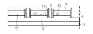
図1Aは、オプトエレクトロニクス半導体部品を製造する方法の第1の段階を示す。ここで、半導体積層体1が、例えば半導体積層体1の成長基板などの基板13に直接載置される。半導体積層体1は、基板13に対向する第1の主面と、基板13とは反対側に面する第2の主面とを有する。第1の層10と、活性層11と、第2の層12とが、基板13に配置され、特定の順序で第1の主面と第2の主面との間に載置される。さらに、第2のコンタクト層320とその上に配置される第1のパッシベーション層14とが半導体積層体1の第2の主面に載置される。
FIG. 1A shows a first step in a method for manufacturing an optoelectronic semiconductor component. Here, the
半導体積層体1は、例えばGaN系であり、基板13は、例えばサファイアまたはGaN成長基板である。第2のコンタクト層320は、例えばAgから形成されている。第1のパッシベーション層14は、SiO2またはSiNなどの絶縁性材料を含む、またはこれらからなる。
The
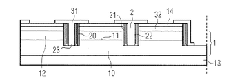
図1Bに示す製造する方法の段階では、第2のコンタクト層320およびその上に配置されたパッシベーション層14は、マスクを用いたリソグラフィによってパターン化される。このような構造化によって、第2のコンタクト要素32は、第2の主面において、活性層11の主延在方向に平行である側方に互いに離間して配置される。
1B, the
図1Cに示す段階で、半導体積層体1は、同じマスクを用いてパターン化される。ここで、第2の主面から第2の層12および活性層11を完全に貫通して延在し、第1の層10に開口する凹部2が、半導体積層体1に導入される。凹部2は、隣接する第2のコンタクト要素32の間の空間に形成される。凹部2は、円柱状の貫通孔または溝であり、それぞれ活性層11を横切って延在する側面と、活性層11と実質的に平行な底面とを有している。
At the stage shown in FIG. 1C, the
図1Dの段階において、SiO2層またはSiN層などの第1の絶縁層20の形態である第1の中間層20が、凹部2の側壁に全面的に載置される。第1の絶縁層20は例えば、まず第1の絶縁層20のコンフォーマル堆積(conformal deposition)によって、半導体積層体1の第2の主面に載置されうる。ここで第1の絶縁層20は、凹部2の側壁および底面にぴったりと配置される。その後、第2の主面に垂直な面におけるよりも第2の主面に平行な面におけるエッチング速度が大きい、乾式化学エッチングバックプロセスが行われる。この結果、第1の絶縁層20は、凹部2の底面から完全に除去される一方、凹部2の側面に残る。このような自己整合エッチングバックプロセスでは、リソグラフィマスクのようにマスクの使用を必要としない。
In the stage of FIG. 1D, a first
図1Eに示す段階では、例えばAg層などの第1の金属ミラー層21が、第2の主面から半導体積層体1に載置される。第1のミラー層21は、凹部2の底面および側壁の両方を完全にぴったりと覆う。
At the stage shown in FIG. 1E, a first
図1Fの段階では、例えばSiO2層またはSiN層などの第2の絶縁層22が、凹部2の側壁の領域において第1の金属ミラー層21に載置される。第2の絶縁層22の載置は、第1の絶縁層20の載置と同様に、コンフォーマル堆積の後に、エッチングバックプロセスによって行われる。このように、凹部2の底面の領域に配置された第1の金属ミラー層21から第2の絶縁層22が除去される。
In the stage of FIG. 1F, a second insulating
図1Gの段階において、凹部2の底面から第1の金属ミラー層21も除去される。凹部2の底面から第1の金属ミラー層21を除去するために、乾式化学または湿式化学エッチングが用いられうる。湿式化学エッチング、特に等方性エッチングの場合、側壁において第1のミラー層21に影響が及ばないように、第2の絶縁層22が側壁上で保護層として機能する。したがって、第2の絶縁層22は、第1の金属ミラー層21にエッチングプロセスを行うためのマスクとして実質的に機能する。凹部2の底面から第1の金属ミラー層21をエッチング除去するために、追加のリソグラフィマスクの使用も必要でない。
1G, the first
図1Hの段階では、凹部2は、Al、Ti、またはAuなどの金属材料の形態である金属注入要素23で充填される。第2の主面において、金属注入要素23は、凹部2の周りの領域も覆う。図1Hの断面図では、金属注入要素23は、T形状である。概して、第1のコンタクト要素31は、凹部2を完全に充填する金属注入要素23で少なくとも部分的に充填することで形成される。凹部2の底面の領域において、金属注入要素23は、半導体積層体1の第1の層10と直接接触する。あるいは、第1の層10および金属注入要素23と直接接触するZnOまたはITOなどの透明導電性材料が凹部2の底面に載置される。
In the stage of FIG. 1H, the
図1Iに示す段階で、第2のパッシベーション層15が第2の主面に載置され、第1のコンタクト要素31および第2のコンタクト要素32を完全にぴったりと覆う。第2のパッシベーション層15は、第1のパッシベーション層14と同じ材料を含む、または同じ材料からなる。
At the stage shown in FIG. 1I, a
図1Jにおいて、第1のパッシベーション層14および第2のパッシベーション層15がリソグラフィでパターン化され、第1のコンタクト要素31および第2のコンタクト要素32が、少なくとも部分的に露出する。特に、第2のコンタクト要素32は、第1のコンタクト要素31と重ならない領域で露出する。
In FIG. 1J, first and second passivation layers 14 and 15 are lithographically patterned, exposing first and
図1Kの段階では、図示のスイッチ50を含むキャリア5が、半導体積層体1の第2の主面に載置される。ここで、スイッチ50は、はんだ金属または導電性接着剤などの導電性材料を介して機械的および導電的に第2のコンタクト要素32に接続される。第2のコンタクト要素32は、各スイッチ50に個別に割り当てられている。スイッチ50を介して、個々の第2のコンタクト要素32は個別に、互いに独立して接続、または電圧印加される。さらに、第1のコンタクト要素31には、全ての第1のコンタクト要素31に共に接続して電流を供給する共通のスイッチ50が割り当てられている。
At the stage of FIG. 1K, the
図1Kでは、基板13が半導体積層体1の第1の主面から除去されていることもわかる。半導体積層体1の第1の主面は、活性層11で発せられる放射のための放射面6を形成している。放射面6は、複数の第1のコンタクト要素31および第2のコンタクト要素32にわたって連続して延在している。
FIG. 1K also shows that the
さらに図1Kから、像点4は、各第2のコンタクト要素32に個別に割り当てられていることが分かる。動作時に放射面6を見たときに、どの第2のコンタクト要素32に電流が供給されるかに応じて、像点4が明るくなる。像点4は、第2のコンタクト要素32の放射面6への投影で実質的に規定される。したがって像点4の形状、大きさおよび位置は、第2コンタクト要素32の形状、大きさおよび位置に実質的に基づいている。
Furthermore, it can be seen from FIG. 1K that the image points 4 are individually assigned to each
図1Lは、上記半導体部品100の例示的な一実施形態を、半導体積層体1の第2の主面の平面図で示す。個々の第2のコンタクト要素32がマトリクス状パターンに配置されていることがわかる。第1のコンタクト要素31は、単一の連続する第1のコンタクト要素31を形成している。凹部2は、第2のコンタクト要素32の周りに格子の形態で配置された連続する溝2を形成している。第1のコンタクト要素31は、複数の第2のコンタクト要素32に対する共通の嵌合接触部を形成している。
FIG. 1L shows an exemplary embodiment of the
図1Mは、半導体部品100の第1の主面または放射面6の平面図を示す。第2のコンタクト要素32に個別に割り当てられている個々の像点4の輪郭は、破線で示されており、これらの輪郭は、第2のコンタクト要素32の輪郭に実質的に対応する。個々の像点4は、図1Mに示す放射面6がピクセル化発光面となるように、動作時に個々に、互いに独立して制御されうる。
FIG. 1M is a plan view of the first main surface or the
図1Lの例示的な実施形態のように、図1Nの例示的な実施形態において、半導体積層体1の第2の主面の平面図が示されている。図1Lとは対照的に、ここで凹部は第2のコンタクト要素32の周りの溝2としては配置されず、半導体積層体1の穴2として形成されている。穴2はそれぞれ、第2のコンタクト要素32の周りの格子網の交点に設けられている。特に、穴2に配置されている第1のコンタクト要素31はしたがって、例えば半導体積層体1に形成された円柱状の貫通孔などの、めっき貫通孔の形態である。複数の第1のコンタクト要素31は、各第2のコンタクト要素32と関連づけられる。しかしながら少なくとも2つの第2のコンタクト要素32が、各第1のコンタクト要素31に割り当てられる。
Like the exemplary embodiment of FIG. 1L, in the exemplary embodiment of FIG. 1N, a plan view of the second main surface of the
図2Aから2Cは、図1Aおよび1Bの工程とは別の工程を示す。 2A to 2C show a step different from the steps of FIGS. 1A and 1B.
図2Aでは、互いに隔てられた複数の第2のコンタクト要素32が半導体積層体1の第2の主面に載置される。図1Aの段階とは対照的に、この時点で第1のパッシベーション層14は、第2のコンタクト要素32に載置されていない。
In FIG. 2A, a plurality of
図2Bの段階では、第1のパッシベーション層14は、第2のコンタクト要素32に載置される。ここで、第1のパッシベーション層14は、第2のコンタクト要素32を完全に覆い、隣接する第2のコンタクト要素32の間で第2の主面の中間領域を充填している。
At the stage of FIG. 2B, the
第1のパッシベーション層14はその後、半導体積層体1が2つの隣接する第2のコンタクト要素32の間の領域で露出するように、マスクを用いたピクセルレベルの微細リソグラフィによってパターン化されうる。図2Cはその結果を示している。図1Bとは対照的に、これらの工程で、第2のコンタクト要素32は、第2の主面を横切って延在する側面においても、第1のパッシベーション層14で覆われている。これによって、第2のコンタクト要素32がより好適に保護されるという利点がある一方、第2のコンタクト要素32間の領域の面積がさらに減り、さらなる処理工程が必要になるという欠点がある。
The
図3Aから3Bは、図1Hから1Jの工程とは別の工程を示す。ここで図3Aは、図1Hに対応している。 3A to 3B show a step different from the steps of FIGS. 1H to 1J. Here, FIG. 3A corresponds to FIG. 1H.
図1Hから1Jの例示的な実施形態とは異なり、第1のコンタクト要素31が形成された後、第2のパッシベーション層15は、半導体積層体1の第2の主面に載置されない。その代わりに、図3Bに示すように、第1のパッシベーション層14は、フォトリソグラフィによって直接パターン化され、第1のコンタクト要素31および第2のコンタクト要素32は、少なくとも部分的に露出される。第2のパッシベーション層15は、全く用いられない。このため、図1に示した方法より必要な工程が少なく有利である。
Unlike the exemplary embodiment of FIGS. 1H to 1J, after the
図4Aから4Cは、図1Eから1Hの工程とは別の工程を示す。ここで図4Aは、図1Eに対応している。 4A to 4C show another step different from the steps of FIGS. 1E to 1H. Here, FIG. 4A corresponds to FIG. 1E.
図1Eから1Hとは対照的に、凹部2の底面から第1の金属ミラー層21を除去するために第2の絶縁層22は用いられない。その代わりに図4Bに示すように、第1の金属ミラー層21は、凹部2の底面から、例えば乾式化学エッチングバックプロセスなどの異方性エッチングバックプロセスによってエッチングバックされる。エッチングバックプロセスにおける異方性のために、凹部2の底面のみが露出され、第1の金属ミラー層21は凹部2の側壁に残る。
1E to 1H, no second insulating
図4Cは、どのように凹部2が金属注入要素23で充填されるかを示しており、この結果、第1のコンタクト要素31が形成される。さらに、金属注入要素23は凹部2の底面で第1の層10と直接接触している。また、図4Cの例示的な実施形態では、金属注入要素23は、第1のミラー層21とも直接電気接触している。
FIG. 4C shows how the
図5Aから5Cでは、図1Dから1Hの工程の代替として行われうる工程の段階が示されている。 5A to 5C show process steps that can be performed as an alternative to the processes of FIGS. 1D to 1H.
図5Aは、上記図1Dに対応する。つまり、凹部2の側壁はすでに第1の絶縁層20で覆われており、これに対して凹部2の底面に第1の絶縁層20は存在しない。
FIG. 5A corresponds to FIG. 1D described above. That is, the side wall of the
図5Bは、どのように金属注入要素23が底面に層として、例えば物理気相成長(略してPVD)などの異方性堆積法によって、凹部2の底面に直接載置されるかを示している。これは、例えばフォトリソグラフィマスクを用いることで行われうる。異方性堆積法を用いることで、凹部2の側面には金属注入要素23が存在しないままである。
FIG. 5B shows how the
図5Cに示す段階では、その後、反射性金属充填材料21が凹部2に導入される。充填材料21は、凹部2を完全に充填し、第2の主面から離れる方向に凹部2から突出している。反射性充填材料21は同時に、第1の金属ミラー層21を形成している。上記例示的な実施形態とは対照的に、第1のコンタクト要素31は、注入要素23の代わりに、第1の金属ミラー層21から主に形成されている。
At the stage shown in FIG. 5C, the reflective
図6Aは、図1Kの例示的な実施形態に対応する、オプトエレクトロニクス半導体部品100の例示的な一実施形態の側面図である。また、図6Aは、活性層11で発生する電磁波の光路を矢印で示している。
FIG. 6A is a side view of one exemplary embodiment of the
実線の矢印は、活性層11から直接、放射面6を介して半導体部品100から出射される、像点4内の光線を示している。
Solid arrows indicate light rays in the image point 4 that are emitted from the
破線の矢印は、光線が凹部の側壁で反射された後、放射面を介して出射される光路を示している。ここで、光線は、高反射性である第1の金属ミラー層21によって特に効果的に反射される。
The dashed arrows indicate the path of the light rays exiting through the radiating surface after the light rays are reflected by the side walls of the recess. Here, the light rays are reflected particularly effectively by the highly reflective first
点線の矢印は、活性層11からの光線がまず放射面6に当たって、フレネル反射または全反射によって部分的または完全に反射される光路を示している。このような光線は、隣接する像点4に到達し、ピクセル間のコントラストを低下するおそれがある。
The dotted arrows indicate the optical path in which the light rays from the
しかしながら、例示的な本実施形態では、光線はまず凹部2の底面、第1の金属ミラー層21ではなく金属注入要素23に当たる。金属注入要素23は、光が底面で吸収されるように、吸収性または反射しにくいことが好ましい。これによって隣接する像点4の光クロストークが低減され、観察者に対するコントラスト比が高められる。
However, in the exemplary embodiment, the light beam first strikes the bottom surface of the
これとは対照的に、図6Bは、金属注入要素23と第1の金属ミラー層21とが同じ材料で形成された半導体部品100の変形例を示す。図6Bから理解されるように、光線は凹部2の底面で反射され、隣接する像点のクロストークが生じて、観察者に対するコントラスト比が低下する。
In contrast, FIG. 6B shows a variant of the
図7Aから7Dは、製造方法のさらなる例示的な実施形態における様々な段階を示している。図7Aの段階は、例えば図1Cの段階に続くものである。 7A to 7D show various stages in a further exemplary embodiment of the manufacturing method. The stage of FIG. 7A follows, for example, the stage of FIG. 1C.
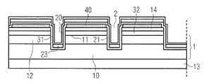
図7Aでは、凹部2の領域に開口を有するフォトマスク40がパッシベーション層14にさらに載置される。概して、このような開口は、凹部2の側方への広がりより大きい。図7Aに示すように、第1の透明中間層20が、例えばスパッタリングなどの無方向性(undirected)プロセスによって、連続する層としてフォトマスク40に載置され、凹部2に導入される。ここで、第1の透明中間層20は、凹部2の底面および側壁の両方を完全に覆う。
In FIG. 7A, a
上記例示的な実施形態とは対照的に、第1の透明中間層20は第1の絶縁層ではなく、半導体積層体1の第1の層10とのコンタクト抵抗が低く、半導体積層体1の第2の層12とのコンタクト抵抗が高いコンタクト層20である。半導体積層体1は例えば、GaN系であり、第1の層10は、例えばn−GaN層であり、第2の層12は、例えばp−GaN層である。コンタクト層20の材料は、例えばZnOである。
In contrast to the exemplary embodiment described above, the first transparent
上記例示的な実施形態の全てにおいて、第1の透明中間層20は第1の絶縁層20であったが、第1の絶縁層20はそれぞれこのようなコンタクト層20にも置き換えることが可能である。
In all of the above-described exemplary embodiments, the first transparent
図7Bの段階において、金属層が、気相蒸着などの方向性プロセスによってコンタクト層20に載置される。このような金属層は、凹部2の底面の領域において金属注入要素23を形成する。コンタクト層20は、金属注入要素23と第1の層10との間で電流を伝導しうる。金属層の方向性載置によって、側方に延在する面、特に底面のみが確実に覆われる。垂直に延在する面、特に側壁は、金属注入要素23の金属材料で覆われない、またはわずかにのみ覆われる。
At the stage of FIG. 7B, a metal layer is placed on the
図7Cの段階では、第1の金属ミラー層21は、側壁および底面の両方が第1の金属ミラー層21で覆われるように、無方向性または等方性の方法で載置される。
In the stage of FIG. 7C, the first
図5Cの例示的な実施形態の例とは対照的に、第1の金属ミラー層21は、凹部2を完全には充填せず、凹部2の底面および側壁に沿って部分的にのみ充填する。ここで凹部2の一部は充填されないままである。このような凹部2の部分的な充填は、上記例示的な実施形態の全てにおいても選択しうる。
In contrast to the example of the exemplary embodiment of FIG. 5C, the first
図7Dは、フォトマスク40がその上に位置する層と共に分離された段階を示す。その後、例えば図1Iから1Kに関連して説明した工程が、半導体部品100を完成するために行われうる。
FIG. 7D shows the stage in which the
本発明は例示的な実施形態を用いた説明に限定されない。むしろ本発明はいかなる新たな特徴およびいかなる特徴の組み合わせを包含し、たとえこれらの特徴またはその組み合わせ自体が本願特許請求項または例示的な実施形態に明示的に記述されていなくても、本発明は特に本願特許請求項におけるいかなる特徴の組み合わせも包含する。 The invention is not limited to the description using the exemplary embodiments. Rather, the invention includes any novel features and any combination of features that may be present even if these features or combinations thereof are not explicitly recited in the claims or exemplary embodiments. In particular, it includes any combination of features in the claims of the present application.
本出願は、独国特許出願第102015119353.1号の優先権を主張するものであり、この文書の開示内容は参照により本明細書に援用される。 This application claims the benefit of German Patent Application No. 102015119353.1, the disclosure of which is incorporated herein by reference.
1 半導体積層体
2 凹部
4 像点
5 キャリア
6 放射面
10 第1の層
11 活性層
12 第2の層
13 基板
14 第1のパッシベーション層
15 第2のパッシベーション層
20 第1の透明中間層
21 第1の金属ミラー層
22 第2の絶縁層
23 金属注入要素
31 第1のコンタクト要素
32 第2のコンタクト要素
40 フォトマスク
50 スイッチ
100 オプトエレクトロニクス半導体部品
DESCRIPTION OF
Claims (20)
前記第2の主面に配置され、前記半導体積層体(1)において前記第2の主面から前記第2の層(12)および前記活性層(11)を完全に貫通して延在して前記第1の層(10)に開口している凹部(2)を充填している第1のコンタクト要素(31)と、
前記第2の主面に平行で、かつ、横方向に互いに離間して前記第2の主面に設けられ、前記第2の主面の平面視において、前記凹部(2)に隣接して側方に配置されている複数の第2のコンタクト要素(32)と、
を備えるオプトエレクトロニクス半導体部品(100)であって、
前記第1のコンタクト要素(31)は、第1の透明中間層(20)と、第1の金属ミラー層(21)と、金属注入要素(23)とを含み、
前記第1の透明中間層(20)は、前記活性層(11)を横切って延びる前記凹部(2)の側壁に配置され、前記半導体積層体(1)に直接接触し、
前記第1の金属ミラー層(21)は、前記側壁の領域において前記第1の透明中間層(20)に直接設けられ、
前記金属注入要素(23)は、前記第1の層(10)に直接隣接する前記凹部(2)の底面に配置され、前記金属注入要素(23)と前記底面との間に更なる金属要素は配置されておらず、
前記第1の層(10)の領域において、前記第1の層(10)と前記第1の金属ミラー層(21)との間に電気的接触が生成され、
前記第1の透明中間層(20)は、動作中に、前記第2の層(12)と前記第1のコンタクト要素(31)との間に直接電流が流れることを防止し、
前記第2のコンタクト要素(32)の輪郭は、動作中に前記第1の主面を見たときに明るくなる前記半導体部品(100)の像点(4)の形状、大きさおよび位置を規定し、
前記金属注入要素(23)および前記第1の金属ミラー層(21)は、異なる材料組成を有し、
前記第2のコンタクト要素(32)はそれぞれ、像点(4)に個別に割り当てられる、
オプトエレクトロニクス半導体部品(100)。 Including a first main surface, a first layer (10), an active layer (11), a second layer (12), and a second main surface, arranged one above the other in a specific order. A semiconductor laminate (1);
Being disposed on the second main surface and extending completely through the second layer (12) and the active layer (11) from the second main surface in the semiconductor laminate (1). A first contact element (31) filling a recess (2) opening in said first layer (10);
The second main surface is provided on the second main surface in parallel with the second main surface and spaced apart from each other in the lateral direction, and is adjacent to the recess (2) in a plan view of the second main surface. A plurality of second contact elements (32) disposed toward
A Ru comprising an optoelectronic semiconductor component (100),
The first contact element (31) includes a first transparent intermediate layer (20), a first metal mirror layer (21), and a metal injection element (23);
The first transparent intermediate layer (20) is disposed on a side wall of the recess (2) extending across the active layer (11), and directly contacts the semiconductor laminate (1);
The first metal mirror layer (21) is provided directly on the first transparent intermediate layer (20) in the region of the side wall;
The metal injection element (23) is arranged on the bottom surface of the recess (2) directly adjacent to the first layer (10), and further metal elements between the metal injection element (23) and the bottom surface Is not located,
In the region of the first layer (10), an electrical contact is created between the first layer (10) and the first metal mirror layer (21);
The first transparent intermediate layer (20) prevents a current from flowing directly between the second layer (12) and the first contact element (31) during operation;
The contour of the second contact element (32) defines the shape, size and position of the image point (4) of the semiconductor component (100) that becomes bright when looking at the first main surface during operation. And
The metal injection element (23) and the first metal mirror layer (21) have different material compositions;
The second contact elements (32) are each individually assigned to an image point (4);
Optoelectronic semiconductor components (100).
前記活性層(11)によって出射される平均波長における前記第1の金属ミラー層(21)の反射率は、少なくとも80%であり、
前記活性層(11)によって出射される平均波長における前記金属注入要素(23)の反射率は、多くとも50%である、
請求項1に記載のオプトエレクトロニクス半導体部品(100)。 At least 80% or more of the side wall of the recess (2) is covered by the first metal mirror layer (21);
The reflectivity of the first metal mirror layer (21) at the average wavelength emitted by the active layer (11) is at least 80%;
The reflectivity of the metal injection element (23) at the average wavelength emitted by the active layer (11) is at most 50%;
An optoelectronic semiconductor component (100) according to claim 1.
前記底面の領域において、前記金属注入要素(23)と前記第1の層(10)との間に透明層が配置され、前記透明層は、前記金属注入要素(23)および前記第1の層(10)と直接接続されており、前記活性層(11)によって出射される平均波長において少なくとも80%の透明度を有する、
請求項1または2に記載のオプトエレクトロニクス半導体部品(100)。 The metal injection element (23) is directly adjacent to the first layer (10) in the region of the bottom surface, or
In the region of the bottom surface, a transparent layer is arranged between the metal injection element (23) and the first layer (10), the transparent layer comprising the metal injection element (23) and the first layer (10) and has a transparency of at least 80% at an average wavelength emitted by the active layer (11);
Optoelectronic semiconductor component (100) according to claim 1 or 2.
請求項1から3の何れか1項に記載のオプトエレクトロニクス半導体部品(100)。 The first transparent intermediate layer (20) is a first insulating layer (20) and is located between the first metal mirror layer (21) and the semiconductor laminate (1) in the region of the side wall. Preventing direct current flow,
An optoelectronic semiconductor component (100) according to any one of the preceding claims.
前記コンタクト層(20)は、前記第1の層(10)の領域において、前記第1の層(10)と前記第1の金属ミラー層(21)との間に電気的接触を生成し、
前記コンタクト層(20)は、前記第2の層(12)の領域において、前記第1の金属ミラー層(21)と前記第2の層(12)との間で電気絶縁的に作用し、
前記コンタクト層(20)は、前記底面と前記金属注入要素(23)との間に追加的に配置されている、
請求項1から4の何れか1項に記載のオプトエレクトロニクス半導体部品(100)。 The first transparent intermediate layer (20) is a contact layer (20);
The contact layer (20) creates an electrical contact between the first layer (10) and the first metal mirror layer (21) in the region of the first layer (10);
The contact layer (20) electrically acts between the first metal mirror layer (21) and the second layer (12) in a region of the second layer (12),
The contact layer (20) is additionally arranged between the bottom surface and the metal injection element (23);
An optoelectronic semiconductor component (100) according to any one of the preceding claims.
前記活性層(11)は、前記活性層(11)上に前記第2のコンタクト要素(32)を投影させた領域に連続的に形成されている、
請求項1から5の何れか1項に記載のオプトエレクトロニクス半導体部品(100)。 Said second contact element (32) is formed continuously;
The active layer (11) is continuously formed on a region where the second contact element (32) is projected on the active layer (11).
An optoelectronic semiconductor component (100) according to any one of the preceding claims.
前記凹部(2)は、2つの隣接する第2のコンタクト要素(32)の間の領域に配置される、
請求項1から6の何れか1項に記載のオプトエレクトロニクス半導体部品(100)。 The second contact elements (32) are controlled independently of each other during operation such that the image points (4) are brightened independently of each other;
Said recess (2) is arranged in a region between two adjacent second contact elements (32);
Optoelectronic semiconductor component (100) according to any of the preceding claims.
請求項1から7の何れか1項に記載のオプトエレクトロニクス半導体部品(100)。 At least one image point (4) is assigned a plurality of first contact elements (31) overlappingly contacting each image point (4);
An optoelectronic semiconductor component (100) according to any of the preceding claims.
請求項1から8の何れか1項に記載のオプトエレクトロニクス半導体部品(100)。 At least one of said first contact elements (31) is arranged laterally adjacent to a plurality of adjacent image points (4) and simultaneously to contact said plurality of adjacent image points (4). It is formed,
Optoelectronic semiconductor component (100) according to any of the preceding claims.
少なくとも1つの第1のコンタクト要素(31)の少なくとも1つの凹部(2)は、前記格子網の少なくとも1つの交点に配置される、
請求項7に記載のオプトエレクトロニクス半導体部品(100)。 Said image points (4) are arranged in a grid mesh,
At least one recess (2) of at least one first contact element (31) is arranged at at least one intersection of said grid network;
An optoelectronic semiconductor component (100) according to claim 7.
前記溝(2)および前記金属注入要素(23)はそれぞれ、前記第2の主面の平面視において、前記第2のコンタクト要素(32)を完全に囲む連続軌道を形成する、
請求項1から10の何れか1項に記載のオプトエレクトロニクス半導体部品(100)。 The recess (2) is formed as a groove (2),
The groove (2) and the metal injection element (23) each form a continuous track that completely surrounds the second contact element (32) in plan view of the second main surface.
An optoelectronic semiconductor component (100) according to any one of the preceding claims.
連続的な前記溝(2)には、動作中に複数の像点(4)に同時に接触する単一の連続的な第1のコンタクト要素(31)が形成される、
請求項7または11に記載のオプトエレクトロニクス半導体部品(100)。 Said grooves (2) are connected around individual said second contact elements (32), forming a grid around said second contact elements (32);
In said continuous groove (2) is formed a single continuous first contact element (31) which simultaneously contacts a plurality of image points (4) during operation;
Optoelectronic semiconductor component (100) according to claim 7 or 11.
請求項12に記載のオプトエレクトロニクス半導体部品(100)。 Between the metal injection element (23) and the first metal mirror layer (21), a second insulating layer (22) is arranged in the region of the side wall of the recess (2),
Optoelectronic semiconductor component (100) according to claim 12.
前記第1の金属ミラー層は、反射性充填材料として前記凹部(2)に導入され、前記金属注入要素(23)と前記第2の主面との間の領域を完全にまたは少なくとも部分的に充填する、
請求項1から13の何れか1項に記載のオプトエレクトロニクス半導体部品(100)。 The metal injection element (23) is provided as a layer on the bottom surface of the recess (2);
The first metal mirror layer is introduced into the recess (2) as a reflective filling material to completely or at least partially fill the area between the metal injection element (23) and the second major surface. Filling,
An optoelectronic semiconductor component (100) according to any one of the preceding claims.
B)前記第2の主面において、前記活性層の主延在方向に平行である側方に互いに離間して配置されるように、複数の第2のコンタクト要素(32)を設ける工程と、
C)前記第2の層(12)および前記活性層(11)を完全に貫通して前記第1の層(10)に開口し、前記第2の主面の平面視において、前記第2のコンタクト要素(32)に隣接して側方に配置される凹部(2)を、前記第2の主面から前記半導体積層体(1)の中に穴または溝の形態で導入する工程と、
D)第1の透明中間層(20)が前記半導体積層体(1)に直接隣接するように、前記活性層(11)に対して側方に延びる前記凹部(2)の底面および側壁の全領域に前記第1の透明中間層(20)を設け、続いて、自己整合エッチングバックプロセスによって前記底面から前記第1の透明中間層(20)が除去される工程と、
E)前記側壁の領域において、第1の金属ミラー層(21)を前記第1の透明中間層(20)に直接設ける工程と、
F)前記第1の層(10)に直接隣接する前記凹部(2)の前記底面に金属注入要素(23)を設ける工程と、
を含み、
前記金属注入要素(23)と前記底面との間に更なる金属要素は配置されておらず、
前記金属注入要素(23)および前記第1の金属ミラー層(21)は、異なる材料組成を有する、
オプトエレクトロニクス半導体部品(100)の製造方法。 A) A first main surface, a first layer (10) on the first main surface, an active layer (11) on the first layer (10), and on the active layer (11). Providing a semiconductor laminate (1) having a second layer (12) and a second main surface on the second layer (12);
B) providing a plurality of second contact elements (32) on the second main surface so as to be spaced apart from each other on a side parallel to a main extending direction of the active layer;
C) completely penetrating the second layer (12) and the active layer (11) to open an opening in the first layer (10), and in plan view of the second main surface, the second layer Introducing a recess (2) arranged laterally adjacent to the contact element (32) from the second main surface into the semiconductor stack (1) in the form of a hole or a groove;
D) the entire bottom and side walls of the recess (2) extending laterally with respect to the active layer (11) such that the first transparent intermediate layer (20) is directly adjacent to the semiconductor stack (1). wherein the region first transparent intermediate layer (20) is provided, followed by a step of the from the bottom surface by a self aligned etch back process first transparent intermediate layer (20) is Ru is removed,
E) providing a first metal mirror layer (21) directly on the first transparent intermediate layer (20) in the region of the side wall;
F) providing a metal injection element (23) on the bottom surface of the recess (2) directly adjacent to the first layer (10);
Including
No further metal element is arranged between the metal injection element (23) and the bottom surface;
The metal injection element (23) and the first metal mirror layer (21) have different material compositions;
A method for manufacturing an optoelectronic semiconductor component (100).
乾式化学エッチバックプロセスによって前記底面から前記第1の透明中間層(20)が除去され、
前記第1の透明中間層(20)の前記エッチバックプロセスは、リソグラフィマスクを使用せずに実行される、
請求項15に記載のオプトエレクトロニクス半導体部品(100)の製造方法。 In step D),
Wherein from said bottom surface by dry type chemical etch-back process first transparent intermediate layer (20) is removed,
The etch-back process of the first transparent intermediate layer (20) is performed without the use of Li source graphic mask,
A method for producing an optoelectronic semiconductor component (100) according to claim 15.
前記第1の層(10)の領域において、前記第1の層(10)と前記第1の金属ミラー層(21)との間に電気的接触が生成される、
請求項15または16に記載のオプトエレクトロニクス半導体部品(100)の製造方法。 In step D),
In the region of the first layer (10), an electrical contact is created between the first layer (10) and the first metal mirror layer (21),
A method for producing an optoelectronic semiconductor component (100) according to claim 15 or 16 .
前記第1の金属ミラー層(21)は、前記凹部(2)の前記底面および前記側壁の全領域に設けられ、
続いて、湿式化学または乾式化学エッチバックプロセスによって前記底面から前記第1の金属ミラー層(21)が除去され、
前記第1の金属ミラー層(21)の前記エッチバックプロセスは、自己整合的であり、リソグラフィマスクを使用せずに実行される、
請求項15から17の何れか1項に記載のオプトエレクトロニクス半導体部品(100)の製造方法。 In step E),
The first metal mirror layer (21) is provided on the entire bottom surface and the side wall of the concave portion (2),
Subsequently, the first metal mirror layer (21) is removed from the bottom surface by a wet chemical or dry chemical etchback process,
The etch-back process of the first metal mirror layer (21) is self-aligned and performed without using a lithographic mask;
A method for manufacturing an optoelectronic semiconductor component (100) according to any one of claims 15 to 17.
第2の絶縁層(22)が、前記凹部(2)の前記底面および前記側壁の領域において、前記第1の金属ミラー層(21)の全領域に設けられ、
続いて、乾式化学エッチバックプロセスによって、前記底面の領域において前記第1の金属ミラー層(21)から前記第2の絶縁層(22)が除去され、
前記第2の絶縁層(22)の前記エッチバックプロセスは、自己整合的であり、リソグラフィマスクを使用せずに実行される、
請求項18に記載のオプトエレクトロニクス半導体部品(100)の製造方法。 After providing the first metal mirror layer (21) and before the etch-back process of the first metal mirror layer (21),
A second insulating layer (22) is provided over the entire area of the first metal mirror layer (21) in the area of the bottom surface and the side wall of the recess (2);
Subsequently, the second insulating layer (22) is removed from the first metal mirror layer (21) in the region of the bottom surface by a dry chemical etchback process,
The etch-back process of the second insulating layer (22) is self-aligned and performed without using a lithographic mask;
Method for manufacturing an optoelectronic semiconductor component (100) according to claim 18.
工程F)において、前記金属注入要素(23)は、異方性堆積法によって前記凹部(2)の前記底面上に層として形成され、
工程E)において、前記凹部(2)は、前記第1の金属ミラー層(21)を形成する反射性材料で充填される、
請求項15から17の何れか1項に記載のオプトエレクトロニクス半導体部品(100)の製造方法。 Step F) is performed before Step E),
In step F), said metal injection element (23) is formed as a layer on said bottom surface of said recess (2) by anisotropic deposition method,
In step E), said recess (2) is filled with a reflective material forming said first metal mirror layer (21),
A method for manufacturing an optoelectronic semiconductor component (100) according to any one of claims 15 to 17.
Applications Claiming Priority (3)
| Application Number | Priority Date | Filing Date | Title |
|---|---|---|---|
| DE102015119353.1 | 2015-11-10 | ||
| DE102015119353.1A DE102015119353B4 (en) | 2015-11-10 | 2015-11-10 | Optoelectronic semiconductor component and method for producing an optoelectronic semiconductor component |
| PCT/EP2016/077149 WO2017081085A1 (en) | 2015-11-10 | 2016-11-09 | Optoelectronic semiconductor component and method for producing an optoelectronic semiconductor component |
Publications (2)
| Publication Number | Publication Date |
|---|---|
| JP2018533220A JP2018533220A (en) | 2018-11-08 |
| JP6661009B2 true JP6661009B2 (en) | 2020-03-11 |
Family
ID=57249827
Family Applications (1)
| Application Number | Title | Priority Date | Filing Date |
|---|---|---|---|
| JP2018521031A Active JP6661009B2 (en) | 2015-11-10 | 2016-11-09 | Optoelectronic semiconductor component and method of manufacturing optoelectronic semiconductor component |
Country Status (5)
| Country | Link |
|---|---|
| US (1) | US10374121B2 (en) |
| JP (1) | JP6661009B2 (en) |
| CN (1) | CN108292696B (en) |
| DE (1) | DE102015119353B4 (en) |
| WO (1) | WO2017081085A1 (en) |
Families Citing this family (42)
| Publication number | Priority date | Publication date | Assignee | Title |
|---|---|---|---|---|
| DE102017117414A1 (en) * | 2017-08-01 | 2019-02-07 | Osram Opto Semiconductors Gmbh | Method for producing an optoelectronic component and optoelectronic component |
| FR3073669B1 (en) * | 2017-11-10 | 2021-11-05 | Commissariat Energie Atomique | METHOD OF MANUFACTURING AN OPTOELECTRONIC DEVICE INCLUDING A PLURALITY OF DIODES |
| US11749790B2 (en) * | 2017-12-20 | 2023-09-05 | Lumileds Llc | Segmented LED with embedded transistors |
| FR3076170B1 (en) * | 2017-12-22 | 2020-05-15 | Commissariat A L'energie Atomique Et Aux Energies Alternatives | METHOD FOR DEFERRING ELECTROLUMINESCENT STRUCTURES |
| DE102019101544A1 (en) | 2018-01-24 | 2019-07-25 | Osram Opto Semiconductors Gmbh | Optoelectronic component and method |
| DE102018106970A1 (en) | 2018-03-23 | 2019-09-26 | Osram Opto Semiconductors Gmbh | Optoelectronic semiconductor component and method for producing an optoelectronic semiconductor component |
| US10615305B1 (en) * | 2018-04-20 | 2020-04-07 | Facebook Technologies, Llc | Self-alignment of micro light emitting diode using planarization |
| JP7105612B2 (en) * | 2018-05-21 | 2022-07-25 | シャープ株式会社 | IMAGE DISPLAY DEVICE AND METHOD OF FORMING THE SAME |
| DE102018122492A1 (en) * | 2018-09-14 | 2020-03-19 | Osram Opto Semiconductors Gmbh | OPTOELECTRONIC SEMICONDUCTOR COMPONENT WITH A FIRST AND SECOND METAL LAYER AND METHOD FOR PRODUCING THE OPTOELECTRONIC SEMICONDUCTOR COMPONENT |
| FR3087580B1 (en) * | 2018-10-23 | 2020-12-18 | Aledia | PROCESS FOR MAKING AN OPTOELECTRONIC DEVICE INCLUDING LIGHT DIODES HOMOGENOUS IN DIMENSIONS |
| JPWO2020100303A1 (en) * | 2018-11-16 | 2021-10-07 | 堺ディスプレイプロダクト株式会社 | Micro LED device and its manufacturing method |
| WO2020100299A1 (en) * | 2018-11-16 | 2020-05-22 | 堺ディスプレイプロダクト株式会社 | Micro led device and method for manufacturing same |
| US20210358998A1 (en) * | 2018-11-16 | 2021-11-18 | Sakai Display Products Corporation | Micro led device and production method therefor |
| US20220013511A1 (en) * | 2018-11-16 | 2022-01-13 | Sakai Display Products Corporation | Micro led device and method for manufacturing same |
| WO2020100300A1 (en) * | 2018-11-16 | 2020-05-22 | 堺ディスプレイプロダクト株式会社 | Micro led device and method for manufacturing same |
| WO2020100290A1 (en) * | 2018-11-16 | 2020-05-22 | 堺ディスプレイプロダクト株式会社 | Micro led device and production method therefor |
| JPWO2020100292A1 (en) * | 2018-11-16 | 2021-09-24 | 堺ディスプレイプロダクト株式会社 | Micro LED device and its manufacturing method |
| WO2020100294A1 (en) * | 2018-11-16 | 2020-05-22 | 堺ディスプレイプロダクト株式会社 | Micro led device and method for manufacturing same |
| US20210408341A1 (en) * | 2018-11-16 | 2021-12-30 | Sakai Display Products Corporation | Micro led device and production method therefor |
| JPWO2020100296A1 (en) * | 2018-11-16 | 2021-09-09 | 堺ディスプレイプロダクト株式会社 | Micro LED device and its manufacturing method |
| JPWO2020100295A1 (en) * | 2018-11-16 | 2021-10-07 | 堺ディスプレイプロダクト株式会社 | Micro LED device and its manufacturing method |
| WO2020100301A1 (en) * | 2018-11-16 | 2020-05-22 | 堺ディスプレイプロダクト株式会社 | Micro led device and method for manufacturing same |
| CN112956038A (en) * | 2018-11-16 | 2021-06-11 | 堺显示器制品株式会社 | Micro LED device and manufacturing method thereof |
| WO2020100298A1 (en) * | 2018-11-16 | 2020-05-22 | 堺ディスプレイプロダクト株式会社 | Micro led device and method for manufacturing same |
| JPWO2020115851A1 (en) * | 2018-12-06 | 2021-10-14 | 堺ディスプレイプロダクト株式会社 | Micro LED device and its manufacturing method |
| JPWO2020121449A1 (en) * | 2018-12-12 | 2021-10-21 | 堺ディスプレイプロダクト株式会社 | Micro LED device and its manufacturing method |
| DE102018132651A1 (en) * | 2018-12-18 | 2020-06-18 | Osram Opto Semiconductors Gmbh | OPTOELECTRONIC SEMICONDUCTOR COMPONENT |
| US20220013577A1 (en) * | 2018-12-27 | 2022-01-13 | Sakai Display Products Corporation | Micro-led device and manufacturing method thereof |
| US20220093579A1 (en) * | 2019-01-28 | 2022-03-24 | Sakai Display Products Corporation | Micro led device and method for manufacturing same |
| DE102019106419A1 (en) * | 2019-03-13 | 2020-09-17 | OSRAM Opto Semiconductors Gesellschaft mit beschränkter Haftung | OPTOELECTRONIC SEMICONDUCTOR CHIP AND METHOD FOR MANUFACTURING AN OPTOELECTRONIC SEMICONDUCTOR CHIP |
| DE102019106546A1 (en) * | 2019-03-14 | 2020-09-17 | OSRAM Opto Semiconductors Gesellschaft mit beschränkter Haftung | METHOD FOR MANUFACTURING OPTOELECTRONIC SEMICONDUCTOR COMPONENTS AND OPTOELECTRONIC SEMICONDUCTOR COMPONENTS |
| JPWO2020194387A1 (en) * | 2019-03-22 | 2020-10-01 | ||
| CN113614935A (en) * | 2019-03-22 | 2021-11-05 | 堺显示器制品株式会社 | Miniature LED ultraviolet radiation source and manufacturing method thereof |
| DE102019121678B4 (en) * | 2019-08-12 | 2025-02-20 | OSRAM Opto Semiconductors Gesellschaft mit beschränkter Haftung | COMPONENT WITH IMPROVED HEAT DISSIPATION AND METHOD FOR PRODUCING A COMPONENT |
| FR3103634B1 (en) * | 2019-11-21 | 2021-12-03 | Commissariat Energie Atomique | PROCESS FOR FORMING A COMMON ELECTRODE OF A PLURALITY OF OPTOELECTRONIC DEVICES |
| US11569415B2 (en) * | 2020-03-11 | 2023-01-31 | Lumileds Llc | Light emitting diode devices with defined hard mask opening |
| US11942507B2 (en) * | 2020-03-11 | 2024-03-26 | Lumileds Llc | Light emitting diode devices |
| US11848402B2 (en) * | 2020-03-11 | 2023-12-19 | Lumileds Llc | Light emitting diode devices with multilayer composite film including current spreading layer |
| US20210288222A1 (en) * | 2020-03-11 | 2021-09-16 | Lumileds Llc | Light Emitting Diode Devices With Common Electrode |
| US11735695B2 (en) * | 2020-03-11 | 2023-08-22 | Lumileds Llc | Light emitting diode devices with current spreading layer |
| WO2023058308A1 (en) * | 2021-10-05 | 2023-04-13 | 株式会社ジャパンディスプレイ | Light emitting device and light emitting device-forming substrate |
| US11935987B2 (en) * | 2021-11-03 | 2024-03-19 | Lumileds Llc | Light emitting diode arrays with a light-emitting pixel area |
Family Cites Families (24)
| Publication number | Priority date | Publication date | Assignee | Title |
|---|---|---|---|---|
| DE102005053274A1 (en) * | 2005-09-30 | 2007-04-12 | Osram Opto Semiconductors Gmbh | Making semiconductor chips involves building up semiconductor layers, applying metal plating to epitaxial growth substrate and depositing metal layer galvanically before structuring and separating layers into individual chips |
| US8575633B2 (en) * | 2008-12-08 | 2013-11-05 | Cree, Inc. | Light emitting diode with improved light extraction |
| US8368100B2 (en) * | 2007-11-14 | 2013-02-05 | Cree, Inc. | Semiconductor light emitting diodes having reflective structures and methods of fabricating same |
| DE102008011848A1 (en) * | 2008-02-29 | 2009-09-03 | Osram Opto Semiconductors Gmbh | Optoelectronic semiconductor body and method for producing such |
| CN102576783A (en) * | 2009-07-30 | 2012-07-11 | 3M创新有限公司 | Pixelated led |
| KR101630152B1 (en) * | 2010-02-24 | 2016-06-14 | 엘지디스플레이 주식회사 | Hybrid light emitting diode chip and light emitting diode device having the same, and manufacturing method thereof |
| TWI470832B (en) | 2010-03-08 | 2015-01-21 | Lg伊諾特股份有限公司 | Illuminating device |
| KR101154320B1 (en) * | 2010-12-20 | 2012-06-13 | 엘지이노텍 주식회사 | Light emitting device, light emitting device package, and lighting device with the same |
| TWI435477B (en) * | 2010-12-29 | 2014-04-21 | Lextar Electronics Corp | High brightness light emitting diode |
| DE102011056888A1 (en) | 2011-12-22 | 2013-06-27 | Osram Opto Semiconductors Gmbh | Display device and method for producing a display device |
| US8816383B2 (en) * | 2012-07-06 | 2014-08-26 | Invensas Corporation | High performance light emitting diode with vias |
| DE102012107921A1 (en) | 2012-08-28 | 2014-03-06 | Osram Opto Semiconductors Gmbh | Method for producing an optoelectronic semiconductor chip |
| DE102012110836A1 (en) * | 2012-11-12 | 2014-02-27 | Osram Opto Semiconductors Gmbh | Optoelectronic semiconductor chip and method for producing optoelectronic semiconductor chips |
| DE102012112302A1 (en) | 2012-12-14 | 2014-06-18 | Osram Opto Semiconductors Gmbh | Display device and method for producing a display device |
| WO2014105403A1 (en) * | 2012-12-31 | 2014-07-03 | Invensas Corporation | High performance light emitting diode |
| DE102013102667A1 (en) | 2013-03-15 | 2014-10-02 | Osram Opto Semiconductors Gmbh | display device |
| FR3007580B1 (en) * | 2013-06-25 | 2016-10-21 | Commissariat Energie Atomique | OPTOELECTRONIC DEVICE WITH IMPROVED REFLECTIVITY |
| DE102013112881A1 (en) | 2013-11-21 | 2015-05-21 | Osram Opto Semiconductors Gmbh | Optoelectronic semiconductor chip |
| DE102014101896A1 (en) | 2014-02-14 | 2015-08-20 | Osram Opto Semiconductors Gmbh | Method for producing an optoelectronic semiconductor component and optoelectronic semiconductor component |
| JP2015177087A (en) | 2014-03-17 | 2015-10-05 | スタンレー電気株式会社 | Semiconductor light emitting device and manufacturing method thereof |
| DE102014112750A1 (en) | 2014-09-04 | 2016-03-10 | Osram Opto Semiconductors Gmbh | Method for producing an optoelectronic semiconductor component and optoelectronic semiconductor component |
| CN104952995B (en) * | 2015-05-05 | 2017-08-25 | 湘能华磊光电股份有限公司 | A kind of inverted structure of III light emitting semiconductor device |
| DE102015108532A1 (en) | 2015-05-29 | 2016-12-01 | Osram Opto Semiconductors Gmbh | Display device with a plurality of separately operable pixels |
| DE102015116865B4 (en) | 2015-10-05 | 2025-07-10 | OSRAM Opto Semiconductors Gesellschaft mit beschränkter Haftung | Method for producing a semiconductor chip and semiconductor chip |
-
2015
- 2015-11-10 DE DE102015119353.1A patent/DE102015119353B4/en active Active
-
2016
- 2016-11-09 WO PCT/EP2016/077149 patent/WO2017081085A1/en not_active Ceased
- 2016-11-09 JP JP2018521031A patent/JP6661009B2/en active Active
- 2016-11-09 CN CN201680065573.XA patent/CN108292696B/en active Active
- 2016-11-09 US US15/774,960 patent/US10374121B2/en active Active
Also Published As
| Publication number | Publication date |
|---|---|
| US20180331251A1 (en) | 2018-11-15 |
| WO2017081085A1 (en) | 2017-05-18 |
| US10374121B2 (en) | 2019-08-06 |
| DE102015119353B4 (en) | 2024-01-25 |
| CN108292696B (en) | 2021-03-05 |
| JP2018533220A (en) | 2018-11-08 |
| DE102015119353A1 (en) | 2017-05-11 |
| CN108292696A (en) | 2018-07-17 |
Similar Documents
| Publication | Publication Date | Title |
|---|---|---|
| JP6661009B2 (en) | Optoelectronic semiconductor component and method of manufacturing optoelectronic semiconductor component | |
| US10516083B2 (en) | Light emitting diode module for surface mount technology and method of manufacturing the same | |
| US10978618B2 (en) | Semiconductor light emitting device | |
| JP5362704B2 (en) | Optoelectronic semiconductor body and manufacturing method thereof | |
| TWI472062B (en) | Semiconductor light emitting device and method of manufacturing same | |
| US10734439B2 (en) | Method for producing an optoelectronic device comprising a plurality of gallium nitride diodes | |
| US9343644B2 (en) | Light emitting diode module for surface mount technology and method of manufacturing the same | |
| US7994519B2 (en) | Semiconductor chip and method for producing a semiconductor chip | |
| US7649193B2 (en) | Semiconductor body and semiconductor chip comprising a semiconductor body | |
| KR102453674B1 (en) | Display device and method for manufacturing such device | |
| KR20120018080A (en) | Light emitting diode structure and method of manufacturing the same | |
| KR20140121608A (en) | Reflective Electrode of LED, LED Chip Having the Same, and Method of Fabricating Those | |
| TW201312792A (en) | Light-emitting diode structure and manufacturing method thereof | |
| US11239392B2 (en) | Optoelectronic semiconductor chip, high-voltage semiconductor chip and method for producing an optoelectronic semiconductor chip | |
| KR20130044909A (en) | Light emitting device package and method of manufacturing the same | |
| KR20170084148A (en) | Light emitting device with trench beneath a top contact | |
| KR20110135103A (en) | Semiconductor light emitting device and method for manufacturing same | |
| US12284845B2 (en) | Semiconductor light emitting device having reflective electrode on multilayer insulating structure | |
| KR102234117B1 (en) | Light emitting device and lighting system | |
| KR101364773B1 (en) | Light emitting diode with unit cells taking individual electric routes and method for fabricating the same | |
| KR20170099207A (en) | Light emitting device and method of fabricating the same | |
| KR20150037215A (en) | Light emitting device having wide beam angle and method of fabricating the same |
Legal Events
| Date | Code | Title | Description |
|---|---|---|---|
| A521 | Request for written amendment filed |
Free format text: JAPANESE INTERMEDIATE CODE: A523 Effective date: 20180521 |
|
| A621 | Written request for application examination |
Free format text: JAPANESE INTERMEDIATE CODE: A621 Effective date: 20180521 |
|
| A977 | Report on retrieval |
Free format text: JAPANESE INTERMEDIATE CODE: A971007 Effective date: 20190425 |
|
| A131 | Notification of reasons for refusal |
Free format text: JAPANESE INTERMEDIATE CODE: A131 Effective date: 20190604 |
|
| RD02 | Notification of acceptance of power of attorney |
Free format text: JAPANESE INTERMEDIATE CODE: A7422 Effective date: 20190719 |
|
| RD04 | Notification of resignation of power of attorney |
Free format text: JAPANESE INTERMEDIATE CODE: A7424 Effective date: 20190724 |
|
| A521 | Request for written amendment filed |
Free format text: JAPANESE INTERMEDIATE CODE: A523 Effective date: 20190814 |
|
| TRDD | Decision of grant or rejection written | ||
| A01 | Written decision to grant a patent or to grant a registration (utility model) |
Free format text: JAPANESE INTERMEDIATE CODE: A01 Effective date: 20200121 |
|
| A61 | First payment of annual fees (during grant procedure) |
Free format text: JAPANESE INTERMEDIATE CODE: A61 Effective date: 20200210 |
|
| R150 | Certificate of patent or registration of utility model |
Ref document number: 6661009 Country of ref document: JP Free format text: JAPANESE INTERMEDIATE CODE: R150 |
|
| R250 | Receipt of annual fees |
Free format text: JAPANESE INTERMEDIATE CODE: R250 |
|
| R250 | Receipt of annual fees |
Free format text: JAPANESE INTERMEDIATE CODE: R250 |
|
| R250 | Receipt of annual fees |
Free format text: JAPANESE INTERMEDIATE CODE: R250 |