JP6621284B2 - Display device - Google Patents
Display device Download PDFInfo
- Publication number
- JP6621284B2 JP6621284B2 JP2015189683A JP2015189683A JP6621284B2 JP 6621284 B2 JP6621284 B2 JP 6621284B2 JP 2015189683 A JP2015189683 A JP 2015189683A JP 2015189683 A JP2015189683 A JP 2015189683A JP 6621284 B2 JP6621284 B2 JP 6621284B2
- Authority
- JP
- Japan
- Prior art keywords
- display device
- peripheral region
- region
- wiring
- scanning line
- Prior art date
- Legal status (The legal status is an assumption and is not a legal conclusion. Google has not performed a legal analysis and makes no representation as to the accuracy of the status listed.)
- Active
Links
- 239000010408 film Substances 0.000 claims description 89
- 239000000758 substrate Substances 0.000 claims description 37
- 230000002093 peripheral effect Effects 0.000 claims description 28
- 239000004065 semiconductor Substances 0.000 claims description 28
- 239000011159 matrix material Substances 0.000 claims description 9
- 239000010409 thin film Substances 0.000 claims description 6
- 239000004973 liquid crystal related substance Substances 0.000 description 40
- 239000010410 layer Substances 0.000 description 38
- 238000002161 passivation Methods 0.000 description 15
- 238000004519 manufacturing process Methods 0.000 description 14
- 230000003068 static effect Effects 0.000 description 11
- 230000005611 electricity Effects 0.000 description 10
- 239000011229 interlayer Substances 0.000 description 10
- 238000000034 method Methods 0.000 description 6
- 239000003990 capacitor Substances 0.000 description 5
- 230000015556 catabolic process Effects 0.000 description 5
- 238000005229 chemical vapour deposition Methods 0.000 description 5
- 239000011347 resin Substances 0.000 description 4
- 229920005989 resin Polymers 0.000 description 4
- 229910000789 Aluminium-silicon alloy Inorganic materials 0.000 description 3
- 229910004298 SiO 2 Inorganic materials 0.000 description 3
- 229910045601 alloy Inorganic materials 0.000 description 3
- 239000000956 alloy Substances 0.000 description 3
- 230000015572 biosynthetic process Effects 0.000 description 3
- 230000005684 electric field Effects 0.000 description 3
- 239000000463 material Substances 0.000 description 3
- 229910021420 polycrystalline silicon Inorganic materials 0.000 description 3
- 238000004544 sputter deposition Methods 0.000 description 3
- 239000004925 Acrylic resin Substances 0.000 description 2
- 229920000178 Acrylic resin Polymers 0.000 description 2
- BOTDANWDWHJENH-UHFFFAOYSA-N Tetraethyl orthosilicate Chemical compound CCO[Si](OCC)(OCC)OCC BOTDANWDWHJENH-UHFFFAOYSA-N 0.000 description 2
- 229910021417 amorphous silicon Inorganic materials 0.000 description 2
- 230000006378 damage Effects 0.000 description 2
- 230000007547 defect Effects 0.000 description 2
- 229910052751 metal Inorganic materials 0.000 description 2
- 239000002184 metal Substances 0.000 description 2
- 239000003566 sealing material Substances 0.000 description 2
- 238000002834 transmittance Methods 0.000 description 2
- 229910000838 Al alloy Inorganic materials 0.000 description 1
- 229910015202 MoCr Inorganic materials 0.000 description 1
- 230000004888 barrier function Effects 0.000 description 1
- 230000001413 cellular effect Effects 0.000 description 1
- 239000004020 conductor Substances 0.000 description 1
- 230000007423 decrease Effects 0.000 description 1
- 230000002950 deficient Effects 0.000 description 1
- 230000000694 effects Effects 0.000 description 1
- 239000003822 epoxy resin Substances 0.000 description 1
- 239000011521 glass Substances 0.000 description 1
- 239000012535 impurity Substances 0.000 description 1
- AMGQUBHHOARCQH-UHFFFAOYSA-N indium;oxotin Chemical compound [In].[Sn]=O AMGQUBHHOARCQH-UHFFFAOYSA-N 0.000 description 1
- 238000009413 insulation Methods 0.000 description 1
- 238000005224 laser annealing Methods 0.000 description 1
- 238000000059 patterning Methods 0.000 description 1
- 238000000206 photolithography Methods 0.000 description 1
- 229920002120 photoresistant polymer Polymers 0.000 description 1
- 229920000647 polyepoxide Polymers 0.000 description 1
- 229920001721 polyimide Polymers 0.000 description 1
- 239000009719 polyimide resin Substances 0.000 description 1
- 229920002050 silicone resin Polymers 0.000 description 1
- 125000006850 spacer group Chemical group 0.000 description 1
Images


Classifications
-
- G—PHYSICS
- G02—OPTICS
- G02F—OPTICAL DEVICES OR ARRANGEMENTS FOR THE CONTROL OF LIGHT BY MODIFICATION OF THE OPTICAL PROPERTIES OF THE MEDIA OF THE ELEMENTS INVOLVED THEREIN; NON-LINEAR OPTICS; FREQUENCY-CHANGING OF LIGHT; OPTICAL LOGIC ELEMENTS; OPTICAL ANALOGUE/DIGITAL CONVERTERS
- G02F1/00—Devices or arrangements for the control of the intensity, colour, phase, polarisation or direction of light arriving from an independent light source, e.g. switching, gating or modulating; Non-linear optics
- G02F1/01—Devices or arrangements for the control of the intensity, colour, phase, polarisation or direction of light arriving from an independent light source, e.g. switching, gating or modulating; Non-linear optics for the control of the intensity, phase, polarisation or colour
- G02F1/13—Devices or arrangements for the control of the intensity, colour, phase, polarisation or direction of light arriving from an independent light source, e.g. switching, gating or modulating; Non-linear optics for the control of the intensity, phase, polarisation or colour based on liquid crystals, e.g. single liquid crystal display cells
- G02F1/133—Constructional arrangements; Operation of liquid crystal cells; Circuit arrangements
- G02F1/136—Liquid crystal cells structurally associated with a semi-conducting layer or substrate, e.g. cells forming part of an integrated circuit
- G02F1/1362—Active matrix addressed cells
- G02F1/136204—Arrangements to prevent high voltage or static electricity failures
-
- G—PHYSICS
- G02—OPTICS
- G02F—OPTICAL DEVICES OR ARRANGEMENTS FOR THE CONTROL OF LIGHT BY MODIFICATION OF THE OPTICAL PROPERTIES OF THE MEDIA OF THE ELEMENTS INVOLVED THEREIN; NON-LINEAR OPTICS; FREQUENCY-CHANGING OF LIGHT; OPTICAL LOGIC ELEMENTS; OPTICAL ANALOGUE/DIGITAL CONVERTERS
- G02F1/00—Devices or arrangements for the control of the intensity, colour, phase, polarisation or direction of light arriving from an independent light source, e.g. switching, gating or modulating; Non-linear optics
- G02F1/01—Devices or arrangements for the control of the intensity, colour, phase, polarisation or direction of light arriving from an independent light source, e.g. switching, gating or modulating; Non-linear optics for the control of the intensity, phase, polarisation or colour
- G02F1/13—Devices or arrangements for the control of the intensity, colour, phase, polarisation or direction of light arriving from an independent light source, e.g. switching, gating or modulating; Non-linear optics for the control of the intensity, phase, polarisation or colour based on liquid crystals, e.g. single liquid crystal display cells
- G02F1/133—Constructional arrangements; Operation of liquid crystal cells; Circuit arrangements
- G02F1/13306—Circuit arrangements or driving methods for the control of single liquid crystal cells
-
- G—PHYSICS
- G02—OPTICS
- G02F—OPTICAL DEVICES OR ARRANGEMENTS FOR THE CONTROL OF LIGHT BY MODIFICATION OF THE OPTICAL PROPERTIES OF THE MEDIA OF THE ELEMENTS INVOLVED THEREIN; NON-LINEAR OPTICS; FREQUENCY-CHANGING OF LIGHT; OPTICAL LOGIC ELEMENTS; OPTICAL ANALOGUE/DIGITAL CONVERTERS
- G02F1/00—Devices or arrangements for the control of the intensity, colour, phase, polarisation or direction of light arriving from an independent light source, e.g. switching, gating or modulating; Non-linear optics
- G02F1/01—Devices or arrangements for the control of the intensity, colour, phase, polarisation or direction of light arriving from an independent light source, e.g. switching, gating or modulating; Non-linear optics for the control of the intensity, phase, polarisation or colour
- G02F1/13—Devices or arrangements for the control of the intensity, colour, phase, polarisation or direction of light arriving from an independent light source, e.g. switching, gating or modulating; Non-linear optics for the control of the intensity, phase, polarisation or colour based on liquid crystals, e.g. single liquid crystal display cells
- G02F1/133—Constructional arrangements; Operation of liquid crystal cells; Circuit arrangements
- G02F1/1333—Constructional arrangements; Manufacturing methods
- G02F1/133308—Support structures for LCD panels, e.g. frames or bezels
-
- G—PHYSICS
- G02—OPTICS
- G02F—OPTICAL DEVICES OR ARRANGEMENTS FOR THE CONTROL OF LIGHT BY MODIFICATION OF THE OPTICAL PROPERTIES OF THE MEDIA OF THE ELEMENTS INVOLVED THEREIN; NON-LINEAR OPTICS; FREQUENCY-CHANGING OF LIGHT; OPTICAL LOGIC ELEMENTS; OPTICAL ANALOGUE/DIGITAL CONVERTERS
- G02F1/00—Devices or arrangements for the control of the intensity, colour, phase, polarisation or direction of light arriving from an independent light source, e.g. switching, gating or modulating; Non-linear optics
- G02F1/01—Devices or arrangements for the control of the intensity, colour, phase, polarisation or direction of light arriving from an independent light source, e.g. switching, gating or modulating; Non-linear optics for the control of the intensity, phase, polarisation or colour
- G02F1/13—Devices or arrangements for the control of the intensity, colour, phase, polarisation or direction of light arriving from an independent light source, e.g. switching, gating or modulating; Non-linear optics for the control of the intensity, phase, polarisation or colour based on liquid crystals, e.g. single liquid crystal display cells
- G02F1/133—Constructional arrangements; Operation of liquid crystal cells; Circuit arrangements
- G02F1/1333—Constructional arrangements; Manufacturing methods
- G02F1/133345—Insulating layers
-
- G—PHYSICS
- G02—OPTICS
- G02F—OPTICAL DEVICES OR ARRANGEMENTS FOR THE CONTROL OF LIGHT BY MODIFICATION OF THE OPTICAL PROPERTIES OF THE MEDIA OF THE ELEMENTS INVOLVED THEREIN; NON-LINEAR OPTICS; FREQUENCY-CHANGING OF LIGHT; OPTICAL LOGIC ELEMENTS; OPTICAL ANALOGUE/DIGITAL CONVERTERS
- G02F1/00—Devices or arrangements for the control of the intensity, colour, phase, polarisation or direction of light arriving from an independent light source, e.g. switching, gating or modulating; Non-linear optics
- G02F1/01—Devices or arrangements for the control of the intensity, colour, phase, polarisation or direction of light arriving from an independent light source, e.g. switching, gating or modulating; Non-linear optics for the control of the intensity, phase, polarisation or colour
- G02F1/13—Devices or arrangements for the control of the intensity, colour, phase, polarisation or direction of light arriving from an independent light source, e.g. switching, gating or modulating; Non-linear optics for the control of the intensity, phase, polarisation or colour based on liquid crystals, e.g. single liquid crystal display cells
- G02F1/133—Constructional arrangements; Operation of liquid crystal cells; Circuit arrangements
- G02F1/1333—Constructional arrangements; Manufacturing methods
- G02F1/1343—Electrodes
- G02F1/134309—Electrodes characterised by their geometrical arrangement
- G02F1/134336—Matrix
-
- G—PHYSICS
- G02—OPTICS
- G02F—OPTICAL DEVICES OR ARRANGEMENTS FOR THE CONTROL OF LIGHT BY MODIFICATION OF THE OPTICAL PROPERTIES OF THE MEDIA OF THE ELEMENTS INVOLVED THEREIN; NON-LINEAR OPTICS; FREQUENCY-CHANGING OF LIGHT; OPTICAL LOGIC ELEMENTS; OPTICAL ANALOGUE/DIGITAL CONVERTERS
- G02F1/00—Devices or arrangements for the control of the intensity, colour, phase, polarisation or direction of light arriving from an independent light source, e.g. switching, gating or modulating; Non-linear optics
- G02F1/01—Devices or arrangements for the control of the intensity, colour, phase, polarisation or direction of light arriving from an independent light source, e.g. switching, gating or modulating; Non-linear optics for the control of the intensity, phase, polarisation or colour
- G02F1/13—Devices or arrangements for the control of the intensity, colour, phase, polarisation or direction of light arriving from an independent light source, e.g. switching, gating or modulating; Non-linear optics for the control of the intensity, phase, polarisation or colour based on liquid crystals, e.g. single liquid crystal display cells
- G02F1/133—Constructional arrangements; Operation of liquid crystal cells; Circuit arrangements
- G02F1/1333—Constructional arrangements; Manufacturing methods
- G02F1/1343—Electrodes
- G02F1/134309—Electrodes characterised by their geometrical arrangement
- G02F1/134363—Electrodes characterised by their geometrical arrangement for applying an electric field parallel to the substrate, i.e. in-plane switching [IPS]
-
- G—PHYSICS
- G02—OPTICS
- G02F—OPTICAL DEVICES OR ARRANGEMENTS FOR THE CONTROL OF LIGHT BY MODIFICATION OF THE OPTICAL PROPERTIES OF THE MEDIA OF THE ELEMENTS INVOLVED THEREIN; NON-LINEAR OPTICS; FREQUENCY-CHANGING OF LIGHT; OPTICAL LOGIC ELEMENTS; OPTICAL ANALOGUE/DIGITAL CONVERTERS
- G02F1/00—Devices or arrangements for the control of the intensity, colour, phase, polarisation or direction of light arriving from an independent light source, e.g. switching, gating or modulating; Non-linear optics
- G02F1/01—Devices or arrangements for the control of the intensity, colour, phase, polarisation or direction of light arriving from an independent light source, e.g. switching, gating or modulating; Non-linear optics for the control of the intensity, phase, polarisation or colour
- G02F1/13—Devices or arrangements for the control of the intensity, colour, phase, polarisation or direction of light arriving from an independent light source, e.g. switching, gating or modulating; Non-linear optics for the control of the intensity, phase, polarisation or colour based on liquid crystals, e.g. single liquid crystal display cells
- G02F1/133—Constructional arrangements; Operation of liquid crystal cells; Circuit arrangements
- G02F1/136—Liquid crystal cells structurally associated with a semi-conducting layer or substrate, e.g. cells forming part of an integrated circuit
- G02F1/1362—Active matrix addressed cells
- G02F1/136286—Wiring, e.g. gate line, drain line
-
- G—PHYSICS
- G02—OPTICS
- G02F—OPTICAL DEVICES OR ARRANGEMENTS FOR THE CONTROL OF LIGHT BY MODIFICATION OF THE OPTICAL PROPERTIES OF THE MEDIA OF THE ELEMENTS INVOLVED THEREIN; NON-LINEAR OPTICS; FREQUENCY-CHANGING OF LIGHT; OPTICAL LOGIC ELEMENTS; OPTICAL ANALOGUE/DIGITAL CONVERTERS
- G02F1/00—Devices or arrangements for the control of the intensity, colour, phase, polarisation or direction of light arriving from an independent light source, e.g. switching, gating or modulating; Non-linear optics
- G02F1/01—Devices or arrangements for the control of the intensity, colour, phase, polarisation or direction of light arriving from an independent light source, e.g. switching, gating or modulating; Non-linear optics for the control of the intensity, phase, polarisation or colour
- G02F1/13—Devices or arrangements for the control of the intensity, colour, phase, polarisation or direction of light arriving from an independent light source, e.g. switching, gating or modulating; Non-linear optics for the control of the intensity, phase, polarisation or colour based on liquid crystals, e.g. single liquid crystal display cells
- G02F1/133—Constructional arrangements; Operation of liquid crystal cells; Circuit arrangements
- G02F1/136—Liquid crystal cells structurally associated with a semi-conducting layer or substrate, e.g. cells forming part of an integrated circuit
- G02F1/1362—Active matrix addressed cells
- G02F1/1368—Active matrix addressed cells in which the switching element is a three-electrode device
-
- H—ELECTRICITY
- H01—ELECTRIC ELEMENTS
- H01L—SEMICONDUCTOR DEVICES NOT COVERED BY CLASS H10
- H01L27/00—Devices consisting of a plurality of semiconductor or other solid-state components formed in or on a common substrate
- H01L27/02—Devices consisting of a plurality of semiconductor or other solid-state components formed in or on a common substrate including semiconductor components specially adapted for rectifying, oscillating, amplifying or switching and having at least one potential-jump barrier or surface barrier; including integrated passive circuit elements with at least one potential-jump barrier or surface barrier
- H01L27/12—Devices consisting of a plurality of semiconductor or other solid-state components formed in or on a common substrate including semiconductor components specially adapted for rectifying, oscillating, amplifying or switching and having at least one potential-jump barrier or surface barrier; including integrated passive circuit elements with at least one potential-jump barrier or surface barrier the substrate being other than a semiconductor body, e.g. an insulating body
- H01L27/1214—Devices consisting of a plurality of semiconductor or other solid-state components formed in or on a common substrate including semiconductor components specially adapted for rectifying, oscillating, amplifying or switching and having at least one potential-jump barrier or surface barrier; including integrated passive circuit elements with at least one potential-jump barrier or surface barrier the substrate being other than a semiconductor body, e.g. an insulating body comprising a plurality of TFTs formed on a non-semiconducting substrate, e.g. driving circuits for AMLCDs
- H01L27/1222—Devices consisting of a plurality of semiconductor or other solid-state components formed in or on a common substrate including semiconductor components specially adapted for rectifying, oscillating, amplifying or switching and having at least one potential-jump barrier or surface barrier; including integrated passive circuit elements with at least one potential-jump barrier or surface barrier the substrate being other than a semiconductor body, e.g. an insulating body comprising a plurality of TFTs formed on a non-semiconducting substrate, e.g. driving circuits for AMLCDs with a particular composition, shape or crystalline structure of the active layer
-
- H—ELECTRICITY
- H01—ELECTRIC ELEMENTS
- H01L—SEMICONDUCTOR DEVICES NOT COVERED BY CLASS H10
- H01L27/00—Devices consisting of a plurality of semiconductor or other solid-state components formed in or on a common substrate
- H01L27/02—Devices consisting of a plurality of semiconductor or other solid-state components formed in or on a common substrate including semiconductor components specially adapted for rectifying, oscillating, amplifying or switching and having at least one potential-jump barrier or surface barrier; including integrated passive circuit elements with at least one potential-jump barrier or surface barrier
- H01L27/12—Devices consisting of a plurality of semiconductor or other solid-state components formed in or on a common substrate including semiconductor components specially adapted for rectifying, oscillating, amplifying or switching and having at least one potential-jump barrier or surface barrier; including integrated passive circuit elements with at least one potential-jump barrier or surface barrier the substrate being other than a semiconductor body, e.g. an insulating body
- H01L27/1214—Devices consisting of a plurality of semiconductor or other solid-state components formed in or on a common substrate including semiconductor components specially adapted for rectifying, oscillating, amplifying or switching and having at least one potential-jump barrier or surface barrier; including integrated passive circuit elements with at least one potential-jump barrier or surface barrier the substrate being other than a semiconductor body, e.g. an insulating body comprising a plurality of TFTs formed on a non-semiconducting substrate, e.g. driving circuits for AMLCDs
- H01L27/124—Devices consisting of a plurality of semiconductor or other solid-state components formed in or on a common substrate including semiconductor components specially adapted for rectifying, oscillating, amplifying or switching and having at least one potential-jump barrier or surface barrier; including integrated passive circuit elements with at least one potential-jump barrier or surface barrier the substrate being other than a semiconductor body, e.g. an insulating body comprising a plurality of TFTs formed on a non-semiconducting substrate, e.g. driving circuits for AMLCDs with a particular composition, shape or layout of the wiring layers specially adapted to the circuit arrangement, e.g. scanning lines in LCD pixel circuits
- H01L27/1244—Devices consisting of a plurality of semiconductor or other solid-state components formed in or on a common substrate including semiconductor components specially adapted for rectifying, oscillating, amplifying or switching and having at least one potential-jump barrier or surface barrier; including integrated passive circuit elements with at least one potential-jump barrier or surface barrier the substrate being other than a semiconductor body, e.g. an insulating body comprising a plurality of TFTs formed on a non-semiconducting substrate, e.g. driving circuits for AMLCDs with a particular composition, shape or layout of the wiring layers specially adapted to the circuit arrangement, e.g. scanning lines in LCD pixel circuits for preventing breakage, peeling or short circuiting
-
- G—PHYSICS
- G02—OPTICS
- G02F—OPTICAL DEVICES OR ARRANGEMENTS FOR THE CONTROL OF LIGHT BY MODIFICATION OF THE OPTICAL PROPERTIES OF THE MEDIA OF THE ELEMENTS INVOLVED THEREIN; NON-LINEAR OPTICS; FREQUENCY-CHANGING OF LIGHT; OPTICAL LOGIC ELEMENTS; OPTICAL ANALOGUE/DIGITAL CONVERTERS
- G02F1/00—Devices or arrangements for the control of the intensity, colour, phase, polarisation or direction of light arriving from an independent light source, e.g. switching, gating or modulating; Non-linear optics
- G02F1/01—Devices or arrangements for the control of the intensity, colour, phase, polarisation or direction of light arriving from an independent light source, e.g. switching, gating or modulating; Non-linear optics for the control of the intensity, phase, polarisation or colour
- G02F1/13—Devices or arrangements for the control of the intensity, colour, phase, polarisation or direction of light arriving from an independent light source, e.g. switching, gating or modulating; Non-linear optics for the control of the intensity, phase, polarisation or colour based on liquid crystals, e.g. single liquid crystal display cells
- G02F1/133—Constructional arrangements; Operation of liquid crystal cells; Circuit arrangements
- G02F1/1333—Constructional arrangements; Manufacturing methods
- G02F1/133388—Constructional arrangements; Manufacturing methods with constructional differences between the display region and the peripheral region
-
- G—PHYSICS
- G02—OPTICS
- G02F—OPTICAL DEVICES OR ARRANGEMENTS FOR THE CONTROL OF LIGHT BY MODIFICATION OF THE OPTICAL PROPERTIES OF THE MEDIA OF THE ELEMENTS INVOLVED THEREIN; NON-LINEAR OPTICS; FREQUENCY-CHANGING OF LIGHT; OPTICAL LOGIC ELEMENTS; OPTICAL ANALOGUE/DIGITAL CONVERTERS
- G02F1/00—Devices or arrangements for the control of the intensity, colour, phase, polarisation or direction of light arriving from an independent light source, e.g. switching, gating or modulating; Non-linear optics
- G02F1/01—Devices or arrangements for the control of the intensity, colour, phase, polarisation or direction of light arriving from an independent light source, e.g. switching, gating or modulating; Non-linear optics for the control of the intensity, phase, polarisation or colour
- G02F1/13—Devices or arrangements for the control of the intensity, colour, phase, polarisation or direction of light arriving from an independent light source, e.g. switching, gating or modulating; Non-linear optics for the control of the intensity, phase, polarisation or colour based on liquid crystals, e.g. single liquid crystal display cells
- G02F1/133—Constructional arrangements; Operation of liquid crystal cells; Circuit arrangements
- G02F1/1333—Constructional arrangements; Manufacturing methods
- G02F1/1335—Structural association of cells with optical devices, e.g. polarisers or reflectors
- G02F1/133509—Filters, e.g. light shielding masks
- G02F1/133512—Light shielding layers, e.g. black matrix
-
- G—PHYSICS
- G02—OPTICS
- G02F—OPTICAL DEVICES OR ARRANGEMENTS FOR THE CONTROL OF LIGHT BY MODIFICATION OF THE OPTICAL PROPERTIES OF THE MEDIA OF THE ELEMENTS INVOLVED THEREIN; NON-LINEAR OPTICS; FREQUENCY-CHANGING OF LIGHT; OPTICAL LOGIC ELEMENTS; OPTICAL ANALOGUE/DIGITAL CONVERTERS
- G02F1/00—Devices or arrangements for the control of the intensity, colour, phase, polarisation or direction of light arriving from an independent light source, e.g. switching, gating or modulating; Non-linear optics
- G02F1/01—Devices or arrangements for the control of the intensity, colour, phase, polarisation or direction of light arriving from an independent light source, e.g. switching, gating or modulating; Non-linear optics for the control of the intensity, phase, polarisation or colour
- G02F1/13—Devices or arrangements for the control of the intensity, colour, phase, polarisation or direction of light arriving from an independent light source, e.g. switching, gating or modulating; Non-linear optics for the control of the intensity, phase, polarisation or colour based on liquid crystals, e.g. single liquid crystal display cells
- G02F1/133—Constructional arrangements; Operation of liquid crystal cells; Circuit arrangements
- G02F1/1333—Constructional arrangements; Manufacturing methods
- G02F1/1335—Structural association of cells with optical devices, e.g. polarisers or reflectors
- G02F1/133509—Filters, e.g. light shielding masks
- G02F1/133514—Colour filters
- G02F1/133519—Overcoatings
-
- G—PHYSICS
- G02—OPTICS
- G02F—OPTICAL DEVICES OR ARRANGEMENTS FOR THE CONTROL OF LIGHT BY MODIFICATION OF THE OPTICAL PROPERTIES OF THE MEDIA OF THE ELEMENTS INVOLVED THEREIN; NON-LINEAR OPTICS; FREQUENCY-CHANGING OF LIGHT; OPTICAL LOGIC ELEMENTS; OPTICAL ANALOGUE/DIGITAL CONVERTERS
- G02F1/00—Devices or arrangements for the control of the intensity, colour, phase, polarisation or direction of light arriving from an independent light source, e.g. switching, gating or modulating; Non-linear optics
- G02F1/01—Devices or arrangements for the control of the intensity, colour, phase, polarisation or direction of light arriving from an independent light source, e.g. switching, gating or modulating; Non-linear optics for the control of the intensity, phase, polarisation or colour
- G02F1/13—Devices or arrangements for the control of the intensity, colour, phase, polarisation or direction of light arriving from an independent light source, e.g. switching, gating or modulating; Non-linear optics for the control of the intensity, phase, polarisation or colour based on liquid crystals, e.g. single liquid crystal display cells
- G02F1/133—Constructional arrangements; Operation of liquid crystal cells; Circuit arrangements
- G02F1/1333—Constructional arrangements; Manufacturing methods
- G02F1/1337—Surface-induced orientation of the liquid crystal molecules, e.g. by alignment layers
- G02F1/13378—Surface-induced orientation of the liquid crystal molecules, e.g. by alignment layers by treatment of the surface, e.g. embossing, rubbing or light irradiation
-
- G—PHYSICS
- G02—OPTICS
- G02F—OPTICAL DEVICES OR ARRANGEMENTS FOR THE CONTROL OF LIGHT BY MODIFICATION OF THE OPTICAL PROPERTIES OF THE MEDIA OF THE ELEMENTS INVOLVED THEREIN; NON-LINEAR OPTICS; FREQUENCY-CHANGING OF LIGHT; OPTICAL LOGIC ELEMENTS; OPTICAL ANALOGUE/DIGITAL CONVERTERS
- G02F1/00—Devices or arrangements for the control of the intensity, colour, phase, polarisation or direction of light arriving from an independent light source, e.g. switching, gating or modulating; Non-linear optics
- G02F1/01—Devices or arrangements for the control of the intensity, colour, phase, polarisation or direction of light arriving from an independent light source, e.g. switching, gating or modulating; Non-linear optics for the control of the intensity, phase, polarisation or colour
- G02F1/13—Devices or arrangements for the control of the intensity, colour, phase, polarisation or direction of light arriving from an independent light source, e.g. switching, gating or modulating; Non-linear optics for the control of the intensity, phase, polarisation or colour based on liquid crystals, e.g. single liquid crystal display cells
- G02F1/133—Constructional arrangements; Operation of liquid crystal cells; Circuit arrangements
- G02F1/1333—Constructional arrangements; Manufacturing methods
- G02F1/1339—Gaskets; Spacers; Sealing of cells
-
- G—PHYSICS
- G02—OPTICS
- G02F—OPTICAL DEVICES OR ARRANGEMENTS FOR THE CONTROL OF LIGHT BY MODIFICATION OF THE OPTICAL PROPERTIES OF THE MEDIA OF THE ELEMENTS INVOLVED THEREIN; NON-LINEAR OPTICS; FREQUENCY-CHANGING OF LIGHT; OPTICAL LOGIC ELEMENTS; OPTICAL ANALOGUE/DIGITAL CONVERTERS
- G02F1/00—Devices or arrangements for the control of the intensity, colour, phase, polarisation or direction of light arriving from an independent light source, e.g. switching, gating or modulating; Non-linear optics
- G02F1/01—Devices or arrangements for the control of the intensity, colour, phase, polarisation or direction of light arriving from an independent light source, e.g. switching, gating or modulating; Non-linear optics for the control of the intensity, phase, polarisation or colour
- G02F1/13—Devices or arrangements for the control of the intensity, colour, phase, polarisation or direction of light arriving from an independent light source, e.g. switching, gating or modulating; Non-linear optics for the control of the intensity, phase, polarisation or colour based on liquid crystals, e.g. single liquid crystal display cells
- G02F1/133—Constructional arrangements; Operation of liquid crystal cells; Circuit arrangements
- G02F1/1333—Constructional arrangements; Manufacturing methods
- G02F1/1343—Electrodes
- G02F1/13439—Electrodes characterised by their electrical, optical, physical properties; materials therefor; method of making
-
- G—PHYSICS
- G02—OPTICS
- G02F—OPTICAL DEVICES OR ARRANGEMENTS FOR THE CONTROL OF LIGHT BY MODIFICATION OF THE OPTICAL PROPERTIES OF THE MEDIA OF THE ELEMENTS INVOLVED THEREIN; NON-LINEAR OPTICS; FREQUENCY-CHANGING OF LIGHT; OPTICAL LOGIC ELEMENTS; OPTICAL ANALOGUE/DIGITAL CONVERTERS
- G02F2201/00—Constructional arrangements not provided for in groups G02F1/00 - G02F7/00
- G02F2201/12—Constructional arrangements not provided for in groups G02F1/00 - G02F7/00 electrode
- G02F2201/121—Constructional arrangements not provided for in groups G02F1/00 - G02F7/00 electrode common or background
-
- G—PHYSICS
- G02—OPTICS
- G02F—OPTICAL DEVICES OR ARRANGEMENTS FOR THE CONTROL OF LIGHT BY MODIFICATION OF THE OPTICAL PROPERTIES OF THE MEDIA OF THE ELEMENTS INVOLVED THEREIN; NON-LINEAR OPTICS; FREQUENCY-CHANGING OF LIGHT; OPTICAL LOGIC ELEMENTS; OPTICAL ANALOGUE/DIGITAL CONVERTERS
- G02F2201/00—Constructional arrangements not provided for in groups G02F1/00 - G02F7/00
- G02F2201/12—Constructional arrangements not provided for in groups G02F1/00 - G02F7/00 electrode
- G02F2201/123—Constructional arrangements not provided for in groups G02F1/00 - G02F7/00 electrode pixel
-
- G—PHYSICS
- G02—OPTICS
- G02F—OPTICAL DEVICES OR ARRANGEMENTS FOR THE CONTROL OF LIGHT BY MODIFICATION OF THE OPTICAL PROPERTIES OF THE MEDIA OF THE ELEMENTS INVOLVED THEREIN; NON-LINEAR OPTICS; FREQUENCY-CHANGING OF LIGHT; OPTICAL LOGIC ELEMENTS; OPTICAL ANALOGUE/DIGITAL CONVERTERS
- G02F2203/00—Function characteristic
- G02F2203/04—Function characteristic wavelength independent
Description
本発明は、表示装置に係り、特に製造工程において、静電気による配線等の破壊を効率よく防止した液晶表示装置に関する。 The present invention relates to a display device, and more particularly, to a liquid crystal display device that efficiently prevents destruction of wiring or the like due to static electricity in a manufacturing process.
表示装置の一つである液晶表示装置では、画素電極および薄膜トランジスタ(TFT)等がマトリクス状に形成されたTFT基板と、TFT基板に対向して、ブラックマトリクスあるいはオーバーコート膜等が形成された対向基板が配置され、TFT基板と対向基板の間に液晶が挟持されている。そして液晶分子による光の透過率を画素毎に制御することによって画像を形成している。 In a liquid crystal display device that is one of the display devices, a TFT substrate in which pixel electrodes and thin film transistors (TFTs) are formed in a matrix and a counter surface in which a black matrix or an overcoat film is formed opposite to the TFT substrate A substrate is disposed, and liquid crystal is sandwiched between the TFT substrate and the counter substrate. An image is formed by controlling the light transmittance of the liquid crystal molecules for each pixel.
液晶表示装置のTFT基板には、絶縁膜を挟んで、導電膜が積層されている。液晶表示装置の製造工程で静電気が発生すると、導電膜とアースとの間に大きな電圧が発生し絶縁層が絶縁破壊し、不良になる。 A conductive film is stacked on an TFT substrate of a liquid crystal display device with an insulating film interposed therebetween. When static electricity is generated in the manufacturing process of the liquid crystal display device, a large voltage is generated between the conductive film and the ground, and the insulating layer breaks down and becomes defective.
特許文献1には、表示領域における静電気による画素の破壊を防止するために、表示領域外にダミー画素を形成することにより、静電気が発生した場合に、このダミー画素を破壊させることによって、表示領域内の画素を保護する構成が記載されている。 In Patent Document 1, in order to prevent a pixel from being destroyed by static electricity in the display area, a dummy pixel is formed outside the display area. A configuration for protecting the pixels is described.
液晶表示装置の製造工程においては、絶縁膜と導電膜を積層しているが、導電膜を形成した後、導電膜とアースとの間に高電圧が発生し、絶縁膜が破壊されるという現象が生じている。ここで、アース電位は、製造工程において、液晶表示パネルを載置している製造装置等が対応する場合もある。 In a manufacturing process of a liquid crystal display device, an insulating film and a conductive film are stacked. After the conductive film is formed, a high voltage is generated between the conductive film and the ground, and the insulating film is destroyed. Has occurred. Here, the ground potential may correspond to a manufacturing apparatus or the like on which a liquid crystal display panel is mounted in the manufacturing process.
液晶表示パネルの製造工程において、液晶表示パネルを製造装置の上に配置すると、載置台と液晶表示パネルの間に静電気によってある電位が生ずる。液晶表示パネルを載置台から移動するような場合、載置台と液晶表示パネルに形成された導電膜との間の容量が小さくなることによって、導電膜の電位が上昇し、導電膜と接している絶縁膜が破壊される。 In the manufacturing process of the liquid crystal display panel, when the liquid crystal display panel is arranged on the manufacturing apparatus, a certain potential is generated between the mounting table and the liquid crystal display panel due to static electricity. When the liquid crystal display panel is moved from the mounting table, the capacitance between the mounting table and the conductive film formed on the liquid crystal display panel decreases, so that the potential of the conductive film increases and is in contact with the conductive film. The insulating film is destroyed.
液晶表示パネルは1枚ずつ製造したのでは、効率が悪いので、マザー基板に多数の液晶表示パネルを形成し、その後、個々の液晶表示パネルに分離する。マザー基板のサイズが大きいほど、1回で製造できる液晶表示パネルの数が多くなるので効率が向上する。小型の液晶表示パネルを製造する場合でも、最近は、マザー基板の大きさは、1850mm×1500mm程度の大きさになっている。 Since the liquid crystal display panels manufactured one by one are inefficient, a large number of liquid crystal display panels are formed on the mother substrate, and then separated into individual liquid crystal display panels. As the size of the mother substrate is larger, the number of liquid crystal display panels that can be manufactured at one time is increased, so that efficiency is improved. Even in the case of manufacturing a small liquid crystal display panel, recently, the size of the mother substrate has been about 1850 mm × 1500 mm.
しかし、マザー基板のサイズが大きくなるほど、帯電量は増大するため、静電気による破壊はより深刻な問題になる。本発明の課題は、特に、製造工程における静電破壊を防止することである。 However, as the size of the mother board increases, the amount of charge increases, so that breakdown due to static electricity becomes a more serious problem. The problem of the present invention is in particular to prevent electrostatic breakdown in the manufacturing process.
本発明は上記課題を克服するものであり、具体的な手段は次のとおりである。 The present invention overcomes the above-described problems, and specific means are as follows.
(1)走査線が第1の方向に延在し、第2の方向に配列し、映像信号線が前記第2の方向に延在して、前記第1の方向に配列したTFT基板と対向基板の間に液晶が挟持された液晶表示装置であって、前記TFT基板は、TFTを有する画素がマトリクス状に配列した表示領域と、表示領域を囲む額縁領域を有し、前記額縁領域には、前記映像信号線と同層で同じ材料で形成され、コモン電圧が印加されるコモンバス配線が形成され、前記コモンバス配線の下層にはダミーTFTが形成され、前記走査線は、前記額縁領域に延在しており、前記走査線は、前記表示領域外において、分断され、橋絡配線によって接続されていることを特徴とする表示装置。 (1) The scanning lines extend in the first direction and are arranged in the second direction, and the video signal lines extend in the second direction and face the TFT substrate arranged in the first direction. A liquid crystal display device in which liquid crystal is sandwiched between substrates, wherein the TFT substrate has a display region in which pixels having TFTs are arranged in a matrix and a frame region surrounding the display region, and the frame region includes The common bus wiring is formed in the same layer and the same material as the video signal line, and a common voltage is applied. A dummy TFT is formed in the lower layer of the common bus wiring, and the scanning line extends to the frame region. The display device is characterized in that the scanning line is divided outside the display region and connected by a bridging wiring.
(2)前記橋絡配線は、前記第2の方向に延在していることを特徴とする(1)に記載の表示装置。 (2) The display device according to (1), wherein the bridge wiring extends in the second direction.
(3)前記橋絡配線は、前記映像信号線と同じ層で、同じ材料によって形成されていることを特徴とする請求項1に記載の液晶表示装置。前記第1の端子金属と前記第2の端子金属は同層で形成されているものであることを特徴とすする(1)に記載の表示装置。 (3) The liquid crystal display device according to claim 1, wherein the bridge wiring is formed of the same material and in the same layer as the video signal line. The display device according to (1), wherein the first terminal metal and the second terminal metal are formed in the same layer.
(4)前記ダミーTFTは、前記表示領域に形成された前記TFTと同じピッチで形成されていることを特徴とする(1)に記載の表示装置。 (4) The display device according to (1), wherein the dummy TFTs are formed at the same pitch as the TFTs formed in the display region.
(5)前記ダミーTFTの半導体層は導電層とは接続していないことを特徴とする(1)に記載の表示装置。 (5) The display device according to (1), wherein the semiconductor layer of the dummy TFT is not connected to a conductive layer.
(6)前記コモンバス配線の上には、透明導電膜によって形成されたコモン電極が存在していることを特徴とする(1)に記載の表示装置。 (6) The display device according to (1), wherein a common electrode formed of a transparent conductive film is present on the common bus wiring.
(7)前記額縁領域には走査線駆動回路が存在し、前記走査線駆動回路は、前記表示領域の両側に存在していることを特徴とする(1)に記載の表示装置。 (7) The display device according to (1), wherein a scanning line driving circuit exists in the frame area, and the scanning line driving circuit exists on both sides of the display area.
以下に実施例を用いて本発明の内容を詳細に説明する。 The contents of the present invention will be described in detail below using examples.
図1は本発明が適用される液晶表示装置の例である、携帯電話に使用される液晶表示パネルの平面図である。図1において、TFT基板100と対向基板200が対向して配置し、TFT基板100と対向基板200の間に液晶が挟持されている。TFT基板100と対向基板200が重なった部分に表示領域500が形成されその周辺は額縁領域(周辺領域)となっている。
FIG. 1 is a plan view of a liquid crystal display panel used in a cellular phone as an example of a liquid crystal display device to which the present invention is applied. In FIG. 1, the
額縁領域には、TFT基板と対向基板とを接着するシール材550や、走査線あるいは映像信号線と接続するための引き出し線が形成されている。さらに、この額縁領域には、走査線駆動回路等の内蔵回路も形成されている。近年、額縁領域の幅wは非常に小さくなっており、図1に示すwは0.4mm〜0.5mm程度である。
In the frame region, a
TFT基板100は対向基板200よりも大きく形成されており、TFT基板100が1枚になっている部分は端子領域510となっている。端子領域510には、液晶表示パネルに信号や電源を供給するフレキシブル配線基板を接続するための端子が形成され、また、液晶表示パネルを駆動するためのICドライバが接続される。
The
図2は、本発明で使用されるIPS(In Plane Switching)方式の液晶表示装置の画素構造を示す平面図である。IPS方式も種々存在するが、コモン電極を平面状に形成し、その上に、絶縁膜を挟んで線状またはストライプ状の画素電極を配置し、画素電極とコモン電極の間に発生する電界によって液晶分子を回転させる方式が、比較的、透過率を大きくすることが出来るので、現在主流となっている。以下の説明ではこの構成を前提に説明する。なお、この逆に、画素電極を平面状に形成し、その上にスリットを形成したコモン電極を配置した構成についても本発明を適用することが出来る。 FIG. 2 is a plan view showing a pixel structure of an IPS (In Plane Switching) type liquid crystal display device used in the present invention. There are various types of IPS systems, but a common electrode is formed in a planar shape, a linear or striped pixel electrode is arranged on the common electrode, and an electric field generated between the pixel electrode and the common electrode The method of rotating liquid crystal molecules is currently mainstream because the transmittance can be relatively increased. The following description is based on this configuration. On the contrary, the present invention can be applied to a configuration in which a pixel electrode is formed in a planar shape and a common electrode having a slit formed thereon is disposed.
図2において、走査線10が横方向に延在し、縦方向に所定のピッチで配列している。走査線10の縦ピッチが画素の縦方向の大きさとなっている。また、映像信号線20が縦方向に延在し、横方向に所定のピッチで配列している。映像信号線20の横ピッチが画素の横方向の大きさになっている。
In FIG. 2,
画素内には、ストライプ状の画素電極111が縦方向に延在している。図2は画素の横方向の大きさ(画素ピッチ)が30μm以下と小さいので、画素電極111は1本の線状となっているが、画素ピッチが大きくなれば、画素電極111はスリットを有するストライプ状電極となる。
A
画素電極111には、映像信号線20からTFT(薄膜トランジスタ)を介して映像信号が供給される。図2において、スルーホール120を介して映像信号線と半導体層103が接続している。半導体層103は映像信号線20の下を延在して走査線10の下を通過し、屈曲して、再び走査線10の下を通過し、スルーホール140を介してコンタクト電極107と接続する。コンタクト電極107はスルーホール130を介して画素電極と接続する。半導体層103が走査線10の下を通過するときにTFTが形成される。この場合、走査線10がゲート電極を兼ねる。したがって、図2では、映像信号線20から画素電極11まで2個のチャネル領域が形成され、いわゆるダブルゲート方式となっている。
A video signal is supplied from the
図2において、配向膜に形成される配向軸115の方向は、画素電極111の延在方向と角度θをなしている。角度θを形成する理由は、画素電極111に電界が印加されたときに、液晶分子の回転の方向を規定するためである。θは、5度から15度程度であり、好ましくは7度から10度である。なお、配向軸115の方向を図1の縦方向とし、画素電極111の延在方向をθ傾ける場合もある。図2は、液晶分子の誘電率異方性が正の場合である。液晶の誘電率異方性が負の場合の配向軸の角度は、図2の配向軸115を90度回転した方向となる。図2において、コモン電極109はスルーホール130の周辺を除き、全面に形成されている。
In FIG. 2, the direction of the
図3は図1のA−A断面図である。図3におけるTFTは、いわゆるトップゲートタイプのTFTであり、使用される半導体としては、LTPS(Low Temperature Poli−Si)が使用されている。一方、a−Si半導体を使用した場合は、いわゆるボトムゲート方式のTFTが多く用いられる。以後の説明では、トップゲート方式のTFTを用いた場合を例にして説明するが、ボトムゲート方式のTFTを用いた場合についても、本発明を適用することが出来る。 3 is a cross-sectional view taken along the line AA in FIG. The TFT in FIG. 3 is a so-called top gate type TFT, and LTPS (Low Temperature Poly-Si) is used as a semiconductor to be used. On the other hand, when an a-Si semiconductor is used, a so-called bottom gate type TFT is often used. In the following description, a case where a top gate type TFT is used will be described as an example. However, the present invention can also be applied to a case where a bottom gate type TFT is used.
図3において、後で述べるように、半導体層103が走査線10の下を通過する場所でチャネルが形成されるが、チャネルにおいて、バックライトからの光による光導電によるリーク電流を防止するために、チャンネルに対応する部分において、半導体層103と基板100との間にチャンネル遮光膜1031が形成される。チャンネル遮光膜1031は、例えば、MoW、MoCr、Tiあるいはその合金等をスパッタリング等で形成し、パターニングして形成される。
In FIG. 3, a channel is formed where the
その後、基板100およびチャンネル遮光膜1031の上にSiNからなる第1下地膜101およびSiO2からなる第2下地膜102がCVD(Chemical Vapor Deposition)によって形成される。第1下地膜101および第2下地膜102の役割はガラス基板100からの不純物が半導体層103を汚染することを防止することである。
Thereafter, a
第2下地膜102の上には半導体層103が形成される。この半導体層103は、第2下地膜102に上にCVDによってa−Si膜を形成し、これをレーザアニールすることによってpoly−Si膜に変換したものである。このpoly−Si膜をフォトリソグラフィによってパターニングする。
A
半導体膜103の上にはゲート絶縁膜104が形成される。このゲート絶縁膜104はTEOS(テトラエトキシシラン)によるSiO2膜である。この膜もCVDによって形成される。その上にゲート電極105が形成される。ゲート電極105は走査線10が兼ねている。ゲート電極105は例えば、MoW膜によって形成される。ゲート電極105あるいは走査線10の抵抗を小さくする必要があるときはAl合金が使用される。
A
その後、ゲート電極105を覆って層間絶縁膜106をSiO2によって形成する。層間絶縁膜106はゲート配線105とコンタクト電極107を絶縁するためである。半導体層103は、ゲート絶縁膜104および層間絶縁膜間106に形成されたスルーホール120を介して映像信号線20と接続している。また、層間絶縁膜106およびゲート絶縁膜104には、半導体層103のソース部Sをコンタクト電極107と接続するためのコンタクトホール140が形成される。層間絶縁膜106とゲート絶縁膜104に形成されるコンタクトホール120とコンタクトホール140は同時に形成される。
Thereafter, an
層間絶縁膜106の上にコンタクト電極107が形成される。一方、半導体層103は、映像信号線20の下を延在し、図2に示すように、走査線10すなわちゲート電極105の下を2回通過する。この時、TFTが形成される。すなわち、平面で視て、ゲート電極105を挟んでTFTのソースSとドレインDが形成されている。コンタクト電極107は、層間絶縁膜106およびゲート絶縁膜104に形成されたスルーホール140を介して半導体層103と接続する。
A
コンタクト電極107および映像信号線20は、同層で、同時に形成される。コンタクト電極107および映像信号線20は、抵抗を小さくするために、例えば、AlSi合金が使用される。AlSi合金はヒロックを発生したり、Alが他の層に拡散したりするので、例えば、MoWによるバリア層、およびキャップ層によってAlSiをサンドイッチする構造がとられている。
The
コンタクト電極107、映像信号線20、層間絶縁膜106を覆って有機パッシベーション膜108が形成される。有機パッシベーション膜108は感光性のアクリル樹脂で形成される。有機パッシベーション膜108は、アクリル樹脂の他、シリコーン樹脂、エポキシ樹脂、ポリイミド樹脂等でも形成することが出来る。有機パッシベーション膜108は平坦化膜としての役割を持っているので、厚く形成される。有機パッシベーション膜108の膜厚は1〜4μmであるが、多くの場合は2〜3μm程度である。
An
画素電極111とコンタクト電極107との導通を取るために、有機パッシベーション膜108、および、後で述べる容量絶縁膜110にコンタクトホール130が形成される。有機パッシベーション膜108は感光性の樹脂を使用しているが、感光性の樹脂を塗付後、この樹脂を露光すると、光が当たった部分のみが特定の現像液に溶解する。すなわち、感光性樹脂を用いることによって、フォトレジストの形成を省略することが出来る。有機パッシベーション膜108にコンタクトホール130を形成したあと、230℃程度で焼成することによって有機パッシベーション膜108が完成する。
In order to establish electrical connection between the
その後コモン電極109となる透明導電膜であるITO(Indium Tin Oxide)をスパッタリングによって形成し、コンタクトホール130およびその周辺からITOを除去するようにパターニングする。コモン電極109は各画素共通に平面状に形成することが出来る。
Thereafter, ITO (Indium Tin Oxide), which is a transparent conductive film to be the
図3において、コモン電極の形成と同時に、スルーホール130を覆って接続ITO1111を形成する。コンタクト電極107と画素電極111を接触させるための裕度をとるためである。この場合、接続ITO1111とコモン電極109は絶縁する必要がある。その後、容量絶縁膜110となるSiNをCVDによって全面に形成する。その後、コンタクトホール130内において、コンタクト電極107と画素電極111の導通をとるためのスルーホールを容量絶縁膜110に形成する。
In FIG. 3, simultaneously with the formation of the common electrode, a
その後、ITOをスパッタリングによって形成し、パターニングして画素電極111を形成する。図2に画素電極111の平面形状の例を示す。画素電極111の上に配向膜材料をフレキソ印刷あるいはインクジェット等によって塗布し、焼成して配向膜112を形成する。配向膜112の配向処理にはラビング法のほか偏光紫外線による光配向が用いられる。
Thereafter, ITO is formed by sputtering and patterned to form the
画素電極111とコモン電極109の間に電圧が印加されると図3の矢印に示すような電気力線が発生する。この電界によって液晶分子301を回転させ、液晶層300を通過する光の量を画素毎に制御することによって画像を形成する。
When a voltage is applied between the
図3において、液晶層300を挟んで対向基板200が配置されている。対向基板200の内側には、カラーフィルタ201が形成されている。カラーフィルタ201は画素毎に、赤、緑、青のカラーフィルタが形成されており、これによってカラー画像が形成される。カラーフィルタ201とカラーフィルタ201の間にはブラックマトリクス202が形成され、画像のコントラストを向上させている。なお、ブラックマトリクス202はTFTの遮光膜としての役割も有し、TFTに光電流が流れることを防止している。
In FIG. 3, the
カラーフィルタ201およびブラックマトリクス202を覆ってオーバーコート膜203が形成されている。カラーフィルタ201およびブラックマトリクス202の表面は凹凸となっているために、オーバーコート膜203によって表面を平らにしている。オーバーコート膜の上(図3において図の下側)には、液晶の初期配向を決めるための配向膜112が形成される。配向膜112の配向処理はTFT基板100側の配向膜112と同様、ラビング法あるいは光配向法が用いられる。
An
なお、以上の構成は例であり、例えば、品種によってはTFT基板100において、コンタクト電極107あるいは映像信号線20との間にSiN等による無機パッシベーション膜が形成されている場合もある。
The above configuration is an example. For example, depending on the type, an inorganic passivation film made of SiN or the like may be formed between the
図4は、本発明を用いない場合の、図1の領域Aに対応する、表示領域500と額縁領域(非表示領域)600の境界部の詳細平面図である。図4は、図3における映像信号線あるいはコンタクト電極107が形成された状態における平面である。すなわち、図4では、有機パッシベーション膜、コモン電極、画素電極等はまだ形成されていない状態である。
4 is a detailed plan view of the boundary between the
図4の表示領域には、画素に対応する半導体層103が縦方向、および横方向に所定のピッチで配列している。図4の額縁領域600には、走査線駆動回路等の周辺回路520が形成されている。また、周辺回路520を有する額縁領域600には、コモン電圧が印加されるコモンバス配線521が形成されている。このコモンバス電極521は、映像信号線と同層で形成されている。
In the display area of FIG. 4, the semiconductor layers 103 corresponding to the pixels are arranged at a predetermined pitch in the vertical and horizontal directions. A
図4には周辺回路520の例として、半導体層130、ゲート電極105、スルーホール160等を有し、一方がコモンバス配線521と接続するサイズの大きなTFTが記載されている。
As an example of the
このような構造を形成するまでの製造工程において、走査線10、あるいはゲート電極105と、他の層との間で静電気によるスパークが生じ、各層間の絶縁膜等が破壊される。このような静電気による破壊は、特に、表示領域の最外周の画素において生ずる。
In the manufacturing process until such a structure is formed, a spark due to static electricity is generated between the scanning
静電気によるスパークは、特に、マザー基板を製造装置の載置台から取り去る時に生ずることが多い。これは、走査線は比較的長いので、チャージ量が大きいため、基板を製造装置から取り去るとき、走査線にチャージした電荷によって、走査線の電位が大きく上昇し、他の層との間で絶縁破壊を生ずるためと考えられる。 Static sparks often occur especially when the mother board is removed from the mounting table of the manufacturing apparatus. This is because the scan line is relatively long and the charge amount is large. Therefore, when the substrate is removed from the manufacturing apparatus, the potential of the scan line rises greatly due to the charge charged to the scan line, and insulation from other layers occurs. This is thought to cause destruction.
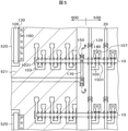
図5はこの問題を対策する本発明を示す平面図である。図5も図1の領域Aに対応する平面図である。図5において、表示領域500には、画素に対応してTFTが縦方向と横方向に所定のピッチで配列している。また、額縁領域600には、周辺回路520が形成され、周辺回路520を覆って、映像信号線20等と同層で形成され、コモン電圧が印加されるコモンバス配線521が形成されていることは図4と同様である。
FIG. 5 is a plan view showing the present invention for solving this problem. FIG. 5 is also a plan view corresponding to region A of FIG. In FIG. 5, in the
図5の特徴は、額縁領域600において、コモンバス配線521の下層に、表示領域600のTFTの構成と類似した、ダミーのTFTが形成されていることである。このダミーのTFTは表示領域500と同じピッチで縦方向と横方向に形成されていることが望ましい。図5では、ダミーのTFTは3列形成されているが、額縁領域600の幅によって数を調整することが出来、最低、1列でも良い。
The feature of FIG. 5 is that a dummy TFT similar to the TFT structure of the
すなわち、静電気によるTFTの破壊は、表示領域500の最外側の画素において生じているので、最外周の画素の外側にダミーのTFTを形成することにより、ダミー画素で静電破壊を生じさせることによって、表示領域500における画素を保護することが出来る。
That is, since the breakdown of the TFT due to static electricity occurs in the outermost pixel of the
なお、図5におけるダミーのTFTを構成する半導体層は、他の導電体とは接続していない。つまり、図5におけるダミーのTFTを構成する半導体層はフロートの状態になっている。なお、図5におけるダミーのTFTを構成する半導体層をフロートにしたくない場合は、スルーホールを介してコモンバス配線521と接続してもよい。
Note that the semiconductor layer constituting the dummy TFT in FIG. 5 is not connected to other conductors. That is, the semiconductor layer constituting the dummy TFT in FIG. 5 is in a float state. If the semiconductor layer constituting the dummy TFT in FIG. 5 is not desired to be floated, it may be connected to the
図5の他の特徴は、走査線10を表示領域500と額縁領域600との境界において、分断し、スルーホール150を介して、映像信号線20と同層で形成された橋絡配線170によって接続していることである。すなわち、静電気によるスパークは、映像信号線20を形成する前に生じている。走査線10は長いので、帯電する電荷量が大きいので、基板を移動した場合の電位の上昇が大きいために、走査線10においてスパークを生ずると考えられる。本発明は、走査線10を分断することにより、走査線10に帯電する電荷量を減少させることによって、静電気による周辺回路の破壊を防止する。
Another feature of FIG. 5 is that the
図6は図5のB−B断面図であり、橋絡配線170部分の断面図である。図6において、走査線10は層間絶縁膜106に形成されたスルーホール150を介して橋絡配線170によって接続されている。したがって、橋絡配線170によって接続されるまでは、走査線10は分断され、分断された走査線10の各々に帯電する電荷量も小さくなるので、基板を製造装置から取り去った時に発生する電位の上昇も抑えることができる。
FIG. 6 is a cross-sectional view taken along the line BB in FIG. 5 and is a cross-sectional view of the bridging
図5において、橋絡配線170は映像信号線20と同じ方向に延在している。橋絡配線170を映像信号線20と同じ方向に延在させることによって、額縁領域600の幅を小さくすることが出来る。図5のように、走査線10を分断しておくことによって、映像信号線20を形成する工程前における走査線10あるいはゲート電極105に起因するスパークを防止することが出来る。映像信号線10を形成した後のスパークの発生頻度は非常に小さいので、本発明の効果は非常に大きい。
In FIG. 5, the bridging
図5において、上側の画素行と下側の画素行とでは、走査線の配線が異なっているが、この実施例では、走査線駆動回路を表示領域の左側と右側に分けて形成しているからである。つまり、図5における下側の走査線は、図1の表示領域の右側に配置した走査線駆動回路から走査信号が供給される。したがって、表示領域の左右において同様な回路配置となっている。 In FIG. 5, the scanning line wiring is different between the upper pixel row and the lower pixel row, but in this embodiment, the scanning line driving circuit is formed separately on the left side and the right side of the display area. Because. That is, the scanning signal is supplied to the lower scanning line in FIG. 5 from the scanning line driving circuit arranged on the right side of the display area in FIG. Therefore, the circuit arrangement is the same on the left and right of the display area.
図5では、映像信号線20が形成された状態までにおける平面図である。その後、映像信号線20の等の上に有機パッシベーション膜108、コモン電極109、容量電極110、画素電極111、配向膜112等が形成される。なお、完成品においては、図5における幅の広いコモンバス配線521の上には、有機パッシベーション膜108を挟んでITOによるコモン電極109が形成されることになる。
FIG. 5 is a plan view up to a state where the
本発明の他の特徴は、スパークが生じて、ダミーTFTが破壊された場合であっても、図7に×で示す、走査線10のB1、B2部分をレーザ等で切断することによって、表示領域の画素に対する影響を無くすことが出来る点である。すなわち、特定走査線における線欠陥不良を防止することが出来、製造歩留まりを向上させることができる。
Another feature of the present invention is that even if a spark is generated and the dummy TFT is destroyed, the B1 and B2 portions of the
以上は、IPS方式の液晶表示装置を例にとって説明したが、本発明は、IPS方式に限らず、他の方式の液晶表示装置についても適用することが出来る。なお、走査線を使用する有機EL表示装置についても適用することが出来る。また、以上の説明では、透明導電膜としてITOを代表として挙げたが、そのほかに、AZO、IZO等も透明導電膜として使用することが出来る。 The above is an example of an IPS liquid crystal display device. However, the present invention is not limited to the IPS method and can be applied to other liquid crystal display devices. Note that the present invention can also be applied to an organic EL display device that uses scanning lines. In the above description, ITO is exemplified as a transparent conductive film, but AZO, IZO, and the like can also be used as the transparent conductive film.
10…走査線10、 20…映像信号線、 50…柱状スペーサ、 100…TFT基板、 101…第1下地膜、 102…第2下地膜、 103…半導体層、 104…ゲート絶縁膜、 105…ゲート電極、 106…層間絶縁膜、 107…コンタクト電極、 108…有機パッシベーション膜、 109…コモン電極、 110…容量絶縁膜、 111…画素電極、 112…配向膜、 115…配向軸、 120…ドレイン側スルーホール、 130…有機パッシベーション膜のスルーホール、 140…ソース側スルーホール、 150…橋絡配線用スルーホール、 160…周辺回路スルーホール、 170…橋絡配線、 200…対向基板、 201…カラーフィルタ、 202…ブラックマトリクス、 203…オーバーコート膜、 300…液晶層、 301…液晶分子、 500…表示領域、 510…端子領域、 520…周辺回路領域、 521…コモンバス配線、 550…シール材、 600…額縁領域、 1031…チャンネル遮光膜、 1111…接続ITO、 D…ドレイン部、S…ソース部
DESCRIPTION OF
Claims (10)
前記基板は、前記走査線に接続された薄膜トランジスタを有する画素がマトリクス状に配列した表示領域と、前記表示領域の外側の周辺領域とを有し、
前記走査線は、前記表示領域と前記周辺領域に延在して形成される第1の走査線と、前記周辺領域において前記第1の走査線と並行して形成される第2の走査線を有し、
前記周辺領域において、前記表示領域との境界に沿って形成される周辺領域配線を有し、
前記周辺領域には、前記周辺領域配線と重畳する位置に複数の半導体層が形成され、
前記第1の走査線は、前記周辺領域において、絶縁膜を介して前記半導体層と重畳しており、
前記第1の走査線と前記第2の走査線は、前記周辺領域配線と前記表示領域間において、橋絡配線によって接続され、
ていることを特徴とする表示装置。 A display device having a substrate in which a plurality of scanning lines extend in a first direction, arranged in a second direction, and a plurality of video signal lines arranged in the first direction,
The substrate has a display region in which pixels having thin film transistors connected to the scanning lines are arranged in a matrix, and a peripheral region outside the display region,
The scanning lines, the display region and the and the first scan line which is formed to extend in the peripheral region, a second scan to be formed in parallel with Oite said first scan line in said peripheral region Have a line,
In the peripheral area, the peripheral area wiring formed along the boundary with the display area,
In the peripheral region, a plurality of semiconductor layers are formed at positions overlapping with the peripheral region wiring,
The first scanning line overlaps with the semiconductor layer via an insulating film in the peripheral region,
The first scanning line and the second scanning line are connected by a bridging wiring between the peripheral region wiring and the display region,
A display device.
前記周辺領域配線は、前記共通電極に印加されるコモン電位が印加されることを特徴とする請求項1乃至3の何れかに記載の表示装置。 The pixel has a pixel electrode and a common electrode,
The display device according to claim 1, wherein a common potential applied to the common electrode is applied to the peripheral region wiring.
前記周辺領域に形成された前記半導体層は、前記映像信号線とは接続していないことを特徴とする請求項1に記載の表示装置。The display device according to claim 1, wherein the semiconductor layer formed in the peripheral region is not connected to the video signal line.
Priority Applications (6)
| Application Number | Priority Date | Filing Date | Title |
|---|---|---|---|
| JP2015189683A JP6621284B2 (en) | 2015-09-28 | 2015-09-28 | Display device |
| US15/237,011 US9678397B2 (en) | 2015-09-28 | 2016-08-15 | Display device |
| US15/605,409 US9983449B2 (en) | 2015-09-28 | 2017-05-25 | Display device |
| US15/968,334 US10228593B2 (en) | 2015-09-28 | 2018-05-01 | Display device |
| US16/252,232 US10488722B2 (en) | 2015-09-28 | 2019-01-18 | Display device |
| US16/583,561 US10768494B2 (en) | 2015-09-28 | 2019-09-26 | Display device |
Applications Claiming Priority (1)
| Application Number | Priority Date | Filing Date | Title |
|---|---|---|---|
| JP2015189683A JP6621284B2 (en) | 2015-09-28 | 2015-09-28 | Display device |
Publications (3)
| Publication Number | Publication Date |
|---|---|
| JP2017067830A JP2017067830A (en) | 2017-04-06 |
| JP2017067830A5 JP2017067830A5 (en) | 2018-10-11 |
| JP6621284B2 true JP6621284B2 (en) | 2019-12-18 |
Family
ID=58407090
Family Applications (1)
| Application Number | Title | Priority Date | Filing Date |
|---|---|---|---|
| JP2015189683A Active JP6621284B2 (en) | 2015-09-28 | 2015-09-28 | Display device |
Country Status (2)
| Country | Link |
|---|---|
| US (5) | US9678397B2 (en) |
| JP (1) | JP6621284B2 (en) |
Families Citing this family (13)
| Publication number | Priority date | Publication date | Assignee | Title |
|---|---|---|---|---|
| JP6621284B2 (en) * | 2015-09-28 | 2019-12-18 | 株式会社ジャパンディスプレイ | Display device |
| CN206074968U (en) * | 2016-10-14 | 2017-04-05 | 京东方科技集团股份有限公司 | Array base palte and display device |
| JP6740108B2 (en) * | 2016-11-30 | 2020-08-12 | 株式会社ジャパンディスプレイ | Display device |
| TWI630445B (en) * | 2017-08-21 | 2018-07-21 | 友達光電股份有限公司 | Active device substrate |
| JP6983006B2 (en) | 2017-08-23 | 2021-12-17 | 株式会社ジャパンディスプレイ | Display device |
| CN107844009B (en) * | 2017-11-22 | 2021-01-29 | Tcl华星光电技术有限公司 | Display device and display panel thereof |
| CN108508642A (en) * | 2018-03-07 | 2018-09-07 | 武汉华星光电技术有限公司 | A kind of liquid crystal display panel and mobile terminal |
| TWI667780B (en) * | 2018-08-02 | 2019-08-01 | 友達光電股份有限公司 | Display panel |
| CN109001950A (en) * | 2018-09-29 | 2018-12-14 | 武汉华星光电技术有限公司 | Array substrate and display device |
| JP7320407B2 (en) * | 2019-08-26 | 2023-08-03 | 株式会社ジャパンディスプレイ | Display device |
| CN113219741B (en) * | 2021-04-20 | 2022-12-13 | 绵阳惠科光电科技有限公司 | Display panel and display device |
| WO2023127161A1 (en) * | 2021-12-29 | 2023-07-06 | シャープディスプレイテクノロジー株式会社 | Display device |
| WO2023127165A1 (en) * | 2021-12-29 | 2023-07-06 | シャープディスプレイテクノロジー株式会社 | Display device |
Family Cites Families (10)
| Publication number | Priority date | Publication date | Assignee | Title |
|---|---|---|---|---|
| JP4777500B2 (en) * | 2000-06-19 | 2011-09-21 | 三菱電機株式会社 | Array substrate, display device using the same, and method of manufacturing array substrate |
| JP2004163493A (en) * | 2002-11-11 | 2004-06-10 | Sanyo Electric Co Ltd | Display device |
| US7119411B2 (en) * | 2004-02-17 | 2006-10-10 | Au Optronics Corp. | Interconnect structure for TFT-array substrate and method for fabricating the same |
| CN1766722A (en) * | 2004-10-28 | 2006-05-03 | 中华映管股份有限公司 | Thin film transistor array substrate, liquid crystal display panel and electrostatic protection method thereof |
| JP2011164329A (en) * | 2010-02-09 | 2011-08-25 | Sony Corp | Electro-optical display panel |
| JP5776305B2 (en) * | 2011-04-25 | 2015-09-09 | セイコーエプソン株式会社 | Electro-optical device and electronic apparatus |
| JP6004560B2 (en) * | 2011-10-06 | 2016-10-12 | 株式会社ジャパンディスプレイ | Display device |
| CN104115060A (en) * | 2012-02-27 | 2014-10-22 | 京瓷株式会社 | Liquid crystal display device |
| JP6320782B2 (en) * | 2014-02-06 | 2018-05-09 | 株式会社ジャパンディスプレイ | Array substrate |
| JP6621284B2 (en) * | 2015-09-28 | 2019-12-18 | 株式会社ジャパンディスプレイ | Display device |
-
2015
- 2015-09-28 JP JP2015189683A patent/JP6621284B2/en active Active
-
2016
- 2016-08-15 US US15/237,011 patent/US9678397B2/en active Active
-
2017
- 2017-05-25 US US15/605,409 patent/US9983449B2/en active Active
-
2018
- 2018-05-01 US US15/968,334 patent/US10228593B2/en active Active
-
2019
- 2019-01-18 US US16/252,232 patent/US10488722B2/en active Active
- 2019-09-26 US US16/583,561 patent/US10768494B2/en active Active
Also Published As
| Publication number | Publication date |
|---|---|
| US20190155114A1 (en) | 2019-05-23 |
| US10228593B2 (en) | 2019-03-12 |
| US20170261822A1 (en) | 2017-09-14 |
| US9983449B2 (en) | 2018-05-29 |
| US20170090256A1 (en) | 2017-03-30 |
| US20200019028A1 (en) | 2020-01-16 |
| US10488722B2 (en) | 2019-11-26 |
| US9678397B2 (en) | 2017-06-13 |
| US10768494B2 (en) | 2020-09-08 |
| US20180246383A1 (en) | 2018-08-30 |
| JP2017067830A (en) | 2017-04-06 |
Similar Documents
| Publication | Publication Date | Title |
|---|---|---|
| JP6621284B2 (en) | Display device | |
| US11506949B2 (en) | Liquid crystal display device | |
| KR102063983B1 (en) | Thin Film Transistor Substrate Having Metal Oxide Semiconductor and Manufacturing Method Thereof | |
| JP2017146450A (en) | Display device | |
| KR101622655B1 (en) | Liquid crystal display device and method of fabricating the same | |
| JP6591194B2 (en) | Liquid crystal display device | |
| TW201508928A (en) | Array substrate of liquid crystal display | |
| JP2017219615A (en) | Liquid crystal display | |
| US9703152B2 (en) | Liquid crystal display device | |
| JP2016015404A (en) | Liquid crystal display device | |
| JP2009069725A (en) | Liquid crystal panel | |
| JP6918090B2 (en) | Liquid crystal display device | |
| JP7201777B2 (en) | liquid crystal display | |
| JP6980730B2 (en) | Liquid crystal display device | |
| KR101969567B1 (en) | Thin Film Transistor Substrate Having Metal Oxide Semiconductor and Manufacturing Method Thereof | |
| US11003031B2 (en) | Display apparatus | |
| KR20170080212A (en) | Display panel and display device having the same | |
| JP2020098356A (en) | TFT substrate | |
| KR20070113812A (en) | Liquid crystal display panel |
Legal Events
| Date | Code | Title | Description |
|---|---|---|---|
| A521 | Request for written amendment filed |
Free format text: JAPANESE INTERMEDIATE CODE: A523 Effective date: 20180824 |
|
| A621 | Written request for application examination |
Free format text: JAPANESE INTERMEDIATE CODE: A621 Effective date: 20180824 |
|
| A977 | Report on retrieval |
Free format text: JAPANESE INTERMEDIATE CODE: A971007 Effective date: 20190627 |
|
| A131 | Notification of reasons for refusal |
Free format text: JAPANESE INTERMEDIATE CODE: A131 Effective date: 20190702 |
|
| A521 | Request for written amendment filed |
Free format text: JAPANESE INTERMEDIATE CODE: A523 Effective date: 20190828 |
|
| TRDD | Decision of grant or rejection written | ||
| A01 | Written decision to grant a patent or to grant a registration (utility model) |
Free format text: JAPANESE INTERMEDIATE CODE: A01 Effective date: 20191105 |
|
| A61 | First payment of annual fees (during grant procedure) |
Free format text: JAPANESE INTERMEDIATE CODE: A61 Effective date: 20191119 |
|
| R150 | Certificate of patent or registration of utility model |
Ref document number: 6621284 Country of ref document: JP Free format text: JAPANESE INTERMEDIATE CODE: R150 |
|
| R250 | Receipt of annual fees |
Free format text: JAPANESE INTERMEDIATE CODE: R250 |
|
| R250 | Receipt of annual fees |
Free format text: JAPANESE INTERMEDIATE CODE: R250 |