JP6602260B2 - Power converter - Google Patents
Power converter Download PDFInfo
- Publication number
- JP6602260B2 JP6602260B2 JP2016101733A JP2016101733A JP6602260B2 JP 6602260 B2 JP6602260 B2 JP 6602260B2 JP 2016101733 A JP2016101733 A JP 2016101733A JP 2016101733 A JP2016101733 A JP 2016101733A JP 6602260 B2 JP6602260 B2 JP 6602260B2
- Authority
- JP
- Japan
- Prior art keywords
- substrate
- switching element
- capacitor
- snubber circuit
- main surface
- Prior art date
- Legal status (The legal status is an assumption and is not a legal conclusion. Google has not performed a legal analysis and makes no representation as to the accuracy of the status listed.)
- Active
Links
Images


Description
本発明は、パワーモジュールを備える電力変換装置に関する。 The present invention relates to a power conversion device including a power module.
電力変換装置は、パワーモジュールを構成するスイッチング素子のスイッチング動作により、入力された直流電力を交流電力に変換、または入力された交流電力を直流電力に変換する。スイッチング素子のスイッチング動作時には電流の急激な変化と主回路配線のインダクタンスとによってサージ電圧が発生し、パワーモジュールが破壊される恐れがある。そこで電力変換装置では、スイッチング素子にコンデンサを並列接続することにより高周波電流を吸収してサージ電圧を低減する方法が採用されている。特許文献1に開示される電力変換装置は、パワーモジュールを搭載した絶縁基板上に、サージ電圧を抑制するためのコンデンサが設けられている。絶縁基板上にコンデンサを設けているのは、コンデンサがスイッチング素子の近くに配置されるほど主回路配線のインダクタンスが低減され、サージ電圧の低減効果が高くなるためである。 The power conversion device converts input DC power into AC power or converts input AC power into DC power by a switching operation of the switching elements constituting the power module. During the switching operation of the switching element, a surge voltage is generated due to a sudden change in current and the inductance of the main circuit wiring, which may destroy the power module. Therefore, in the power converter, a method is adopted in which a surge voltage is reduced by absorbing a high-frequency current by connecting a capacitor in parallel to the switching element. In the power conversion device disclosed in Patent Document 1, a capacitor for suppressing a surge voltage is provided on an insulating substrate on which a power module is mounted. The capacitor is provided on the insulating substrate because the inductance of the main circuit wiring is reduced and the effect of reducing the surge voltage is increased as the capacitor is arranged closer to the switching element.
しかしながら特許文献1に開示される電力変換装置では、パワーモジュールを搭載した絶縁基板上にコンデンサが配置されている。そのためスイッチング素子の動作時に発生した熱が絶縁基板に伝わり、この熱により絶縁基板が膨張してコンデンサに応力が加わるため、コンデンサの故障が生じ易く、コンデンサが溶断して短絡故障した場合、過大な電流によってパワーモジュールが破壊されて電力変換装置の信頼性が損なわれるという課題があった。 However, in the power converter disclosed in Patent Document 1, a capacitor is arranged on an insulating substrate on which a power module is mounted. For this reason, heat generated during the operation of the switching element is transferred to the insulating substrate, which expands the insulating substrate and applies stress to the capacitor. There was a problem that the power module was destroyed by the current and the reliability of the power converter was impaired.
本発明は、上記に鑑みてなされたものであって、信頼性を向上させることができる電力変換装置を得ることを目的とする。 This invention is made | formed in view of the above, Comprising: It aims at obtaining the power converter device which can improve reliability.
上述した課題を解決し、目的を達成するために、本発明の電力変換装置は、第1の主面および第2の主面を有し、スイッチング素子が第1の主面に設置される第1の基板と、第3の主面および第4の主面を有し、スイッチング素子に並列接続されるコンデンサを含むスナバ回路が第3の主面に設置される第2の基板と、スイッチング素子と前記スナバ回路とを電気的に接続する導体とを備え、スイッチング素子が設置された第1の主面が、スナバ回路が設置されている第3の主面と対面しないように、第1の基板と第2の基板が離間して積層される。 In order to solve the above-described problems and achieve the object, the power conversion device of the present invention has a first main surface and a second main surface, and a switching element is installed on the first main surface . A second substrate on which a snubber circuit including a capacitor having one substrate, a third main surface and a fourth main surface and including a capacitor connected in parallel to the switching device is disposed on the third main surface; And a conductor that electrically connects the snubber circuit, and the first main surface on which the switching element is installed does not face the third main surface on which the snubber circuit is installed. The substrate and the second substrate are stacked apart.
本発明の電力変換装置によれば、信頼性を向上させることができるという効果を奏する。 According to the power converter of the present invention, there is an effect that reliability can be improved.
以下に、本発明の実施の形態に係る電力変換装置を図面に基づいて詳細に説明する。なお、この実施の形態によりこの発明が限定されるものではない。 Below, the power converter concerning an embodiment of the invention is explained in detail based on a drawing. Note that the present invention is not limited to the embodiments.
実施の形態1.
図1は実施の形態1に係る電力変換装置の構成例を示す図である。実施の形態1に係る電力変換装置100はパワーモジュール10を備え、パワーモジュール10は、炭化珪素(Silicon Carbide:SiC)を用いて形成された第1のスイッチング素子11aとSiCを用いて形成された第2のスイッチング素子11bとを直列接続したスイッチング素子対11を備える。
Embodiment 1 FIG.
FIG. 1 is a diagram illustrating a configuration example of the power conversion device according to the first embodiment. The
またパワーモジュール10は、スイッチング素子対11に並列接続され、ノイズ除去用のコンデンサ12aを含むスナバ回路12と、溶断部材13とを備える。溶断部材13は、スイッチング素子対11とスナバ回路12とを接続する接続導体に配置され、スナバ回路に一定値以上の電流が流れたときに溶断する。溶断部材13としては、過電流で溶断するヒューズまたはワイヤを例示できる。
Further, the
またパワーモジュール10は、直流電圧源1の正極線1aに接続され、スイッチング素子対11および溶断部材13に第1の電位を与える第1の端子14と、直流電圧源1の負極線1bに接続され、スイッチング素子対11および溶断部材13に第2の電位を与える第2の端子15とを備える。第2の電位は第1の電位よりも低い電位である。またパワーモジュール10は、第1のスイッチング素子11aと第2のスイッチング素子11bとの接続点に接続される第3の端子16を備える。第3の端子16には負荷装置4が接続される。負荷装置4としては回転電機を例示できる。
The
第1の端子14には正極線1a、溶断部材13および第1のスイッチング素子11aが接続される。第2の端子15には負極線1b、スナバ回路12および第2のスイッチング素子11bが接続される。正極線1aと負極線1bとの間には、第1のスイッチング素子11aと第2のスイッチング素子11bとが直列接続され、溶断部材13およびスナバ回路12が直列接続される。図1の例では溶断部材13とスナバ回路12が有するコンデンサ12aとが直列に接続されているが、スナバ回路12はコンデンサ12a以外にも、コンデンサ12aに直列接続されたスナバ抵抗を備える構成でもよい。
The
以下に電力変換装置100の動作を説明する。電力変換装置100が備える駆動制御回路は外部から与えられる電圧指令に基づき第1および第2のスイッチング素子11a,11bを駆動する駆動信号を生成し、生成された駆動信号が第1および第2のスイッチング素子11a,11bに与えられる。第1および第2のスイッチング素子11a,11bではスイッチング動作が行われることにより、一定の電圧および周波数の擬似正弦波が負荷装置4に供給される。第1および第2のスイッチング素子11a,11bのスイッチング動作時の電流の急激な変化と主回路配線のインダクタンスとによって生じるサージ電圧は、スナバ回路12により低減される。
The operation of the
本実施の形態に係るパワーモジュール10では、第1および第2のスイッチング素子11a,11bが設置される第1の基板と、スナバ回路12を構成するコンデンサ12aが設置される第2の基板とを備え、当該第1および第2の基板が、溶断部材13を含む接続導体により相互に接続されている点に特徴がある。
In the
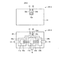
図2は図1に示す第1および第2のスイッチング素子が設置される第1の基板と、図1に示すコンデンサが設置される第2の基板との斜視図である。図2では、パワーモジュール10が有する第1の基板20および第2の基板30のそれぞれの端面22および端面32が対向するように配置されている。第1の基板20は、金属ベース板20A上に設けられた絶縁層25と、第1および第2のスイッチング素子11a,11bとを備える。第1および第2のスイッチング素子11a,11bは第1の基板20の基板面21に設けられている。第2の基板30の基板面31にはコンデンサ12aが設けられている。
FIG. 2 is a perspective view of the first substrate on which the first and second switching elements shown in FIG. 1 are installed and the second substrate on which the capacitor shown in FIG. 1 is installed. In FIG. 2, the
第1の基板20および第2の基板30は、第1の接続導体41および第2の接続導体42により相互に接続される。第1の接続導体41は、第1のスイッチング素子11aとコンデンサ12aとを電気的に接続するための接続導体である。第2の接続導体42は、第2のスイッチング素子11bとコンデンサ12aとを電気的に接続するための接続導体である。このようにパワーモジュール10は、第1の基板20、第2の基板30、第1の接続導体41および第2の接続導体42を備える。
The
図3は図2に示す第1の基板および第2の基板を上面側から見た平面図である。絶縁基板である第1の基板20は、金属ベース板20A上に設けられた絶縁層25と、P側導体パターン23aと、N側導体パターン23bと、出力導体パターン23cとを備える。P側導体パターン23aの上面には第1のスイッチング素子11aおよび第1の端子14が配置されている。N側導体パターン23bの上面には第2の端子15が配置されている。出力導体パターン23cの上面には、第2のスイッチング素子11bおよび第3の端子16が配置されている。
FIG. 3 is a plan view of the first substrate and the second substrate shown in FIG. 2 as viewed from the upper surface side. The
P側導体パターン23aには、第1の端子14、第1のスイッチング素子11aおよび第1の接続導体41が接続される。第1のスイッチング素子11aおよび出力導体パターン23cは、導電性のワイヤ24aにより相互に接続される。出力導体パターン23cには、第2のスイッチング素子11b、第3の端子16およびワイヤ24bが接続される。N側導体パターン23bにはワイヤ24b、第2の端子15および第2の接続導体42が接続される。
The
制御基板である第2の基板30は、プリント基板で構成されており、コンデンサ12a、P側導体パターン32aおよびN側導体パターン32bを備える。
The
コンデンサ12aの一端はP側導体パターン32aに接続される。P側導体パターン32aには第1の接続導体41が接続される。P側導体パターン32aおよびP側導体パターン23aは第1の接続導体41を介して相互に接続されている。コンデンサ12aの他端はN側導体パターン32bに接続される。N側導体パターン32bには第2の接続導体42が接続される。N側導体パターン32bおよびN側導体パターン23bは第2の接続導体42を介して相互に接続されている。
One end of the
絶縁層25、P側導体パターン23a、N側導体パターン23b、ワイヤ24a、ワイヤ24b、第1のスイッチング素子11a、第2のスイッチング素子11b、第1の接続導体41、第2の接続導体42、コンデンサ12aおよび基板面31は、ケース50の内部に配置されている。ケース50内部には樹脂51が封入されている。金属ベース板20Aの端部はケース50の外部に露出しており、第1の基板20の底面を構成している。
Insulating
第1の端子14はP側導体パターン23aとの接続端の反対側がケース50の外部に露出している。同様に、第2の端子15はN側導体パターン23bとの接続端の反対側がケース50の外部に露出している。第3の端子16は出力導体パターン23cとの接続端の反対側がケース50の外部に露出している。
The
溶断部材13はコンデンサ12aが短絡故障したときに溶断するように断面積が設定されている。なお図3では第1の接続導体41に溶断部材13が設けられているが、溶断部材13の位置は図示例に限定されず、第1のスイッチング素子11aとコンデンサ12aとの間の導体内に配置されていればよい。すなわち溶断部材13は、溶断部材13は第1の接続導体41および第2の接続導体42の少なくとも一方に設けられていればよい。また溶断部材13は、P側導体パターン23aおよびN側導体パターン23bの何れかに設けてもよいし、P側導体パターン32aおよびN側導体パターン32bの何れかに設けてもよい。
The fusing
本実施の形態におけるパワーモジュール10では樹脂51が封入された第2の基板30の熱膨張係数が、金属ベース板20Aを含む第1の基板20の熱膨張係数よりも小さい。このように実施の形態1に係る電力変換装置100は、スイッチング素子対11が設置される第1の基板20と、スイッチング素子対11に並列接続されるスナバ回路12が設置される第2の基板30と、スイッチング素子対11とスナバ回路12とを接続する導体である第1および第2の接続導体41,42とを備え、第2の基板30の熱膨張係数は第1の基板20の熱膨張係数よりも小さく構成されている。
In the
スイッチング素子対11の動作時に発生した熱は、主に金属ベース板20Aに伝わり、金属ベース板20Aから放熱されるが、熱の一部は樹脂51、P側導体パターン23a、N側導体パターン23bおよび絶縁層25にも伝わる。前述した特許文献1に示す従来技術では、スイッチング素子の動作時に発生した熱が絶縁基板に伝わり、この熱により絶縁基板が膨張し、絶縁基板と同一の基板面に設置されたコンデンサに応力が加わるため、この応力に起因したコンデンサの短絡故障が生じ易いという問題点があった。これに対して実施の形態1に係る電力変換装置100は、コンデンサ12aを含むスナバ回路12が、スイッチング素子対11の設置される第1の基板20とは別の第2の基板30に設置されている。従って特許文献1に示す従来技術に比べて、スイッチング素子対11の動作時に発生した熱が第2の基板30に伝わり難く、第2の基板30からコンデンサ12aに加えられる応力が小さい。従って第2の基板30からの応力に起因したコンデンサ12aの短絡故障が抑制される。
The heat generated during the operation of the switching element pair 11 is mainly transmitted to the
さらに実施の形態1に係る電力変換装置100では、第2の基板30の熱膨張係数が第1の基板20の熱膨張係数よりも小さく構成されている。従ってスイッチング素子対11の動作時に発生した熱の一部が樹脂51、P側導体パターン23aおよびN側導体パターン23bを介して第2の基板30に伝わった場合でも、第1の基板20にコンデンサ12aが設置されている場合に作用する応力よりも小さい応力が第2の基板30上のコンデンサ12aに作用する。そのため、第2の基板30からの応力に起因したコンデンサ12aの短絡故障がより一層抑制される。
Furthermore, in the
上記の熱膨張係数の違いによる効果を実現するため、例えば、第1の基板20は金属ベース板20Aを有するが、第2の基板30は、金属ベース板に代わって樹脂板を有していてもよい。なお、第2の基板30が第1の基板20よりも熱膨張係数の小さい金属ベース板を用いてもよいことは言うまでもない。
In order to realize the effect due to the difference in the thermal expansion coefficient, for example, the
また実施の形態1に係る電力変換装置100では、スナバ回路12に一定値以上の電流が流れたときに溶断する溶断部材13が、スイッチング素子対11とスナバ回路12とを接続する導体内に配置されている。そのため、コンデンサ12aが短絡故障した場合でも電流によって発生する熱で溶断部材13が溶断されるため、過大な電流によってパワーモジュール10の周囲の装置である負荷装置4が故障するというような2次被害の発生を抑制できる。
In the
また実施の形態1に係る電力変換装置100では、パワーモジュール10にコンデンサ12aが内蔵されているため、パワーモジュール10の外部にコンデンサ12aを配置する場合に比べて、コンデンサ12aからスイッチング素子対11までの配線によるインダクタンスを低減でき、インダクタンスに起因するサージ電圧を低減できる。
In the
また実施の形態1に係る電力変換装置100では、第2の基板30の基板面31の内、第1の基板20と第2の基板30との対向面の近くにコンデンサ12aを配置することにより、コンデンサ12aから第1および第2のスイッチング素子11a,11bまでの配線長、特に第1および第2の接続導体41,42の長さを短くしている。例えば、第2の基板30の基板面31における中心点よりも第1の基板20側にコンデンサ12aを配置すれば良い。すなわち実施の形態1に係る電力変換装置100では、スイッチング素子対11の近くにコンデンサ12aが配置されている。これにより、コンデンサ12aからスイッチング素子対11までの配線によるインダクタンスをより一層低減でき、インダクタンスに起因するサージ電圧をより一層低減できる。
In the
実施の形態2.
図4は実施の形態2に係る電力変換装置が備えるパワーモジュールの第1の基板および第2の基板を示す図である。図5は図4に示す第1の基板および第2の基板をそれぞれの基板面が対向するように配置された状態を示す図である。実施の形態1と実施の形態2の相違点は以下の通りである。
(1)実施の形態2のパワーモジュール10−2は、実施の形態1の第1の基板20および第2の基板30の代わりに第1の基板20−2および第2の基板30−2を備えること。
(2)第1の基板20−2は、実施の形態1の第1の基板20に設けられる構成に加えて、N側導体パターン23dおよびワイヤ24cを備えること。
(3)第1の基板20−2は、第2の基板30−2と同一平面上に配置されていないこと。すなわち、第1の基板20−2は第2の基板30−2と一定距離、離間して重なるように配置されること。
(4)第2の基板30−2は、第1の基板20−2との対向面とは反対側の基板面31、すなわち図4における上面側に、P側導体パターン32a、N側導体パターン32bおよびコンデンサ12aが設けられていること。
(5)第1の接続導体41とP側導体パターン32aは、第1の基板20−2の上面である基板面21と第2の基板30−2の裏面が対向した状態で、第1および第2の接続導体41,42が設けられていること。第2の基板30−2の裏面とは、基板面31とは反対側の面である。
Embodiment 2. FIG.
FIG. 4 is a diagram illustrating a first substrate and a second substrate of a power module included in the power conversion device according to the second embodiment. FIG. 5 is a diagram showing a state in which the first substrate and the second substrate shown in FIG. 4 are arranged so that their substrate surfaces face each other. Differences between the first embodiment and the second embodiment are as follows.
(1) The power module 10-2 according to the second embodiment includes the first substrate 20-2 and the second substrate 30-2 instead of the
(2) In addition to the structure provided in the 1st board |
(3) The first substrate 20-2 is not disposed on the same plane as the second substrate 30-2. That is, the first substrate 20-2 is disposed so as to be separated from the second substrate 30-2 by a predetermined distance.
(4) The second substrate 30-2 has a P-
(5) The
図4および図5では、図2および図3に示す金属ベース板20A、ケース50および樹脂51の図示を省略しているが、絶縁層25、P側導体パターン23a、N側導体パターン23b、ワイヤ24a、ワイヤ24b、第1のスイッチング素子11a、第2のスイッチング素子11b、第1の接続導体41、第2の接続導体42、コンデンサ12a、基板面31、N側導体パターン23dおよびワイヤ24cは、ケース50の内部に配置されている。またケース50内部には樹脂51が封入されている。金属ベース板20Aの端部はケース50の外部に露出しており、第1の基板20−2の底面を構成している。
4 and 5, illustration of the
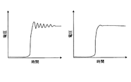
図6はSiCで形成された第1および第2のスイッチング素子を内蔵するパワーモジュールで発生する電圧振動を説明するための図である。左側の図は実施の形態1,2に係るコンデンサ12aを第1および第2のスイッチング素子11a,11bから遠ざけた位置に配置した場合の図である。右側の図は実施の形態1,2に係るコンデンサ12aを図3および図5に示す位置に配置した場合の図である。縦軸は電圧振動を表し、横軸は時間を表す。
FIG. 6 is a diagram for explaining voltage oscillation generated in a power module including the first and second switching elements formed of SiC. The figure on the left is a diagram in the case where the
遠ざけた位置とは、図3に示すパワーモジュール10では、第2の基板30の基板面31の内、第1の基板20と第2の基板30との対向面の反対側、すなわち図3の紙面上側にコンデンサ12aが配置されていることを例示できる。例えば、第2の基板30の中心点よりも第1の基板20と反対側にコンデンサ12aが配置されている場合があげられる。また遠ざけた位置とは、図5に示すパワーモジュール10−2では、第1の基板20−2と第2の基板30−2との離間距離を大きくすることで相対的に第1および第2のスイッチング素子11a,11bからコンデンサ12aまでの距離を大きくすることを例示できる。
In the
なお実施の形態1,2ではSiCで形成された第1および第2のスイッチング素子11a,11bが用いられているが、SiCで形成された第1および第2のスイッチング素子11a,11bは、低損失な反面、リンギングという電圧振動が大きいことが知られている。それに伴いSiCで形成されたスイッチング素子を用いた電力変換装置では、配線パターンのインダクタンスに起因したリンギングによるノイズの増大が懸念される。
In the first and second embodiments, the first and
この対策として、実施の形態1のパワーモジュール10は、第2の基板30の基板面31の内、第1の基板20と第2の基板30との対向面の近くにコンデンサ12aを配置することにより、コンデンサ12aから第1および第2のスイッチング素子11a,11bまでの配線長、特に第1および第2の接続導体41,42の長さを短くしている。また実施の形態2のパワーモジュール10−2は、第1および第2の基板30−1,30−2のそれぞれの基板面21,31が対向した状態で第1および第2の接続導体41,42が設けられているため、第1および第2の接続導体41,42の長さを短くできる。第1および第2の接続導体41,42を短くすることにより図6に示すように電圧振動が低減してノイズが軽減される。そのため実施の形態1,2に係る電力変換装置は、SiCの低損失性を発揮しながら信頼性を確保できる。
As a countermeasure against this, in the
本実施の形態に係るパワーモジュール10−2は、第1の基板20−2と第2の基板30−2が積層方向(上下方向)に順に配置されている。ここで、コンデンサ12aは、図5に示すように第2の基板30−2の上面側に設けられていてもよいが、第2の基板30−2の裏面側に設けられていてもよい。第2の基板30−2の裏面、すなわち第1の基板20−1と対向する面にコンデンサ12aを設けた場合、第1および第2の接続導体41,42の長さをより短くできる効果が得られ、信頼性の高い電力変換装置が得られる。
In the power module 10-2 according to the present embodiment, the first substrate 20-2 and the second substrate 30-2 are sequentially arranged in the stacking direction (vertical direction). Here, the
また、図5では第1の基板20−2の上面側に第2の基板30−2を設けたが、積層順を逆にしてもよいことは言うまでもない。ただし、発熱性の高い第1の基板20−2を放熱用部品の設置側に設けることが望ましい。 In FIG. 5, the second substrate 30-2 is provided on the upper surface side of the first substrate 20-2, but it goes without saying that the stacking order may be reversed. However, it is desirable to provide the first substrate 20-2 having high heat generation on the installation side of the heat dissipation component.
なお実施の形態1,2に係る第1および第2のスイッチング素子11a,11bはSic以外のワイドギャップ半導体を用いて構成して同様の効果を得ることができる。ワイドギャップ半導体としてはSiC以外にも窒化ガリウムを例示できる。
The first and
また実施の形態1,2に係る溶断部材はワイヤで構成してもよい。これによりヒューズを例示を用いる場合に比べて溶断部材を安価に製造可能である。 Further, the fusing member according to the first and second embodiments may be formed of a wire. Accordingly, the fusing member can be manufactured at a lower cost than the case where the fuse is used as an example.
また実施の形態1,2に係るスナバ回路は、コンデンサと抵抗を備える構成でもよい。これによりコンデンサのみの場合に比べてサージ電圧をより一層抑制できる。 Further, the snubber circuit according to the first and second embodiments may be configured to include a capacitor and a resistor. Thereby, the surge voltage can be further suppressed as compared with the case of using only the capacitor.
また実施の形態1,2に係る電力変換装置100は、コンデンサまたは抵抗の電極の一端がワイヤに接続され、コンデンサまたは抵抗の電極の他端が第2の基板の導体パターンに接続されている構成でもよい。例えば、コンデンサの電極の一つが表面側に形成されており、当該表面側の電極が接続導体であるワイヤに接続されていてもよい。これによりコンデンサまたは抵抗の電極が直接ワイヤと接続されるため、ワイヤと導体パターンとの接続箇所を減らすことができる。その結果、コンデンサまたは抵抗の実装面積を小さくできる。
In addition,
なお第1の基板と第2の基板のそれぞれの構成は、本実施の形態に限定されず、また本実施の形態では、第1の基板と第2の基板を含むパワーモジュールについて記載したが、第1の基板以外の場所に設置されたパワーモジュールと第2の基板との組み合わせるほか、種々の実施の形態も可能である。 In addition, although each structure of the 1st board | substrate and the 2nd board | substrate is not limited to this Embodiment, In this Embodiment, although the power module containing a 1st board | substrate and a 2nd board | substrate was described, In addition to the combination of the power module installed in a place other than the first substrate and the second substrate, various embodiments are possible.
以上の実施の形態に示した構成は、本発明の内容の一例を示すものであり、別の公知の技術と組み合わせることも可能であるし、本発明の要旨を逸脱しない範囲で、構成の一部を省略、変更することも可能である。 The configuration described in the above embodiment shows an example of the content of the present invention, and can be combined with another known technique, and can be combined with other configurations within the scope of the present invention. It is also possible to omit or change the part.
1 直流電圧源、1a 正極線、1b 負極線、4 負荷装置、10,10−2 パワーモジュール、11 スイッチング素子対、11a 第1のスイッチング素子、11b 第2のスイッチング素子、12 スナバ回路、12a コンデンサ、13 溶断部材、14 第1の端子、15 第2の端子、16 第3の端子、20,20−2 第1の基板、20A 金属ベース板、21 基板面、22 端面、23a,32a P側導体パターン、23b,32b N側導体パターン、23c 出力導体パターン、23d N側導体パターン、24a,24b,24c ワイヤ、25 絶縁層、30,30−2 第2の基板、31 基板面、32 端面、41 第1の接続導体、42 第2の接続導体、50 ケース、100 電力変換装置。 DESCRIPTION OF SYMBOLS 1 DC voltage source, 1a positive electrode line, 1b negative electrode line, 4 load apparatus, 10, 10-2 power module, 11 switching element pair, 11a 1st switching element, 11b 2nd switching element, 12 snubber circuit, 12a capacitor , 13 Fusing member, 14 First terminal, 15 Second terminal, 16 Third terminal, 20, 20-2 First substrate, 20A Metal base plate, 21 Substrate surface, 22 End surface, 23a, 32a P side Conductor pattern, 23b, 32b N side conductor pattern, 23c Output conductor pattern, 23d N side conductor pattern, 24a, 24b, 24c wire, 25 insulation layer, 30, 30-2 Second substrate, 31 substrate surface, 32 end surface, 41 1st connection conductor, 42 2nd connection conductor, 50 cases, 100 power converter.
Claims (10)
第3の主面および第4の主面を有し、前記スイッチング素子に並列接続されるコンデンサを含むスナバ回路が前記第3の主面に設置される第2の基板と、
前記スイッチング素子と前記スナバ回路とを電気的に接続する導体と、
を備え、
前記スイッチング素子が設置された前記第1の主面が、前記スナバ回路が設置されている前記第3の主面と対面しないように、前記第1の基板と前記第2の基板が離間して積層されることを特徴とする電力変換装置。 A first substrate having a first main surface and a second main surface, the switching element being installed on the first main surface ;
A second substrate on which a snubber circuit having a third main surface and a fourth main surface and including a capacitor connected in parallel to the switching element is disposed on the third main surface ;
A conductor that electrically connects the switching element and the snubber circuit ;
Equipped with a,
The first substrate and the second substrate are separated so that the first main surface on which the switching element is installed does not face the third main surface on which the snubber circuit is installed. A power converter characterized by being stacked .
を特徴とする請求項1に記載の電力変換装置。 The power converter according to claim 1, wherein the second substrate has a smaller thermal expansion coefficient than the first substrate.
前記コンデンサの電極の他端は前記第2の基板の導体パターンに接続されていることを特徴とする請求項5に記載の電力変換装置。 One end of the capacitor electrode is connected to the wire;
The power converter according to claim 5 , wherein the other end of the capacitor electrode is connected to a conductor pattern of the second substrate.
前記抵抗、前記コンデンサおよび前記ワイヤは直列に接続されていることを特徴とする請求項5に記載の電力変換装置。 The snubber circuit comprises a resistor,
The power converter according to claim 5 , wherein the resistor, the capacitor, and the wire are connected in series.
前記スイッチング素子に並列接続されるコンデンサを含むスナバ回路が設置される第2の基板と、A second substrate on which a snubber circuit including a capacitor connected in parallel to the switching element is installed;
前記スイッチング素子と前記スナバ回路とを電気的に接続する導体と、A conductor that electrically connects the switching element and the snubber circuit;
前記導体に配置され、前記スナバ回路に一定値以上の電流が流れたときに溶断するワイヤと、A wire disposed on the conductor and fusing when a current of a certain value or more flows through the snubber circuit;
を備えることを特徴とする電力変換装置。A power conversion device comprising:
Priority Applications (1)
| Application Number | Priority Date | Filing Date | Title |
|---|---|---|---|
| JP2016101733A JP6602260B2 (en) | 2016-05-20 | 2016-05-20 | Power converter |
Applications Claiming Priority (1)
| Application Number | Priority Date | Filing Date | Title |
|---|---|---|---|
| JP2016101733A JP6602260B2 (en) | 2016-05-20 | 2016-05-20 | Power converter |
Publications (3)
| Publication Number | Publication Date |
|---|---|
| JP2017208987A JP2017208987A (en) | 2017-11-24 |
| JP2017208987A5 JP2017208987A5 (en) | 2018-10-11 |
| JP6602260B2 true JP6602260B2 (en) | 2019-11-06 |
Family
ID=60416608
Family Applications (1)
| Application Number | Title | Priority Date | Filing Date |
|---|---|---|---|
| JP2016101733A Active JP6602260B2 (en) | 2016-05-20 | 2016-05-20 | Power converter |
Country Status (1)
| Country | Link |
|---|---|
| JP (1) | JP6602260B2 (en) |
Families Citing this family (6)
| Publication number | Priority date | Publication date | Assignee | Title |
|---|---|---|---|---|
| JP2019186983A (en) * | 2018-04-02 | 2019-10-24 | 株式会社豊田中央研究所 | Snubber capacitor incorporated semiconductor power module |
| JP6844746B2 (en) * | 2018-04-19 | 2021-03-17 | 三菱電機株式会社 | Power converter |
| JP7006547B2 (en) * | 2018-09-10 | 2022-01-24 | 三菱電機株式会社 | Semiconductor device |
| JP7038632B2 (en) | 2018-09-12 | 2022-03-18 | 三菱電機株式会社 | Semiconductor devices and methods for manufacturing semiconductor devices |
| JP7142784B2 (en) * | 2019-07-24 | 2022-09-27 | 日立Astemo株式会社 | electric circuit device |
| JP7358921B2 (en) | 2019-11-08 | 2023-10-11 | 富士電機株式会社 | Semiconductor module and semiconductor module manufacturing method |
Family Cites Families (3)
| Publication number | Priority date | Publication date | Assignee | Title |
|---|---|---|---|---|
| JP4901652B2 (en) * | 2007-08-31 | 2012-03-21 | 三菱電機株式会社 | Semiconductor device assembly method and semiconductor device |
| JP5258721B2 (en) * | 2009-09-18 | 2013-08-07 | 三菱電機株式会社 | Inverter device |
| JP5860784B2 (en) * | 2012-09-10 | 2016-02-16 | 日立オートモティブシステムズ株式会社 | Power semiconductor module |
-
2016
- 2016-05-20 JP JP2016101733A patent/JP6602260B2/en active Active
Also Published As
| Publication number | Publication date |
|---|---|
| JP2017208987A (en) | 2017-11-24 |
Similar Documents
| Publication | Publication Date | Title |
|---|---|---|
| JP6602260B2 (en) | Power converter | |
| US10153708B2 (en) | Three-level power converter | |
| JP5169353B2 (en) | Power module | |
| JP5351107B2 (en) | Capacitor cooling structure and inverter device | |
| US10134718B2 (en) | Power semiconductor module | |
| JP7457812B2 (en) | Semiconductor Module | |
| JP4640213B2 (en) | Power semiconductor device and inverter bridge module using the same | |
| JPWO2015121899A1 (en) | Power semiconductor module | |
| JP2002373971A (en) | Semiconductor device | |
| JP2013219290A (en) | Semiconductor device | |
| JP2009027778A (en) | Bus bar | |
| JP6331294B2 (en) | Semiconductor device | |
| JP2007173703A (en) | Semiconductor device | |
| WO2016047174A1 (en) | Power conversion device | |
| JP2007329387A (en) | Semiconductor device | |
| JP2007325387A (en) | Power conversion device | |
| JP2011130626A (en) | Module for semiconductor switch | |
| WO2017179264A1 (en) | Heat dissipation structure of semiconductor device | |
| JPWO2016071982A1 (en) | Semiconductor module and conductive member for semiconductor module | |
| JP6394459B2 (en) | Semiconductor device | |
| JP6766965B2 (en) | Power converter | |
| JP2005191233A (en) | Power module | |
| JP2015018856A (en) | Semiconductor power module | |
| JP6584333B2 (en) | Power module | |
| JP7294289B2 (en) | power converter |
Legal Events
| Date | Code | Title | Description |
|---|---|---|---|
| A521 | Request for written amendment filed |
Free format text: JAPANESE INTERMEDIATE CODE: A523 Effective date: 20180831 |
|
| A621 | Written request for application examination |
Free format text: JAPANESE INTERMEDIATE CODE: A621 Effective date: 20180831 |
|
| A131 | Notification of reasons for refusal |
Free format text: JAPANESE INTERMEDIATE CODE: A131 Effective date: 20190618 |
|
| A977 | Report on retrieval |
Free format text: JAPANESE INTERMEDIATE CODE: A971007 Effective date: 20190619 |
|
| A521 | Request for written amendment filed |
Free format text: JAPANESE INTERMEDIATE CODE: A523 Effective date: 20190805 |
|
| TRDD | Decision of grant or rejection written | ||
| A01 | Written decision to grant a patent or to grant a registration (utility model) |
Free format text: JAPANESE INTERMEDIATE CODE: A01 Effective date: 20190910 |
|
| A61 | First payment of annual fees (during grant procedure) |
Free format text: JAPANESE INTERMEDIATE CODE: A61 Effective date: 20191008 |
|
| R150 | Certificate of patent or registration of utility model |
Ref document number: 6602260 Country of ref document: JP Free format text: JAPANESE INTERMEDIATE CODE: R150 |
|
| R250 | Receipt of annual fees |
Free format text: JAPANESE INTERMEDIATE CODE: R250 |
|
| R250 | Receipt of annual fees |
Free format text: JAPANESE INTERMEDIATE CODE: R250 |