JP6579201B2 - Inductor component and method of manufacturing inductor component - Google Patents
Inductor component and method of manufacturing inductor component Download PDFInfo
- Publication number
- JP6579201B2 JP6579201B2 JP2017560393A JP2017560393A JP6579201B2 JP 6579201 B2 JP6579201 B2 JP 6579201B2 JP 2017560393 A JP2017560393 A JP 2017560393A JP 2017560393 A JP2017560393 A JP 2017560393A JP 6579201 B2 JP6579201 B2 JP 6579201B2
- Authority
- JP
- Japan
- Prior art keywords
- metal
- resin layer
- metal pin
- inductor
- metal plate
- Prior art date
- Legal status (The legal status is an assumption and is not a legal conclusion. Google has not performed a legal analysis and makes no representation as to the accuracy of the status listed.)
- Active
Links
- 238000004519 manufacturing process Methods 0.000 title description 23
- 229910052751 metal Inorganic materials 0.000 claims description 213
- 239000002184 metal Substances 0.000 claims description 213
- 229920005989 resin Polymers 0.000 claims description 107
- 239000011347 resin Substances 0.000 claims description 107
- 230000002093 peripheral effect Effects 0.000 claims description 24
- 238000005304 joining Methods 0.000 claims description 20
- 229910000679 solder Inorganic materials 0.000 claims description 13
- 230000001678 irradiating effect Effects 0.000 claims description 3
- 239000010410 layer Substances 0.000 description 73
- 238000007747 plating Methods 0.000 description 10
- 238000000034 method Methods 0.000 description 9
- 239000004020 conductor Substances 0.000 description 7
- 238000012986 modification Methods 0.000 description 5
- 230000004048 modification Effects 0.000 description 5
- 229920001187 thermosetting polymer Polymers 0.000 description 5
- 239000003822 epoxy resin Substances 0.000 description 4
- 239000000463 material Substances 0.000 description 4
- 229920000647 polyepoxide Polymers 0.000 description 4
- 230000001681 protective effect Effects 0.000 description 4
- 239000012212 insulator Substances 0.000 description 3
- 239000012762 magnetic filler Substances 0.000 description 3
- 238000005498 polishing Methods 0.000 description 3
- 239000012790 adhesive layer Substances 0.000 description 2
- 229910045601 alloy Inorganic materials 0.000 description 2
- 239000000956 alloy Substances 0.000 description 2
- 239000007769 metal material Substances 0.000 description 2
- 239000000843 powder Substances 0.000 description 2
- 238000003892 spreading Methods 0.000 description 2
- 239000000126 substance Substances 0.000 description 2
- 229910000881 Cu alloy Inorganic materials 0.000 description 1
- 229910002482 Cu–Ni Inorganic materials 0.000 description 1
- 229910017827 Cu—Fe Inorganic materials 0.000 description 1
- 239000004642 Polyimide Substances 0.000 description 1
- 230000005540 biological transmission Effects 0.000 description 1
- 229910052802 copper Inorganic materials 0.000 description 1
- 238000010586 diagram Methods 0.000 description 1
- 238000007598 dipping method Methods 0.000 description 1
- 230000000694 effects Effects 0.000 description 1
- 238000005530 etching Methods 0.000 description 1
- 230000020169 heat generation Effects 0.000 description 1
- 239000011229 interlayer Substances 0.000 description 1
- 150000002739 metals Chemical class 0.000 description 1
- 238000000059 patterning Methods 0.000 description 1
- 229920001721 polyimide Polymers 0.000 description 1
- 238000010008 shearing Methods 0.000 description 1
- 229910052709 silver Inorganic materials 0.000 description 1
- 239000000758 substrate Substances 0.000 description 1
- 238000004804 winding Methods 0.000 description 1
- 229910000859 α-Fe Inorganic materials 0.000 description 1
Images


Classifications
-
- H—ELECTRICITY
- H01—ELECTRIC ELEMENTS
- H01F—MAGNETS; INDUCTANCES; TRANSFORMERS; SELECTION OF MATERIALS FOR THEIR MAGNETIC PROPERTIES
- H01F17/00—Fixed inductances of the signal type
- H01F17/0006—Printed inductances
- H01F17/0013—Printed inductances with stacked layers
-
- H—ELECTRICITY
- H01—ELECTRIC ELEMENTS
- H01F—MAGNETS; INDUCTANCES; TRANSFORMERS; SELECTION OF MATERIALS FOR THEIR MAGNETIC PROPERTIES
- H01F27/00—Details of transformers or inductances, in general
- H01F27/28—Coils; Windings; Conductive connections
- H01F27/29—Terminals; Tapping arrangements for signal inductances
-
- H—ELECTRICITY
- H01—ELECTRIC ELEMENTS
- H01F—MAGNETS; INDUCTANCES; TRANSFORMERS; SELECTION OF MATERIALS FOR THEIR MAGNETIC PROPERTIES
- H01F17/00—Fixed inductances of the signal type
- H01F17/0006—Printed inductances
- H01F17/0033—Printed inductances with the coil helically wound around a magnetic core
-
- H—ELECTRICITY
- H01—ELECTRIC ELEMENTS
- H01F—MAGNETS; INDUCTANCES; TRANSFORMERS; SELECTION OF MATERIALS FOR THEIR MAGNETIC PROPERTIES
- H01F17/00—Fixed inductances of the signal type
- H01F17/04—Fixed inductances of the signal type with magnetic core
- H01F17/06—Fixed inductances of the signal type with magnetic core with core substantially closed in itself, e.g. toroid
- H01F17/062—Toroidal core with turns of coil around it
-
- H—ELECTRICITY
- H01—ELECTRIC ELEMENTS
- H01F—MAGNETS; INDUCTANCES; TRANSFORMERS; SELECTION OF MATERIALS FOR THEIR MAGNETIC PROPERTIES
- H01F27/00—Details of transformers or inductances, in general
- H01F27/28—Coils; Windings; Conductive connections
- H01F27/32—Insulating of coils, windings, or parts thereof
- H01F27/324—Insulation between coil and core, between different winding sections, around the coil; Other insulation structures
-
- H—ELECTRICITY
- H01—ELECTRIC ELEMENTS
- H01F—MAGNETS; INDUCTANCES; TRANSFORMERS; SELECTION OF MATERIALS FOR THEIR MAGNETIC PROPERTIES
- H01F41/00—Apparatus or processes specially adapted for manufacturing or assembling magnets, inductances or transformers; Apparatus or processes specially adapted for manufacturing materials characterised by their magnetic properties
- H01F41/02—Apparatus or processes specially adapted for manufacturing or assembling magnets, inductances or transformers; Apparatus or processes specially adapted for manufacturing materials characterised by their magnetic properties for manufacturing cores, coils, or magnets
- H01F41/04—Apparatus or processes specially adapted for manufacturing or assembling magnets, inductances or transformers; Apparatus or processes specially adapted for manufacturing materials characterised by their magnetic properties for manufacturing cores, coils, or magnets for manufacturing coils
- H01F41/041—Printed circuit coils
-
- H—ELECTRICITY
- H01—ELECTRIC ELEMENTS
- H01F—MAGNETS; INDUCTANCES; TRANSFORMERS; SELECTION OF MATERIALS FOR THEIR MAGNETIC PROPERTIES
- H01F17/00—Fixed inductances of the signal type
- H01F17/0006—Printed inductances
- H01F17/0013—Printed inductances with stacked layers
- H01F2017/002—Details of via holes for interconnecting the layers
Description
本発明は、絶縁体に設けられたインダクタを備えるインダクタ部品とその製造方法に関する。 The present invention relates to an inductor component including an inductor provided on an insulator and a method for manufacturing the same.
従来、樹脂層などの絶縁体にインダクタ電極が設けられたインダクタ部品が知られている。この種のインダクタ部品に設けられるインダクタ電極の中には、樹脂層に形成されたビア導体と樹脂層の主面に形成された配線パターンで形成されるものがある。この場合、ビア導体や配線パターンは、導電性ペーストやめっきで形成されるのが一般的である。発明者は、インダクタ電極の特性(例えば、インダクタンス値)の向上や製造コストの低減を図るために、ビア導体に代えて金属ピンを使用するとともに、配線パターンに代えて配線用の金属板を使用してインダクタ電極を形成することを検討している。この構成によると、インダクタ電極全体の低抵抗化を図ることができるため、インダクタ部品の特性の向上を図ることができる。また、ビアホールの形成工程や、めっき工程が不要となるため、インダクタ部品の製造コストの低減を図ることができる。 Conventionally, an inductor component in which an inductor electrode is provided on an insulator such as a resin layer is known. Some inductor electrodes provided in this type of inductor component are formed of via conductors formed in a resin layer and a wiring pattern formed on the main surface of the resin layer. In this case, the via conductor and the wiring pattern are generally formed by a conductive paste or plating. The inventor uses a metal pin instead of the via conductor and a metal plate for wiring instead of the wiring pattern in order to improve the characteristics (for example, inductance value) of the inductor electrode and reduce the manufacturing cost. Then, it is considered to form an inductor electrode. According to this configuration, since the resistance of the entire inductor electrode can be reduced, the characteristics of the inductor component can be improved. In addition, since the via hole forming step and the plating step are not required, the manufacturing cost of the inductor component can be reduced.
特許文献1には、導電性ポストと金属板との接合方法として、図7に示すような方法が提案されている。すなわち、印刷回路基板100において、電極パッド120と電極パッド120を露出させる開口部を有するレジスト130を有するベース基板110に、導電性材料である金属ピン140を配置し、エネルギーを加えて電極パッド120と金属ピン140を接合する方法である。この場合、所望の高さに切断された金属ピン140を電極パッド120に接合するため、微細ピッチ化が可能であり、また、縦横比の大きい導電性ポストを容易に実現することができる。
Patent Document 1 proposes a method as shown in FIG. 7 as a method for joining a conductive post and a metal plate. That is, in the printed
上記した従来の接合方法は、金属ピンを冶具で固定したうえで超音波接合を行うものであるが、端面が樹脂層の主面に露出した状態の金属ピンを樹脂層内部に配置して固定し、超音波接合を行う場合も考えられる。しかしながら、このような接合方法によると、金属板と金属ピンの接合部の周面に樹脂が存在することにより、超音波の振動エネルギーが周辺の樹脂に伝達して逃げやすくなることが、本願発明者の検討により分かった。そうすると、金属ピンと金属板との接合に必要なエネルギーが得られず、接合が困難になったり、接合強度が低くなるおそれがある。 The conventional bonding method described above is to perform ultrasonic bonding after fixing the metal pin with a jig, but the metal pin with the end face exposed on the main surface of the resin layer is arranged and fixed inside the resin layer. However, there may be a case where ultrasonic bonding is performed. However, according to such a joining method, the presence of the resin on the peripheral surface of the joint portion between the metal plate and the metal pin makes it easy for the vibration energy of ultrasonic waves to be transmitted to the surrounding resin and escape easily. It became clear by the examination of the person. If it does so, energy required for joining with a metal pin and a metal plate will not be obtained, but joining may become difficult or joining strength may become low.
本発明は、上記した課題に鑑みてなされたものであり、インダクタ部品において、配線に金属板を使用して低抵抗化を図るとともに、配線に金属板を使用する場合に、金属ピンと金属板との接合を容易にし、接合強度を高くすることを目的とする。 The present invention has been made in view of the above-described problems. In an inductor component, a metal plate is used for wiring to reduce resistance, and when a metal plate is used for wiring, a metal pin and a metal plate are used. The purpose of this is to facilitate the joining and increase the joining strength.
上記した目的を達成するために、本発明のインダクタ部品は、樹脂層と、インダクタ電極とを備え、前記インダクタ電極は、端面が前記樹脂層の主面に露出した状態で前記樹脂層内に立設された金属ピンと、前記金属ピンの前記端面に接する配線用の金属板とを有し、前記樹脂層の前記主面のうち、前記金属ピンの前記端面の周縁の少なくとも一部に凹部が形成されて、前記金属ピンは、前記樹脂層の前記主面のうち前記金属ピンの前記端面の周縁の少なくとも一部に対して、前記端面が突出して配設され、前記金属ピンの前記端面が前記金属板に超音波接合されることを特徴としている。 In order to achieve the above object, an inductor component of the present invention includes a resin layer and an inductor electrode, and the inductor electrode stands in the resin layer in a state where an end surface is exposed on a main surface of the resin layer. A metal pin for wiring and a metal plate for wiring in contact with the end face of the metal pin, and a recess is formed in at least a part of a peripheral edge of the end face of the metal pin in the main surface of the resin layer. The metal pin is disposed so that the end surface protrudes from at least a part of a peripheral edge of the end surface of the metal pin in the main surface of the resin layer, and the end surface of the metal pin is It is characterized by being ultrasonically bonded to a metal plate.
このように構成されたインダクタ部品では、リードフレーム等の金属板と金属ピンとでインダクタ電極を構成することにより、導電性ペーストやめっきで形成される従来の構成と比較して、インダクタ電極の低抵抗化が可能になる。また、従来の構成と比較して、インダクタ電極の樹脂層の主面上に形成された部分と樹脂層内部に形成された部分の接続抵抗を下げることができるとともに、両者の接合部での発熱を抑制することができる。さらに、導電性ペーストやめっきを使用してインダクタ電極を形成する場合に比べて、短期間での製造が可能であり、製造コストの削減も可能となる。また、金属ピンは、樹脂層の主面のうち金属ピンの端面の周縁の樹脂層の少なくとも一部に対して、金属ピンの端面が突出して配設されるため、例えば、金属ピンと金属板とを超音波により接合する場合は、接合時の振動エネルギーが樹脂層に伝達されるのを抑えることができる。そのため、金属ピンと金属板との接合が確実になり、また、接合強度を高めることができる。 In the inductor component configured as described above, the inductor electrode is composed of a metal plate such as a lead frame and a metal pin, so that the inductor electrode has a lower resistance than the conventional configuration formed by conductive paste or plating. Can be realized. In addition, compared to the conventional configuration, the connection resistance between the portion formed on the main surface of the resin layer of the inductor electrode and the portion formed inside the resin layer can be lowered, and heat is generated at the junction between the two. Can be suppressed. Furthermore, compared to the case where the inductor electrode is formed using conductive paste or plating, the manufacturing can be performed in a short period of time, and the manufacturing cost can be reduced. In addition, since the metal pin is disposed so that the end surface of the metal pin protrudes from at least a part of the resin layer on the periphery of the end surface of the metal pin among the main surfaces of the resin layer, for example, Can be prevented from being transmitted to the resin layer. Therefore, the joining of the metal pin and the metal plate is ensured, and the joining strength can be increased.
また、樹脂層の前記主面のうち、金属ピンの端面の周縁の少なくとも一部に凹部が形成され、この場合、樹脂層の主面に露出した金属ピンの端面の周囲にレーザー光を照射することで金属ピンの周縁の樹脂を一部除去して凹部を形成することができるため、製造が容易である。In addition, a recess is formed in at least a part of the peripheral edge of the end surface of the metal pin in the main surface of the resin layer. In this case, laser light is irradiated around the end surface of the metal pin exposed on the main surface of the resin layer. In this way, the resin on the periphery of the metal pin can be partially removed to form the recess, and therefore, the manufacture is easy.
また、前記凹部に半田が配置されていてもよい。この場合、凹部が半田受けとなり、半田の広がりを防止することができる。Moreover, solder may be disposed in the recess. In this case, the recess serves as a solder receiver, and the spread of the solder can be prevented.
また、前記樹脂層の前記主面のうち、前記金属ピンの前記端面の周縁全部に凹部が形成されて、前記金属ピンの前記端面を含む端部が、前記樹脂層の前記主面から突出していてもよい。この場合、樹脂層の主面から金属ピンが突出しているため、超音波接合の際の振動エネルギーを金属ピンと金属板との接合部に効率よく印加できるだけでなく、金属ピンと金属板との接合時の位置合わせが容易になる。 Further , a recess is formed in the entire peripheral surface of the end surface of the metal pin among the main surface of the resin layer, and an end including the end surface of the metal pin protrudes from the main surface of the resin layer. May be. In this case, since the metal pin protrudes from the main surface of the resin layer, not only can vibration energy during ultrasonic bonding be efficiently applied to the joint between the metal pin and the metal plate, but also when the metal pin and the metal plate are joined. It becomes easy to align.
また、本発明のインダクタ部品の製造方法は、端面が樹脂層の主面に露出した状態で当該樹脂層内に立設された金属ピンを準備する工程と、前記樹脂層の前記主面における前記金属ピンの前記端面の周縁の少なくとも一部にレーザー光を照射して凹部を形成する工程と、前記金属ピンの前記端面と配線用の金属板とを接合することにより、前記金属ピンと前記金属板とを有するインダクタ電極を形成する工程とを備え、前記インダクタ電極を形成する工程において、前記金属ピンの前記端面と前記金属板とを超音波により接合することを特徴としている。 In addition, the method for manufacturing an inductor component according to the present invention includes a step of preparing a metal pin erected in the resin layer with an end face exposed on the main surface of the resin layer; By irradiating at least a part of the periphery of the end surface of the metal pin with a laser beam to form a recess, and joining the end surface of the metal pin and a metal plate for wiring, the metal pin and the metal plate and forming an inductor electrode having bets, the step of forming an inductor electrode, the end face of said metal pin and said metal plate is characterized that you joined by ultrasonic.
このように構成によると、金属ピンと金属板を用いてインダクタ電極を形成できるため、導電性ペーストやめっきでインダクタ電極を形成する場合と比較して、抵抗値が低く、例えば、インダクタンス値などの特性が優れたインダクタ電極を備えるインダクタ部品を製造することができる。また、金属ピンの周縁に凹部を形成することにより、金属ピンと金属板との接合強度を高めることができるため、接続信頼性が高いインダクタ電極を形成することができる。また、前記インダクタ電極を形成する工程において、前記金属ピンの前記端面と前記金属板とを超音波により接合するので、短期間、低コストでのインダクタ部品の製造が可能になる。 According to this configuration, since the inductor electrode can be formed using the metal pin and the metal plate, the resistance value is low as compared with the case where the inductor electrode is formed by conductive paste or plating, for example, characteristics such as the inductance value. Inductor parts having excellent inductor electrodes can be manufactured. In addition, by forming a recess in the peripheral edge of the metal pin, the bonding strength between the metal pin and the metal plate can be increased, so that an inductor electrode with high connection reliability can be formed. Further, in the step of forming the inductor electrode, the end face of the metal pin and the metal plate are joined by ultrasonic waves, so that it is possible to manufacture an inductor component in a short period of time and at a low cost.
本発明によれば、インダクタ電極の一部を構成する金属ピンは、樹脂層の主面のうち金属ピンの端面の周縁の少なくとも一部に対して、端面が突出して配設されるため、例えば、金属ピンと金属板とを超音波で接合する場合に、接合時の振動エネルギーが樹脂層に伝達されるのを抑えることができる。そのため、金属ピンと金属板との接合が確実になり、また、接合強度を高めることができる。 According to the present invention, the metal pin constituting a part of the inductor electrode is disposed so that the end surface protrudes from at least a part of the peripheral edge of the end surface of the metal pin in the main surface of the resin layer. In the case where the metal pin and the metal plate are joined by ultrasonic waves, it is possible to suppress the vibration energy at the time of joining from being transmitted to the resin layer. Therefore, the joining of the metal pin and the metal plate is ensured, and the joining strength can be increased.
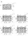
<第1実施形態>
本発明の第1実施形態にかかるインダクタ部品1について、図1および図2を参照して説明する。なお、図1(a)はインダクタ部品1の平面図、(b)〜(e)はインダクタ部品1の断面図、図2はインダクタ部品1の製造工程を示す図である。<First Embodiment>
An inductor component 1 according to a first embodiment of the present invention will be described with reference to FIGS. 1 and 2. 1A is a plan view of the inductor component 1, FIGS. 1B to 1E are cross-sectional views of the inductor component 1, and FIG. 2 is a diagram illustrating a manufacturing process of the inductor component 1.
この実施形態にかかるインダクタ部品1は、図1に示すように、樹脂層2と、樹脂層2の上面2aに積層された保護膜4と、樹脂層2の内部に立設された2本の金属ピン5と、樹脂層2の上面2aに配置されて両金属ピン5の上端面5a同士を接続する金属板6とを備え、両金属ピン5と金属板6とでインダクタ電極7を構成している。
As shown in FIG. 1, the inductor component 1 according to this embodiment includes a
樹脂層2は、例えば、エポキシ樹脂などの熱硬化性樹脂とフェライト粉末などの磁性体フィラーとが混合された磁性体含有樹脂により形成される。なお、磁性体含有樹脂を構成する樹脂は、熱硬化型に限られるものではなく、例えば、光硬化型樹脂であってもよい。また、磁性体フィラーを含有しない構成であってもよい。
The
両金属ピン5は、上端面5a(本発明の「金属ピンの端面」に相当)が樹脂層2の上面2a(本発明の「樹脂層の主面」に相当)に露出し、下端面5bが樹脂層2の下面2bから露出するように樹脂層2の内部に立設されている。
Both
また、金属ピン5は、Cu、Cu−Ni合金、Cu−Fe合金などのCu合金、Fe、Au、Ag、Alなどの材質により形成される。このような金属ピン5は、例えば、所望の直径を有し、円形状または多角形状の断面形状を有する金属導体の線材が所定の長さでせん断加工されて形成される。すなわち、インダクタ部品1が備える両金属ピン5は、ビア導体やビアフィルめっきなどで形成された層間接続導体のように、導電性ペーストの硬化物、めっきにより金属材料が所定の形状となるまで成長しためっき成長物、金属粉末の焼結体などとは異なる部材で形成されている。なお、本実施形態では金属ピン5は2本としているが、金属ピン5の本数は適宜変更可能である。また、両金属ピン5の下端面5bは、外部電極として使用することもできる。
The
また、図1(b)に示すように、樹脂層2の上面2aにおいて、両金属ピン5の上端面5aの周縁に凹部8が形成されている。この場合、両金属ピン5それぞれは、樹脂層2の上面2aのうちの当該金属ピン5の上端面5aの周縁部に対して、当該上端面5aが突出して配置されているともいえる。このような凹部8は、両金属ピン5の上端面5aの周縁にレーザー光を照射することにより形成できる。
Further, as shown in FIG. 1B, a
なお、図1(c)〜(e)に示すように、いずれも中央部に金属ピン5の上端部が配置された、円錐台状の凹部8a(図1(c)参照)、円柱状の凹部8b(図1(d)参照)、すり鉢状の凹部8c(図1(e)参照)のように凹部の形状が異なっていてもよい。また、本実施形態では、凹部8、8a〜8cは金属ピン5の上端面5aの周縁に形成されているが、凹部8、8a〜8cは上端面5aの少なくとも一部に対して形成されていればよい。また、凹部8、8a〜8cの形成はレーザー光の照射による方法のほか、樹脂硬化時の型押しによる形成も可能である。
In addition, as shown to FIG.1 (c)-(e), all are the truncated cone-shaped recessed
金属板6は、例えば、リードフレームのように薄板状の金属材料を所定の配線パターンの形状に加工したもので、樹脂層2の上面2aにおいて、両金属ピン5の上端面5a同士を接続する。そして、このように接続された両金属ピン5および金属板6が、樹脂層2の内部でインダクタ素子として機能する。なお、本実施形態では、金属板6はコ字状(図1(a)参照)に形成されているが、金属板6の形状はこれに限られるものではない。
The
保護膜4は、例えば、エポキシ樹脂やポリイミドなどで形成され、樹脂層2の上面2aに積層されることで金属板6を被覆する。
The protective film 4 is formed of, for example, epoxy resin or polyimide, and covers the
(インダクタ部品の製造方法)
次に、この実施形態にかかるインダクタ部品1の製造方法について、図2を参照して説明する。なお、以下の説明では、説明を容易なものとするため、1個のインダクタ部品1を製造する例を挙げて説明を行う。なお、以下で説明する製造方法と同じ要領で複数のインダクタ部品1を一括して形成し、その後に、それぞれのインダクタ部品1ごとに個片化することによって複数のインダクタ部品1を同時に製造してもよい。(Manufacturing method of inductor parts)
Next, a method for manufacturing the inductor component 1 according to this embodiment will be described with reference to FIG. In the following description, for ease of explanation, an example in which one inductor component 1 is manufactured will be described. In addition, a plurality of inductor components 1 are collectively formed in the same manner as the manufacturing method described below, and then the plurality of inductor components 1 are manufactured simultaneously by separating each inductor component 1 into individual pieces. Also good.
まず、2本の金属ピン5を用意し、転写板(図示省略)などの所定の位置に立設したあと、磁性体含有樹脂により両金属ピン5を被覆し、樹脂を熱硬化することによって、樹脂層2を形成する。次に、転写板を除去した後、樹脂層2の上面2aおよび下面2bの樹脂を研磨または研削して、両金属ピン5の上端面5aおよび下端面5bを樹脂層2の上面2aおよび下面2bにそれぞれ露出させる(図2(a)参照)。なお、樹脂量の調整により、研磨または研削による両金属ピン5の両端面5a、5bを露出させる工程が不要になる場合もある。
First, after preparing two
次に、図2(b)に示すように、両金属ピン5の上端面5aの周縁にレーザー光を照射し、凹部8を形成する。レーザー光は、金属ピン5で反射する特性を有するため、金属ピン5自体は損傷のない状態で残る。そのため、樹脂層2の金属ピン5の上端面5aの周囲に容易に凹部8を形成することができる。なお、レーザー光の条件によっては、金属ピン5の一部が除去される場合もあるが、この場合にも、樹脂層2のほうが金属ピン5よりも深く除去される。したがって、樹脂層2のうち金属ピン5の上端面5aの周縁に位置する部分には、凹部が形成される。
Next, as shown in FIG. 2 (b), the peripheral edge of the
次に、図2(c)に示すように、支持材9に取着された、所定の配線パターンの形状に加工された金属板6を用意し、金属板6と両金属ピン5の上端面5aとを超音波により接合してインダクタ電極7を形成する。その後、図2(d)に示すように、支持材9を除去してインダクタ部品1が完成する。金属板6は、例えば平板状の金属の板をエッチングなどでパターンニングすることで形成される。なお、金属板6と両金属ピン5の上端面5aとの接合は、半田を用いて行ってもよい。半田接合の場合、凹部8が半田受けとなり、金属ピン5と金属板6の接合部以外の領域に半田が広がるのを防止できる。さらに、金属板6と金属ピン5との接合性を上げる為に、金属ピン5と金属板6との間に半田を配置した状態で、超音波接合を行っても良い。この場合、超音波接合における半田と金属ピンの接合性が更に向上し、また凹部8が半田受けとなり半田の広がりを防止する事が出来る。
Next, as shown in FIG. 2 (c), a
上記した実施形態によれば、リードフレーム等の金属板6と金属ピン5とでインダクタ電極7を構成することにより、導電性ペーストやめっきで形成される従来の構成と比較して、インダクタ電極7の低抵抗化が可能になる。また、従来の構成と比較して、インダクタ電極7の主面上に形成された部分と樹脂層2内部に形成された部分の接続抵抗を下げることができるとともに、両者の接合部での発熱を抑制することができる。さらに、導電性ペーストやめっきを使用してインダクタ電極を形成する場合に比べて、短期間での製造が可能であり、製造コストの削減も可能となる。また、両金属ピン5の上端面5aは、樹脂層2の上面2aのうち金属ピン5の端面の周縁に対して突出して配設されるため、超音波接合時の振動エネルギーが樹脂層2に伝達されるのを抑えることができる。そのため、金属ピン5と金属板6との接合が確実になり、接合強度を高めることができる。
According to the above-described embodiment, the
(金属ピンと金属板との接合部の変形例)
両金属ピン5と金属板6との接合部の変形例について、図3を参照して説明する。なお、図3(a)はインダクタ部品1aの断面図、図3(b)はインダクタ部品1aの断面図である。(Modification of the joint between the metal pin and the metal plate)
A modification of the joint between the
図3(a)および(b)に示すように、両金属ピン5の上端面5aの周縁に形成した凹部8、8a〜8cの深さや、超音波接合時のエネルギーの強さを調整することにより、金属板6の一部または全部が各樹脂層2の凹部8に侵入した状態で金属ピン5に接続される構成であってもよい。
As shown in FIGS. 3 (a) and 3 (b), the depth of the
図3(a)は、超音波接合時の振動エネルギーにより、金属板6の一部が樹脂層2の凹部8に侵入している様子を表している。両金属ピン5と金属板6とでは、両金属ピン5のほうが変形しにくいため、両金属ピン5の上端面5aが金属板6に食い込む形状となる。また、図3(b)は、両金属ピン5の上端面5a上に金属板6が略存在せず、金属ピン5の側面のうち上端面5a側の端部に金属板6が接している様子を表している。
FIG. 3A shows a state in which a part of the
両金属ピン5と金属板6との接合部を上記のような形状に形成することで、当該接合部の接合強度をより高めることができる。
By forming the joint portion between both the
<第2実施形態>
本発明の第2実施形態にかかるインダクタ部品1bについて、図4を参照して説明する。なお、図4(a)および(b)はインダクタ部品1bの断面図である。Second Embodiment
An
この実施形態にかかるインダクタ部品1bが、図1および図2を参照して説明した第1実施形態のインダクタ部品1と異なるところは、両金属ピン5の上端面5aを含む端部が樹脂層2の上面2aから突出している点である。その他の構成は、第1実施形態のインダクタ部品1と同じであるため、同一符号を付すことにより説明を省略する。
The
この実施形態では、両金属ピン5を樹脂層2に配置する工程において、両金属ピン5の上端面5aを含む端部が樹脂の表面から突出した状態で樹脂を硬化させることにより、形成することができる。図4(a)に示すように、両金属ピン5だけが突出していてもよいし、図4(b)に示すように、両金属ピン5の上端面5aに向かって樹脂層2の上面2aに斜面が形成されていてもよい。
In this embodiment, in the step of arranging both
(インダクタ部品の製造方法)
次に、この発明の第2実施形態にかかるインダクタ部品1bの製造方法について、図5を参照して説明する。なお、以下の説明では、説明を容易なものとするため、1個のインダクタ部品1bを製造する例を挙げて説明を行う。なお、以下で説明する製造方法と同じ要領で複数のインダクタ部品1bを一括して形成し、その後に、それぞれのインダクタ部品1bごとに個片化することによって複数のインダクタ部品1bを同時に製造してもよい。(Manufacturing method of inductor parts)
Next, a method for manufacturing the
まず、図5(a)に示すように、その一方主面に粘着層(図示省略)が形成された転写板10を用意し、2本の金属ピン5の上端面5aを粘着層に取着することにより、両金属ピン5を転写板10の一方主面上の所定の位置に立設する。次に、図5(b)に示すように、転写板10に立設された両金属ピン5を、両金属ピン5の端部が樹脂の表面から露出するように、ダム材11に充填された未硬化の磁性体含有樹脂に浸漬させ、樹脂を熱硬化することによって、樹脂層2を形成する。
First, as shown in FIG. 5A, a
続いて、図5(c)に示すように、ダム材11を除去した後、図5(d)のように転写板10を両金属ピン5の上端面5aより剥離する。さらに、図5(e)に示すように、樹脂層2の下面(保護膜4と対抗する面との反対面)の樹脂を研磨または研削により除去して、両金属ピンの下端面5bを樹脂層2の表面に露出させる。なお、樹脂量の調整により、研磨または研削による金属ピン5の下端面5bを露出させる工程が不要な場合もある。
Subsequently, as shown in FIG. 5C, after removing the
次に、図5(f)に示すように、支持材9に取着された、所定の配線パターンの形状に加工された金属板6を用意し、金属板6と両金属ピン5の上端面5aとを超音波により接合してインダクタ電極7を形成する。その後、図5(g)に示すように、支持材9を除去してインダクタ部品1bが完成する。なお、金属板6と両金属ピン5の上端面5aとの接合は、半田を用いて行ってもよい。
Next, as shown in FIG. 5 (f), a
この実施形態によると、両金属ピン5の上端面5aが、樹脂層2の上面2aから突出しているため、超音波接合の際の振動エネルギーを、両金属ピン5と金属板6との接合部に効率よく印加できるだけでなく、両金属ピン5と金属板6との接合時の位置合わせが容易になる。
According to this embodiment, since the upper end surfaces 5 a of both
<第3実施形態>
本発明の第3実施形態にかかるインダクタ部品1cについて、図6を参照して説明する。なお、図6(a)はインダクタ部品1cの平面図、図6(b)〜(e)はインダクタ部品1cの断面図である。<Third Embodiment>
An
この実施形態にかかるインダクタ部品1cが、第1実施形態及び第2実施形態と異なるところは、インダクタ部品1cが、樹脂層2に埋設された環状のコイルコア20を備えていることと、インダクタ電極7がコイルコア20の周囲を螺旋状に巻回することでトロイダルコイルを形成していることである。以下の説明においては、上記した第1実施形態および第2実施形態と異なる点を中心に説明し、上記した第1実施形態及び第2実施形態と同様の構成については、同一符号を付すことにより説明を省略する。
The
図6(a)に示すように、インダクタ電極7が複数の金属ピン5と、いずれも短冊状の複数の金属板6、6aとで構成される。具体的には、各金属ピン5は、コイルコア20の内周に沿って配列されたものと、これらと複数の対をなすように外周に沿って配列されたものとで構成される。各金属ピン5は、いずれも上端面5aが樹脂層2の上面2aに露出し、下端面5bが樹脂層2の下面2bに露出した状態で樹脂層2の内部に立設される。樹脂層2の上面2aに配置された複数の金属板6は、いずれも一端がコイルコア20の内周側に配置されるとともに、他端が外周側に配置され、対を成す内周側の金属ピン5と外周側の金属ピン5の上端面5a同士を接続する。一方、樹脂層2の下面2bに配置された複数の金属板6aは、いずれも一端がコイルコア20の内周側に配置されるとともに、他端が外周側に配置され、内周側に配置された一の金属ピン5と、この金属ピン5と対をなす外周側の金属ピン5の所定側(この実施形態では、反時計方向)に隣接した外周側の金属ピン5の下端面5b同士を接続する。このような接続構成により、インダクタ電極7が環状のコイルコア20の周囲を螺旋状に巻回して成るトロイダルコイルが形成される。
As shown in FIG. 6A, the
また、樹脂層2の下面2bにも第1実施形態と同様の保護膜4が配置される(図6(b)〜(e)参照)。また、樹脂層2の下面2b側に配置された各金属板6aとコイルコア20との間には、絶縁物21が配置されている(図6(b)〜(d)参照)。
Moreover, the protective film 4 similar to 1st Embodiment is arrange | positioned also on the
また、この実施形態では、樹脂層2は、磁性体フィラーを含んでおらず、エポキシ樹脂等の一般的な熱硬化性の樹脂により形成されている。なお、上記した実施形態と同様に、樹脂層2の材質は、エポキシ樹脂等の熱硬化性の樹脂に限定されるものではない。
In this embodiment, the
また、この実施形態では、両金属ピン5の両端面5a、5bと、金属板6、6aとの接合を確実に行うため、両金属ピン5の両端面5a、5bと周縁の樹脂との位置関係は第1実施形態のインダクタ部品1およびその変形例と同様に、図6(b)〜(e)のいずれかで構成される。
Further, in this embodiment, the positions of both end faces 5a, 5b of both
例えば、図6(b)では、各金属ピン5の上端面5aを含む端部が樹脂層2の上面2aから突出した状態で設けられる。また、樹脂層2の下面2b側は、金属板6aの一部が樹脂層2の内側に入り込んだ状態で金属ピン5の下端面5bと接続されている。このとき、各金属ピン5の下端面5bが金属板6aに食い込んだ状態で両者が接続される。
For example, in FIG. 6B, the end including the
また、図6(c)では、図1(b)と同様、各金属ピン5の両端面5a、5bの周縁に凹部8が形成されている。また、図6(d)では、図1(e)と同様、各金属ピン5それぞれの両端面5a、5bの周囲にすり鉢状の凹部8cが形成されている。また、図6(e)では、図3(a)と同様、金属板6、6aの一部が樹脂層2内部に侵入し、両金属ピン5の両端面5a、5bがそれぞれ金属板6、6aに食い込んだ状態となっている。
Moreover, in FIG.6 (c), the recessed
インダクタ部品1cは、図2を参照して説明した製造方法と同じ要領で製造することができる。この場合、図2(a)に示す工程において、金属ピン5を樹脂で被覆する際に、各金属ピン5の間にコイルコア20を配置したあと樹脂層2を形成し、その後は同じ要領でインダクタ部品1cを製造するとよい。
The
上記した実施形態によれば、インダクタ電極7がトロイダルコイルを形成する構成において、第1実施形態と同様の効果を得ることができる。
According to the above-described embodiment, the same effect as that of the first embodiment can be obtained in the configuration in which the
なお、本発明は上記した各実施形態に限定されるものではなく、その趣旨を逸脱しない限りにおいて、上記したもの以外に種々の変更を行うことが可能である。例えば、上記した第3実施形態において、コイルコア20を配置しなくてもよい。
The present invention is not limited to the above-described embodiments, and various modifications other than those described above can be made without departing from the spirit of the present invention. For example, in the third embodiment described above, the
本発明は、樹脂層に設けられたインダクタを備えるインダクタ部品およびその製造方法に広く適用することができる。 The present invention can be widely applied to an inductor component including an inductor provided in a resin layer and a manufacturing method thereof.
1、1a〜1c インダクタ部品
2 樹脂層
5 金属ピン
6、6a 金属板
7 インダクタ電極
8、8a〜8c 凹部
DESCRIPTION OF
Claims (4)
インダクタ電極とを備え、
前記インダクタ電極は、
端面が前記樹脂層の主面に露出した状態で前記樹脂層内に立設された金属ピンと、
前記金属ピンの前記端面に接する配線用の金属板とを有し、
前記樹脂層の前記主面のうち、前記金属ピンの前記端面の周縁の少なくとも一部に凹部が形成されて、前記金属ピンは、前記樹脂層の前記主面のうち前記金属ピンの前記端面の周縁の少なくとも一部に対して、前記端面が突出して配設され、
前記金属ピンの前記端面が前記金属板に超音波接合されることを特徴とするインダクタ部品。 A resin layer;
An inductor electrode,
The inductor electrode is
A metal pin erected in the resin layer with the end face exposed at the main surface of the resin layer;
A wiring metal plate in contact with the end face of the metal pin,
A recess is formed in at least a part of a peripheral edge of the end surface of the metal pin in the main surface of the resin layer, and the metal pin is formed on the end surface of the metal pin in the main surface of the resin layer. The end face is disposed so as to protrude from at least a part of the periphery,
The inductor component, wherein the end face of the metal pin is ultrasonically bonded to the metal plate.
前記樹脂層の前記主面における前記金属ピンの前記端面の周縁の少なくとも一部にレーザー光を照射して凹部を形成する工程と、
前記金属ピンの前記端面と配線用の金属板とを接合することにより、前記金属ピンと前記金属板とを有するインダクタ電極を形成する工程と
を備え、
前記インダクタ電極を形成する工程において、前記金属ピンの前記端面と前記金属板とを超音波により接合することを特徴とするインダクタ部品の製造方法。 Preparing a metal pin erected in the resin layer in a state where the end surface is exposed on the main surface of the resin layer;
Irradiating at least part of the peripheral edge of the end surface of the metal pin on the main surface of the resin layer to form a recess;
Forming an inductor electrode having the metal pin and the metal plate by joining the end face of the metal pin and a metal plate for wiring ; and
In the step of forming the inductor electrode, the end surface of the metal pin and the metal plate are joined by ultrasonic waves .
Applications Claiming Priority (3)
| Application Number | Priority Date | Filing Date | Title |
|---|---|---|---|
| JP2016000869 | 2016-01-06 | ||
| JP2016000869 | 2016-01-06 | ||
| PCT/JP2017/000078 WO2017119423A1 (en) | 2016-01-06 | 2017-01-05 | Inductor component and inductor component production method |
Publications (2)
| Publication Number | Publication Date |
|---|---|
| JPWO2017119423A1 JPWO2017119423A1 (en) | 2018-11-08 |
| JP6579201B2 true JP6579201B2 (en) | 2019-09-25 |
Family
ID=59274439
Family Applications (1)
| Application Number | Title | Priority Date | Filing Date |
|---|---|---|---|
| JP2017560393A Active JP6579201B2 (en) | 2016-01-06 | 2017-01-05 | Inductor component and method of manufacturing inductor component |
Country Status (3)
| Country | Link |
|---|---|
| US (1) | US11373796B2 (en) |
| JP (1) | JP6579201B2 (en) |
| WO (1) | WO2017119423A1 (en) |
Families Citing this family (3)
| Publication number | Priority date | Publication date | Assignee | Title |
|---|---|---|---|---|
| FR3083365B1 (en) * | 2018-06-27 | 2020-07-17 | Safran Electronics & Defense | TRANSFORMER HAVING A PRINTED CIRCUIT |
| JP7115453B2 (en) * | 2019-10-02 | 2022-08-09 | 味の素株式会社 | Wiring board having inductor function and manufacturing method thereof |
| CN112864136B (en) * | 2021-01-14 | 2023-04-18 | 长鑫存储技术有限公司 | Semiconductor structure and manufacturing method thereof |
Family Cites Families (10)
| Publication number | Priority date | Publication date | Assignee | Title |
|---|---|---|---|---|
| US7196607B2 (en) * | 2004-03-26 | 2007-03-27 | Harris Corporation | Embedded toroidal transformers in ceramic substrates |
| EP2109867A4 (en) * | 2007-01-11 | 2014-12-24 | Keyeye Comm | Wideband planar transformer |
| KR20130076286A (en) | 2011-12-28 | 2013-07-08 | 삼성전기주식회사 | Printed circuit board and method for manufacturing the same |
| US9761553B2 (en) * | 2012-10-19 | 2017-09-12 | Taiwan Semiconductor Manufacturing Company Limited | Inductor with conductive trace |
| US10141107B2 (en) * | 2013-10-10 | 2018-11-27 | Analog Devices, Inc. | Miniature planar transformer |
| JP6226059B2 (en) * | 2014-03-04 | 2017-11-08 | 株式会社村田製作所 | Coil component, coil module, and method of manufacturing coil component |
| JP6217841B2 (en) * | 2014-03-18 | 2017-10-25 | 株式会社村田製作所 | Module and method for manufacturing the module |
| JP6323553B2 (en) * | 2014-06-11 | 2018-05-16 | 株式会社村田製作所 | Coil parts |
| GB2535763B (en) * | 2015-02-26 | 2018-08-01 | Murata Manufacturing Co | An embedded magnetic component device |
| JP6551546B2 (en) * | 2016-01-27 | 2019-07-31 | 株式会社村田製作所 | Inductor component and method of manufacturing the same |
-
2017
- 2017-01-05 JP JP2017560393A patent/JP6579201B2/en active Active
- 2017-01-05 WO PCT/JP2017/000078 patent/WO2017119423A1/en active Application Filing
-
2018
- 2018-07-05 US US16/027,504 patent/US11373796B2/en active Active
Also Published As
| Publication number | Publication date |
|---|---|
| WO2017119423A1 (en) | 2017-07-13 |
| US11373796B2 (en) | 2022-06-28 |
| US20180315543A1 (en) | 2018-11-01 |
| JPWO2017119423A1 (en) | 2018-11-08 |
Similar Documents
| Publication | Publication Date | Title |
|---|---|---|
| CN111430128B (en) | Coil component | |
| JP6244147B2 (en) | Manufacturing method of semiconductor device | |
| JP6125332B2 (en) | Semiconductor device | |
| JP6579201B2 (en) | Inductor component and method of manufacturing inductor component | |
| JP6606331B2 (en) | Electronic equipment | |
| JP2011035056A (en) | Semiconductor chip built-in package and method of manufacturing the same, and package-on-package semiconductor device and method of manufacturing the same | |
| JP2000138313A (en) | Semiconductor device and its manufacture | |
| JP5406572B2 (en) | Electronic component built-in wiring board and manufacturing method thereof | |
| JP6265275B2 (en) | Inductor component and method of manufacturing inductor component | |
| US9972560B2 (en) | Lead frame and semiconductor device | |
| JP7413485B2 (en) | semiconductor equipment | |
| US8507805B2 (en) | Wiring board for semiconductor devices, semiconductor device, electronic device, and motherboard | |
| JP6365692B2 (en) | Coil parts | |
| JP5803345B2 (en) | Semiconductor chip manufacturing method, circuit package and manufacturing method thereof | |
| JP6428931B2 (en) | Inductor parts | |
| JP2007089316A (en) | Microminiature power conversion device and manufacturing method therefor | |
| JP6274135B2 (en) | Coil module | |
| JP2020129637A (en) | Electronic device and manufacturing method thereof | |
| JP2017112325A (en) | Semiconductor device and manufacturing method of the same | |
| JP4010311B2 (en) | Semiconductor device and manufacturing method of semiconductor device | |
| JP5995579B2 (en) | Semiconductor light emitting device and manufacturing method thereof | |
| JP6534700B2 (en) | Semiconductor device manufacturing method | |
| JP2017183571A (en) | Manufacturing method of semiconductor device | |
| JP2016046509A (en) | Printed wiring board and semiconductor package | |
| JP2016139729A (en) | Electronic device and method of manufacturing electronic device |
Legal Events
| Date | Code | Title | Description |
|---|---|---|---|
| A621 | Written request for application examination |
Free format text: JAPANESE INTERMEDIATE CODE: A621 Effective date: 20180628 |
|
| A131 | Notification of reasons for refusal |
Free format text: JAPANESE INTERMEDIATE CODE: A131 Effective date: 20181127 |
|
| A521 | Request for written amendment filed |
Free format text: JAPANESE INTERMEDIATE CODE: A523 Effective date: 20190124 |
|
| A131 | Notification of reasons for refusal |
Free format text: JAPANESE INTERMEDIATE CODE: A131 Effective date: 20190528 |
|
| A521 | Request for written amendment filed |
Free format text: JAPANESE INTERMEDIATE CODE: A523 Effective date: 20190722 |
|
| TRDD | Decision of grant or rejection written | ||
| A01 | Written decision to grant a patent or to grant a registration (utility model) |
Free format text: JAPANESE INTERMEDIATE CODE: A01 Effective date: 20190730 |
|
| A61 | First payment of annual fees (during grant procedure) |
Free format text: JAPANESE INTERMEDIATE CODE: A61 Effective date: 20190812 |
|
| R150 | Certificate of patent or registration of utility model |
Ref document number: 6579201 Country of ref document: JP Free format text: JAPANESE INTERMEDIATE CODE: R150 |