JP6579201B2 - インダクタ部品およびインダクタ部品の製造方法 - Google Patents
インダクタ部品およびインダクタ部品の製造方法 Download PDFInfo
- Publication number
- JP6579201B2 JP6579201B2 JP2017560393A JP2017560393A JP6579201B2 JP 6579201 B2 JP6579201 B2 JP 6579201B2 JP 2017560393 A JP2017560393 A JP 2017560393A JP 2017560393 A JP2017560393 A JP 2017560393A JP 6579201 B2 JP6579201 B2 JP 6579201B2
- Authority
- JP
- Japan
- Prior art keywords
- metal
- resin layer
- metal pin
- inductor
- metal plate
- Prior art date
- Legal status (The legal status is an assumption and is not a legal conclusion. Google has not performed a legal analysis and makes no representation as to the accuracy of the status listed.)
- Active
Links
- 238000004519 manufacturing process Methods 0.000 title description 23
- 229910052751 metal Inorganic materials 0.000 claims description 213
- 239000002184 metal Substances 0.000 claims description 213
- 229920005989 resin Polymers 0.000 claims description 107
- 239000011347 resin Substances 0.000 claims description 107
- 230000002093 peripheral effect Effects 0.000 claims description 24
- 238000005304 joining Methods 0.000 claims description 20
- 229910000679 solder Inorganic materials 0.000 claims description 13
- 230000001678 irradiating effect Effects 0.000 claims description 3
- 239000010410 layer Substances 0.000 description 73
- 238000007747 plating Methods 0.000 description 10
- 238000000034 method Methods 0.000 description 9
- 239000004020 conductor Substances 0.000 description 7
- 238000012986 modification Methods 0.000 description 5
- 230000004048 modification Effects 0.000 description 5
- 229920001187 thermosetting polymer Polymers 0.000 description 5
- 239000003822 epoxy resin Substances 0.000 description 4
- 239000000463 material Substances 0.000 description 4
- 229920000647 polyepoxide Polymers 0.000 description 4
- 230000001681 protective effect Effects 0.000 description 4
- 239000012212 insulator Substances 0.000 description 3
- 239000012762 magnetic filler Substances 0.000 description 3
- 238000005498 polishing Methods 0.000 description 3
- 239000012790 adhesive layer Substances 0.000 description 2
- 229910045601 alloy Inorganic materials 0.000 description 2
- 239000000956 alloy Substances 0.000 description 2
- 239000007769 metal material Substances 0.000 description 2
- 239000000843 powder Substances 0.000 description 2
- 238000003892 spreading Methods 0.000 description 2
- 239000000126 substance Substances 0.000 description 2
- 229910000881 Cu alloy Inorganic materials 0.000 description 1
- 229910002482 Cu–Ni Inorganic materials 0.000 description 1
- 229910017827 Cu—Fe Inorganic materials 0.000 description 1
- 239000004642 Polyimide Substances 0.000 description 1
- 230000005540 biological transmission Effects 0.000 description 1
- 229910052802 copper Inorganic materials 0.000 description 1
- 238000010586 diagram Methods 0.000 description 1
- 238000007598 dipping method Methods 0.000 description 1
- 230000000694 effects Effects 0.000 description 1
- 238000005530 etching Methods 0.000 description 1
- 230000020169 heat generation Effects 0.000 description 1
- 239000011229 interlayer Substances 0.000 description 1
- 150000002739 metals Chemical class 0.000 description 1
- 238000000059 patterning Methods 0.000 description 1
- 229920001721 polyimide Polymers 0.000 description 1
- 238000010008 shearing Methods 0.000 description 1
- 229910052709 silver Inorganic materials 0.000 description 1
- 239000000758 substrate Substances 0.000 description 1
- 238000004804 winding Methods 0.000 description 1
- 229910000859 α-Fe Inorganic materials 0.000 description 1
Images


Classifications
-
- H—ELECTRICITY
- H01—ELECTRIC ELEMENTS
- H01F—MAGNETS; INDUCTANCES; TRANSFORMERS; SELECTION OF MATERIALS FOR THEIR MAGNETIC PROPERTIES
- H01F17/00—Fixed inductances of the signal type
- H01F17/0006—Printed inductances
- H01F17/0013—Printed inductances with stacked layers
-
- H—ELECTRICITY
- H01—ELECTRIC ELEMENTS
- H01F—MAGNETS; INDUCTANCES; TRANSFORMERS; SELECTION OF MATERIALS FOR THEIR MAGNETIC PROPERTIES
- H01F27/00—Details of transformers or inductances, in general
- H01F27/28—Coils; Windings; Conductive connections
- H01F27/29—Terminals; Tapping arrangements for signal inductances
-
- H—ELECTRICITY
- H01—ELECTRIC ELEMENTS
- H01F—MAGNETS; INDUCTANCES; TRANSFORMERS; SELECTION OF MATERIALS FOR THEIR MAGNETIC PROPERTIES
- H01F17/00—Fixed inductances of the signal type
- H01F17/0006—Printed inductances
- H01F17/0033—Printed inductances with the coil helically wound around a magnetic core
-
- H—ELECTRICITY
- H01—ELECTRIC ELEMENTS
- H01F—MAGNETS; INDUCTANCES; TRANSFORMERS; SELECTION OF MATERIALS FOR THEIR MAGNETIC PROPERTIES
- H01F17/00—Fixed inductances of the signal type
- H01F17/04—Fixed inductances of the signal type with magnetic core
- H01F17/06—Fixed inductances of the signal type with magnetic core with core substantially closed in itself, e.g. toroid
- H01F17/062—Toroidal core with turns of coil around it
-
- H—ELECTRICITY
- H01—ELECTRIC ELEMENTS
- H01F—MAGNETS; INDUCTANCES; TRANSFORMERS; SELECTION OF MATERIALS FOR THEIR MAGNETIC PROPERTIES
- H01F27/00—Details of transformers or inductances, in general
- H01F27/28—Coils; Windings; Conductive connections
- H01F27/32—Insulating of coils, windings, or parts thereof
- H01F27/324—Insulation between coil and core, between different winding sections, around the coil; Other insulation structures
-
- H—ELECTRICITY
- H01—ELECTRIC ELEMENTS
- H01F—MAGNETS; INDUCTANCES; TRANSFORMERS; SELECTION OF MATERIALS FOR THEIR MAGNETIC PROPERTIES
- H01F41/00—Apparatus or processes specially adapted for manufacturing or assembling magnets, inductances or transformers; Apparatus or processes specially adapted for manufacturing materials characterised by their magnetic properties
- H01F41/02—Apparatus or processes specially adapted for manufacturing or assembling magnets, inductances or transformers; Apparatus or processes specially adapted for manufacturing materials characterised by their magnetic properties for manufacturing cores, coils, or magnets
- H01F41/04—Apparatus or processes specially adapted for manufacturing or assembling magnets, inductances or transformers; Apparatus or processes specially adapted for manufacturing materials characterised by their magnetic properties for manufacturing cores, coils, or magnets for manufacturing coils
- H01F41/041—Printed circuit coils
-
- H—ELECTRICITY
- H01—ELECTRIC ELEMENTS
- H01F—MAGNETS; INDUCTANCES; TRANSFORMERS; SELECTION OF MATERIALS FOR THEIR MAGNETIC PROPERTIES
- H01F17/00—Fixed inductances of the signal type
- H01F17/0006—Printed inductances
- H01F17/0013—Printed inductances with stacked layers
- H01F2017/002—Details of via holes for interconnecting the layers
Landscapes
- Engineering & Computer Science (AREA)
- Power Engineering (AREA)
- Microelectronics & Electronic Packaging (AREA)
- Manufacturing & Machinery (AREA)
- Coils Or Transformers For Communication (AREA)
- Manufacturing Cores, Coils, And Magnets (AREA)
- Coils Of Transformers For General Uses (AREA)
Description
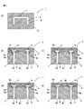
本発明の第1実施形態にかかるインダクタ部品1について、図1および図2を参照して説明する。なお、図1(a)はインダクタ部品1の平面図、(b)〜(e)はインダクタ部品1の断面図、図2はインダクタ部品1の製造工程を示す図である。
次に、この実施形態にかかるインダクタ部品1の製造方法について、図2を参照して説明する。なお、以下の説明では、説明を容易なものとするため、1個のインダクタ部品1を製造する例を挙げて説明を行う。なお、以下で説明する製造方法と同じ要領で複数のインダクタ部品1を一括して形成し、その後に、それぞれのインダクタ部品1ごとに個片化することによって複数のインダクタ部品1を同時に製造してもよい。
両金属ピン5と金属板6との接合部の変形例について、図3を参照して説明する。なお、図3(a)はインダクタ部品1aの断面図、図3(b)はインダクタ部品1aの断面図である。
本発明の第2実施形態にかかるインダクタ部品1bについて、図4を参照して説明する。なお、図4(a)および(b)はインダクタ部品1bの断面図である。
次に、この発明の第2実施形態にかかるインダクタ部品1bの製造方法について、図5を参照して説明する。なお、以下の説明では、説明を容易なものとするため、1個のインダクタ部品1bを製造する例を挙げて説明を行う。なお、以下で説明する製造方法と同じ要領で複数のインダクタ部品1bを一括して形成し、その後に、それぞれのインダクタ部品1bごとに個片化することによって複数のインダクタ部品1bを同時に製造してもよい。
本発明の第3実施形態にかかるインダクタ部品1cについて、図6を参照して説明する。なお、図6(a)はインダクタ部品1cの平面図、図6(b)〜(e)はインダクタ部品1cの断面図である。
2 樹脂層
5 金属ピン
6、6a 金属板
7 インダクタ電極
8、8a〜8c 凹部
Claims (4)
- 樹脂層と、
インダクタ電極とを備え、
前記インダクタ電極は、
端面が前記樹脂層の主面に露出した状態で前記樹脂層内に立設された金属ピンと、
前記金属ピンの前記端面に接する配線用の金属板とを有し、
前記樹脂層の前記主面のうち、前記金属ピンの前記端面の周縁の少なくとも一部に凹部が形成されて、前記金属ピンは、前記樹脂層の前記主面のうち前記金属ピンの前記端面の周縁の少なくとも一部に対して、前記端面が突出して配設され、
前記金属ピンの前記端面が前記金属板に超音波接合されることを特徴とするインダクタ部品。 - 前記凹部に半田が配置されていることを特徴とする請求項1に記載のインダクタ部品。
- 前記樹脂層の前記主面のうち、前記金属ピンの前記端面の周縁全部に凹部が形成されて、前記金属ピンの前記端面を含む端部が、前記樹脂層の前記主面から突出していることを特徴とする請求項1または2に記載のインダクタ部品。
- 端面が樹脂層の主面に露出した状態で当該樹脂層内に立設された金属ピンを準備する工程と、
前記樹脂層の前記主面における前記金属ピンの前記端面の周縁の少なくとも一部にレーザー光を照射して凹部を形成する工程と、
前記金属ピンの前記端面と配線用の金属板とを接合することにより、前記金属ピンと前記金属板とを有するインダクタ電極を形成する工程と
を備え、
前記インダクタ電極を形成する工程において、前記金属ピンの前記端面と前記金属板とを超音波により接合することを特徴とするインダクタ部品の製造方法。
Applications Claiming Priority (3)
| Application Number | Priority Date | Filing Date | Title |
|---|---|---|---|
| JP2016000869 | 2016-01-06 | ||
| JP2016000869 | 2016-01-06 | ||
| PCT/JP2017/000078 WO2017119423A1 (ja) | 2016-01-06 | 2017-01-05 | インダクタ部品およびインダクタ部品の製造方法 |
Publications (2)
| Publication Number | Publication Date |
|---|---|
| JPWO2017119423A1 JPWO2017119423A1 (ja) | 2018-11-08 |
| JP6579201B2 true JP6579201B2 (ja) | 2019-09-25 |
Family
ID=59274439
Family Applications (1)
| Application Number | Title | Priority Date | Filing Date |
|---|---|---|---|
| JP2017560393A Active JP6579201B2 (ja) | 2016-01-06 | 2017-01-05 | インダクタ部品およびインダクタ部品の製造方法 |
Country Status (3)
| Country | Link |
|---|---|
| US (1) | US11373796B2 (ja) |
| JP (1) | JP6579201B2 (ja) |
| WO (1) | WO2017119423A1 (ja) |
Families Citing this family (3)
| Publication number | Priority date | Publication date | Assignee | Title |
|---|---|---|---|---|
| FR3083365B1 (fr) * | 2018-06-27 | 2020-07-17 | Safran Electronics & Defense | Transformateur comportant un circuit imprime |
| JP7115453B2 (ja) * | 2019-10-02 | 2022-08-09 | 味の素株式会社 | インダクタ機能を有する配線基板及びその製造方法 |
| CN112864136B (zh) * | 2021-01-14 | 2023-04-18 | 长鑫存储技术有限公司 | 半导体结构及其制作方法 |
Family Cites Families (10)
| Publication number | Priority date | Publication date | Assignee | Title |
|---|---|---|---|---|
| US7196607B2 (en) * | 2004-03-26 | 2007-03-27 | Harris Corporation | Embedded toroidal transformers in ceramic substrates |
| EP2109867A4 (en) * | 2007-01-11 | 2014-12-24 | Keyeye Comm | BROADBAND planar transformers |
| KR20130076286A (ko) | 2011-12-28 | 2013-07-08 | 삼성전기주식회사 | 인쇄회로기판 및 그의 제조방법 |
| US9761553B2 (en) * | 2012-10-19 | 2017-09-12 | Taiwan Semiconductor Manufacturing Company Limited | Inductor with conductive trace |
| US10141107B2 (en) * | 2013-10-10 | 2018-11-27 | Analog Devices, Inc. | Miniature planar transformer |
| WO2015133361A1 (ja) * | 2014-03-04 | 2015-09-11 | 株式会社村田製作所 | コイル部品およびコイルモジュール、並びに、コイル部品の製造方法 |
| WO2015141434A1 (ja) * | 2014-03-18 | 2015-09-24 | 株式会社村田製作所 | モジュールおよびこのモジュールの製造方法 |
| WO2015190229A1 (ja) * | 2014-06-11 | 2015-12-17 | 株式会社村田製作所 | コイル部品 |
| GB2535763B (en) * | 2015-02-26 | 2018-08-01 | Murata Manufacturing Co | An embedded magnetic component device |
| JP6551546B2 (ja) * | 2016-01-27 | 2019-07-31 | 株式会社村田製作所 | インダクタ部品およびその製造方法 |
-
2017
- 2017-01-05 JP JP2017560393A patent/JP6579201B2/ja active Active
- 2017-01-05 WO PCT/JP2017/000078 patent/WO2017119423A1/ja active Application Filing
-
2018
- 2018-07-05 US US16/027,504 patent/US11373796B2/en active Active
Also Published As
| Publication number | Publication date |
|---|---|
| US20180315543A1 (en) | 2018-11-01 |
| WO2017119423A1 (ja) | 2017-07-13 |
| US11373796B2 (en) | 2022-06-28 |
| JPWO2017119423A1 (ja) | 2018-11-08 |
Similar Documents
| Publication | Publication Date | Title |
|---|---|---|
| CN111430128B (zh) | 线圈部件 | |
| JP6244147B2 (ja) | 半導体装置の製造方法 | |
| JP6125332B2 (ja) | 半導体装置 | |
| JP6579201B2 (ja) | インダクタ部品およびインダクタ部品の製造方法 | |
| JP6606331B2 (ja) | 電子装置 | |
| JP2011035056A (ja) | 半導体チップ内蔵パッケージ及びその製造方法、並びに、パッケージ・オン・パッケージ型半導体装置及びその製造方法 | |
| JP2000138313A (ja) | 半導体装置及びその製造方法 | |
| JP5406572B2 (ja) | 電子部品内蔵配線基板及びその製造方法 | |
| JP6265275B2 (ja) | インダクタ部品およびインダクタ部品の製造方法 | |
| US9972560B2 (en) | Lead frame and semiconductor device | |
| WO2014054451A1 (ja) | 半導体装置及びその製造方法 | |
| JP7413485B2 (ja) | 半導体装置 | |
| US8507805B2 (en) | Wiring board for semiconductor devices, semiconductor device, electronic device, and motherboard | |
| JP6365692B2 (ja) | コイル部品 | |
| JP5803345B2 (ja) | 半導体チップの製造方法、回路実装体及びその製造方法 | |
| JP6274135B2 (ja) | コイルモジュール | |
| JP6428931B2 (ja) | インダクタ部品 | |
| JP2020129637A (ja) | 電子装置及び電子装置の製造方法 | |
| JP2017112325A (ja) | 半導体装置及びその製造方法 | |
| JP4010311B2 (ja) | 半導体装置および半導体装置の製造方法 | |
| JP5995579B2 (ja) | 半導体発光装置及びその製造方法 | |
| JP6534700B2 (ja) | 半導体装置の製造方法 | |
| JP2017183571A (ja) | 半導体装置の製造方法 | |
| JP2016046509A (ja) | プリント配線板および半導体パッケージ | |
| JP2009152372A (ja) | プリント基板、半導体装置、及びこれらの製造方法 |
Legal Events
| Date | Code | Title | Description |
|---|---|---|---|
| A621 | Written request for application examination |
Free format text: JAPANESE INTERMEDIATE CODE: A621 Effective date: 20180628 |
|
| A131 | Notification of reasons for refusal |
Free format text: JAPANESE INTERMEDIATE CODE: A131 Effective date: 20181127 |
|
| A521 | Request for written amendment filed |
Free format text: JAPANESE INTERMEDIATE CODE: A523 Effective date: 20190124 |
|
| A131 | Notification of reasons for refusal |
Free format text: JAPANESE INTERMEDIATE CODE: A131 Effective date: 20190528 |
|
| A521 | Request for written amendment filed |
Free format text: JAPANESE INTERMEDIATE CODE: A523 Effective date: 20190722 |
|
| TRDD | Decision of grant or rejection written | ||
| A01 | Written decision to grant a patent or to grant a registration (utility model) |
Free format text: JAPANESE INTERMEDIATE CODE: A01 Effective date: 20190730 |
|
| A61 | First payment of annual fees (during grant procedure) |
Free format text: JAPANESE INTERMEDIATE CODE: A61 Effective date: 20190812 |
|
| R150 | Certificate of patent or registration of utility model |
Ref document number: 6579201 Country of ref document: JP Free format text: JAPANESE INTERMEDIATE CODE: R150 |