JP6517841B2 - Micro-acoustic device with improved temperature compensation - Google Patents
Micro-acoustic device with improved temperature compensation Download PDFInfo
- Publication number
- JP6517841B2 JP6517841B2 JP2016570834A JP2016570834A JP6517841B2 JP 6517841 B2 JP6517841 B2 JP 6517841B2 JP 2016570834 A JP2016570834 A JP 2016570834A JP 2016570834 A JP2016570834 A JP 2016570834A JP 6517841 B2 JP6517841 B2 JP 6517841B2
- Authority
- JP
- Japan
- Prior art keywords
- layer
- compensation layer
- compensation
- scf
- piezoelectric
- Prior art date
- Legal status (The legal status is an assumption and is not a legal conclusion. Google has not performed a legal analysis and makes no representation as to the accuracy of the status listed.)
- Expired - Fee Related
Links
- 239000000463 material Substances 0.000 claims description 41
- 239000000758 substrate Substances 0.000 claims description 20
- 150000001875 compounds Chemical class 0.000 claims description 17
- 229910052727 yttrium Inorganic materials 0.000 claims description 9
- VWQVUPCCIRVNHF-UHFFFAOYSA-N yttrium atom Chemical compound [Y] VWQVUPCCIRVNHF-UHFFFAOYSA-N 0.000 claims description 9
- OEKDNFRQVZLFBZ-UHFFFAOYSA-K scandium fluoride Chemical compound F[Sc](F)F OEKDNFRQVZLFBZ-UHFFFAOYSA-K 0.000 claims description 8
- 239000003989 dielectric material Substances 0.000 claims description 7
- 239000011521 glass Substances 0.000 claims description 7
- 229910016036 BaF 2 Inorganic materials 0.000 claims description 6
- 239000000126 substance Substances 0.000 claims description 5
- 150000004820 halides Chemical class 0.000 claims description 3
- 239000010457 zeolite Substances 0.000 claims description 2
- 239000003795 chemical substances by application Substances 0.000 claims 1
- 229910004298 SiO 2 Inorganic materials 0.000 description 14
- 230000008859 change Effects 0.000 description 8
- 239000008186 active pharmaceutical agent Substances 0.000 description 6
- 230000000694 effects Effects 0.000 description 5
- 230000000930 thermomechanical effect Effects 0.000 description 5
- 230000001419 dependent effect Effects 0.000 description 4
- 238000000151 deposition Methods 0.000 description 3
- -1 rare earth compound Chemical class 0.000 description 3
- 229910052761 rare earth metal Inorganic materials 0.000 description 3
- 238000002310 reflectometry Methods 0.000 description 3
- WSMQKESQZFQMFW-UHFFFAOYSA-N 5-methyl-pyrazole-3-carboxylic acid Chemical compound CC1=CC(C(O)=O)=NN1 WSMQKESQZFQMFW-UHFFFAOYSA-N 0.000 description 2
- 229910005793 GeO 2 Inorganic materials 0.000 description 2
- FTEFJLRQJWPKCG-UHFFFAOYSA-K [F-].[F-].[F-].[Y+3].[Sc+3] Chemical compound [F-].[F-].[F-].[Y+3].[Sc+3] FTEFJLRQJWPKCG-UHFFFAOYSA-K 0.000 description 2
- 230000008878 coupling Effects 0.000 description 2
- 238000010168 coupling process Methods 0.000 description 2
- 238000005859 coupling reaction Methods 0.000 description 2
- 239000013078 crystal Substances 0.000 description 2
- 230000007423 decrease Effects 0.000 description 2
- 230000008021 deposition Effects 0.000 description 2
- 239000007772 electrode material Substances 0.000 description 2
- 238000005516 engineering process Methods 0.000 description 2
- 230000006872 improvement Effects 0.000 description 2
- GQYHUHYESMUTHG-UHFFFAOYSA-N lithium niobate Chemical compound [Li+].[O-][Nb](=O)=O GQYHUHYESMUTHG-UHFFFAOYSA-N 0.000 description 2
- 238000004519 manufacturing process Methods 0.000 description 2
- 239000012528 membrane Substances 0.000 description 2
- 239000000203 mixture Substances 0.000 description 2
- 230000001590 oxidative effect Effects 0.000 description 2
- 230000000644 propagated effect Effects 0.000 description 2
- 239000004065 semiconductor Substances 0.000 description 2
- 239000007787 solid Substances 0.000 description 2
- 150000003623 transition metal compounds Chemical class 0.000 description 2
- XFXPMWWXUTWYJX-UHFFFAOYSA-N Cyanide Chemical compound N#[C-] XFXPMWWXUTWYJX-UHFFFAOYSA-N 0.000 description 1
- YCKRFDGAMUMZLT-UHFFFAOYSA-N Fluorine atom Chemical compound [F] YCKRFDGAMUMZLT-UHFFFAOYSA-N 0.000 description 1
- 229910004521 HfMo Inorganic materials 0.000 description 1
- 230000002411 adverse Effects 0.000 description 1
- 229910045601 alloy Inorganic materials 0.000 description 1
- 239000000956 alloy Substances 0.000 description 1
- 238000013459 approach Methods 0.000 description 1
- 230000008901 benefit Effects 0.000 description 1
- 238000013016 damping Methods 0.000 description 1
- 238000002474 experimental method Methods 0.000 description 1
- 229910052731 fluorine Inorganic materials 0.000 description 1
- 239000011737 fluorine Substances 0.000 description 1
- 229910052751 metal Inorganic materials 0.000 description 1
- 239000002184 metal Substances 0.000 description 1
- 150000001247 metal acetylides Chemical class 0.000 description 1
- 150000002739 metals Chemical class 0.000 description 1
- 238000000034 method Methods 0.000 description 1
- 230000004048 modification Effects 0.000 description 1
- 238000012986 modification Methods 0.000 description 1
- 150000004767 nitrides Chemical class 0.000 description 1
- 238000000059 patterning Methods 0.000 description 1
- 238000012545 processing Methods 0.000 description 1
- 230000009467 reduction Effects 0.000 description 1
- 238000010897 surface acoustic wave method Methods 0.000 description 1
- PBYZMCDFOULPGH-UHFFFAOYSA-N tungstate Chemical compound [O-][W]([O-])(=O)=O PBYZMCDFOULPGH-UHFFFAOYSA-N 0.000 description 1
- 229940105963 yttrium fluoride Drugs 0.000 description 1
- RBORBHYCVONNJH-UHFFFAOYSA-K yttrium(iii) fluoride Chemical compound F[Y](F)F RBORBHYCVONNJH-UHFFFAOYSA-K 0.000 description 1
Images


Classifications
-
- H—ELECTRICITY
- H03—ELECTRONIC CIRCUITRY
- H03H—IMPEDANCE NETWORKS, e.g. RESONANT CIRCUITS; RESONATORS
- H03H9/00—Networks comprising electromechanical or electro-acoustic elements; Electromechanical resonators
- H03H9/02—Details
- H03H9/02535—Details of surface acoustic wave devices
- H03H9/02818—Means for compensation or elimination of undesirable effects
- H03H9/02834—Means for compensation or elimination of undesirable effects of temperature influence
-
- H—ELECTRICITY
- H03—ELECTRONIC CIRCUITRY
- H03H—IMPEDANCE NETWORKS, e.g. RESONANT CIRCUITS; RESONATORS
- H03H9/00—Networks comprising electromechanical or electro-acoustic elements; Electromechanical resonators
- H03H9/02—Details
- H03H9/02007—Details of bulk acoustic wave devices
- H03H9/02086—Means for compensation or elimination of undesirable effects
- H03H9/02102—Means for compensation or elimination of undesirable effects of temperature influence
-
- H—ELECTRICITY
- H03—ELECTRONIC CIRCUITRY
- H03H—IMPEDANCE NETWORKS, e.g. RESONANT CIRCUITS; RESONATORS
- H03H9/00—Networks comprising electromechanical or electro-acoustic elements; Electromechanical resonators
- H03H9/02—Details
- H03H9/125—Driving means, e.g. electrodes, coils
- H03H9/145—Driving means, e.g. electrodes, coils for networks using surface acoustic waves
- H03H9/14544—Transducers of particular shape or position
-
- H—ELECTRICITY
- H03—ELECTRONIC CIRCUITRY
- H03H—IMPEDANCE NETWORKS, e.g. RESONANT CIRCUITS; RESONATORS
- H03H9/00—Networks comprising electromechanical or electro-acoustic elements; Electromechanical resonators
- H03H9/46—Filters
- H03H9/462—Microelectro-mechanical filters
Landscapes
- Physics & Mathematics (AREA)
- Acoustics & Sound (AREA)
- Surface Acoustic Wave Elements And Circuit Networks Thereof (AREA)
- Piezo-Electric Or Mechanical Vibrators, Or Delay Or Filter Circuits (AREA)
Description
たとえばSAWデバイス(SAW=surface acoustic wave)またはBAWデバイス(BAW=bulk acoustic wave)のような音響波で動作するデバイスの特性は、通常温度への依存性を示す。これよりたとえばタンタル酸リチウム(LT42°xy回転)ベースのSAWデバイスの中心周波数の温度係数(TCF)は、典型的にたとえば−40ppm/K付近となっている。ここで異なる基板は異なる温度係数を示す。 The characteristics of devices operating with acoustic waves, such as, for example, SAW devices (SAW = surface acoustic wave) or BAW devices (BAW = bulk acoustic wave), usually exhibit a dependence on temperature. From this, for example, the temperature coefficient (TCF) of the center frequency of a lithium tantalate (LT 42 ° xy rotation) based SAW device is typically around -40 ppm / K, for example. Here different substrates exhibit different temperature coefficients.
またこの材料の熱膨張は、密度ρの低下をもたらし、以下の関係
v = √(c/ρ)
により、その波動速度vに直接影響を与える。これにより、上記の熱膨張により増大した走行距離が、波に対する補償となる。しかしながら周波数への大部分の影響は、とりわけ、この温度と共に剛性cが変化することであり、この剛性は殆どの材料において、そしてこれより圧電材料においても、温度の上昇と共に低下する。さらに、圧電テンソルおよび基板の誘電率も温度依存性であり、そしてこれにより上記の温度係数の原因となっている。また電極材料の剛性の変化も、上記のTCFに影響を与えないわけではない。
Also, the thermal expansion of this material leads to a decrease in the density 、, and
v = ((c / ρ)
Directly affects the wave velocity v. Thereby, the travel distance increased by the above-mentioned thermal expansion serves as compensation for waves. However, most of the effect on frequency is, inter alia, the change in stiffness c with this temperature, which decreases with increasing temperature in most materials and also in piezoelectric materials. In addition, the dielectric constants of the piezoelectric tensor and the substrate are also temperature dependent, which is responsible for the above-mentioned temperature coefficient. Also, the change in rigidity of the electrode material does not necessarily affect the above-mentioned TCF.
以上より、たとえばフィルタの帯域幅を、上記の温度依存の変動の分だけ増大するために、音響波で動作するデバイスでの製造許容誤差が厳しくなるという問題が生じる。この問題は、隣接した周波数バンドでは、選択度を悪化させ、あるいは製造の際に、もはや要求されている仕様を満たさないデバイスの割合が大きくなるといったことをもたらす。他の仕様は、上記のTCFの補償のための対策無しには、もはや満足されない。 From the above, the problem arises that the manufacturing tolerances of devices operating with acoustic waves become tight, for example, by increasing the bandwidth of the filter by the above-mentioned temperature-dependent fluctuations. This problem leads to poor selectivity in adjacent frequency bands, or to a large proportion of devices that no longer meet the required specifications during manufacturing. Other specifications are no longer satisfied without measures for the above mentioned TCF compensation.
特許文献1には、音響波で動作するデバイスが提示されており、このデバイスは温度変化を低下させるための様々な対策(TK補償)、具体的には共振周波数の温度変化に対する対策が組み合わされている。このデバイスは、基板上面上に導電性のデバイスパターンを備え、その下面には補償層を備え、この補償層は、機械的な張力が生成され、すなわちこの張力が温度変化で形成されることで、この基板と機械的に堅く結合されている。 Patent Document 1 presents a device that operates with acoustic waves, and this device combines various measures to reduce temperature change (TK compensation), specifically measures against temperature change of resonant frequency. ing. The device comprises an electrically conductive device pattern on the upper surface of the substrate and a compensation layer on the lower surface, the compensation layer being produced by mechanical tensioning, ie this tension is formed by temperature change , Mechanically rigidly connected with this substrate.
他の対策として上記のデバイスパターンの上にSiO2層が配設される。このSiO2層は、その熱弾性特性が正の温度係数を備え、この正の温度係数は、大多数の基板材料、たとえばLTまたはLN(ニオブ酸リチウム)の負の温度係数を補償する。 As another measure, a SiO 2 layer is disposed on the above device pattern. This SiO 2 layer has a temperature coefficient whose thermoelastic properties have a positive temperature coefficient, which compensates for the negative temperature coefficient of the majority of substrate materials, for example LT or LN (lithium niobate).
この方法の欠点としては、上記の電極の必要とされる反射率が、重い電極でのみ得られることである。このことはとりわけSAWデバイスに対しては満足できるものではなく、そしていくつかの用途に対しては不十分である。さらにSiO2を用いた温度補償での欠点は、その温度補償特性に制限があることであり、SiO2の使用により、電気機械的カップリングおよび帯域幅の損失、減衰の増大、また望ましくない妨害モードの発生を甘受しなければならないことである。これは実効的に達成可能なTK補償を制限するものである。 The disadvantage of this method is that the required reflectivity of the above electrodes is obtained only with heavy electrodes. This is not particularly satisfactory for SAW devices and is insufficient for some applications. A further disadvantage of temperature compensation with SiO 2 is its limited temperature compensation properties, and the use of SiO 2 increases electromechanical coupling and bandwidth losses, increases attenuation, and unwanted disturbances. You have to accept the occurrence of the mode. This limits the TK compensation that can be effectively achieved.
たとえばGeO2、およびフッ素ドーピングまたはホウ素ドーピングされたSiO2のような、正の温度係数を有する他の層(複数)が、既に上記の温度依存特性の補償のために提案されている。 Other layers with positive temperature coefficients, such as, for example, GeO 2 and fluorine-doped or boron-doped SiO 2 have already been proposed for the compensation of the temperature-dependent properties described above.
本発明の課題は、上記の温度係数を補償するための新たな可能性あるいは材料を提示することであり、これによって上記の補償が改善されると共にこれに関係した欠点も低減される。 The object of the present invention is to present new possibilities or materials for compensating the above-mentioned temperature coefficient, which improves the above-mentioned compensation and reduces the drawbacks associated therewith.
この課題は、請求項1に記載の特徴を有するデバイスによって解決される。本発明の有利な実施形態がその下位請求項に示される。 This problem is solved by a device having the features of claim 1. Advantageous embodiments of the invention are indicated in the subclaims.
本発明は、負の熱膨張係数を有する材料の中に、その熱機械的特性が正の温度係数を備える多数の材料を見出すことができるという知見に基づいている。このような材料は、圧電材料では一般的に生じる、熱機械的特性の負の温度係数の補償のために使用することができる。 The invention is based on the finding that, among materials having a negative coefficient of thermal expansion, a large number of materials whose thermomechanical properties have a positive temperature coefficient can be found. Such materials can be used to compensate for the negative temperature coefficient of thermo-mechanical properties that commonly occurs in piezoelectric materials.
本発明では、音響波で動作するデバイス上に1つの補償層を取り付けることが提案され、この補償層は、少なくとも2つの元素の化合物をベースにした1つの誘電体材料を備え、この化合物は負の熱膨張係数を有する。 In the present invention, it is proposed to mount one compensation layer on a device operating with acoustic waves, this compensation layer comprising one dielectric material based on a compound of at least two elements, this compound being negative Have a coefficient of thermal expansion of
1つの実施形態によれば、この化合物は、1つの無機の遷移金属化合物または1つの希土類化合物である。しかしこの化合物は他の物質グループの化合物でもよい。 According to one embodiment, the compound is one inorganic transition metal compound or one rare earth compound. However, this compound may be a compound of another substance group.
このようなデバイスは、1つの圧電材料の少なくとも1つの層を備え、この圧電材料における音響波を励起するための1つの電極ペアを有している。上記の補償層にこの音響波のエネルギーの少なくとも一部が存在するように、この補償層がこのデバイス上に配設されている。この補償層は、この音響波が最初に生成される圧電層の比較的近くにあることが必要である。 Such a device comprises at least one layer of one piezoelectric material and has one electrode pair for exciting acoustic waves in this piezoelectric material. The compensation layer is disposed on the device such that at least a portion of the energy of the acoustic wave is present in the compensation layer. The compensation layer needs to be relatively close to the piezoelectric layer from which this acoustic wave is first generated.
たとえば誘電体の無機の遷移金属化合物および希土類化合物のグループから選択されている、負の熱膨張係数を有する材料は、驚くべきことにその弾性率Eが大きな正の温度係数を示し、また温度上昇と共に剛性が大きくなり、この剛性は今まで知られている材料の最も良いもの、たとえばこの用途のために今まで使用されてきたSiO2よりも大きいものである。この大きな剛性の変化によって、あるいはこれに付随する弾性率Eの正の温度係数によって、効果的な補償層を実現することに成功している。 For example, a material having a negative coefficient of thermal expansion, selected from the group of dielectric inorganic transition metal compounds and rare earth compounds, surprisingly exhibits a large positive temperature coefficient with its elastic modulus E and also a temperature rise With this, the stiffness increases, which is greater than the best of the materials known so far, for example the SiO 2 which has hitherto been used for this application. An effective compensation layer has been successfully realized by this large change in stiffness or by the positive temperature coefficient of the elastic modulus E accompanying this.
以上により、さらに周波数の温度係数を完全に補償することが可能であり、そしてさらに加えて、従来知られていた材料よりも小さな厚さの補償層を用いて補償することが可能である。ここで1つの薄い補償層を用いて、従来知られていた補償層の問題が同時に減少される。具体的には上記の圧電的なカップリングの減少、および上記の補償層で甘受しなければならなかった音響的減衰のような不利な効果が小さくなる。 From the above, it is also possible to fully compensate the temperature coefficient of the frequency, and in addition it is possible to compensate using a compensation layer of smaller thickness than previously known materials. Here, with one thin compensation layer, the problems of previously known compensation layers are simultaneously reduced. In particular, the disadvantageous effects such as the reduction of the piezoelectric coupling described above and the acoustic damping that has to be accepted in the compensation layer described above are reduced.
上記の見いだされた化合物のグループのさらなる利点は、これらの化合物を一般的に、半導体技術で知られた従来の堆積方法を用いて、制御されたやり方で取り付けることができるということである。以上により、音響波で動作するデバイス上に取り付けられるために、これらの化合物は処理技術的にも良好に適合したものである。 A further advantage of the group of compounds found above is that these compounds can generally be attached in a controlled manner using conventional deposition methods known in semiconductor technology. By virtue of the above, these compounds are also well suited in terms of processing technology to be mounted on devices operating with acoustic waves.
本発明の1つの実施形態においては、上記の補償層は、上記の圧電材料の層上に直接取り付けられる。電極(複数)および補償層は、この圧電層の同じ側に配設されていてよい。しかしながら、この補償層がこの圧電層の下側に配設され、そしてこれらの電極がこの圧電層の上側に配設されることも可能である。さらに、これらの電極を圧電層と補償層との間に設けることも可能である。もう1つの原理的に可能な変形例は、上記の電極(複数)を上記の補償層上に取り付けることであり、この補償層はまた上記の圧電層上に堆積されている。 In one embodiment of the present invention, the above-mentioned compensation layer is mounted directly on the above-mentioned layer of piezoelectric material. The electrodes and the compensation layer may be disposed on the same side of the piezoelectric layer. However, it is also possible that the compensation layer is disposed below the piezoelectric layer and the electrodes are disposed above the piezoelectric layer. Furthermore, it is also possible to provide these electrodes between the piezoelectric layer and the compensation layer. Another in principle possible variant is to attach the above mentioned electrodes (s) onto the above mentioned compensation layer, which is also deposited on the above mentioned piezoelectric layer.
本発明の1つの好ましい実施形態においては、上記の補償層は負の熱膨張係数を有する希土類化合物として、三フッ化スカンジウムScF3ベースのガラスを備える。この物質は十分に硬く、機械的に安定であり、そして良好に堆積することができる。 In one preferred embodiment of the present invention, the above-mentioned compensation layer comprises scandium trifluoride ScF 3 -based glass as a rare earth compound having a negative coefficient of thermal expansion. This material is sufficiently hard, mechanically stable and can be deposited well.
弾性率Eの特に大きな正の温度係数は、イットリウムドーピングされたSc(1-X)YXF3の化学式のフッ化スカンジウムを用いることで実現でき、ここで係数xで示されるイットリウムの割合は≦0.25であり、したがって0<x≦0.25となっている。 A particularly large positive temperature coefficient of elastic modulus E can be realized by using scandium fluoride of the chemical formula of yttrium-doped Sc (1-X) Y X F 3 , where the percentage of yttrium indicated by the coefficient x is It is ≦ 0.25 and therefore 0 <x ≦ 0.25.
この化合物のイットリウムの含有量は、フッ化スカンジウムにおけるフッ化イットリウムの溶解度で制限され、そして理論的には、さらに高くすることもできるが、これはこれに対応する材料を製造することができる場合である。 The yttrium content of this compound is limited by the solubility of yttrium fluoride in scandium fluoride and, theoretically, can also be higher, although this can produce the corresponding material It is.
特に有為かつ有利な特性は、イットリウムの割合が約20%の、イットリウムドーピングされたフッ化スカンジウムであり、ここではすなわちx=0.2となっている。この材料は純粋な形態では、弾性率Eの温度係数が約1500ppm/Kとなっている。この温度係数は、現在のデバイスで補償層として用いられている、ドーピングされていないSiO2の5倍より大きいものである。今まで提案されてはいるが、未だ全く使用されていないフッ素ドーピングされたSiO2と比較して、上記の提案されたイットリウムドーピングされフッ化スカンジウムの温度係数は、2倍より大きなものとなっている。これは、これから製造された補償層に対して、いままで知られた補償材料であった場合の半分の大きさの層厚のみによって、同じ補償効果が得られることを意味している。 A particularly significant and advantageous property is yttrium-doped scandium fluoride with a proportion of yttrium of about 20%, here x = 0.2. In pure form, this material has a temperature coefficient of elastic modulus E of about 1500 ppm / K. This temperature coefficient is more than five times that of undoped SiO 2 used as a compensation layer in current devices. The temperature coefficient of the above proposed yttrium-doped scandium fluoride is more than doubled compared to previously proposed but not yet used fluorine-doped SiO 2 There is. This means that for the compensation layer produced therefrom, the same compensation effect can be obtained with only half the layer thickness of the compensation material known so far.
1つの好ましい実施形態によれば、上記の補償層は、>700ppm/Kの熱弾性特性の温度係数を備える。この値は、上述の負の熱膨張係数を有する様々な材料によって達成される。 According to one preferred embodiment, the above compensation layer has a temperature coefficient of thermoelastic properties> 700 ppm / K. This value is achieved by various materials having the negative coefficient of thermal expansion described above.
上記の提案された化合物を用いて、1000ppm/Kより大きい熱弾性特性の温度係数を有する補償層も得ることができる。 With the above proposed compounds it is also possible to obtain a compensation layer having a temperature coefficient of thermoelastic properties greater than 1000 ppm / K.
ここで上述の材料は、固体の純粋な形態,ドーピングされた形態で存在してよく,他の酸化物,ハロゲン化物,または他の結晶質の化合物と組み合わせた混合化合物,として存在してよく、あるいは固体の形態で結晶質の基質に埋設されていてよく、または好ましくはガラスの中にさえ埋設されていてよい。負の膨張係数を有する材料を純粋な形態で含んでいない1つの補償層が、上述の材料のみから成る1つの補償層よりも小さな補償効果を達成することが可能である。しかしながら1つの層状の混合物または1つの層状のドーピングが所望の効果をさらに高めることも可能である。材質の修飾が直接には層堆積に適していない場合、あるいは層堆積で生成された層が機械的および構造的にデバイス上に残るのに適していない場合には、他の物質との混合物または1つの基質への埋設が有利となり得る。 The materials mentioned here may be present in solid, pure form, in doped form, as mixed compounds in combination with other oxides, halides, or other crystalline compounds, Alternatively, it may be embedded in the crystalline substrate in solid form, or preferably even embedded in glass. It is possible that one compensation layer which does not comprise in pure form a material having a negative expansion coefficient can achieve a smaller compensation effect than one compensation layer consisting only of the above mentioned materials. However, it is also possible for one layered mixture or one layered doping to further enhance the desired effect. Mixtures with other materials or if modification of the material is not directly suitable for layer deposition, or if the layer produced by layer deposition is not suitable to remain mechanically and structurally on the device Embedding in one substrate may be advantageous.
ここで層形成するという構想は、1つのデバイスに適合した、充分に硬く、そして適合した物理的な整合性を有する1つの層に関するものである。 The concept of layering here relates to one layer which is compatible with one device, sufficiently hard and with compatible physical integrity.
1つの実施形態においては、本発明によるデバイスは、SAWデバイスとして形成されており、すなわち音響波で動作する1つのデバイスとして形成されている。このデバイスは少なくとも1つのインターデジタル変換器を上記の圧電層上に備える。この圧電層上に、そしてこのインターデジタル変換器の上には、1つの補償層が堆積されており、この補償層は、フッ化スカンジウムScF3を含み、(たとえばYF3で)ドーピングされているか、他の酸化物またはハロゲン化物と共に混合結晶となっているか、または結晶質の基質またはガラスの中に埋設されている。上記の補償層は、その補償材料の選択に関して、およびこの補償層におけるその材料の割合に関して、上記の中心周波数の温度係数、すなわち上記のSAWデバイスに対して重要な温度依存性の値が、既に5−15%の相対的な層厚で完全に補償されるように形成されている。ここでこの相対的な層厚は、この材料において伝播可能な音響波の波長に関係しており、この層厚はこの波長のパーセント程度となっている。 In one embodiment, the device according to the invention is formed as a SAW device, ie as a single device operating with acoustic waves. The device comprises at least one interdigital transducer on the piezoelectric layer described above. On this piezoelectric layer and on this interdigital transducer, one compensation layer is deposited, which comprises scandium fluoride ScF 3 and is doped (for example with YF 3 ) , Mixed crystals with other oxides or halides, or embedded in a crystalline substrate or glass. The temperature coefficient of the above-mentioned center frequency, ie the value of the temperature dependence which is important for the above-mentioned SAW devices, has already been obtained with respect to the choice of the compensation material and with respect to the proportion of the material in this compensation layer. It is designed to be fully compensated with a relative layer thickness of 5-15%. Here, this relative layer thickness is related to the wavelength of the acoustic wave that can be propagated in this material, this layer thickness being in the order of a percentage of this wavelength.
TKの過度の補償を必要とする問題があり、こうして上記の補償層のより大きな層厚が採用され得る。ここで上記の相対的な層厚は、上記の材料において伝播可能な音響波の、このデバイスの中心周波数での波長に対する層厚の比に関係する。このような本発明による補償層の層厚は、従来の補償層よりも小さい。とにかくこの中心周波数の温度係数の完全な補償を実現することができる。 There is a problem that requires overcompensation of TK, and thus a larger layer thickness of the above compensation layer can be employed. Here, the relative layer thickness mentioned above relates to the ratio of the layer thickness to the wavelength at the central frequency of the device of the acoustic waves that can be propagated in the material mentioned above. The layer thickness of such a compensation layer according to the invention is smaller than in conventional compensation layers. In any case, perfect compensation of the temperature coefficient of this center frequency can be realized.
本デバイスは、BAWデバイスとして形成されていてよく、ここでSMR(solidly mounted resonator)、またはメンブレン(複数)の上に配設された共振器(複数)をベースにした2つの実施形態が可能である。さらに本デバイスは、GBAWデバイス(ガイド音響体積波で動作するデバイス)として形成されていてよい。 The device may be formed as a BAW device, where two possible embodiments are based on solidly mounted resonators (SMRs) or resonators arranged on the membrane (s). is there. Furthermore, the device may be configured as a GBAW device (device operating with guided acoustic volume waves).
これらのデバイスは、1つ以上の公知の金属および合金,半導体ならびに1つ以上の導電性の、ホウ化物,窒化物,炭化物,および混合化合物を含む電極材料を備えてよい。 These devices may comprise one or more known metals and alloys, semiconductors, and one or more conductive electrode materials including borides, nitrides, carbides, and mixed compounds.
本発明によるデバイスは、様々な用途に対して提供あるいは設計することができる。たとえば本発明によるデバイスを、共振器,DMSフィルタ,またはラダー型フィルタとして使用することが可能である。 Devices according to the invention can be provided or designed for various applications. For example, the device according to the invention can be used as a resonator, a DMS filter or a ladder filter.
もう1つの実施形態においては、上記の補償層は、酸化性の網状組織形成剤(複数)から成る1つの材料を含む。これらの特別な網状組織形成剤は、負の熱膨張係数を示し、この負の熱膨張係数は、多くの場合特異的な圧力特性(「加圧軟化」"pressure softening")を伴う。このような化合物は、特異的な熱機械的特性も示し、この特異的な熱機械的特性は、剛性cおよび弾性率Eの正の温度係数を伴う。 In another embodiment, the compensation layer as described above comprises one material consisting of oxidative network formers. These special network formers exhibit a negative coefficient of thermal expansion, which is often accompanied by specific pressure characteristics ("pressure softening"). Such compounds also exhibit specific thermomechanical properties, which are associated with positive temperature coefficients of stiffness c and modulus E.
この剛性cおよび弾性率Eの、そのとりわけ大きな特異性を有する熱機械的特性、およびその正の温度係数が知られているものは、具体的には構造異性体のタングステン酸塩ZrW2O8およびHfW2O8である。ZrW2O8に関しては、既にその特異的な、弾性定数の熱機械的特性が確認されている。 The thermomechanical properties of the stiffness c and the modulus of elasticity E, and the positive temperature coefficient thereof, which are known to have particularly large specificity, are specifically the structural isomer tungstate ZrW 2 O 8 And HfW 2 O 8 . With regard to ZrW 2 O 8 , its specific thermomechanical properties of elastic constants have already been confirmed.
負の熱膨張係数を有する、酸化性の網状組織形成剤のさらなる例は、ZrMo2O8,HfMo2O8,ScW3O12,AlW3O12,Zr(WO4)(PO4)2である。 Further examples of oxidizing network formers having a negative coefficient of thermal expansion are: ZrMo 2 O 8 , HfMo 2 O 8 , ScW 3 O 12 , AlW 3 O 12 , Zr (WO 4 ) (PO 4 ) 2 It is.
他の物質グループからも、負の熱膨張係数を有する材料が知られており、たとえば多数のゼオライトまたはB2O3がある、 From other substance groups, materials with negative thermal expansion coefficients are also known, for example, large numbers of zeolites or B 2 O 3
上述のような特性と同等なものを備える、非酸化性の網状組織形成剤あるいはガラス形成剤は、フッ素ベースの化合物、ScF3−BaF2−YF3,ScF3−BaF2−ZnF2,ScF3−BaF2−InF3,ScF3−MgF2,YbF3−ScF3,LuF3−ScF3,Zn(CN)2,およびBeF2、ならびにたとえばZn(CN)2等のいくつかのシアン化物である。これらの化合物は全て、熱膨張の負の温度係数を示し、そしてこのため原理的に、音響波で動作するデバイス上の補償層における使用にも適合している。これとは逆に、SiO2,GeO2,B2O3等のような一般的なガラス形成剤は、PTE特性(positive thermal expansion,正の熱膨張)を示し、ただし小さなPTE特性である。
Nonoxidative network formers or glass formers having equivalent properties as described above are fluorine based compounds ScF 3 -BaF 2 -YF 3 , ScF 3 -BaF 2 -ZnF 2 , ScF 3 -BaF 2 -InF 3, ScF 3 -
以下で実施形態例とこれに関連した図を用いて、本発明をより詳細に説明する。これらの図は、概略的にのみ作成されており、本発明の良好な理解にのみ用いられるものである。個々の部分が拡大または縮小されて示されていることがあるので、したがってこれらの図は特に正確な寸法を示すものではない。これよりこれらの図では、相対的な寸法も絶対的な寸法も得られるものではない。 The invention will be explained in more detail below with the aid of exemplary embodiments and the associated figures. These figures are drawn only schematically and are only used for a good understanding of the present invention. As the individual parts may be shown magnified or reduced, these figures therefore do not show particularly precise dimensions. Thus, in these figures, neither relative nor absolute dimensions are obtained.
図1は、1つの補償層KSが設けられている1つのSAWデバイスの最も簡単な実施形態を示す。少なくとも1つの薄い圧電層を備える1つの基板上には、1つの第1の電極層EL1が配設されており、この電極層は、櫛状で互いにずれた櫛状電極の形態で形成されている。基板SUは、具体的には、SAWの発生および伝播に適したカットを有するタンタル酸リチウムから成っている。LT42は、たとえば、x方向で約−40ppmの、弾性特性(複数)の温度係数(複数)を備える。これらを補償するために、電極層EL1の上に、補償層KSが適切な厚さで配設されており、この厚さは、その厚さで所望の補償の程度に対応するように算定される。 FIG. 1 shows the simplest embodiment of one SAW device in which one compensation layer KS is provided. A first electrode layer EL1 is arranged on a substrate provided with at least one thin piezoelectric layer, this electrode layer being formed in the form of comb-like and mutually offset comb-like electrodes There is. The substrate SU consists in particular of lithium tantalate with a cut suitable for SAW generation and propagation. The LT 42 has temperature coefficient (s) of elastic property (s), for example, about -40 ppm in the x-direction. In order to compensate for these, a compensation layer KS is disposed on the electrode layer EL1 with a suitable thickness, which is calculated to correspond to the desired degree of compensation at that thickness. Ru.
図2は、1つの同様なデバイスを示すが、しかしながらここでは補償層KSは、上記の電極層が設けられている表面と反対側にある基板の表面上に取り付けられている。上記の圧電層の厚さが適切に薄く設定されると、こうしてこの構成を用いて上記の周波数の温度係数の良好な補償も達成することができる。 FIG. 2 shows one similar device, but here the compensation layer KS is mounted on the surface of the substrate opposite to the surface on which the above mentioned electrode layer is provided. If the thickness of the above-mentioned piezoelectric layer is set appropriately thin, in this way also good compensation of the temperature coefficient of the above-mentioned frequency can be achieved using this configuration.
図3は、音響波で動作する1つのデバイス(BAWデバイス)を示し、このデバイスでは、1つの補償層KSが直接1つの圧電基板SU上に取り付けられている。この基板SUの露出した表面上には、1つの第1の電極層EL1が配設されており、そして上記の補償層KSの露出した表面上には、1つの第2の電極層EL2が配設されている。これらの補償層KSおよび基板SUの厚さは合わせて、このBAWデバイスの波長を決定し、こうして1つの所与の波長で、1つの厚い補償層KSおよび1つの薄い基板SUは、このBAWデバイスにおいて同じ共振周波数に調整することをもたらす。 FIG. 3 shows one device operating with acoustic waves (BAW device), in which one compensation layer KS is mounted directly on one piezoelectric substrate SU. A first electrode layer EL1 is disposed on the exposed surface of the substrate SU, and a second electrode layer EL2 is disposed on the exposed surface of the compensation layer KS. It is set up. The thicknesses of these compensation layers KS and substrate SU together determine the wavelength of this BAW device, thus one thick compensation layer KS and one thin substrate SU at one given wavelength, this BAW device To adjust to the same resonant frequency.
図4は、別の1つのタイプの、音響波で動作するデバイス、すなわちガイド音響体積波で動作するデバイス、いわゆるGBAWデバイスを示す。このデバイスでは、1つの圧電基板SU上に、ここでも電極が具体的にはパターニングされた第1の電極層EL1として配設されている。さらに補償層KSが、1つの所望の層厚で配設されている。 FIG. 4 shows another type of acoustic wave operated device, ie a device operated with guided acoustic volume waves, a so-called GBAW device. In this device, an electrode is disposed on a single piezoelectric substrate SU as a first electrode layer EL1 specifically patterned. Furthermore, a compensation layer KS is arranged at one desired layer thickness.
このデバイスの最後に、この補償層KSの上に取り付けられる被覆層MLが形成され、この被覆層は、補償層の音響波の速度v(KS)よりも大きな速度v(ML)を有する。すなわち
v(ML)>v(KS)
となる。ここでもこの速度は
v = √(c/ρ)
に従い、用いられている材料の密度ρまたは剛性cに対応して調整される。以上により、音響波のガイドが主に基板および補償層内で行われることが保証される。さらに加えて上記の被覆層の厚さは、圧電層あるいは補償層側に向いていない、この被覆層の表面で、実質的にまったく音響的な動きすなわち振動が生じ得ないような大きさに算定される。
At the end of this device, a covering layer ML is formed which is attached on top of this compensation layer KS, this covering layer having a velocity v (ML) which is greater than the velocity v (KS) of the acoustic wave of the compensation layer. That is
v (ML)> v (KS)
It becomes. Again this speed is
v = ((c / ρ)
, According to the density ρ or stiffness c of the material being used. This ensures that the guiding of the acoustic waves is mainly performed in the substrate and the compensation layer. In addition, the thickness of the above-mentioned covering layer is calculated such that substantially no acoustic movement or vibration can occur on the surface of this covering layer not facing the piezoelectric layer or the compensation layer side. Be done.
図5は、1つの第1の電極層EL1,1つの圧電層SU,および1つの第2の電極層EL2を有する1つのBAWデバイスを示し、ここでは補償層KSが、2つの電極層EL1、EL2の外側の1つに取り付けられている。 FIG. 5 shows a BAW device with one first electrode layer EL1, one piezoelectric layer SU and one second electrode layer EL2, where the compensation layer KS comprises two electrode layers EL1, It is attached to the outside one of EL2.
当然ながら、補償層KSを、第1の電極層EL1と第2の電極層EL2の間のどこかに配設することも可能である。さらなる可能性として、様々な厚さの複数の補償層KSを用いることも可能である。1つ以上のこのような補償層を有するBAWデバイスは、AMR(solidly mounted resonator)として、基板上に直接戴置されるか、またはメンブレン構造で形成されていてよい。 Naturally, it is also possible to arrange the compensation layer KS somewhere between the first electrode layer EL1 and the second electrode layer EL2. As a further possibility, it is also possible to use multiple compensation layers KS of different thickness. A BAW device having one or more such compensation layers may be deposited directly on the substrate as an AMR (solidly mounted resonator) or be formed in a membrane structure.
図6は、別の1つのGBAWデバイスを示し、このデバイスでは、補償層は、圧電基板と第1の電極層EL1との間に配設されている。この電極層EL1の上側には、図6に示すように、1つの被覆層MLが配設されていてもよい。 FIG. 6 shows another GBAW device in which the compensation layer is arranged between the piezoelectric substrate and the first electrode layer EL1. As shown in FIG. 6, one covering layer ML may be disposed on the upper side of the electrode layer EL1.
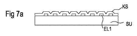
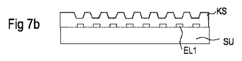
図7aおよび7bは、1つの補償層KSが設けられている1つのSAWデバイスの音響特性が、どのようにしてさらに改善され得るかという可能性を示す。電極と補償層材料との間の小さな音響インピーダンスの差によって低減された電極の反射率は、1つの追加的な、補償層KSのパターニングによってもたらされる反射によって回復される。この目的のため、電極フィンガ(複数)に対し平行して、凹部(複数)(図7a)あるいは隆起部(複数)(図7b)が、補償層KSの表面に取り付けられ、これらは音響波に対する反射部位を生成し、そしてこれらは電極フィンガと同じ走査格子(Raster)に配設され、そしてこれによってこれらの電極フィンガでの反射率が補強される。 7a and 7b show the possibility of how the acoustic properties of one SAW device provided with one compensation layer KS can be further improved. The reflectivity of the electrode reduced by the small acoustic impedance difference between the electrode and the compensation layer material is recovered by the reflection provided by the patterning of one additional compensation layer KS. For this purpose, parallel to the electrode fingers, recesses (FIG. 7a) or ridges (FIG. 7b) are attached to the surface of the compensation layer KS, which are for acoustic waves The reflection sites are created and they are arranged in the same scanning grid (Raster) as the electrode fingers, and this reinforces the reflectivity at these electrode fingers.
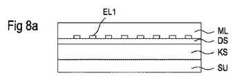
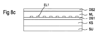
本発明に関しては、圧電結晶/圧電層と電極との間、または補償層の上側での、追加的な誘電体層DSも可能である。図8a〜8cはこのような例示的な実施形態を示す。こうして図8aには、1つの誘電体の層DSが、第1の電極層EL1と補償層KSとの間に配設されている。図8bにおいては、1つの誘電体の層DSが、被覆層MLの上に配設されている。図8cは、2つの誘電体の層DS1およびDS2を同時に備える、1つの実施形態を示す。これらの誘電体の層は既に個別に図8aおよび8bで示されているものである。 In the context of the invention, an additional dielectric layer DS is also possible, between the piezoelectric crystal / piezoelectric layer and the electrode, or above the compensation layer. Figures 8a-8c illustrate such an exemplary embodiment. Thus, in FIG. 8a, one dielectric layer DS is disposed between the first electrode layer EL1 and the compensation layer KS. In FIG. 8b, one dielectric layer DS is arranged on the covering layer ML. FIG. 8c shows one embodiment, which comprises two dielectric layers DS1 and DS2 simultaneously. The layers of these dielectrics are as already shown separately in FIGS. 8a and 8b.
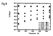
図9は、Sc(1-X)YXF3の系における弾性率Eの温度に依存した変化を、0〜25%のイットリウムの割合に対応した異なるパラメータxに対して示している。20%(x=0.2)のイットリウムの含有量に対して、弾性率Eの最も大きな上昇が300−500Kの温度範囲で生じることが見て取れ、これよりこの材料が弾性率Eの最も大きな正の温度係数を有し、そして音響波で動作するデバイスにおける補償層の使用に最も良く適合している。ここで純粋なフッ化スカンジウムは、負の熱膨張係数を示すが、しかしながら殆ど0に近づくような小さい弾性率Eの温度係数を示す。 FIG. 9 shows the temperature-dependent change of the modulus of elasticity E in the system of Sc (1-X) Y X F 3 for different parameters x corresponding to the proportion of yttrium of 0-25%. It can be seen that for the yttrium content of 20% (x = 0.2), the largest increase of the modulus E occurs in the temperature range of 300-500 K, from which the material has the largest positive E modulus. It has the best temperature coefficient and is best adapted to the use of compensation layers in devices operating with acoustic waves. Here, pure scandium fluoride exhibits a negative coefficient of thermal expansion, but exhibits a temperature coefficient of elastic modulus E which approaches zero.
この図から、あるいはこの元になっている実験から、イットリウムが20〜25%の割合で混合されたスカンジウム−イットリウム−三フッ化物に対し、約1500ppm/Kの中心周波数の温度係数が得られる。これに対しフッ素ドーピングされたSiO2は、700ppm/K未満の係数を示し、一方ドーピングされていないSiO2は、300ppm/K未満の係数を示す。以上により、現在一般的に用いられているドーピングされていないSiO2からなる補償層と比較して、約5倍の補償の改善が得られている。 From this figure, or from the underlying experiment, a temperature coefficient of about 1500 ppm / K center frequency is obtained for scandium-yttrium-trifluoride mixed with yttrium in a proportion of 20 to 25%. In contrast, fluorine-doped SiO 2 exhibits a coefficient of less than 700 ppm / K, while non-doped SiO 2 exhibits a coefficient of less than 300 ppm / K. From the above, an improvement of about 5 times the compensation is obtained as compared with the currently generally used compensation layer composed of undoped SiO 2 .
この材料特性、特に混合されたスカンジウム−イットリウム−三フッ化物の材料特性、たとえば剛性は、従来使用されていたSiO2層と同程度のものとなっている。このSiO2より多少大きな密度では、他のデバイス特性には上記の新しい補償層によって不利な影響を与えられることはないと想定することができる。この改善された補償のために、この補償層の、ほんの小さな層厚が必要なだけであるので、むしろ上記の音響特性の大幅な改善を期待することができる。 The material properties, in particular the material properties of the mixed scandium-yttrium-trifluoride, for example the stiffness, are comparable to those of the conventionally used SiO 2 layers. At densities somewhat greater than this SiO 2 it can be assumed that other device properties are not adversely affected by the new compensation layer described above. Since only a small layer thickness of this compensation layer is necessary for this improved compensation, one can instead expect a significant improvement of the above-mentioned acoustical properties.
本発明は、上記の実施形態例で詳細に説明した実施形態に限定されるものではない。上記の実施形態は、1つの補償層を有する音響波で動作するデバイスの単に例示的な実施形態を示すものである。原理的に、2つ以上の補償層を備えるデバイス、または、中心周波数の温度係数を低減するためのさらなる他の手段、具体的には締め付け層(Verspannungsschichten)を備えるデバイスも可能である。 The invention is not limited to the embodiments described in detail in the example embodiments above. The above embodiments represent merely exemplary embodiments of an acoustic wave operated device having one compensation layer. In principle, a device with more than one compensation layer, or a further means for reducing the temperature coefficient of the center frequency, in particular a device with a clamping layer, is also possible.
Claims (10)
1つの圧電材料の1つの層(SU)と、
前記圧電材料における音響波を励起するための電極(EL,EL1,EL2)の少なくとも1つのペアと、
前記デバイス上に配設されている1つの補償層(KS)であって、当該補償層に音響波のエネルギーの少なくとも一部が存在する、補償層と、
を備え、
前記補償層は、三フッ化スカンジウムScF 3 を含みかつ負の熱膨張係数を有する1つの誘電体材料を含む、
ことを特徴とするデバイス。 A device operating with acoustic waves,
With one layer (SU) of one piezoelectric material,
At least one pair of electrodes (EL, EL1, EL2) for exciting acoustic waves in the piezoelectric material;
A previous SL one compensation layer disposed on the device (KS), at least a portion of the energy of the acoustic wave is present in the compensation layer, and the compensation layer,
Equipped with
The compensation layer comprises one dielectric material comprising scandium trifluoride ScF 3 and having a negative coefficient of thermal expansion ,
A device characterized by
前記補償層(KS)は、前記圧電材料の層上に直接取り付けられており、
前記電極(EL,EL1,EL2)は、前記圧電層(SU)上か、前記補償層(KS)上か、または当該圧電層と当該補償層との間に配設されている、
ことを特徴とするデバイス。 In the device according to claim 1,
The compensation layer (KS) is mounted directly on the layer of piezoelectric material,
The electrodes (EL, EL1, EL2) are disposed on the piezoelectric layer (SU), the compensation layer (KS), or between the piezoelectric layer and the compensation layer.
A device characterized by
SAWデバイスとして構成されており、
少なくとも1つのインターデジタル変換器を、前記圧電層(SU)上に有するか、または前記圧電層(SU)の上方に有し、
前記圧電層および前記インターデジタル変換器の上に堆積された補償層(KS)を有し、当該補償層(KS)は、ScF3を、純粋な形態か、ドーピングされているか、他の酸化物またはハロゲン化物と共に混合結晶となっているか、または結晶質の基質またはガラスの中に埋設されて含み、
前記デバイスの中心周波数での波長に関して、5〜20%の層厚で、前記中心周波数の温度係数が完全に補償されるように形成されている、
ことを特徴とするデバイス。 A device according to any one of claims 1 to 7, said device,
Configured as a SAW device,
At least one interdigital transducer is provided on the piezoelectric layer (SU) or above the piezoelectric layer (SU),
The piezoelectric layer and the compensation layer (KS) deposited on the interdigital transducer, said compensation layer (KS) being in pure form, doped with ScF 3 or other oxide Or mixed with the halide, or embedded in a crystalline substrate or glass,
With a layer thickness of 5 to 20% with respect to the wavelength at the center frequency of the device, the temperature coefficient of the center frequency is formed to be fully compensated .
A device characterized by
1つの圧電材料の1つの層(SU)と、
前記圧電材料における音響波を励起するための電極(EL,EL1,EL2)の少なくとも1つのペアと、
前記デバイス上に配設されている1つの補償層(KS)であって、当該補償層に音響波のエネルギーの少なくとも一部が存在する、補償層と、
を備え、
前記補償層は、負の熱膨張係数を有する1つの誘電体材料を含み、
前記誘電体材料は、以下の化合物Zr(WO 4 )(PO 4 ) 2 ,ScF3−BaF2−YF3,ScF3−BaF2−ZnF2,ScF3−BaF2−InF3,ScF3−MgF2,YbF3−ScF3,LuF3−ScF3,Zn(CN) 2 ,およびゼオライトの1つを含むことを特徴とするデバイス。 A device operating with acoustic waves,
With one layer (SU) of one piezoelectric material,
At least one pair of electrodes (EL, EL1, EL2) for exciting acoustic waves in the piezoelectric material;
One compensation layer (KS) disposed on the device, wherein at least a portion of the energy of the acoustic wave is present in the compensation layer;
Equipped with
The compensation layer comprises one dielectric material having a negative coefficient of thermal expansion,
The dielectric material, the following compounds Zr (WO 4) (PO 4 ) 2, ScF 3 -BaF 2 -YF 3, ScF 3 -BaF 2 -ZnF 2, ScF 3 -BaF 2 -InF 3, ScF 3 - MgF 2, YbF 3 -ScF 3, LuF 3 -ScF 3 device, characterized in that it comprises, Zn (CN) 2, and one of the zeolites.
Applications Claiming Priority (3)
| Application Number | Priority Date | Filing Date | Title |
|---|---|---|---|
| DE102014111993.2 | 2014-08-21 | ||
| DE102014111993.2A DE102014111993B4 (en) | 2014-08-21 | 2014-08-21 | Microacoustic device with improved temperature compensation |
| PCT/EP2015/065728 WO2016026612A1 (en) | 2014-08-21 | 2015-07-09 | Micro-acoustic component having improved temperature compensation |
Publications (2)
| Publication Number | Publication Date |
|---|---|
| JP2017523645A JP2017523645A (en) | 2017-08-17 |
| JP6517841B2 true JP6517841B2 (en) | 2019-05-22 |
Family
ID=53539724
Family Applications (1)
| Application Number | Title | Priority Date | Filing Date |
|---|---|---|---|
| JP2016570834A Expired - Fee Related JP6517841B2 (en) | 2014-08-21 | 2015-07-09 | Micro-acoustic device with improved temperature compensation |
Country Status (6)
| Country | Link |
|---|---|
| US (1) | US10224897B2 (en) |
| EP (1) | EP3183811A1 (en) |
| JP (1) | JP6517841B2 (en) |
| CN (1) | CN106716826B (en) |
| DE (1) | DE102014111993B4 (en) |
| WO (1) | WO2016026612A1 (en) |
Families Citing this family (10)
| Publication number | Priority date | Publication date | Assignee | Title |
|---|---|---|---|---|
| CN107060592B (en) * | 2016-12-21 | 2018-05-25 | 重庆金华兴门业有限公司 | Extension spring-type inside contracts door |
| CN107871813B (en) * | 2017-11-17 | 2020-08-11 | 中国电子科技集团公司第二十六研究所 | Temperature compensation layer planarization method of temperature compensation type surface acoustic wave device |
| TW201930192A (en) * | 2017-12-01 | 2019-08-01 | 美商天工方案公司 | Alternative temperature compensating materials to amorphous silica in acoustic wave resonators |
| CN108866677A (en) * | 2018-07-05 | 2018-11-23 | 合肥萃励新材料科技有限公司 | A kind of ZrW2O8The preparation method of sub-micron fibers |
| WO2020132999A1 (en) * | 2018-12-26 | 2020-07-02 | 天津大学 | Resonator with temperature compensation layer, and filter |
| WO2022224740A1 (en) * | 2021-04-22 | 2022-10-27 | 株式会社村田製作所 | Ladder-type filter |
| JPWO2023021777A1 (en) * | 2021-08-19 | 2023-02-23 | ||
| CN114531130B (en) * | 2022-02-23 | 2025-08-29 | 广东广纳芯科技有限公司 | Temperature Compensated Resonator |
| CN115733459A (en) * | 2022-11-25 | 2023-03-03 | 常州承芯半导体有限公司 | Surface acoustic wave resonance device, forming method thereof and surface acoustic wave filter device |
| CN117833855B (en) * | 2024-03-04 | 2024-10-15 | 深圳新声半导体有限公司 | Sound wave device |
Family Cites Families (16)
| Publication number | Priority date | Publication date | Assignee | Title |
|---|---|---|---|---|
| US3965444A (en) * | 1975-01-03 | 1976-06-22 | Raytheon Company | Temperature compensated surface acoustic wave devices |
| JPH08181562A (en) * | 1994-12-21 | 1996-07-12 | Meidensha Corp | Surface acoustic wave element |
| JP2000196410A (en) * | 1998-12-31 | 2000-07-14 | Kazuhiko Yamanouchi | High-stability and high-coupling surface acoustic wave substrate, surface acoustic wave filter using the same and surface acoustic wave function element |
| US7332985B2 (en) | 2003-10-30 | 2008-02-19 | Avago Technologies Wireless Ip (Singapore) Pte Ltd. | Cavity-less film bulk acoustic resonator (FBAR) devices |
| US7362198B2 (en) * | 2003-10-30 | 2008-04-22 | Avago Technologies Wireless Ip (Singapore) Pte. Ltd | Pass bandwidth control in decoupled stacked bulk acoustic resonator devices |
| US7019605B2 (en) * | 2003-10-30 | 2006-03-28 | Larson Iii John D | Stacked bulk acoustic resonator band-pass filter with controllable pass bandwidth |
| JP2006033748A (en) * | 2004-07-21 | 2006-02-02 | Matsushita Electric Ind Co Ltd | Thin film bulk acoustic wave resonator |
| DE102004045181B4 (en) | 2004-09-17 | 2016-02-04 | Epcos Ag | SAW device with reduced temperature response and method of manufacture |
| JP5039362B2 (en) | 2006-11-07 | 2012-10-03 | 太陽誘電株式会社 | Elastic wave device |
| JP5190841B2 (en) * | 2007-05-31 | 2013-04-24 | 独立行政法人産業技術総合研究所 | Piezoelectric thin film, piezoelectric body and manufacturing method thereof, and piezoelectric resonator, actuator element, and physical sensor using the piezoelectric thin film |
| JP2008125130A (en) | 2008-02-08 | 2008-05-29 | Murata Mfg Co Ltd | Surface acoustic wave device and its manufacturing method |
| JP2014027639A (en) | 2012-07-24 | 2014-02-06 | Kazuhiko Yamanouchi | Temperature ultrahigh stability thin film structure pseudo surface acoustic wave substrate and surface acoustic wave function element employing the substrate |
| CN102904546B (en) * | 2012-08-30 | 2016-04-13 | 中兴通讯股份有限公司 | The adjustable piezoelectric acoustic wave resonator of a kind of temperature compensation capability |
| CN103684336B (en) * | 2012-08-31 | 2017-01-11 | 安华高科技通用Ip(新加坡)公司 | Resonator device with electrode comprising embedded type temperature compensation layer |
| DE102012111889B9 (en) | 2012-12-06 | 2014-09-04 | Epcos Ag | Electroacoustic transducer |
| US9401691B2 (en) * | 2014-04-30 | 2016-07-26 | Avago Technologies General Ip (Singapore) Pte. Ltd. | Acoustic resonator device with air-ring and temperature compensating layer |
-
2014
- 2014-08-21 DE DE102014111993.2A patent/DE102014111993B4/en not_active Expired - Fee Related
-
2015
- 2015-07-09 WO PCT/EP2015/065728 patent/WO2016026612A1/en not_active Ceased
- 2015-07-09 EP EP15735958.9A patent/EP3183811A1/en not_active Withdrawn
- 2015-07-09 CN CN201580050878.9A patent/CN106716826B/en active Active
- 2015-07-09 JP JP2016570834A patent/JP6517841B2/en not_active Expired - Fee Related
- 2015-07-09 US US15/314,790 patent/US10224897B2/en active Active
Also Published As
| Publication number | Publication date |
|---|---|
| EP3183811A1 (en) | 2017-06-28 |
| US20170194932A1 (en) | 2017-07-06 |
| JP2017523645A (en) | 2017-08-17 |
| DE102014111993A1 (en) | 2016-02-25 |
| WO2016026612A1 (en) | 2016-02-25 |
| US10224897B2 (en) | 2019-03-05 |
| DE102014111993B4 (en) | 2017-12-21 |
| CN106716826B (en) | 2020-09-29 |
| CN106716826A (en) | 2017-05-24 |
Similar Documents
| Publication | Publication Date | Title |
|---|---|---|
| JP6517841B2 (en) | Micro-acoustic device with improved temperature compensation | |
| US12445105B2 (en) | Elastic wave device and method for manufacturing the same | |
| US9553561B2 (en) | Vibrating device and manufacturing method therfor | |
| JP5161698B2 (en) | Piezoelectric thin film resonator and filter or duplexer using the same | |
| US9425764B2 (en) | Accoustic resonator having composite electrodes with integrated lateral features | |
| JP5994850B2 (en) | Bulk wave resonator | |
| US9444426B2 (en) | Accoustic resonator having integrated lateral feature and temperature compensation feature | |
| US8629598B2 (en) | Boundary acoustic wave device | |
| KR20190077224A (en) | Elastic wave device | |
| SG11202110974YA (en) | High-order mode surface acoustic wave device | |
| WO2006114930A1 (en) | Boundary acoustic wave device | |
| KR20170128505A (en) | Seismic wave device | |
| JP5687776B2 (en) | Acoustic wave operating member and manufacturing method thereof | |
| CN110868182B (en) | Resonators and Filters | |
| JP7120441B2 (en) | Acoustic wave device | |
| JP2017509246A (en) | BAW resonator with temperature compensation unit | |
| WO2013172287A1 (en) | Acoustic wave device | |
| KR102310917B1 (en) | Elastic wave device | |
| WO2020069805A1 (en) | Electroacoustic resonator with several transversal wave velocity portions | |
| JP2009100367A (en) | Piezoelectric vibration device | |
| JPWO2010100967A1 (en) | Surface acoustic wave device | |
| KR100956244B1 (en) | Piezoelectric vibrator and electrode structure of piezoelectric vibrator | |
| CN119341506B (en) | Elastic wave resonator and its communication device | |
| JP5589403B2 (en) | Piezoelectric resonator | |
| JP2002009579A (en) | Piezo electric resonator and piezoelectric filter using the same |
Legal Events
| Date | Code | Title | Description |
|---|---|---|---|
| A621 | Written request for application examination |
Free format text: JAPANESE INTERMEDIATE CODE: A621 Effective date: 20170125 |
|
| A711 | Notification of change in applicant |
Free format text: JAPANESE INTERMEDIATE CODE: A711 Effective date: 20170620 |
|
| A131 | Notification of reasons for refusal |
Free format text: JAPANESE INTERMEDIATE CODE: A131 Effective date: 20180411 |
|
| A521 | Request for written amendment filed |
Free format text: JAPANESE INTERMEDIATE CODE: A523 Effective date: 20180706 |
|
| A131 | Notification of reasons for refusal |
Free format text: JAPANESE INTERMEDIATE CODE: A131 Effective date: 20180912 |
|
| A521 | Request for written amendment filed |
Free format text: JAPANESE INTERMEDIATE CODE: A523 Effective date: 20181207 |
|
| TRDD | Decision of grant or rejection written | ||
| A01 | Written decision to grant a patent or to grant a registration (utility model) |
Free format text: JAPANESE INTERMEDIATE CODE: A01 Effective date: 20190327 |
|
| A61 | First payment of annual fees (during grant procedure) |
Free format text: JAPANESE INTERMEDIATE CODE: A61 Effective date: 20190418 |
|
| R150 | Certificate of patent or registration of utility model |
Ref document number: 6517841 Country of ref document: JP Free format text: JAPANESE INTERMEDIATE CODE: R150 |
|
| LAPS | Cancellation because of no payment of annual fees |