JP6513478B2 - Antenna module and mobile terminal using the same - Google Patents
Antenna module and mobile terminal using the same Download PDFInfo
- Publication number
- JP6513478B2 JP6513478B2 JP2015103472A JP2015103472A JP6513478B2 JP 6513478 B2 JP6513478 B2 JP 6513478B2 JP 2015103472 A JP2015103472 A JP 2015103472A JP 2015103472 A JP2015103472 A JP 2015103472A JP 6513478 B2 JP6513478 B2 JP 6513478B2
- Authority
- JP
- Japan
- Prior art keywords
- conductive member
- antenna module
- connection member
- conductive
- mobile terminal
- Prior art date
- Legal status (The legal status is an assumption and is not a legal conclusion. Google has not performed a legal analysis and makes no representation as to the accuracy of the status listed.)
- Expired - Fee Related
Links
Images


Classifications
-
- H—ELECTRICITY
- H01—ELECTRIC ELEMENTS
- H01Q—ANTENNAS, i.e. RADIO AERIALS
- H01Q1/00—Details of, or arrangements associated with, antennas
- H01Q1/12—Supports; Mounting means
- H01Q1/22—Supports; Mounting means by structural association with other equipment or articles
- H01Q1/24—Supports; Mounting means by structural association with other equipment or articles with receiving set
- H01Q1/241—Supports; Mounting means by structural association with other equipment or articles with receiving set used in mobile communications, e.g. GSM
- H01Q1/242—Supports; Mounting means by structural association with other equipment or articles with receiving set used in mobile communications, e.g. GSM specially adapted for hand-held use
- H01Q1/243—Supports; Mounting means by structural association with other equipment or articles with receiving set used in mobile communications, e.g. GSM specially adapted for hand-held use with built-in antennas
-
- H—ELECTRICITY
- H01—ELECTRIC ELEMENTS
- H01Q—ANTENNAS, i.e. RADIO AERIALS
- H01Q1/00—Details of, or arrangements associated with, antennas
- H01Q1/36—Structural form of radiating elements, e.g. cone, spiral, umbrella; Particular materials used therewith
- H01Q1/38—Structural form of radiating elements, e.g. cone, spiral, umbrella; Particular materials used therewith formed by a conductive layer on an insulating support
-
- H—ELECTRICITY
- H01—ELECTRIC ELEMENTS
- H01Q—ANTENNAS, i.e. RADIO AERIALS
- H01Q1/00—Details of, or arrangements associated with, antennas
- H01Q1/48—Earthing means; Earth screens; Counterpoises
-
- H—ELECTRICITY
- H01—ELECTRIC ELEMENTS
- H01Q—ANTENNAS, i.e. RADIO AERIALS
- H01Q1/00—Details of, or arrangements associated with, antennas
- H01Q1/50—Structural association of antennas with earthing switches, lead-in devices or lightning protectors
-
- H—ELECTRICITY
- H01—ELECTRIC ELEMENTS
- H01Q—ANTENNAS, i.e. RADIO AERIALS
- H01Q1/00—Details of, or arrangements associated with, antennas
- H01Q1/52—Means for reducing coupling between antennas; Means for reducing coupling between an antenna and another structure
-
- H—ELECTRICITY
- H01—ELECTRIC ELEMENTS
- H01Q—ANTENNAS, i.e. RADIO AERIALS
- H01Q5/00—Arrangements for simultaneous operation of antennas on two or more different wavebands, e.g. dual-band or multi-band arrangements
- H01Q5/30—Arrangements for providing operation on different wavebands
-
- H—ELECTRICITY
- H01—ELECTRIC ELEMENTS
- H01Q—ANTENNAS, i.e. RADIO AERIALS
- H01Q5/00—Arrangements for simultaneous operation of antennas on two or more different wavebands, e.g. dual-band or multi-band arrangements
- H01Q5/30—Arrangements for providing operation on different wavebands
- H01Q5/307—Individual or coupled radiating elements, each element being fed in an unspecified way
- H01Q5/314—Individual or coupled radiating elements, each element being fed in an unspecified way using frequency dependent circuits or components, e.g. trap circuits or capacitors
- H01Q5/335—Individual or coupled radiating elements, each element being fed in an unspecified way using frequency dependent circuits or components, e.g. trap circuits or capacitors at the feed, e.g. for impedance matching
-
- H—ELECTRICITY
- H01—ELECTRIC ELEMENTS
- H01Q—ANTENNAS, i.e. RADIO AERIALS
- H01Q7/00—Loop antennas with a substantially uniform current distribution around the loop and having a directional radiation pattern in a plane perpendicular to the plane of the loop
-
- H—ELECTRICITY
- H01—ELECTRIC ELEMENTS
- H01Q—ANTENNAS, i.e. RADIO AERIALS
- H01Q9/00—Electrically-short antennas having dimensions not more than twice the operating wavelength and consisting of conductive active radiating elements
- H01Q9/04—Resonant antennas
- H01Q9/16—Resonant antennas with feed intermediate between the extremities of the antenna, e.g. centre-fed dipole
- H01Q9/26—Resonant antennas with feed intermediate between the extremities of the antenna, e.g. centre-fed dipole with folded element or elements, the folded parts being spaced apart a small fraction of operating wavelength
Description
本発明は、無線信号を送受信するアンテナモジュールを備える移動端末機に関する。 The present invention relates to a mobile terminal provided with an antenna module for transmitting and receiving radio signals.
端末機は、移動可能であるか否かによって、移動端末機(mobile/portable terminal)と固定端末機(stationary terminal)に分けられる。さらに、移動端末機は、ユーザが直接携帯可能であるか否かによって、携帯(型)端末機(handheld terminal)と車載端末機(vehicle mount terminal)に分けられる。 The terminal is divided into a mobile terminal (mobile / portable terminal) and a stationary terminal according to whether it is movable or not. In addition, the mobile terminal can be divided into a handheld terminal and a vehicle mount terminal depending on whether the user can directly carry the mobile terminal.
移動端末機の機能は多様化している。例えば、データ通信及び音声通信、カメラによる写真撮影及び動画像撮影、音声録音、スピーカシステムによる音楽ファイルの再生、ディスプレイ部への静止画像及び動画像の出力などの機能がある。一部の移動端末機は、電子ゲーム機能やマルチメディアプレーヤ機能を備える。特に、最近の移動端末機は、放送、ビデオ、テレビ番組などの視覚的コンテンツを提供するマルチキャスト信号を受信することができる。 Mobile terminal functions are diversifying. For example, there are functions such as data communication and voice communication, photography and moving picture shooting with a camera, voice recording, reproduction of a music file by a speaker system, and output of a still image and a moving image to a display unit. Some mobile terminals have an electronic game function and a multimedia player function. In particular, modern mobile terminals can receive multicast signals providing visual content such as broadcasts, videos, television programs and the like.
このような端末機は、機能が多様化することにより、例えば写真や動画像の撮影、音楽や動画像ファイルの再生、ゲーム、放送受信などの複合的な機能を備えたマルチメディア機器の形で実現されている。 Such terminals are, for example, in the form of multimedia equipment having complex functions such as photographing of pictures and moving pictures, reproduction of music and moving picture files, games, broadcast reception, etc. by diversification of functions. It has been realized.
このような端末機の機能をサポート及び向上させるために、端末機の構造的な部分及び/又はソフトウェア的な部分の改良が試みられている。 In order to support and improve the functions of such terminals, improvements in structural and / or software parts of the terminals have been attempted.
アンテナは、無線通信のために無線電磁波を送受信するように構成される装置であり、移動端末機の必須構成要素である。移動端末機が音声通話の他にLTE、DMBなどの様々な機能を実現するようになっているので、アンテナは、前記機能を満たす帯域幅を実現しなければならないだけでなく、移動端末機に内蔵できるように小型に設計されなければならない。 An antenna is an apparatus configured to transmit and receive wireless electromagnetic waves for wireless communication, and is an essential component of a mobile terminal. Since the mobile terminal is to realize various functions such as LTE, DMB, etc. in addition to the voice call, the antenna must not only realize the bandwidth satisfying the function but also to the mobile terminal. It must be designed to be small enough to be built-in.
移動端末機に一般的に用いられる板状逆Fアンテナ(PIFA)は、帯域幅が狭いので、多重帯域、広帯域のアンテナ特性の実現が困難であるという問題があった。このような問題を解決するために、多重帯域を実現できるようにする構造的な改良が行われている。 A planar inverted F antenna (PIFA) generally used for mobile terminals has a narrow bandwidth, which makes it difficult to realize multiband and wideband antenna characteristics. In order to solve such problems, structural improvements have been made to enable multiple bands to be realized.
また、移動端末機のベゼルが次第に細くなっているので、アンテナの配置空間も次第に狭くなっている。このような状況を反映して、近年、移動端末機の外観を形成する金属部材をアンテナとして活用する移動端末機が市場に投入されている。 In addition, since the bezel of the mobile terminal is gradually narrowed, the space for arranging the antenna is also narrowed gradually. In light of this situation, mobile terminals that use a metal member forming the appearance of the mobile terminal as an antenna have recently been introduced into the market.
本発明の目的は、上記問題及び他の問題を解決することにある。 It is an object of the present invention to solve the above problems and other problems.
本発明の他の目的は、広帯域特性が得られるアンテナモジュールを備える移動端末機を提供することにある。 Another object of the present invention is to provide a mobile terminal equipped with an antenna module capable of obtaining wide band characteristics.
本発明のさらに他の目的は、移動端末機の外観を形成する金属部材自体をアンテナとして用いる新しい構造の移動端末機を提供することにある。 Another object of the present invention is to provide a mobile terminal having a new structure using as an antenna a metal member that forms the appearance of the mobile terminal.
上記目的又は他の目的を達成するために、本発明の一実施形態によるアンテナモジュールは、給電部及び接地部に接続される第1導電部材と、前記第1導電部材から離隔して配置される第2導電部材と、前記給電部に近い位置で前記第1導電部材と前記第2導電部材とを接続する第1接続部材と、前記接地部に近い位置で前記第1導電部材と前記第2導電部材とを接続する第2接続部材とを含み、前記第1導電部材にはスリットが形成され、前記スリットは前記給電部と前記接地部との間に形成される。 In order to achieve the above object or another object, the antenna module according to one embodiment of the present invention is disposed apart from the first conductive member connected to the feeding portion and the grounding portion, and the first conductive member. A second conductive member, a first connecting member connecting the first conductive member and the second conductive member at a position close to the feeding portion, and a first conductive member and the second connecting member at a position near the ground portion. And a second connecting member connected to the conductive member, wherein the first conductive member is formed with a slit, and the slit is formed between the feeding portion and the ground portion.
本発明の一態様によれば、前記第1導電部材のうち前記第1接続部材が接続される部分の位置は、前記給電部が接続される部分と前記第1導電部材の端部との間で可変であってもよい。 According to one aspect of the present invention, the position of the portion of the first conductive member to which the first connection member is connected is between the portion to which the power feeding unit is connected and the end of the first conductive member And may be variable.
本発明の一態様によれば、前記第1導電部材のうち前記第2接続部材が接続される部分の位置は、前記接地部が接続される部分と前記第1導電部材の端部との間で可変であってもよい。 According to one aspect of the present invention, the position of the portion of the first conductive member to which the second connection member is connected is between the portion to which the ground portion is connected and the end of the first conductive member And may be variable.
本発明の一態様によれば、前記アンテナモジュールは、一端部が前記第1導電部材に接続され、他端部が前記第2導電部材に接続される第3接続部材をさらに含み、前記第1導電部材のうち前記第3接続部材が接続される部分の位置は、前記接地部が接続される部分と前記第2接続部材が接続される部分との間で可変であり、前記第2導電部材のうち前記第3接続部材が接続される部分の位置は、前記第1接続部材が接続される部分と前記第2接続部材が接続される部分との間で可変であってもよい。 According to one aspect of the present invention, the antenna module further includes a third connecting member having one end connected to the first conductive member and the other end connected to the second conductive member, The position of the portion of the conductive member to which the third connection member is connected is variable between the portion to which the ground portion is connected and the portion to which the second connection member is connected, and the second conductive member The position of the portion to which the third connection member is connected may be variable between the portion to which the first connection member is connected and the portion to which the second connection member is connected.
本発明の一態様によれば、前記アンテナモジュールは、一端部が前記第1導電部材もしくは前記第2導電部材に接続されるか又はグランドに接地され、他端部が開放されるサブアームをさらに含み、前記サブアームの一端部が前記第1導電部材に接続される場合、前記一端部は前記接地部が接続される部分と前記第3接続部材が接続される部分との間に形成され、前記サブアームの一端部が前記第2導電部材に接続される場合、前記一端部は前記第1接続部材が接続される部分と前記第3接続部材が接続される部分との間に形成され、前記サブアームの一端部が前記グランドに接地される場合、前記他端部の少なくとも一部は前記第2導電部材の近傍に離隔形成されるようにしてもよい。 According to one aspect of the present invention, the antenna module further includes a sub arm having one end connected to the first conductive member or the second conductive member or grounded to the ground, and the other end opened. When one end of the sub arm is connected to the first conductive member, the one end is formed between a portion to which the ground portion is connected and a portion to which the third connection member is connected, the sub arm When one end portion of the sub-arm is connected to the second conductive member, the one end portion is formed between a portion to which the first connection member is connected and a portion to which the third connection member is connected, and When one end portion is grounded to the ground, at least a portion of the other end portion may be formed separately in the vicinity of the second conductive member.
本発明の一態様によれば、前記第1導電部材は、前記接地部が接続される第1部分と、前記第1部分から所定間隔離隔して前記スリットを形成し、前記給電部が接続される第2部分とを含んでもよい。 According to one aspect of the present invention, the first conductive member forms the slit separated from the first portion by a predetermined distance from the first portion to which the ground portion is connected, and the feed portion is connected. And a second part.
本発明の一態様によれば、前記第1導電部材に給電するように前記給電部に接続される給電ラインには、インピーダンスマッチングのための第1マッチングモジュールが配置されてもよい。 According to an aspect of the present invention, a first matching module for impedance matching may be disposed on a feed line connected to the feed section to feed the first conductive member.
本発明の一態様によれば、前記第1マッチングモジュールには、前記第2部分に流れる電流を制御する第1可変スイッチが接続されてもよい。 According to one aspect of the present invention, the first matching module may be connected to a first variable switch that controls the current flowing through the second portion.
本発明の一態様によれば、前記第1導電部材を接地するように前記接地部に接続される接地ラインには、インピーダンスマッチングのための第2マッチングモジュールが配置されてもよい。 According to an aspect of the present invention, a second matching module for impedance matching may be disposed on a ground line connected to the ground portion to ground the first conductive member.
本発明の一態様によれば、前記第2マッチングモジュールには、前記第1部分に流れる電流を制御する第2可変スイッチが接続されてもよい。 According to one aspect of the present invention, the second matching module may be connected to a second variable switch that controls the current flowing to the first portion.
本発明の一態様によれば、前記サブアームには、前記サブアームに流れる電流を制御する第3可変スイッチが接続されてもよい。 According to an aspect of the present invention, a third variable switch that controls a current flowing to the sub arm may be connected to the sub arm.
本発明の他の実施形態によるアンテナモジュールは、第1給電部により給電される第1導電部材と、前記第1導電部材から離隔して配置され、第2給電部により給電される第2導電部材と、前記第1給電部に近い位置で前記第1導電部材と前記第2導電部材とを接続する第1接続部材と、一端部が前記第1導電部材に接続され、他端部が前記第2導電部材に接続される第2接続部材とを含み、前記第2接続部材の一端部の位置は、前記第1給電部が接続される部分と前記第1導電部材の端部との間で可変であり、前記第2接続部材の他端部の位置は、前記第2給電部が接続される部分と前記第2導電部材の端部との間で可変であり、前記第1導電部材及び前記第2導電部材は、前記第2給電部に近い位置で開放されている。 An antenna module according to another embodiment of the present invention includes a first conductive member fed by a first feeding portion, and a second conductive member spaced from the first conductive member and fed by a second feeding portion. And a first connection member connecting the first conductive member and the second conductive member at a position close to the first power feeding portion, one end portion is connected to the first conductive member, and the other end portion is A second connection member connected to the second conductive member, the position of the one end of the second connection member being between the portion to which the first power feeding portion is connected and the end of the first conductive member The position of the other end of the second connection member is variable between the portion to which the second power feeding portion is connected and the end of the second conductive member, and the first conductive member and The second conductive member is open at a position close to the second feeding portion.
本発明の一態様によれば、前記アンテナモジュールは、前記第2導電部材に形成され、一端部が前記第2給電部が接続される部分と前記第2導電部材の開放端との間に形成され、他端部が開放されるサブアームをさらに含んでもよい。 According to one aspect of the present invention, the antenna module is formed on the second conductive member, and one end thereof is formed between a portion to which the second feeding portion is connected and an open end of the second conductive member. And may further include a sub arm whose other end is opened.
本発明の一態様によれば、前記アンテナモジュールは、前記第2導電部材のうち前記第2接続部材が接続される部分と前記第2給電部が接続される部分との間に形成され、前記第2給電部から発生して前記第1給電部に流れる電流を遮断する第1ブロック部材をさらに含んでもよい。 According to one aspect of the present invention, the antenna module is formed between a portion of the second conductive member to which the second connection member is connected and a portion to which the second feeding portion is connected, It may further include a first block member that interrupts the current generated from the second power supply unit and flowing to the first power supply unit.
本発明の一態様によれば、前記アンテナモジュールは、前記第2導電部材に給電するように前記第2給電部に接続される第2給電ラインに形成され、前記第1給電部から発生して前記第2給電部に流れる電流を遮断する第2ブロック部材をさらに含んでもよい。 According to one aspect of the present invention, the antenna module is formed on a second feed line connected to the second feed section so as to feed the second conductive member, and is generated from the first feed section. It may further include a second block member for interrupting the current flowing to the second power supply unit.
本発明の一態様によれば、前記第1導電部材は、接地ラインを介してグランドに接地され、前記接地ラインには、第2可変スイッチが接続されてもよい。 According to one aspect of the present invention, the first conductive member may be grounded to a ground via a ground line, and a second variable switch may be connected to the ground line.
本発明の一態様によれば、前記第1導電部材に給電する第1給電ラインには、第1マッチングモジュールが配置されてもよい。 According to an aspect of the present invention, a first matching module may be disposed on a first feed line feeding the first conductive member.
本発明の一態様によれば、前記第1マッチングモジュールには、前記第1導電部材に流れる電流を制御する第1可変スイッチが接続されてもよい。 According to one aspect of the present invention, the first matching module may be connected to a first variable switch that controls a current flowing to the first conductive member.
本発明の一態様によれば、前記第1ブロック部材及び前記第2ブロック部材は、集中定数素子を含んでもよい。 According to one aspect of the present invention, the first block member and the second block member may include lumped constant elements.
本発明の一態様によれば、前記第1導電部材との電気的結合(electric coupling)を生じさせるように、前記サブアームの少なくとも一部は前記第1導電部材の近傍に離隔形成されてもよい。 According to one aspect of the present invention, at least a portion of the sub-arms may be spaced apart near the first conductive member so as to cause an electrical coupling with the first conductive member. .
本発明のさらに他の実施形態による移動端末機は、端末機本体と、前記端末機本体に形成されるアンテナモジュールとを含み、前記アンテナモジュールは、互いに離隔して配置される第1導電部材及び第2導電部材と、前記第1導電部材及び前記第2導電部材の両端をそれぞれ接続する第1接続部材及び第2接続部材と、一端部が前記第2導電部材に接続され、他端部が前記第1導電部材に接続される第3接続部材とを含み、前記第1導電部材は給電部及び接地部に接続され、前記第1導電部材又は前記第2導電部材にはスリットが形成され、前記スリットは前記給電部と前記接地部との間に形成され、前記第1導電部材のうち前記第3接続部材が接続される部分の位置は、前記接地部が接続される部分と前記第2接続部材が接続される部分との間で可変であり、前記第2導電部材のうち前記第3接続部材が接続される部分の位置は、前記第1接続部材が接続される部分と前記第2接続部材が接続される部分との間で可変であってもよい。 A mobile terminal according to still another embodiment of the present invention includes a terminal body and an antenna module formed in the terminal body, the antenna module comprising a first conductive member disposed apart from each other, and A second conductive member, a first connecting member and a second connecting member respectively connecting both ends of the first conductive member and the second conductive member, one end portion is connected to the second conductive member, and the other end portion is And a third connection member connected to the first conductive member, wherein the first conductive member is connected to a power feeding portion and a ground portion, and a slit is formed in the first conductive member or the second conductive member. The slit is formed between the feeding portion and the ground portion, and the position of the portion of the first conductive member to which the third connection member is connected is the portion to which the ground portion is connected and the second portion. Part to which connecting member is connected The position of the portion of the second conductive member to which the third connection member is connected is the portion to which the first connection member is connected and the portion to which the second connection member is connected. It may be variable between
本発明の一態様によれば、前記第1導電部材及び前記第2導電部材は、いずれか一方が前記端末機本体の側面外観の一部又は全部を形成し、他方が前記端末機本体の内部に配置されるようにしてもよい。 According to one aspect of the present invention, one of the first conductive member and the second conductive member forms a part or all of the side appearance of the terminal body, and the other is an inner portion of the terminal body It may be arranged in
本発明の一態様によれば、前記第1導電部材及び前記第2導電部材は、平面からなり、前記各平面が互いに垂直に形成されるようにしてもよい。 According to one aspect of the present invention, the first conductive member and the second conductive member may be flat surfaces, and the flat surfaces may be formed to be perpendicular to each other.
本発明の一態様によれば、前記第2導電部材は、不均一なパターンに形成されてもよい。 According to one aspect of the present invention, the second conductive member may be formed in a non-uniform pattern.
本発明の一態様によれば、前記第1導電部材のうち前記第1接続部材が接続される部分の位置は、前記給電部が接続される部分と前記第1導電部材の端部との間で可変であってもよい。 According to one aspect of the present invention, the position of the portion of the first conductive member to which the first connection member is connected is between the portion to which the power feeding unit is connected and the end of the first conductive member And may be variable.
本発明の一態様によれば、前記第1導電部材のうち前記第2接続部材が接続される部分の位置は、前記接地部が接続される部分と前記第1導電部材の端部との間で可変であってもよい。 According to one aspect of the present invention, the position of the portion of the first conductive member to which the second connection member is connected is between the portion to which the ground portion is connected and the end of the first conductive member And may be variable.
本発明の一態様によれば、前記アンテナモジュールは、一端部が前記第1導電部材に接続され、他端部が開放されるサブアームをさらに含み、前記サブアームの一端部は前記接地部が接続される部分と前記第3接続部材が接続される部分との間に形成されてもよい。 According to one aspect of the present invention, the antenna module further includes a sub arm whose one end is connected to the first conductive member and whose other end is open, and one end of the sub arm is connected to the ground portion. The third connection member may be formed between the first portion and the second portion.
本発明のさらに他の実施形態による移動端末機は、端末機本体と、前記端末機本体に形成されるアンテナモジュールとを含み、前記アンテナモジュールは、互いに離隔して配置され、第1給電部及び第2給電部によりそれぞれ給電される第1導電部材及び第2導電部材と、前記第1給電部に近い位置で前記第1導電部材と前記第2導電部材とを接続する第1接続部材と、一端部が前記第1導電部材に接続され、他端部が前記第2導電部材に接続される第2接続部材とを含み、前記第2接続部材の一端部の位置は、前記第1給電部が接続される部分と前記第1導電部材の端部との間で可変であり、前記第2接続部材の他端部の位置は、前記第2給電部が接続される部分と前記第2導電部材の端部との間で可変であり、前記第1導電部材及び前記第2導電部材は、前記第2給電部に近い位置で開放されている。 A mobile terminal according to another embodiment of the present invention includes a terminal body and an antenna module formed in the terminal body, wherein the antenna modules are spaced apart from each other, and the first power feeding unit and A first conductive member and a second conductive member respectively fed by a second feeding portion; and a first connection member connecting the first conductive member and the second conductive member at a position close to the first feeding portion; And a second connection member whose one end is connected to the first conductive member and the other end is connected to the second conductive member, and the position of the one end of the second connection member is the first power feeder Is variable between the portion to which the second connection member is connected and the end of the first conductive member, and the position of the other end of the second connection member is the portion to which the second feeding portion is connected and the second conductive member. Variable between the end of the member and the first conductive member; Second conductive member is open at a position closer to the second power source.
本発明の一態様によれば、前記第1導電部材及び前記第2導電部材は、いずれか一方が前記端末機本体の側面外観の一部又は全部を形成し、他方が前記端末機本体の内部に配置されるようにしてもよい。 According to one aspect of the present invention, one of the first conductive member and the second conductive member forms a part or all of the side appearance of the terminal body, and the other is an inner portion of the terminal body It may be arranged in
本発明の一態様によれば、前記アンテナモジュールは、前記第2導電部材のうち前記第2接続部材が接続される部分と前記第2給電部が接続される部分との間に形成され、前記第2給電部から発生して前記第1給電部に流れる電流を遮断する第1ブロック部材をさらに含んでもよい。 According to one aspect of the present invention, the antenna module is formed between a portion of the second conductive member to which the second connection member is connected and a portion to which the second feeding portion is connected, It may further include a first block member that interrupts the current generated from the second power supply unit and flowing to the first power supply unit.
本発明の一態様によれば、前記アンテナモジュールは、前記第2導電部材に給電するように前記第2給電部に接続される第2給電ラインに形成され、前記第1給電部から発生して前記第2給電部に流れる電流を遮断する第2ブロック部材をさらに含んでもよい。 According to one aspect of the present invention, the antenna module is formed on a second feed line connected to the second feed section so as to feed the second conductive member, and is generated from the first feed section. It may further include a second block member for interrupting the current flowing to the second power supply unit.
本発明の一態様によれば、前記アンテナモジュールは、前記第2導電部材に形成され、一端部が前記第2給電部が接続される部分と前記第2導電部材の開放端との間に形成され、他端部が開放されるサブアームをさらに含んでもよい。 According to one aspect of the present invention, the antenna module is formed on the second conductive member, and one end thereof is formed between a portion to which the second feeding portion is connected and an open end of the second conductive member. And may further include a sub arm whose other end is opened.
本発明の適用範囲は以下の発明の詳細な説明から明らかになるであろう。しかし、以下の発明の詳細な説明及び特定の実施形態は単に例示にすぎず、当業者であれば本発明の思想や範囲内で様々な変更及び修正が可能であることを理解できるであろう。 The scope of application of the present invention will be apparent from the detailed description of the invention below. However, the following detailed description of the invention and the specific embodiments are merely exemplary, and it will be understood by those skilled in the art that various changes and modifications can be made within the spirit and scope of the present invention. .
本発明によるアンテナモジュール及びそれを用いた移動端末機の効果は次の通りである。 The effects of the antenna module according to the present invention and the mobile terminal using the same are as follows.
本発明の少なくとも1つの実施形態においては、端末機本体の側面外観を形成する金属部材をアンテナとして活用できるという利点がある。 In at least one embodiment of the present invention, there is an advantage that the metal member forming the side appearance of the terminal body can be used as an antenna.
また、本発明の少なくとも1つの実施形態においては、第1導電部材と第2導電部材とを離隔配置することにより、ナローベゼルを有する移動端末機に最適なアンテナモジュールを提供できるという利点がある。 In addition, in at least one embodiment of the present invention, by arranging the first conductive member and the second conductive member separately, there is an advantage that an antenna module suitable for a mobile terminal having a narrow bezel can be provided.
さらに、本発明の少なくとも1つの実施形態においては、サブアーム、マッチングモジュール、可変スイッチを用いてより広い帯域を有する周波数を実現できるという利点がある。 Furthermore, in at least one embodiment of the present invention, there is an advantage that a frequency having a wider band can be realized by using a sub arm, a matching module, and a variable switch.
以下、添付図面を参照して本発明の実施形態を詳細に説明するが、図面番号に関係なく同一又は類似の構成要素には同一の符号を付して重複する説明は省略する。以下の説明で用いられる構成要素の接尾辞である「モジュール」及び「部」は、明細書の作成を容易にするために付与又は混用されるものであり、それ自体が有意性や有用性を有するものではない。また、本発明の実施形態を説明するにあたって、関連する公知技術についての具体的な説明が本発明の要旨を不明にすると判断される場合は、その詳細な説明を省略する。なお、添付図面は本発明の実施形態を容易に理解できるようにするためのものにすぎず、添付図面により本発明の技術的思想が制限されるものではなく、本発明は本発明の思想及び技術範囲に含まれる全ての変更、均等物乃至代替物を含むものと理解されるべきである。 Hereinafter, although an embodiment of the present invention is described in detail with reference to an accompanying drawing, the same numerals are given to the same or similar component irrespective of a drawing number, and the overlapping explanation is omitted. The “module” and “part”, which are suffixes of components used in the following description, are given or mixed to facilitate the preparation of the specification, and in itself have significance and usefulness. It does not have. Further, in the description of the embodiments of the present invention, when it is determined that the detailed description of the related known technology makes the gist of the present invention unclear, the detailed description thereof will be omitted. Note that the attached drawings are merely for the purpose of facilitating understanding of the embodiments of the present invention, and the technical idea of the present invention is not limited by the attached drawings, and the present invention is based on the idea of the present invention and It should be understood to include all modifications, equivalents, and alternatives falling within the scope of the technology.
第1、第2などのように序数を含む用語は様々な構成要素を説明するために使用されるが、前記構成要素は前記用語により限定されるものではない。前記用語は1つの構成要素を他の構成要素と区別する目的でのみ使用される。 Although terms including ordinal numbers such as first, second, etc. are used to describe various components, the components are not limited by the terms. The terms are only used to distinguish one component from another.
ある構成要素が他の構成要素に「連結」又は「接続」されていると言及された場合は、前記他の構成要素に直接的に連結又は接続されていることもあり、中間にさらに他の構成要素が存在することもあると理解すべきである。それに対して、ある構成要素が他の構成要素に「直接連結」又は「直接接続」されていると言及された場合は、中間にさらに他の構成要素が存在しないと理解すべきである。 When one component is referred to as being "connected" or "connected" to another component, it may be directly connected or connected to the other component, and the other may be It should be understood that components may be present. On the other hand, when one component is referred to as being "directly linked" or "directly connected" to another component, it should be understood that there are no further components in between.
本明細書で使用される単数の表現は、特に断らない限り、複数の表現を含む。 As used herein, the singular form, unless specifically stated otherwise, includes the plural form.
本明細書において、「含む」や「有する」などの用語は、明細書に記載された特徴、数字、段階、動作、構成要素、部品又はそれらの組み合わせが存在することを指定しようとするもので、1つ又はそれ以上の他の特徴、数字、段階、動作、構成要素、部品又はそれらの組み合わせの存在や付加可能性を予め排除するものではないと理解すべきである。 As used herein, the terms "including", "having," and the like are intended to specify that the features, numbers, steps, operations, components, parts, or combinations thereof described herein are present. It should be understood that the presence or absence of one or more other features, numbers, steps, acts, components, parts or combinations thereof is not to be excluded in advance.
本明細書で説明される移動端末機には、携帯電話、スマートフォン、ノートパソコン、デジタル放送端末機、携帯情報端末(Personal Digital Assistants; PDA)、ポータブルマルチメディアプレーヤ(Portable Multimedia Player; PMP)、ナビゲーション、スレートPC、タブレットPC、ウルトラブック、ウェアラブルデバイス(例えば、ウォッチ型端末機、グラス型端末機、ヘッドマウントディスプレイ(Head Mounted Display; HMD))などが含まれる。 The mobile terminals described herein include mobile phones, smart phones, laptop computers, digital broadcast terminals, personal digital assistants (PDAs), portable multimedia players (PMPs), navigation Slate PC, tablet PC, ultra book, wearable device (for example, watch type terminal, glass type terminal, head mounted display (HMD)) and the like.
しかし、本明細書に開示される実施形態による構成は、移動端末機にのみ適用可能な場合を除き、デジタルテレビ、デスクトップコンピュータ、デジタルサイネージなどの固定端末機にも適用できることを、本発明の属する技術の分野における通常の知識を有する者であれば容易に理解できるであろう。 However, the configuration according to the embodiments disclosed herein can be applied to fixed terminals such as digital television, desktop computer, digital signage, etc., except in cases where it is applicable only to mobile terminals. Those skilled in the art will readily understand.
図1Aは本発明による移動端末機を示すブロック図であり、図1B及び図1Cは本発明による移動端末機の一例を異なる方向から見た概念図である。 FIG. 1A is a block diagram showing a mobile terminal according to the present invention, and FIGS. 1B and 1C are conceptual views of an example of a mobile terminal according to the present invention as viewed from different directions.
同図に示すように、移動端末機100は、無線通信部110、入力部120、感知部140、出力部150、インタフェース部160、メモリ170、制御部180、電源供給部190などを含む。図1Aに示す全ての構成要素が必須構成要素であるわけではなく、本発明による移動端末機は、図示の構成要素よりも多い構成要素で実現してもよく、それより少ない構成要素で実現してもよい。
As shown, the
より具体的には、無線通信部110は、移動端末機100と無線通信システム間、移動端末機100と他の移動端末機間、又は移動端末機100と外部サーバ間の無線通信を可能にする少なくとも1つのモジュールを含む。また、無線通信部110は、移動端末機100を少なくとも1つのネットワークに接続する少なくとも1つのモジュールを含む。
More specifically, the
無線通信部110は、放送受信モジュール111、移動通信モジュール112、無線インターネットモジュール113、近距離通信モジュール114及び位置情報モジュール115の少なくとも1つを含む。
The
入力部120は、画像信号の入力のためのカメラ121又は画像入力部、オーディオ信号の入力のためのマイク122又はオーディオ入力部、ユーザからの情報の入力のためのユーザ入力部123(例えば、タッチキー、プッシュキー(メカニカルキー)など)を含んでもよい。入力部120により得られた画像データやオーディオデータは、分析されてユーザの制御命令で処理される。
The
感知部140は、移動端末機100内の情報、移動端末機100を囲む周辺環境に関する情報及びユーザ情報の少なくとも1つを感知するための少なくとも1つのセンサを含む。例えば、感知部140は、近接センサ141、照度センサ142、タッチセンサ、加速度センサ、磁気センサ、重力センサ、ジャイロセンサ、モーションセンサ、RGBセンサ、赤外線センサ(IRセンサ)、指紋センサ、超音波センサ、光センサ、カメラ121、マイク122、バッテリゲージ、環境センサ(例えば、気圧計、湿度計、温度計、放射能センサ、熱センサ、ガスセンサなど)、化学センサ(例えば、電子鼻、ヘルスケアセンサ、生体センサなど)の少なくとも1つを含む。また、本発明による移動端末機は、これらセンサの少なくとも2つのセンサにより感知された情報を組み合わせて活用することができる。
The
出力部150は、視覚、聴覚又は触覚などに関連する出力を発生するように構成される。例えば、出力部150は、ディスプレイ部151、音響出力部152、ハプティックモジュール153、光出力部154の少なくとも1つを含む。ディスプレイ部151は、タッチセンサとレイヤ構造をなすか又は一体に形成されることにより、タッチスクリーンを実現する。タッチスクリーンは、移動端末機100とユーザ間の入力インタフェースを提供するユーザ入力部123として機能すると共に、移動端末機100とユーザ間の出力インタフェースを提供する。
The
インタフェース部160は、移動端末機100に接続される各種外部機器との通路の役割を果たす。例えば、インタフェース部160は、有無線ヘッドセットポート、外部充電器ポート、有無線データポート、メモリカードポート、識別モジュールが備えられた装置を接続するポート、オーディオI/O(Input/Output)ポート、ビデオI/Oポート、イヤホンポートの少なくとも1つを含む。移動端末機100においては、インタフェース部160への外部機器の接続に対応して、接続された外部機器に関する制御を行うことができる。
The
メモリ170は、移動端末機100の様々な機能をサポートするデータを保存する。メモリ170は、移動端末機100で起動される複数のアプリケーションプログラム(又はアプリケーション)、移動端末機100の動作のためのデータやコマンドを保存する。アプリケーションプログラムの少なくとも一部は、無線通信により外部サーバからダウンロードすることができる。また、アプリケーションプログラムの少なくとも一部は、移動端末機100の基本機能(例えば、電話着発信機能、メッセージ送受信機能)のために工場出荷時に移動端末機100にインストールされている。さらに、アプリケーションプログラムは、メモリ170に保存され、移動端末機100にインストールされ、制御部180により移動端末機100の動作(又は機能)のために起動されるようにすることができる。
The
制御部180は、アプリケーションプログラムに関する動作に加え、通常の移動端末機100の全般的な動作を制御する。制御部180は、前述した構成要素により入力又は出力される信号、データ、情報などを処理したり、メモリ170に保存されたアプリケーションプログラムを起動することにより、ユーザに適切な情報又は機能を提供又は処理することができる。
The
また、制御部180は、メモリ170に保存されたアプリケーションプログラムの起動のために、図1Aに示す移動端末機100の構成要素の少なくとも一部を制御することができる。さらに、制御部180は、アプリケーションプログラムの起動のために、移動端末機100の構成要素の少なくとも2つを組み合わせて動作させることができる。
Also, the
電源供給部190は、制御部180の制御下で、供給された外部の電源又は内部の電源を移動端末機100の各構成要素に供給する。電源供給部190は、バッテリを含んでもよい。バッテリは、内蔵バッテリ又は交換可能なバッテリであってもよい。
The
構成要素の少なくとも一部は、後述する様々な実施形態による移動端末機の動作、制御又は制御方法を実現するために互いに連携して動作することもある。また、移動端末機の動作、制御又は制御方法は、移動端末機のメモリに保存された少なくとも1つのアプリケーションプログラムの起動により実現されることもある。 At least some of the components may operate in conjunction with one another to implement the operation, control or control method of the mobile terminal according to various embodiments described below. Also, the operation, control or control method of the mobile terminal may be realized by activating at least one application program stored in the memory of the mobile terminal.
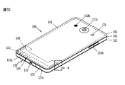
図1B及び図1Cを参照すると、移動端末機100は、ストレート型の端末機本体を備えている。ただし、本発明は、これに限定されるものではなく、ウォッチ型、クリップ型、グラス型、2つ以上の本体が相対移動可能に結合される折り畳み型、フリップ型、スライド型、スイング型、2軸回転型などの様々な構造に適用可能である。すなわち、ストレート型の移動端末機を一例として説明するが、当該説明は他のタイプの移動端末機にも一般的に適用可能である。
Referring to FIGS. 1B and 1C, the
ここで、端末機本体とは、移動端末機100を少なくとも1つの集合体とみなしてそれを示す概念である。
Here, the terminal body is a concept that regards the
移動端末機100は、外観を形成するケース(例えば、フレーム、ハウジング、カバーなど)を含む。同図に示すように、移動端末機100は、フロントケース101とリアケース102とを含んでもよい。フロントケース101とリアケース102との結合により形成される内部空間には、各種電子部品が配置される。フロントケース101とリアケース102との間には、1つ又は複数のミドルケースがさらに配置されてもよい。
The
端末機本体の前面には、情報を出力できるようにディスプレイ部151が配置されてもよい。同図に示すように、ディスプレイ部151のウィンドウ151aは、フロントケース101に装着されてフロントケース101と共に端末機本体の前面を形成するようにしてもよい。
A
場合によっては、リアケース102にも電子部品が装着される。リアケース102に装着可能な電子部品としては、着脱可能なバッテリ、識別モジュール、メモリカードなどがある。この場合、リアケース102には、装着された電子部品を覆うための背面カバー103が着脱可能に結合される。つまり、背面カバー103がリアケース102から分離した場合、リアケース102に装着された電子部品が外部に露出する。
In some cases, electronic components are also attached to the
同図に示すように、背面カバー103がリアケース102に結合された場合、リアケース102の側面の一部が露出する。場合によっては、結合時、リアケース102が背面カバー103により完全に遮蔽される。また、背面カバー103には、カメラ121bや音響出力部152bを外部に露出させるための開口部が備えられてもよい。
As shown in the figure, when the
これらのケース101、102、103は、合成樹脂を射出して形成してもよく、金属、例えばステンレススチール、アルミニウム(Al)、チタン(Ti)などで形成してもよい。
These
移動端末機100は、複数のケースが各種電子部品を収容する内部空間を形成する前記例とは異なり、1つのケースが内部空間を形成するように構成されてもよい。この場合、合成樹脂又は金属が側面から背面につながるユニボディの移動端末機100が実現される。
The
さらに、移動端末機100は、端末機本体の内部に水が入り込まないようにする防水部(図示せず)を含んでもよい。例えば、防水部は、ウィンドウ151aとフロントケース101との間、フロントケース101とリアケース102との間、又はリアケース102と背面カバー103との間に備えられ、これらの結合時に内部空間を密閉する防水部材を含んでもよい。
Furthermore, the
さらに、移動端末機100は、ディスプレイ部151、第1音響出力部152a及び第2音響出力部152b、近接センサ141、照度センサ142、光出力部154、第1カメラ121a及び第2カメラ121b、第1操作ユニット123a及び第2操作ユニット123b、マイク122、インタフェース部160などを含んでもよい。
The
以下、図1B及び図1Cに示すように、端末機本体の前面にディスプレイ部151、第1音響出力部152a、近接センサ141、照度センサ142、光出力部154、第1カメラ121a及び第1操作ユニット123aが配置され、端末機本体の側面に第2操作ユニット123b、マイク122及びインタフェース部160が配置され、端末機本体の背面に第2音響出力部152b及び第2カメラ121bが配置された移動端末機100を一例として説明する。
Hereinafter, as shown in FIGS. 1B and 1C, the
ただし、移動端末機100のこれらの構成要素は、前記配置に限定されるものではなく、必要に応じて除外又は代替されたり、他の面に配置されてもよい。例えば、第1操作ユニット123aが端末機本体の前面に備えられず、第2音響出力部152bが端末機本体の背面ではなく端末機本体の側面に備えられるようにしてもよい。
However, these components of the
ディスプレイ部151は、移動端末機100で処理される情報を表示(出力)する。例えば、ディスプレイ部151は、移動端末機100で起動されるアプリケーションプログラムの実行画面情報、又は当該実行画面情報に応じたUI(User Interface)、GUI(Graphic User Interface)情報を表示する。
The
ディスプレイ部151は、液晶ディスプレイ(Liquid Crystal Display; LCD)、薄膜トランジスタ液晶ディスプレイ(Thin Film Transistor-Liquid Crystal Display; TFT-LCD)、有機発光ダイオード(Organic Light-Emitting Diode; OLED)、フレキシブルディスプレイ、3次元ディスプレイ、電子インクディスプレイの少なくとも1つを含む。
The
ディスプレイ部151は、移動端末機100の実現形態に応じて2つ以上備えられてもよい。この場合、移動端末機100には、複数のディスプレイ部を1つの面に離隔して又は一体に配置してもよく、異なる面にそれぞれ配置してもよい。
Two or
ディスプレイ部151は、タッチ方式で制御命令の入力を受けることができるように、ディスプレイ部151へのタッチを感知するタッチセンサを含んでもよい。よって、ディスプレイ部151へのタッチが行われると、タッチセンサは、タッチを感知し、制御部180は、それに基づいてタッチに対応する制御命令を発生するようにすることができる。タッチ方式で入力される内容は、文字、数字、各種モードの指示、又は指定可能なメニュー項目などである。
The
タッチセンサは、タッチパターンを備えるフィルム状に構成されてウィンドウ151aとウィンドウ151aの背面上のディスプレイ151との間に配置されてもよく、ウィンドウ151aの背面に直接パターニングされるメタルワイヤで構成されてもよい。また、タッチセンサは、ディスプレイ151と一体に形成されてもよい。例えば、タッチセンサは、ディスプレイ151の基板上に配置されてもよく、ディスプレイ151の内部に備えられてもよい。
The touch sensor may be configured in a film shape with a touch pattern and may be disposed between the
このように、ディスプレイ部151は、タッチセンサと共にタッチスクリーンを実現することができる。この場合、タッチスクリーンは、ユーザ入力部123(図1A参照)として機能することができる。場合によっては、タッチスクリーンは、第1操作ユニット123aの少なくとも一部の機能を代替することができる。
Thus, the
第1音響出力部152aは、通話音をユーザの耳に伝えるレシーバで実現し、第2音響出力部152bは、各種アラーム音やマルチメディアの再生音を出力するラウドスピーカの形態で実現してもよい。
The first
ディスプレイ部151のウィンドウ151aには、第1音響出力部152aから発生する音響の放出のための音響ホールが形成されてもよい。しかし、本発明は、これに限定されるものではなく、第1音響出力部152aから発生する音響が構造物間の組立隙間(例えば、ウィンドウ151aとフロントケース101間の隙間)から放出されるようにしてもよい。この場合、音響の放出のために独立して形成されるホールが見えなくなるか又は隠れるので、移動端末機100の外観がよりシンプルになる。
In the
光出力部154は、イベントの発生時にそれを通知するための光を出力するように構成される。イベントの例としては、呼信号受信、メッセージ受信、不在着信、アラーム、スケジュール通知、電子メール受信、アプリケーションによる情報受信などが挙げられる。制御部180は、ユーザのイベント確認が感知されると光の出力が終了するように、光出力部154を制御することができる。
The
第1カメラ121aは、撮影モード又はテレビ電話モードでイメージセンサにより得られる静止画像又は動画像の画像フレームを処理する。第1カメラ121aで処理された画像フレームは、ディスプレイ部151に表示することができ、メモリ170に保存することもできる。
The
第1操作ユニット123a及び第2操作ユニット123bは、移動端末機100の動作を制御するための命令を入力するために操作するユーザ入力部123の一例であり、操作部ともいわれる。第1操作ユニット123a及び第2操作ユニット123bは、タッチ、プッシュ、スクロールなど、触知式(tactile manner)であればいかなるタッチ方式も採用可能である。また、第1操作ユニット123a及び第2操作ユニット123bは、近接タッチ(proximity touch)、ホバリングタッチなど、非触知式のタッチ方式も採用可能である。
The
同図においては、第1操作ユニット123aがタッチキーで構成された場合を例示しているが、本発明は、これに限定されるものではない。例えば、第1操作ユニット123aは、プッシュキー(メカニカルキー)で構成されてもよく、タッチキーとプッシュキーの組み合わせで構成されてもよい。
In the figure, although the case where the
第1操作ユニット123a及び第2操作ユニット123bにより入力される内容は多様に設定することができる。例えば、第1操作ユニット123aには、メニュー、ホームキー、キャンセル、検索などの命令が入力され、第2操作ユニット123bには、第1音響出力部152a又は第2音響出力部152bから出力される音響のボリューム調整、ディスプレイ部151のタッチ認識モードへの移行などの命令が入力される。
The contents input by the
また、端末機本体の背面には、ユーザ入力部123の他の例として、背面入力部(図示せず)が備えられてもよい。背面入力部は、移動端末機100の動作を制御するための命令を入力するために操作するものであり、背面入力部により入力される内容は多様に設定することができる。例えば、電源のオン/オフ、開始、終了、スクロールなどの命令、第1音響出力部152a又は第2音響出力部152bから出力される音響のボリューム調整、ディスプレイ部151のタッチ認識モードへの移行などの命令が入力される。背面入力部は、タッチ入力、プッシュ入力、又はそれらの組み合わせによる入力が可能な形態で実現することができる。
In addition, a rear surface input unit (not shown) may be provided on the rear surface of the terminal body as another example of the
背面入力部は、端末機本体の厚さ方向に前面のディスプレイ部151と重なるように配置されてもよい。例えば、ユーザが端末機本体を片手で握った場合に人差し指を用いて容易に操作できるように、背面入力部は、端末機本体の背面の上端部に配置されてもよい。ただし、本発明は、これに限定されるものではなく、背面入力部の位置は変更可能である。
The rear side input unit may be disposed to overlap the
このように端末機本体の背面に背面入力部が備えられた場合、それを用いた新しい形態のユーザインタフェースを実現することができる。また、タッチスクリーン又は背面入力部が端末機本体の前面に備えられた第1操作ユニット123aの少なくとも一部の機能を代替して、端末機本体の前面に第1操作ユニット123aが配置されない場合、ディスプレイ部151をより大画面に構成することができる。
As described above, when the rear side input unit is provided on the rear side of the terminal body, a new form of user interface using the same can be realized. Also, if the touch screen or the rear surface input unit substitutes at least a part of the function of the
さらに、移動端末機100は、ユーザの指紋を認識する指紋センサを含んでもよい。この場合、制御部180は、指紋センサにより感知される指紋情報を認証手段として用いることができる。指紋センサは、ディスプレイ部151又はユーザ入力部123に内蔵されてもよい。
Furthermore, the
マイク122は、ユーザの音声、その他の音などを入力できるように構成される。マイク122は、複数箇所に備えられてステレオ音響を入力できるように構成されてもよい。
The
インタフェース部160は、移動端末機100を外部機器に接続するための通路となる。例えば、インタフェース部160は、他の装置(例えば、イヤホン、外部スピーカなど)との接続のための接続端子、近距離通信のためのポート(例えば、赤外線ポート、ブルートゥースポート、無線LANポートなど)、又は移動端末機100への電源供給のための電源供給端子の少なくとも1つである。インタフェース部160は、SIM(Subscriber Identity Module)、UIM(User Identity Module)、情報保存のためのメモリカードなどの外部カードを収容するソケットの形態で実現してもよい。
The
端末機本体の背面には、第2カメラ121bが配置されてもよい。この場合、第2カメラ121bは、第1カメラ121aとは撮影方向が実質的に反対である。
The
第2カメラ121bは、少なくとも1つのラインに沿って配列される複数のレンズを含んでもよい。複数のレンズは、マトリクス状に配列されてもよい。このようなカメラを「アレイカメラ」ともいう。第2カメラ121bがアレイカメラで構成された場合、複数のレンズを用いて様々な方式で画像を撮影することができ、よりよい品質の画像を取得することができる。
The
フラッシュ124は、第2カメラ121bに隣接して配置されてもよい。フラッシュ124は、第2カメラ121bで被写体を撮影する場合に被写体に向けて光を照射する。
The
端末機本体には、第2音響出力部152bがさらに配置されてもよい。第2音響出力部152bは、第1音響出力部152aと共にステレオ機能を実現することができ、通話時にはスピーカフォンモードの実現のために用いることができる。
A second
端末機本体には、無線通信のための少なくとも1つのアンテナが備えられてもよい。アンテナは、端末機本体に内蔵されてもよく、ケースに形成されてもよい。例えば、放送受信モジュール111の一部を構成するアンテナは、端末機本体から引き出し可能に構成されてもよい。また、アンテナは、フィルム状に形成されて背面カバー103の内面に取り付けられてもよく、導電性材質を含むケースがアンテナとして機能するように構成されてもよい。
The terminal body may be equipped with at least one antenna for wireless communication. The antenna may be built in the terminal body or may be formed in a case. For example, the antenna which constitutes a part of the
端末機本体には、移動端末機100に電源を供給するための電源供給部190が備えられてもよい。電源供給部190は、端末機本体に内蔵されてもよく、端末機本体の外部に着脱可能に構成されるバッテリ191を含んでもよい。
The terminal body may include a
バッテリ191は、インタフェース部160に接続される電源ケーブルを介して電源が供給されるように構成されてもよい。また、バッテリ191は、無線充電機器により無線充電可能に構成されてもよい。無線充電は、電磁誘導方式又は磁界共振方式(電磁界共鳴方式)で実現することができる。
The
同図においては、背面カバー103がバッテリ191を覆うようにリアケース102に結合されてバッテリ191の離脱を制限し、バッテリ191を外部の衝撃と異物から保護するように構成された場合を例示している。バッテリ191が端末機本体に着脱可能に構成された場合、背面カバー103がリアケース102に着脱可能に結合されるようにしてもよい。
In the figure, the
さらに、移動端末機100は、外観を保護したり、移動端末機100の機能を補助又は拡張するためのアクセサリーを含んでもよい。アクセサリーの一例としては、移動端末機100の少なくとも一面を覆蓋又は収容するカバー又はパウチが挙げられる。カバー又はパウチは、ディスプレイ部151と連動して移動端末機100の機能を拡張するように構成されてもよい。アクセサリーの他の例としては、タッチスクリーンへのタッチ入力を補助又は拡張するためのタッチペンが挙げられる。
Furthermore, the
以下、このように構成された移動端末機で実現できる制御方法に関する実施形態について添付図面を参照して説明する。本発明の思想及び必須の特徴を逸脱しない範囲で本発明の他の特定の形態への具体化が可能であることは、当業者にとって自明である。 Hereinafter, an embodiment of a control method that can be realized by the mobile terminal configured as described above will be described with reference to the attached drawings. It will be apparent to those skilled in the art that the present invention can be embodied in other specific forms without departing from the spirit and essential characteristics of the present invention.
まず、本発明の第1実施形態について説明する。 First, a first embodiment of the present invention will be described.
図2A〜図2Dは本発明の第1実施形態による移動端末機の分解斜視図である。 2A to 2D are exploded perspective views of a mobile terminal according to a first embodiment of the present invention.
同図を参照すると、移動端末機100は、ディスプレイ部151を構成するウィンドウ151a及びディスプレイモジュール151bを含む。ウィンドウ151aはフロントケース101の一面に結合されてもよい。
Referring to the figure, the
フロントケース101とリアケース102との間には、電気素子を支持するためのフレーム185が配置される。フレーム185は、移動端末機100の内部支持構造であり、一例として、ディスプレイモジュール151b、カメラモジュール121b、アンテナモジュール130、バッテリ191及びプリント基板181の少なくとも1つを支持できるように形成される。
A
フレーム185は、その一部が移動端末機100の外部に露出するようにしてもよい。なお、フレーム185は、スライド型の移動端末機に適用した場合、本体部とディスプレイ部とを連結するスライドモジュールの一部を構成するようにしてもよい。
The
図2A〜図2Dには、リアケース102とプリント基板181との間にフレーム185が配置され、プリント基板181の一面にディスプレイモジュール151bが結合された場合を例示している。リアケース102にはバッテリ191を覆うように背面カバー103が結合される。ここで、フレーム185は、移動端末機100の剛性を向上させるための部品である。
FIGS. 2A to 2D illustrate the case where the
ウィンドウ151aはフロントケース101の一面に結合される。ウィンドウ151aにはタッチセンサ(図示せず)が取り付けられてもよい。タッチセンサは、タッチ入力を感知するように構成され、光透過性に形成される。タッチセンサは、ウィンドウ151aの前面に取り付けられ、ウィンドウ151aの特定部位に発生する電圧などの変化を電気的な入力信号に変換するように構成されてもよい。
The
ディスプレイモジュール151bはウィンドウ151aの背面に取り付けられる。本実施形態においては、ディスプレイモジュール151bの例として薄膜トランジスタ液晶ディスプレイ(TFT−LCD)を挙げるが、本発明は必ずしもこれに限定されるものではない。
The
例えば、ディスプレイモジュール151bは、液晶ディスプレイ(LCD)、有機発光ダイオード(OLED)、フレキシブルディスプレイ、3次元ディスプレイなどであってもよい。
For example, the
プリント基板181は、ディスプレイモジュール151bの下部に取り付けられてもよい。また、プリント基板181の背面上には少なくとも1つの電子素子が装着される。
The printed
フレーム185には、バッテリ191を収容できるように凹んだ収容部が形成されてもよい。リアケース102又はフレーム185の一側面には、バッテリ191が端末機本体に電源を供給するようにプリント基板181に接続される接触端子が形成されてもよい。
The
移動端末機100の上端又は下端にはアンテナモジュール130が配置されてもよい。
An
一般的に、移動端末機100の上端にはLTE/WCDMA Rx Onlyアンテナ、GPSアンテナ、BT/WiFiアンテナなどが配置され、移動端末機100の下端にはメインアンテナが配置される。
Generally, an LTE / WCDMA Rx Only antenna, a GPS antenna, a BT / WiFi antenna, etc. are disposed at the upper end of the
本発明の実施形態は、主にメインアンテナに関するものであるが、必ずしもこれに限定されるものではなく、周波数帯域によってLTE/WCDMA Rx Onlyアンテナ、GPSアンテナ、BT/WiFiアンテナの少なくとも1つの周波数帯域を送受信することもできる。 Embodiments of the present invention mainly relate to the main antenna, but are not necessarily limited thereto, and at least one frequency band of the LTE / WCDMA Rx Only antenna, the GPS antenna, and the BT / WiFi antenna depending on the frequency band. Can also be sent and received.
また、アンテナモジュール130は、複数備えられて移動端末機100の各端部に配置され、各アンテナモジュール130が異なる周波数帯域の無線信号を送受信するようにしてもよい。
Also, a plurality of
フレーム185は、薄く形成されても十分な剛性を維持できるように、金属で形成されてもよい。金属製のフレーム185は、グランドとして動作することができる。すなわち、プリント基板181又はアンテナモジュール130がフレーム185に接地接続され、フレーム185がプリント基板181又はアンテナモジュール130のグランドとして動作するようにすることができる。この場合、フレーム185は、移動端末機100のグランドを拡張する。
The
なお、フレーム185を備えるのではなく、プリント基板181が端末機本体のほとんどの面積を占めるように構成された場合は、プリント基板181自体でグランドを拡張することができる。
When the printed
プリント基板181は、アンテナモジュール130に電気的に接続され、アンテナモジュール130により送受信される無線信号(又は無線電磁波)を処理する。無線信号の処理のために、プリント基板181には複数の送受信回路182が形成又は装着されてもよい。
The printed
送受信回路182は、少なくとも1つの集積回路及び関連電気素子を含んでもよい。例えば、送受信回路182は、送信集積回路、受信集積回路、スイッチング回路、増幅器などを含んでもよい。
The transmit and receive
複数の送受信回路182は、放射体である導電部材に同時に給電することにより、複数のアンテナモジュール130が同時に作動するようにしてもよい。例えば、複数の送受信回路182は、いずれか一方が送信する間、他方は受信するようにしたり、両方とも送信するようにしたり、両方とも受信するようにすることができる。
The plurality of transmitting and receiving
各送受信回路182は、CP(Call Processor)、モデムチップ、RFトランシーバチップ及びRFレシーバチップの少なくとも1つを含む通信チップの形態で実現してもよい。よって、各通信チップは、給電部とマッチングモジュール(可変スイッチを含む)を介して導電部材に給電することにより無線信号を送信したり、導電部材により受信された無線信号をマッチングモジュール(可変スイッチを含む)と給電部を介して受けて周波数変換処理や復調処理などの所定の受信処理を行うことができる。
Each transmission /
同軸ケーブル183、184は、プリント基板181と各アンテナモジュール130とを接続する。例えば、同軸ケーブル183、184は、アンテナモジュール130に給電する給電装置に接続されてもよい。給電装置は、第1操作ユニット123aから入力される信号を処理するように構成されるフレキシブルプリント基板186の一面に備えられてもよい。フレキシブルプリント基板186の他面は、第1操作ユニット123aの信号を伝達するように構成される信号伝達ユニット123cに結合されてもよい。この場合、フレキシブルプリント基板186の他面にドームが形成され、信号伝達ユニット123cにアクチュエータが備えられるようにしてもよい。
The
本発明の実施形態においては、移動端末機100の外観を形成する金属枠を活用するアンテナモジュール130を提供する。例えば、移動端末機100の外観を形成する側面の一部又は全部をアンテナとして活用することができる。
In an embodiment of the present invention, an
以下、図2A〜図2D及び図3を参照して本発明の第1実施形態について説明する。図3は本発明の第1実施形態によるアンテナモジュールの平面図である。図3は図2Aのアンテナモジュール130を示す図であるが、図2B〜図2Dの移動端末機100のアンテナモジュール130も図2Aの移動端末機100と部分的に異なるにすぎないので、以下では図3を図2A〜図2Dのアンテナモジュール130の平面図とみなして説明する。
Hereinafter, a first embodiment of the present invention will be described with reference to FIGS. 2A to 2D and FIG. FIG. 3 is a plan view of the antenna module according to the first embodiment of the present invention. FIG. 3 is a view showing the
本発明の第1実施形態によるアンテナモジュール130は、給電部137及び接地部138に接続される第1導電部材131と、第1導電部材131から離隔して配置される第2導電部材132と、給電部137に近い位置で第1導電部材131と第2導電部材132とを接続する第1接続部材133と、接地部138に近い位置で第1導電部材131と第2導電部材132とを接続する第2接続部材134とを含む。ここで、給電部137と接地部138とは、第1導電部材131及び第2導電部材132の形成方向に所定間隔離隔している。
The
第1導電部材131及び第2導電部材132は、アンテナモジュール130の放射体として動作するようにしてもよい。一例として、第1導電部材131及び第2導電部材132は、折り返しダイポールアンテナ(folded dipole antenna)の放射体として動作するようにしてもよい。また、第1導電部材131及び第2導電部材132は、金属パターンからなるようにしてもよく、一例としてマイクロストリップであってもよい。
The first
折り返しダイポールアンテナは、入力抵抗の大きさが一般的な半波長ダイポールアンテナの約4倍であるので、放射電力及び放射抵抗も半波長ダイポールアンテナより大きい。よって、特性インピーダンスの高い給電線との整合が容易になるので、広帯域特性を実現することができる。 Since the size of the input resistance of the folded dipole antenna is about four times that of a general half-wave dipole antenna, the radiation power and the radiation resistance are also larger than the half-wave dipole antenna. Therefore, since matching with a feed line having a high characteristic impedance is facilitated, a wide band characteristic can be realized.
さらに、第1導電部材131及び第2導電部材132は、プリント基板181に隣接して配置される。ここで、第2導電部材132は、少なくとも一部がプリント基板181と重なるように配置されてもよい。
Furthermore, the first
給電部137は、放射体として動作する各部材に電流を供給する部分であり、バルーン、移相器、分配器、減衰器、増幅器などを組み合わせて構成してもよい。これは、後述する給電部237a、237bについても同様である。
The feeding
第1導電部材131及び第2導電部材132への給電方式は特に限定されない。例えば、第1導電部材131又は第2導電部材132に給電部137を電気的に接続して給電する方式や、EM(Electro-Magnetic)給電方式を用いることができる。ただし、本発明の第1及び第2実施形態においては、空間が狭いことから第1導電部材131、231と第2導電部材132、232との間に干渉が生じることがあるので、第1導電部材131、231及び第2導電部材132、232への給電としては、給電ラインによる直接給電(direct feeding)が好ましい。
The power feeding method to the first
よって、以下では直接給電方式の給電を中心に説明する。直接給電方式の給電のために、給電ライン137aは、給電板、給電用クリップ又は給電線の少なくとも1つを含む。ここで、給電ライン137aが給電板、給電用クリップ又は給電線の2つ以上を含む場合は、これらが互いに電気的に接続され、給電装置から給電される電流(又は電圧)を無線信号の送受信を行う導電部材に送る。ここで、給電線は、基板に印刷されるマイクロストリップを含んでもよい。
Therefore, in the following, the description will focus on the direct feeding method. The
ここで、第1導電部材131は第1部分131aと第2部分131bとに分けられるが、第1部分131aと第2部分131bとは所定間隔(D)離隔してスリット105を形成し、スリット105は給電部137と接地部138との間に形成される。このように、本発明の第1実施形態においては、第1導電部材131にスリット105が形成されるが、これは、第1導電部材131の長さをより短くして高周波帯域の周波数をより容易に実現できるようにするためである。ここで、スリット105は、十分な長さを有し、第1部分131aと第2部分131bとの間で電気的結合が生じないようにすることが好ましい。もし、第1部分131aと第2部分131bとの間で電気的結合が生じると、低周波又は高周波帯域の共振周波数の実現が困難になるので、第1部分131aと第2部分131bとは電気的結合が生じない程度に離隔しなければならない。
Here, although the first
図2Aは本発明の第1実施形態に関するものであり、第1導電部材131が端末機本体の側面外観を形成し、第2導電部材132がリアケース102に形成された場合を例示している。ここで、第1導電部材131が端末機本体の側面外観の一部又は全部を形成するが、端末機本体の側面外観の全部を形成した場合は外観上の一体性を持たせることができる。ただし、この場合、アンテナモジュール130においては、第1接続部材133及び第2接続部材134が第1導電部材131と第2導電部材132とを接続することにより、第1導電部材131が電気的に分離されるようにする。
FIG. 2A relates to the first embodiment of the present invention, and illustrates the case where the first
図2Bは本発明の第1実施形態に関するものであり、第1導電部材131が端末機本体の側面外観の一部を形成し、残部102bとは絶縁材102aにより分離されるようにした場合を例示している。残部102bの一地点はプリント基板181に接地されている。ここで、残部102bはメタルデコ(metal deco)であってもよい。残部102bは、第1導電部材131又は第2導電部材132と共にリアケース102を形成する。すなわち、残部102bは、第1導電部材131(図2Cのように、第2導電部材132が端末機本体の側面外観を形成し、第1導電部材131がリアケース102に形成された場合は、第2導電部材132)に連結されて端末機本体の側面外観を形成する。
FIG. 2B relates to the first embodiment of the present invention, in which the first
ここで、残部102bは、第1導電部材131を連結するループ状に形成されてもよく、インサート射出により一体に形成されたリアケース102として形成されてもよい。これは、特に断らない限り他の実施形態においても同様である。
Here, the remaining portion 102b may be formed in a loop shape connecting the first
図2Cは本発明の第1実施形態に関するものであり、第1導電部材131及び第2導電部材132が図2A及び図2Bとは逆の位置に形成された場合を例示している。なお、第1導電部材131及び第2導電部材132の位置を除いては、図2A及び図2Bと同様である。つまり、本発明の第1実施形態において、第1導電部材131及び第2導電部材132は、いずれか一方を端末機本体の側面外観に形成し、他方を端末機本体の内部に形成すればよく、第1導電部材131又は第2導電部材132にスリット105が形成されて所定間隔離隔していればよい。
FIG. 2C relates to the first embodiment of the present invention, and illustrates the case where the first
図2Dは本発明の第1実施形態に関するものであり、第2導電部材132、第3接続部材135及びサブアーム136が背面カバー103に形成された場合を例示している。すなわち、第1導電部材131は端末機本体の側面外観の一部又は全部を形成し、第2導電部材132は背面カバー103の内側に取り付けられている。ここで、サブアーム136は寄生共振のためのブランチ機能を有する。
FIG. 2D relates to the first embodiment of the present invention, and illustrates the case where the second
以上のように、第1導電部材131及び第2導電部材132は、いずれかが端末機本体の側面外観の一部又は全部を形成し、第1導電部材131もしくは第2導電部材132、第3接続部材135及びサブアーム136が背面カバー103又はリアケース102に形成されるようにしてもよい。さらに、第1導電部材131又は第2導電部材132は、リアケース102の内面又は外面に形成されてもよく、端末機本体の側面を形成する場合も必ずしも最外郭に形成される必要はない。例えば、第1導電部材131が端末機本体の側面を形成する場合、側面の最外郭には射出物が形成され、射出物の内部に第1導電部材131が形成されてもよい。
As described above, either of the first
つまり、本発明の第1実施形態においては、第1導電部材131と第2導電部材132とが所定間隔離隔していればよく、必ずしも端末機本体の外観を形成する必要はない。
That is, in the first embodiment of the present invention, the first
給電部137は、第1導電部材131に給電して様々な長さのアンテナループを形成させる。このような構成により、低周波及び高周波帯域の周波数を実現することができる。
The
図2A〜図2Dに示すものは例示にすぎず、特に断らない限り異なる実施形態に重複して適用することができる。これは、第2実施形態においても同様である。例えば、第2実施形態において、第1導電部材231が端末機本体の側面外観の一部又は全部を形成し、第2導電部材232が端末機本体の内部に配置されるようにしてもよい。
What is shown in FIGS. 2A to 2D is merely an example, and can be applied to different embodiments in duplicate unless otherwise specified. The same applies to the second embodiment. For example, in the second embodiment, the first
プリント基板181は、フレキシブルプリント基板であってもよい。基板は、誘電体基板又は半導体基板であってもよく、基板のいずれか一面にグランドが形成されてもよく、多層基板の場合、基板のいずれかの層がグランドとなってもよい。また、本発明の第1実施形態において、第1導電部材131及び第2導電部材132は、プリント基板181に沿って折り曲げられるが、これは端末機本体の構造に対応させるためのものである。
The printed
図4A〜図4Fは本発明の第1実施形態における共振周波数の共振経路を示す図である。 4A to 4F are diagrams showing resonance paths of resonance frequencies in the first embodiment of the present invention.
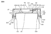
図4Aは最も低い周波数である第1共振周波数F11を実現できる第1共振経路L11を示すものである。第1共振経路L11は、第1導電部材131、第2導電部材132、第1接続部材133及び第2接続部材134を通る電流により形成される。ここで、第1部分131aと第2部分131bとが離隔形成されることにより、第1共振経路L11は、給電部137と接地部138につながる経路を含む。これは、後述する第1実施形態における全ての共振経路において同様である。
FIG. 4A shows a first resonance path L11 which can realize the first resonance frequency F11 which is the lowest frequency. The first resonance path L11 is formed by the current passing through the first
本発明の第1実施形態においては、第1導電部材131のうち第1接続部材133が接続される部分1318の位置は、第1導電部材131のうち給電部137が接続される部分1315と第1導電部材131の端部との間で可変である。第2導電部材132のうち第1接続部材133が接続される部分の位置は、特に限定されないが、第1導電部材131に最も近い部分1323に接続されることが好ましい。これは、後述するように、第1接続部材133がネジ、Cクリップ、ポゴピン、EMIシートなどであり得るからである。ただし、第1接続部材133がネジ、Cクリップ、ポゴピン又はEMIシートに限定されるものではない。また、第1導電部材131と第2導電部材132とは導電パターンにより接続されてもよいが、この場合は、第1接続部材133が第1導電部材131と第2導電部材132との最近接点に形成されなくてもよい。
In the first embodiment of the present invention, the position of the
これは、後述する第2接続部材134及び第3接続部材135も同様である。図2A〜図2Dは第3接続部材135が導電パターンである場合を例示する。
The same applies to the
また、第1導電部材131のうち第2接続部材134が接続される部分1319の位置は、第1導電部材131のうち接地部138が接地ライン138aを介して接続される部分1316と第1導電部材131の端部との間で可変である。
Further, the position of the
さらに、第1接続部材133及び第2接続部材134の形成位置を変化させることにより、周波数帯域を変化させることができる。すなわち、図4Aに示すように、第1接続部材133は、第1導電部材131及び/又は第2導電部材132の端部に形成されてもよく、第1導電部材131及び/又は第2導電部材132の中間のいずれか一地点に形成されてもよい。第1接続部材133が第1導電部材131及び/又は第2導電部材132の中間のいずれか一地点に形成された場合は、第1〜第4寄生アーム(parasitic arm)1313、1314、1321、1322が形成されてもよい。このように、第1接続部材133及び第2接続部材134を微細に移動させることにより、周波数をチューニングすることができる。さらに、第1〜第4寄生アーム1313、1314、1321、1322により周波数帯域の効率及びインピーダンス特性を決定付けることもできる。ここで、第1〜第4寄生アーム1313、1314、1321、1322は、第1接続部材133及び第2接続部材134を越えた部分を意味する。
Furthermore, by changing the formation positions of the
図4Bは第2共振周波数F12を実現できる第2共振経路L12を示すものである。第2共振周波数F12は第1共振周波数F11より高い周波数である。第2共振周波数F12は、第1導電部材131、第2導電部材132、第1接続部材133及び第3接続部材135により形成される。
FIG. 4B shows a second resonance path L12 that can realize the second resonance frequency F12. The second resonant frequency F12 is a frequency higher than the first resonant frequency F11. The second resonance frequency F12 is formed by the first
一般的に、より高い共振周波数を実現するためにはより短い共振経路が必要である。本発明の第1実施形態においては、第3接続部材135を形成することにより、第2共振経路L12を実現する。
Generally, shorter resonant paths are needed to achieve higher resonant frequencies. In the first embodiment of the present invention, by forming the
すなわち、本発明の第1実施形態によるアンテナモジュール130は、一端部が第1導電部材131に接続され、他端部が第2導電部材132に接続される第3接続部材135をさらに含んでもよい。ここで、第1導電部材131のうち第3接続部材135が接続される部分1317の位置は、第1導電部材131のうち接地部138が接地ライン138aを介して接続される部分1316と第2接続部材134が接続される部分1319との間で可変であり、第2導電部材132のうち第3接続部材135が接続される部分1325の位置は、第2導電部材132のうち第1接続部材133が接続される部分1323と第2接続部材134が接続される部分1324との間で可変である。ただし、第2導電部材132のうち第3接続部材135が接続される部分1325の位置は、第2接続部材134が接続される部分1324に近いことが好ましい。もし、第2導電部材132のうち第3接続部材135が接続される部分1325の位置が第2導電部材132のうち第1接続部材133が接続される部分1323に近い場合は、共振長さが変化して共振周波数が変化するからである。ただし、所望の共振周波数を得るために多少の位置変更は可能である。
That is, the
第2共振経路L12は、第1共振経路L11と同様に、第1導電部材131に形成されたスリット105の影響を受けて給電部137と接地部138間を流れる経路を含む。
Similar to the first resonance path L11, the second resonance path L12 includes a path that flows between the feeding
一方、本発明の第1実施形態によるアンテナモジュール130は、折り返しダイポールアンテナの一種であるので、第1導電部材131及び第2導電部材132は、第1周波数及び第2周波数で共振するように所定の長さに形成されるが、共振のためのアンテナ長は第1周波数及び第2周波数に対応するλ/2程度となるようにする。ただし、後述するようにモノポールアンテナとして動作する場合は、アンテナ長がλ/4程度となるようにする。ここで、第1周波数は低周波数であり、第2周波数は第1周波数より高い高周波数であるが、第1周波数の周波数帯域は低周波数帯域である約700〜1200MHzであり、第2周波数の周波数帯域は高周波数帯域である約1710〜27000MHzである。なお、周波数帯域は、より細分して、約700〜1000MHzの低周波数帯域、約1700〜2200MHzの中周波数帯域、及び約2200〜2700MHzの高周波数帯域に分けることもできる。
Meanwhile, since the
さらに図4Aを参照して電流の流れを説明する。第1導電部材131に給電された電流は第1接続部材133を介して第2導電部材132に流れる。第2導電部材132に流れてきた電流は第2接続部材134を介して再び第1導電部材131に流れ、その後接地部138を介してプリント基板181のグランドに流れる。
The flow of current is further described with reference to FIG. 4A. The current supplied to the first
このような電流の流れに基づいてアンテナモジュール130を他の観点から見ると、第1導電部材131及び第2導電部材132に同一方向に電流が流れるといえる。すなわち、本発明の第1実施形態によるアンテナモジュール130は、半波長ダイポールアンテナを折り返した構造の折り返しダイポールアンテナとして機能することができるが、第1導電部材131と第2導電部材132とは電気的に対称であってもよい。これは、後述する第2実施形態においても同様である。
When the
このような折り返しダイポールアンテナにおいては、特定の共振周波数で第1導電部材131と第2導電部材132とが接続される部分1318には電流がほとんど流れない。すなわち、第1導電部材131に流れる電流と第2導電部材132に流れる電流とが逆方向であり、第1導電部材131と第2導電部材132とが接続される部分1318には電流がほとんど流れないヌルポイント(current null point)が発生する。この場合は、第1導電部材131にのみ共振経路が形成されるものと理解できる。すなわち、図4Cに示すように、第1導電部材131に第3共振経路L13が形成されるが、第1導電部材131のスリット105付近では給電部137と接地部138とを接続する経路として形成される。
In such a folded dipole antenna, almost no current flows in a
また、本発明の第1実施形態においては、第1導電部材131にスリット105が形成されているが、図4Dに示すように、給電部137と第1導電部材131とを接続する給電ライン137aとスリット105を形成する第2部分131bの開放端1311とにより第4共振経路L14が形成され、第4共振周波数F14が実現される。
Moreover, in the first embodiment of the present invention, the
さらに、図4Eに示すように、接地部138と第1導電部材131とを接続する接地ライン138aとスリット105を形成する第1部分131aの開放端1312とにより第5共振経路L15が形成され、第5共振周波数F15が実現される。本発明の第1実施形態における接地ライン138aは、接地部138と第1導電部材131とを接続する電気的通路であって、接地板、接地用クリップ又は接地線の少なくとも1つを含んでもよい。これは、本発明の第1及び第2実施形態における全ての接地部において同様である。
Furthermore, as shown in FIG. 4E, a fifth resonance path L15 is formed by the
それに加え、本発明の第1実施形態においては、より高い共振周波数を実現するために、第1導電部材131にサブアーム136を形成してもよい。すなわち、本発明の第1実施形態によるアンテナモジュール130は、一端部が第1導電部材131に接続され、他端部が開放されるサブアーム136をさらに含んでもよい。ここで、サブアーム136の一端部1320は、第1導電部材131のうち接地部138が接地ライン138aを介して接続される部分1316と第3接続部材135が接続される部分1317との間に形成される。サブアーム136により、図4Fに示すように、接地ライン138aから第1導電部材131を経てサブアーム136の開放端まで至る第6共振経路L16が形成され、第6共振周波数F16が実現される。
In addition, in the first embodiment of the present invention, the sub-arm 136 may be formed on the first
また、図11に示すサブアーム136’のように、一端部がプリント基板181に接地接続され、他端部が開放されるようにしてもよい。これについては後述する。
Further, as in the sub arm 136 'shown in FIG. 11, one end may be grounded to the printed
このように、本発明の第1実施形態においては、第1導電部材131にスリット105を形成することにより、低周波帯域だけでなく、高周波帯域の周波数の実現を容易にした。
As described above, in the first embodiment of the present invention, by forming the
ただし、サブアーム136の一端部1320の位置が前記に限定されるものではない。例えば、サブアーム136の一端部1320の位置は、第1導電部材131のうち第3接続部材135が接続される部分1317と第2接続部材134が接続される部分1319との間で可変であってもよい。ただし、サブアーム136の一端部1320の位置を変更すると、共振経路が変更され、共振周波数が変更される。
However, the position of the one
ここで、第4〜第6共振周波数F14、F15、F16は、端部が開放されているモノポールアンテナとして動作するので、アンテナ長は共振周波数に対応するλ/4程度である。 Here, since the fourth to sixth resonance frequencies F14, F15, and F16 operate as monopole antennas whose ends are open, the antenna length is about λ / 4 corresponding to the resonance frequency.
以下、前述した共振周波数をより広帯域化するためにチューニングする方法について説明する。 Hereinafter, a method of tuning to widen the resonance frequency described above will be described.
図10は本発明の第1実施形態によるアンテナモジュールの一部の概念図である。 FIG. 10 is a conceptual view of a part of the antenna module according to the first embodiment of the present invention.
図10を参照すると、第1導電部材131に給電するように給電部137に接続される給電ライン137aには、インピーダンスマッチングのための第1マッチングモジュール125aが配置され、第1マッチングモジュール125aには、第2部分131bに流れる電流を制御する第1可変スイッチ125bが直列又は並列に接続される。
Referring to FIG. 10, a
また、第1導電部材131を接地するように接地部138に接続される接地ライン138aには、インピーダンスマッチングのための第2マッチングモジュール126aが配置され、第2マッチングモジュール126aには、第1部分131aに流れる電流を制御する第2可変スイッチ126bが直列又は並列に接続される。さらに、サブアーム136には、サブアーム136に流れる電流を制御する第3可変スイッチ127が接続されてもよい。
In addition, a
具体的に示していないが、第3接続部材135に可変スイッチを接続してもよい。なお、第3接続部材135の形成位置を変更することにより所望の共振周波数を実現できるので、可変スイッチを接続しなくてもよい。
Although not specifically shown, a variable switch may be connected to the
第1マッチングモジュール125a及び第2マッチングモジュール126aは、インダクタ及びコンデンサを含む組み合わせからなり、直列素子や分路素子で構成されてもよい。直列素子で構成された場合は、インピーダンスの虚数部であるリアクタンス値が変更されることがある。例えば、インダクタはリアクタンスを上げ、コンデンサはリアクタンスを下げるので、特定の周波数帯域のインピーダンスが変更されることがある。これとは異なり、分路素子で構成された場合は、インピーダンスの実数部である抵抗値(レジスタンス値)が変更されることがある。例えば、インダクタは抵抗値を上げ、コンデンサは抵抗値を下げるので、特定の周波数帯域のインピーダンスが変更されることがある。
The
前述した第1実施形態は、第1導電部材131が端末機本体の側面を形成し、第2導電部材132が端末機本体の内部に配置された場合を例示するものである。図6は本発明の第1実施形態によるアンテナモジュールの一変形例の概念図であり、第1導電部材131及び第2導電部材132の位置が前述した場合と逆の場合、すなわち、第2導電部材132が端末機本体の側面を形成し、第1導電部材131が端末機本体の内部に配置された場合を例示する。
The first embodiment described above exemplifies the case where the first
第2導電部材132が端末機本体の側面外観を形成し、第1導電部材131が端末機本体の内部に配置された場合は、移動端末機の側面が滑らかな平面を形成するので外観が美麗である。これに関する移動端末機の分解斜視図は図2Cに示されている。この場合、スリット105は、第1部分131aと第2部分131bとの間で電気的結合が生じない程度の長さを有するようにしなければならない。
When the second
また、図2Aに示すように、第1導電部材131が端末機本体の側面外観を形成する場合は、スリット105の形成部分が問題となり得るが、スリット105の形成部分にはUSBポートなどのインタフェース部119を形成すればよいので、外観を大きく損なうことはない。すなわち、インタフェース部119の隣接部分は、第1部分131a及び第2部分131bとは分離しており、電流が流れない。
Also, as shown in FIG. 2A, when the first
しかし、図6及び図2Cに示すような場合は、スリット105が移動端末機100の内部に形成されており、外部に露出しない。
However, in the case shown in FIGS. 6 and 2C, the
図6には図4Aとの比較を容易にするために図4Aに示す部分のみを示し、図10及び図11に示す第1及び第2マッチングモジュール125a、126aと第1〜第3可変スイッチ125b、126b、127は示していないが、これらの構成の追加が特に限定されるものではない。すなわち、図6の変形例は、具体的に示していないが、図10及び図11に示す事項をそのまま適用可能である。例えば、図6の変形例においては、給電部137と第2部分131bとを接続する部分に第1マッチングモジュールを配置し、接地部138と第1部分131aとを接続する部分に第2マッチングモジュールを配置し、第1及び第2マッチングモジュールにそれぞれ第1及び第2可変スイッチを備えてもよい。さらに、図6の変形例においては、サブアーム136に第3可変スイッチを備えてもよい。
FIG. 6 shows only the portion shown in FIG. 4A to facilitate comparison with FIG. 4A, and the first and
図11は本発明の第1実施形態によるアンテナモジュールの他の変形例の概念図であり、サブアーム136’がグランドであるプリント基板181に接地接続され、サブアーム136’に可変スイッチ127’が接続された場合を例示する。このようにサブアーム136’と第2導電部材132とが近距離で離隔形成されることにより、電磁的結合(electromagnetic coupling)が生じて共振周波数帯域を追加することができる。電磁的結合がより生じやすくするために、サブアーム136’の少なくとも一部は第2導電部材132と平行に形成してもよい。
FIG. 11 is a conceptual diagram of another modification of the antenna module according to the first embodiment of the present invention, wherein the sub arm 136 'is grounded to the printed
図12は本発明の一実施形態による可変スイッチの種類を例示する図であり、インダクタ及び/又はコンデンサの様々な組み合わせの可変スイッチを例示する。例えば、図12の(a)に示すように、異なる大きさのインダクタを有するようにしてもよく、図12の(b)に示すように、インダクタ及びコンデンサを有するようにしてもよく、図12の(c)に示すように、1つのインダクタのみを有するようにしてもよい。また、図12の(d)に示すように、インダクタと可変コンデンサとを直列に接続してもよく、図12の(e)に示すように、可変コンデンサを有するようにしてもよく、図12の(f)に示すように、インダクタと可変コンデンサとを並列に接続してもよい。 FIG. 12 is a diagram illustrating the types of variable switches according to an embodiment of the present invention, illustrating variable switches of various combinations of inductors and / or capacitors. For example, as shown in FIG. 12A, inductors of different sizes may be provided, and as shown in FIG. 12B, an inductor and a capacitor may be provided. Only one inductor may be provided as shown in (c) of FIG. Further, as shown in (d) of FIG. 12, an inductor and a variable capacitor may be connected in series, and as shown in (e) of FIG. 12, a variable capacitor may be provided. As shown in (f), the inductor and the variable capacitor may be connected in parallel.
ただし、これらに限定されるものではなく、可変インダクタを用いてもよく、単極双投(Single Pole Double Throw; SPDT)スイッチや単極3投(Single Pole Triple Throw; SP3T)スイッチを用いてもよい。 However, the invention is not limited thereto, and a variable inductor may be used, and even if a single pole double throw (SPDT) switch or a single pole triple throw (SP3T) switch is used. Good.
このような可変スイッチは、本発明の属する技術の分野における通常の知識を有する者にとって自明なものであり、具体的な説明は省略する。 Such variable switches are obvious to those skilled in the art to which the present invention belongs, and a detailed description thereof will be omitted.
図5は本発明の第1実施形態によるアンテナモジュールの概念図及び部分拡大図であり、第1導電部材131が端末機本体の側面外観を形成し、第2導電部材132が端末機本体の内部に配置された場合を例示する。
FIG. 5 is a conceptual view and a partial enlarged view of an antenna module according to a first embodiment of the present invention, wherein the first
図7は本発明の第1実施形態によるアンテナモジュールにおける周波数と反射係数の関係を示すグラフであり、700MHz、800MHz、1200MHz付近でそれぞれ第1〜第3共振周波数F11、F12、F13で共振し、1900MHz、2200MHz、2700MHz付近でそれぞれ第4〜第6共振周波数F14、F15、F16で共振することが分かる。この結果は一実施形態にすぎず、本発明の権利範囲を解釈する上で共振周波数に限定されるものではない。 FIG. 7 is a graph showing the relationship between the frequency and the reflection coefficient in the antenna module according to the first embodiment of the present invention, which resonates at first to third resonance frequencies F11, F12 and F13 near 700 MHz, 800 MHz and 1200 MHz, It can be seen that resonance occurs at the fourth to sixth resonance frequencies F14, F15, and F16 near 1900 MHz, 2200 MHz, and 2700 MHz, respectively. This result is only an embodiment, and is not limited to the resonant frequency in interpreting the scope of the present invention.
一方、図8は図1CのA部の拡大図であり、図9Aは図8の第1導電部材を分離して示す概念図であり、図9B及び図9Cは図8の背面カバーを分離して示す概念図である。 8 is an enlarged view of a portion A of FIG. 1C, FIG. 9A is a conceptual view showing the first conductive member of FIG. 8 in isolation, and FIGS. 9B and 9C show the back cover of FIG. It is a conceptual diagram shown.
同図を参照すると、背面カバー103がリアケース102に結合されると、第1接続部材133により第1導電部材131と第2導電部材132とが電気的に接続される。以下に説明する構造は、第2接続部材134により第1導電部材131と第2導電部材132とが電気的に接続される構造にも同様に適用される。
Referring to the figure, when the
第1接続部材133は、背面カバー103及び第1導電部材131のいずれか一方に取り付けられ、他方との接触により第1導電部材131と第2導電部材132とを電気的に接続する。接触により第1導電部材131と第2導電部材132とが電気的に接続され、弾性変形により接触が堅固に維持される。本発明の実施形態においては、弾性変形のために、前述したように第1接続部材131及び第2接続部材134にCクリップ、ポゴピン又はEMIシートを用いてもよい。
The
第1接続部材133は、背面カバー103の内面に取り付けられてもよく、リアケース102に取り付けられてもよい。図8、図9A〜図9Cは第2接続部材134が背面カバー103に取り付けられ、第1接続部材133が第1導電部材131から突出するように第1導電部材131に取り付けられた場合を例示する。例えば、図9Aに示すように、第1接続部材133は、第1導電部材131に収容され、少なくとも一部133aが第1導電部材131から突出するように配置されてもよい。他の例として、第1接続部材133は、第1導電部材131の内面に結合され、少なくとも一部が第1導電部材131から突出するように配置されてもよく、第1導電部材131の上面を覆うように配置されてもよい。
The
また、第1接続部材133は、背面カバー103及び第1導電部材131のいずれかから突出し、他方に形成された凹部103aに挿入されてもよい。例えば、図9Bに示すように、背面カバー103の内面に第1接続部材133に対応する凹部103aが形成されてもよい。この場合、背面カバー103がリアケース102に結合されると、凹部103aに第1接続部材133が収容される。
In addition, the
さらに、第2導電部材132の一部が凹部103aから外部に露出するようにしてもよい。すなわち、第2導電部材132は、凹部103aの底部を形成するようにしてもよい。
Furthermore, a part of the second
一方、図9Cに示すように、第2導電部材132の一部が背面カバー103の端部をまたぐように形成されてもよい。この場合は、リアケース102に形成される第1接続部材133が外部に少しだけ露出していても第1接続部材133と第2導電部材132とを電気的に接続することができる。
On the other hand, as shown in FIG. 9C, a part of the second
つまり、本発明の実施形態においては、第1導電部材131と第2導電部材132との接続方式に特に制限はない。
That is, in the embodiment of the present invention, the connection method of the first
図8に示すように、背面カバー103がリアケース102に結合されると、第1接続部材133の少なくとも一部133aは、凹部103aに挿入され、凹部103aから露出する第2導電部材132に接触する。ここで、第2導電部材132は、第1接続部材133の露出する少なくとも一部133aに接触するように、延長部132aを含む。これは、第2導電部材132の他端においても同様である。
As shown in FIG. 8, when the
本発明の第1及び第2実施形態においては、第1導電部材131、231と第2導電部材132、232との接続をより容易にするために、延長部132aを含む。
In the first and second embodiments of the present invention, the
前記構造によれば、第1接続部材133は、第1導電部材131と第2導電部材132とを電気的に接続するだけでなく、凹部103aに挿入されて背面カバー103がリアケース102に堅固に固定されるようにする。ここで、第1導電部材131と第2導電部材132との固定をより堅固にするために、ネジ(図示せず)を用いて第1導電部材131と第2導電部材132とを結合してもよい。
According to the above-described structure, the
以上、第1接続部材133により第1導電部材131と第2導電部材132とが電気的に接続される構造について説明したが、これは例示にすぎず、本発明がこれに限定されるものではない。
Although the structure in which the first
次に、本発明の第2実施形態について説明する。 Next, a second embodiment of the present invention will be described.
図13は本発明の第2実施形態によるアンテナモジュールの概念図である。 FIG. 13 is a conceptual view of an antenna module according to a second embodiment of the present invention.
具体的に示していないが、本発明の第2実施形態においても、第1導電部材231が端末機本体の側面外観を形成し、第2導電部材232が端末機本体の内部に配置されるようにしてもよい。すなわち、本発明の第2実施形態においても図2A〜図2Dに示す例を適用することができ、その説明は重複を避けるために省略する。
Although not specifically shown, also in the second embodiment of the present invention, the first
本発明の第2実施形態においては、2つの給電部237a、237bにより高周波帯域及び低周波帯域の共振周波数を独立して実現できるように、第1及び第2ブロック部材211、212を追加している。以下、これについてより具体的に説明する。
In the second embodiment of the present invention, the first and
本発明の第2実施形態によるアンテナモジュール230は、第1給電部237aにより給電される第1導電部材231と、第1導電部材231から離隔して配置され、第2給電部237bにより給電される第2導電部材232と、第1導電部材231と第2導電部材232とをその一側で接続する第1接続部材233と、第1導電部材231と第2導電部材232とをその中間の一地点で接続する第2接続部材234とを含む。
The
ここで、第1接続部材233は、第1給電部237aに近い位置に形成され、一端部が第1導電部材231に接続され、他端部が第2導電部材232に接続される。また、一端部の位置は、第1導電部材231のうち第1給電部237aが接続される部分2312と第1導電部材231の端部との間で可変であり、他端部の位置は、第2導電部材232のうち第2給電部237bが接続される部分2323と第2導電部材232の端部との間で可変である。ただし、他端部の位置は、第2導電部材232のうち第2接続部材234が接続される部分2322と第2導電部材232の端部との間で可変であることが好ましい。
Here, the
この場合も、前述した第1実施形態と同様に、第1接続部材233及び第2接続部材234の位置を変化させることにより共振周波数帯域を変化させることができ、具体的に示していないが、第1接続部材233と第1導電部材231及び第2導電部材232とが接続される部分に寄生アームが形成されてもよい。すなわち、第1接続部材233は、第1導電部材231及び第2導電部材232の端部に接続されてもよく、第1導電部材231及び第2導電部材232の中間の一地点に接続されてもよいが、第1接続部材233が第1導電部材231及び第2導電部材232の中間の一地点に接続される場合は寄生アームが形成されてもよい。第2実施形態においても、前述した第1実施形態と同様に、寄生アームにより共振周波数を微細にチューニングすることができる。
Also in this case, as in the first embodiment described above, the resonance frequency band can be changed by changing the positions of the
また、第2接続部材234も、第1接続部材233と同様に、一端部が第1導電部材231に接続され、他端部が第2導電部材232に接続される。ここで、一端部の位置は、第1導電部材231のうち第1給電部237aが第1給電ライン2371を介して接続される部分2312と第1導電部材231のうち第1接続部材233が接続される部分2311との間で可変であり、他端部の位置は、第2導電部材232のうち第2給電部237bが第2給電ライン2372を介して接続される部分2323と第2導電部材232のうち第1接続部材233が接続される部分2321との間で可変である。
Further, the
ここで、第1導電部材231及び第2導電部材232は、第2給電部237bに近い位置で開放されている。
Here, the first
このような構成により、第1給電部237aと第2給電部237bとは互いに干渉することなく異なる周波数帯域の共振周波数を実現することができる。すなわち、第1給電部237aは、第1導電部材231に給電することにより相対的に低い周波数帯域の共振周波数を実現し、第2給電部237bは、第2導電部材232に給電することにより相対的に高い周波数帯域の共振周波数を実現する。第2実施形態においては、前述した第1実施形態とは異なり、第1導電部材231及び第2導電部材232の一端部が開放されている。ここで、第1導電部材231の開放端は、端末機本体の側面外観を形成するようにしてもよい。すなわち、第1導電部材231の開放端は、端末機本体の側面と一体に形成されてもよい。
With such a configuration, it is possible to realize resonance frequencies of different frequency bands without the
一方、図14は本発明の第2実施形態による共振経路を示す図である。図14を参照すると、第1導電部材231により第1共振経路L21が形成され、第1共振周波数F21が実現される。第2実施形態においては、前述した第1実施形態と同様に、第1導電部材231及び第2導電部材232が折り返しダイポールアンテナを形成するので、入力抵抗が半波長ダイポールアンテナの4倍となり、放射電力及び放射抵抗が半波長ダイポールアンテナの4倍となる。よって、特性インピーダンスの高い給電線との整合が容易になるので、広帯域特性を実現することができる。
FIG. 14 is a view showing a resonance path according to a second embodiment of the present invention. Referring to FIG. 14, a first resonance path L <b> 21 is formed by the first
また、第1導電部材231、第2導電部材232及び第2接続部材234により第2共振経路L22が形成され、第2共振周波数F22が実現される。
Further, a second resonance path L22 is formed by the first
さらに、図14に示すように、第1導電部材231が接地ライン2381を介してグランドに接地され、接地ライン2381に第2可変スイッチ226が接続されることにより、第3共振経路L23が形成される。すなわち、接地ライン2381から第1導電部材231のうち接地ライン2381が接続される部分2314を経て第1導電部材231の開放端まで至る第3共振経路L23が形成され、第3共振周波数F23が実現される。
Further, as shown in FIG. 14, the first
本発明の第2実施形態においては、第1〜第3共振周波数F21、F22、F23以外の周波数帯域でも共振できるようにしているが、第1給電部237aにより実現される共振周波数と第2給電部237bにより実現される共振周波数とが電磁的に影響し合わないようにするための構成を追加している。つまり、より狭い空間内に第1及び第2導電部材231、232が形成されるので、第1及び第2導電部材231、232間の干渉を利用して周波数帯域を拡張することができる。
In the second embodiment of the present invention, resonance is possible even in frequency bands other than the first to third resonance frequencies F21, F22, and F23. However, the resonance frequency and the second power supply realized by the first
例えば、図14に示すように、第2導電部材232のうち第2接続部材234が接続される部分2322と第2給電部237bが第2給電ライン2372を介して接続される部分2323との間に形成され、第2給電部237bから発生して第1給電部237aに流れる電流を遮断する第1ブロック部材211を追加し、さらに、第2導電部材232に給電するように第2給電部237bに接続される第2給電ライン2372に形成され、第1給電部237aから発生して第2給電部237bに流れる電流を遮断する第2ブロック部材212を追加している。第1ブロック部材211及び第2ブロック部材212により周波数帯域を独立して実現することができる。
For example, as shown in FIG. 14, between the
このように、第1ブロック部材211及び第2ブロック部材212により電流が遮断されるので、第2給電部237bによる電流は、第1ブロック部材211から第2導電部材232の端部まで至る第4共振経路L24により第5共振周波数F24が実現される。
As described above, since the current is cut off by the
また、本発明の第2実施形態においては、より高い共振周波数を実現するためにサブアーム236を形成しているが、サブアーム236は、第2導電部材232に形成され、一端部は第2給電部237bが接続される部分2323と第2導電部材232の開放端のうち第2給電部237bに隣接する開放端との間に形成され、他端部は開放されている。
Further, in the second embodiment of the present invention, the
このように、第2給電部237bから給電されるサブアーム236により第5共振経路L25が形成される。すなわち、本発明の第2実施形態においては、第2給電部237bから第2導電部材232に接続される第2給電ライン2372、第2導電部材232、及びサブアーム236により第5共振経路L25が形成され、第5共振周波数F25が実現される。ここで、サブアーム236の位置が必ずしも前記位置に限定されるものではない。例えば、サブアーム236の一端部の位置は、第2導電部材232のうち第2給電部237bが接続される部分2323と第1ブロック部材211との間で可変であってもよい。
Thus, the fifth resonance path L25 is formed by the
ただし、サブアーム236の位置を変更すると、共振経路が変更され、共振周波数が変更される。
However, when the position of the
また、本発明の第2実施形態においては、第1接続部材233、第2接続部材234、第1導電部材231及び第2導電部材232により第6共振経路L26が形成され、第6共振周波数が実現される。
Further, in the second embodiment of the present invention, a sixth resonance path L26 is formed by the
図15は本発明の第2実施形態によるアンテナモジュールにおける周波数と反射係数の関係を示すグラフであり、700MHz、800MHz、1600MHz、1900MHz、2300MHz及び2450MHz付近で共振が発生することが分かる。この結果は一実施形態にすぎず、本発明の権利範囲を解釈する上で共振周波数に限定されるものではない。 FIG. 15 is a graph showing the relationship between the frequency and the reflection coefficient in the antenna module according to the second embodiment of the present invention, and it can be seen that resonance occurs around 700 MHz, 800 MHz, 1600 MHz, 1900 MHz, 2300 MHz and 2450 MHz. This result is only an embodiment, and is not limited to the resonant frequency in interpreting the scope of the present invention.
本発明の第2実施形態においては、各共振周波数をチューニングするためにマッチングモジュールを配置してもよい。例えば、第1導電部材231に給電する第1給電ライン2371には、第1マッチングモジュール225aが形成され、第1マッチングモジュール225aには、第1導電部材231に流れる電流を制御する第1可変スイッチ225bが直列又は並列に接続されるようにしてもよい。ここで、第1可変スイッチ225b及び第2可変スイッチ226は、前述した図12に示すようなインダクタ及び/又はコンデンサの様々な組み合わせの可変スイッチであってもよい。
In the second embodiment of the present invention, a matching module may be arranged to tune each resonance frequency. For example, the
また、電流の流れを遮断するブロック部材は、1つ以上の集中定数素子を含んでもよい。集中定数素子としては、インダクタやコンデンサを用いてもよく、それぞれインダクタやコンデンサとして動作するように基板上に導電パターンで形成されてもよい。 Also, the blocking member that blocks the flow of current may include one or more lumped elements. As the lumped constant element, an inductor or a capacitor may be used, and a conductive pattern may be formed on the substrate so as to operate as an inductor or a capacitor, respectively.
ブロック部材は、特定の周波数帯域でアンテナモジュールが共振することを防止することができる。また、実際にアンテナモジュールが共振しても、共振による信号が移動端末機に流入したり信号が放射されることを防止することができる。例えば、ブロック部材は、当該ブロック部材の遮断周波数帯域がF1〜F2の場合、F1〜F2帯域の信号を遮断するように形成される。 The block member can prevent the antenna module from resonating in a specific frequency band. Also, even if the antenna module actually resonates, it is possible to prevent the signal due to the resonance from flowing into the mobile terminal and the signal being radiated. For example, when the cutoff frequency band of the block member is F1 to F2, the block member is formed to block signals in the F1 to F2 bands.
第1ブロック部材211及び第2ブロック部材212は、特定の周波数帯域を遮断するためのものであって、基本的にフィルタの一種とみなされる。第1ブロック部材211及び第2ブロック部材212は、インダクタ及びコンデンサの直列又は並列の組み合わせからなるようにしてもよい。
The
ブロック部材が1つ以上のインダクタを含む場合は、遮断周波数帯域(F1〜F2)でF1より高い周波数に対応する信号を遮断することができ、ブロック部材が1つ以上のコンデンサを含む場合は、遮断周波数帯域(F1〜F2)でF2より低い周波数に対応する信号を遮断することができる。また、ブロック部材がインダクタ及びコンデンサの組み合わせからなる場合は、特定の周波数帯域でアンテナモジュール230が共振することを防止することもできる。
If the blocking member includes one or more inductors, it can block signals corresponding to frequencies higher than F1 in the cutoff frequency band (F1 to F2), and if the blocking member includes one or more capacitors, A signal corresponding to a frequency lower than F2 can be cut off in the cut-off frequency band (F1 to F2). In addition, when the block member is formed of a combination of an inductor and a capacitor, it is possible to prevent the
また、ブロック部材は、インダクタ、コンデンサ及びスイッチング素子を含んでもよい。スイッチング素子は、インダクタとコンデンサを選択的にスイッチングするか、又はインダクタとコンデンサを同時に接続する。さらに、インダクタ及び/又はコンデンサを含む組み合わせにより特定の周波数を遮断することもできるが、この場合、コンデンサは可変コンデンサであってもよい。 Also, the block member may include an inductor, a capacitor and a switching element. The switching element selectively switches the inductor and the capacitor or simultaneously connects the inductor and the capacitor. Furthermore, although a combination including an inductor and / or a capacitor can cut off a specific frequency, in this case, the capacitor may be a variable capacitor.
つまり、本発明の第2実施形態においては、第1ブロック部材211は、インダクタを含み、特定の周波数より高い共振周波数は通過させず、特定の周波数より低い共振周波数のみを通過させる一種のローパスフィルタであってもよく、第2ブロック部材212は、コンデンサを含み、特定の周波数より低い共振周波数は通過させず、特定の周波数より高い共振周波数のみを通過させる一種のハイパスフィルタであってもよい。
That is, in the second embodiment of the present invention, the
ただし、本発明の第2実施形態における第1ブロック部材211及び第2ブロック部材212は、それぞれ特定の周波数帯域の共振周波数を遮断するだけでよいので、所定の帯域幅を有する共振周波数を通過させるバンドパスフィルタや特定の共振周波数帯域を遮断するノッチフィルタであってもよい。
However, since the
本発明の第2実施形態においては、第2給電ライン2372にコンデンサを含む第2ブロック部材212を形成し、第2導電部材232にインダクタを含む第1ブロック部材211を形成しているが、これは、第2給電部237bにより主に高周波帯域の共振周波数を実現し、第1給電部237aにより主に低周波帯域の共振周波数を実現するからである。よって、第1給電部237aにより高周波帯域の共振周波数を実現し、第2給電部237bにより低周波帯域の共振周波数を実現する場合は、第1ブロック部材211は低周波帯域の周波数を遮断するためにコンデンサを含み、第2ブロック部材212は高周波帯域の周波数を遮断するためにインダクタを含むようにしてもよい。
In the second embodiment of the present invention, the
一方、サブアーム236の少なくとも一部は、第1導電部材231との電気的結合のために、第1導電部材231の近傍に離隔形成される。ここで、第1導電部材231とサブアーム236とは互いに近接して平行に形成されてもよい。
Meanwhile, at least a portion of the
つまり、本発明の第2実施形態においては、第2給電部237b付近の第1導電部材231の開放端に形成される電流とサブアーム236に形成される電流との電気的結合により第3共振経路L23を形成することにより、周波数帯域を拡張する。このように、高周波帯域を実現する電流の流れと低周波帯域を実現する電流の流れとが影響し合ってさらなる共振経路である第3共振経路L23を形成することにより、空間活用面において有利になる。すなわち、限られた空間内で高周波数、低周波数及びそれらの中間周波数を有する共振周波数を実現することができる。こうすることにより、高周波帯域を最適化して設計することができる。
That is, in the second embodiment of the present invention, the third resonance path is obtained by electrically coupling the current formed at the open end of the first
また、本発明は、前述した第1実施形態及び第2実施形態によるアンテナモジュール130、230が備えられる移動端末機を提供する。本発明の第1実施形態によるアンテナモジュール130が備えられた移動端末機を第3実施形態として説明し、本発明の第2実施形態によるアンテナモジュール230が備えられた移動端末機を第4実施形態として説明する。
The present invention also provides a mobile terminal provided with the
まず、本発明の第3実施形態による移動端末機について説明する。 First, a mobile terminal according to a third embodiment of the present invention will be described.
本発明の第3実施形態におけるアンテナモジュール130は、移動端末機の端末機本体に形成され、第1周波数と第2周波数で動作するように形成される。ここで、第1周波数は低周波帯域の周波数、第2周波数は高周波帯域の周波数であってもよい。
The
このために、アンテナモジュール130は、互いに離隔して配置される第1導電部材131及び第2導電部材132と、第1導電部材131及び第2導電部材132の両端をそれぞれ接続する第1接続部材133及び第2接続部材134とを含み、第1導電部材131は給電部137及び接地部138に接続され、第1導電部材131にはスリット105が形成され、スリット105は給電部137と接地部138との間に形成される。
To this end, the
ここで、第1導電部材131及び第2導電部材132は、端末機本体の側面外観を形成するか又は端末機本体の内部に形成される。例えば、第1導電部材131が端末機本体の側面外観を形成する場合は、第2導電部材132が端末機本体の内部に配置され、第1導電部材131が端末機本体の内部に配置された場合は、第2導電部材132が端末機本体の側面外観を形成する。
Here, the first
また、第1導電部材131又は第2導電部材132が端末機本体の側面外観を形成する場合は、第1導電部材131又は第2導電部材132が端末機本体の側面外観の一部又は全部を形成するようにする。
When the first
第1導電部材131又は第2導電部材132が端末機本体の側面外観の一部を形成する場合は、図2Bに示すように、端末機本体の側面の残部102bから所定間隔離隔するように絶縁材102aが形成されてもよい。さらに、端末機本体の側面の残部102bが金属からなる場合は、残部102bがアンテナモジュール130に影響を及ぼさないようにグランドに接地されることが好ましい。
In the case where the first
一方、第1導電部材131又は第2導電部材132が端末機本体の側面外観の全部を形成する場合、例えば図2Aに示すように、第1導電部材131が端末機本体の側面外観の全部を形成し、第2導電部材132が端末機本体の内部に配置された場合は、第1接続部材133及び第2接続部材134により第1導電部材131が電気的に分離されるので、さらなる接地ラインを必要とせず、外部から見ると一体に形成されたもののように見える。よって、図2A、図2C、図2Dにおいて第1導電部材131において電気的に分離される部分を点線で示している。
On the other hand, when the first
本発明の第1及び第2実施形態においては、第1導電部材131、231又は第2導電部材132、232が端末機本体の側面外観を形成するが、端末機本体の側面外観を形成する場合、残部102bの材質が第1導電部材131、231及び第2導電部材132、232とは異なる材質、特にポリカーボネートであれば、別途のスリットを必要としない。もし、残部102bの材質が第1導電部材131、231及び第2導電部材132、232と同じ材質、すなわち金属であれば、第1導電部材131、231又は第2導電部材132、232と残部102bとの間にスリットを形成するか、前述した第1及び第2実施形態のように第1導電部材131、231又は第2導電部材132、232の少なくとも一側で接地しなければならない。
In the first and second embodiments of the present invention, the first
第1導電部材131、231及び第2導電部材132、232は、平面からなり、各平面が互いに垂直に形成されてもよい。すなわち、図2A〜図2Dに示すように、第1導電部材131、231及び第2導電部材132、232は、平面状に形成され、互いに垂直をなす。しかし、本発明が必ずしもこれに限定されるものではない。例えば、第1導電部材131、231及び第2導電部材132、232は、端末機本体の側面外観を形成するのではなく、端末機本体の内部に配置され、少なくとも一部では互いに垂直とならないように形成されてもよい。さらに、第1導電部材131、231及び第2導電部材132、232の各平面が互いに平行に形成されてもよい。
The first
また、第1導電部材131が端末機本体の側面外観を形成する場合、第1導電部材131は、移動端末機の形状に応じて形成されるので、角部では少なくとも一部が曲面に形成されてもよい。
When the first
ここで、第2導電部材132は、図5に示すように、不均一なパターンに形成されてもよいが、これはインピーダンスマッチングの効率化のためのものである。例えば、第2導電部材132は、階段形状を含み、かつ第2導電部材132の形成経路に応じて面積が異なるように形成されてもよい。
Here, as shown in FIG. 5, the second
また、アンテナモジュール130は、一端部が第2導電部材132に接続され、他端部が第1導電部材131に接続される第3接続部材135をさらに含んでもよい。第1導電部材131のうち第3接続部材135が接続される部分1317の位置は、第1導電部材131のうち接地部138が接続される部分1316と第2接続部材134が接続される部分1319との間で可変であり、第2導電部材132のうち第3接続部材135が接続される部分1325の位置は、第2導電部材132のうち第1接続部材133が接続される部分1323と第2接続部材134が接続される部分1324との間で可変である。ただし、第2導電部材132のうち第3接続部材135が接続される部分1325の位置は、第2接続部材134が接続される部分1324又は接地部138に隣接することが好ましい。
In addition, the
また、アンテナモジュール130は、第1実施形態と同様に、一端部が第1導電部材131に接続され、他端部が開放されるサブアーム136をさらに含み、サブアーム136の一端部1320は、第1導電部材131のうち接地部138が接地ライン138aを介して接続される部分1316と第3接続部材135が接続される部分1317との間に形成される。
Also, as in the first embodiment, the
次に、本発明の第4実施形態による移動端末機について説明する。 Next, a mobile terminal according to a fourth embodiment of the present invention will be described.
本発明の第4実施形態による移動端末機は、端末機本体と、端末機本体に形成され、第1周波数帯域及び第1周波数帯域とは異なる第2周波数帯域で動作するように形成されるアンテナモジュール230とを含む。
A mobile terminal according to a fourth embodiment of the present invention comprises: a terminal body; and an antenna formed to operate in a first frequency band and a second frequency band different from the first frequency band. And a
アンテナモジュール230は、互いに離隔して配置され、第1給電部237a及び第2給電部237bによりそれぞれ給電される第1導電部材231及び第2導電部材232と、第1給電部237aに近い位置で第1導電部材231と第2導電部材232とを接続する第1接続部材233と、一端部が第1導電部材231に接続され、他端部が第2導電部材232に接続される第2接続部材234とを含む。ここで、第2接続部材234の一端部の位置は、第1給電部237aが接続される部分2312と第1導電部材231のうち第1接続部材233が接続される部分2311との間で可変であり、第2接続部材234の他端部の位置は、第2導電部材232のうち第2給電部237bが接続される部分2323と第2導電部材232のうち第1接続部材233が接続される部分2321との間で可変である。
The
ここで、第1導電部材231及び第2導電部材232は、第2給電部237bに近い位置で開放されている。また、アンテナモジュール230は、第2導電部材232のうち第2接続部材234が接続される部分2322と第2給電部237bが接続される部分2323との間に形成され、第2給電部237bから発生して第1給電部237aに流れる電流を遮断する第1ブロック部材211と、第2導電部材232に給電するように第2給電部237bに接続される第2給電ライン2372に形成され、第1給電部237aから発生して第2給電部237bに流れる電流を遮断する第2ブロック部材212とをさらに含む。
Here, the first
第4実施形態においては、前述した第3実施形態と同様に、第1導電部材231が端末機本体の側面外観を形成し、第2導電部材232が端末機本体の内部に配置される。ただし、これは一例にすぎず、第1導電部材231が端末機本体の内部に配置され、第2導電部材232が端末機本体の側面外観を形成するようにしてもよい。
In the fourth embodiment, as in the third embodiment described above, the first
また、第1導電部材231又は第2導電部材232が端末機本体の側面外観を形成する場合は、第1導電部材231又は第2導電部材232が端末機本体の側面外観の一部又は全部を形成するようにする。
When the first
第1導電部材231又は第2導電部材232が端末機本体の側面外観の一部を形成する場合は、第1導電部材231又は第2導電部材232が端末機本体の側面の残部102b(図2B参照)から所定間隔離隔し、残部102bがアンテナモジュール230に影響を及ぼさないようにグランドに接地されることが好ましい。また、図2Aのように、第1導電部材231又は第2導電部材232が端末機本体の側面外観の全部を形成する場合は、端末機本体の側面の一側が第1接続部材233により端末機本体の内部で電気的に分離されるようにする。
When the first
本発明の第1及び第3実施形態における第1接続部材133及び第2接続部材134は、ネジ、Cクリップ、ポゴピン又はEMIシートなどのように単なる締結手段であってもよく、電気的に接続できる手段であれば特に限定されない。これは、第2及び第4実施形態における第1接続部材233の場合も同様である。第2及び第4実施形態における第2接続部材234は、ネジ、Cクリップ、ポゴピン又はEMIシートなどのように単なる締結手段であってもよいが、離隔した第1導電部材231と第2導電部材232とを接続する役割を果たすので、金属パターンからなることが好ましい。ただし、金属パターンを第1導電部材231と第2導電部材232とに接続する際には、ネジ、Cクリップ、ポゴピン又はEMIシートなどのように単なる締結手段を用いてもよい。
The
本発明の第1〜第4実施形態によるアンテナモジュール130、230及びそれを含む移動端末機は、ナローベゼルの適用に最適であるが、これは第2導電部材132、232によるものである。
The
一般に、放射体である導電部材131、132、231、232とグランドであるプリント基板181、281との距離が大きくなるほど、アンテナ効率が向上する。よって、ナローベゼルを有する場合は、導電部材131、132、231、232とプリント基板181、281との距離が小さくなるので、アンテナ効率が低下する。これを解決するために、本発明の一実施形態においては、第1導電部材131、231に加えて第2導電部材131、232を追加する。
In general, as the distance between the
すなわち、図5に示すように、第1導電部材131に流れる電流I1の方向と逆方向の電流I2が第2導電部材132に流れる場合、プリント基板181にも第1導電部材131に流れる電流I1の方向と逆方向の電流I3が流れる。この場合、電流の方向が異なる第1導電部材131に流れる電流I1とプリント基板181に流れる電流I3とが相殺される干渉(フェイズ・アウト)が発生し、電流の方向が同一である第2導電部材132に流れる電流I2とプリント基板181に流れる電流I3とが重なって補強される干渉(フェイズ・イン)が発生する。つまり、第1導電部材131に流れる電流I1とプリント基板181に流れる電流I3とにより弱くなった電流の強度が第2導電部材132に流れる電流I2とプリント基板181に流れる電流I3との重畳効果により補強され、結局は、ナローベゼルを有する移動端末機においてもワイドベゼルを有する場合と同じアンテナ効率を実現することができる。
That is, as shown in FIG. 5, when the current I2 in the direction opposite to the direction of the current I1 flowing in the first
前述した本発明は、コンピュータ可読媒体にコンピュータ可読コードで実現することができる。コンピュータ可読媒体は、コンピュータシステムにより読み取り可能なデータが記録されるあらゆる種類の記録装置を含む。コンピュータ可読媒体は、HDD、SSD、SDD、ROM、RAM、CD−ROM、磁気テープ、フロッピーディスク、光データ記憶装置などを含み、かつ搬送波(例えば、インターネットによる送信)状に実現されるものも含む。また、コンピュータは、端末機の制御部180を含んでもよい。よって、本発明の詳細な説明は例示的なものであり、あらゆる面で制限的に解釈されてはならない。本発明の範囲は添付の特許請求の範囲の合理的解釈により定められるべきであり、本発明の等価的範囲内での全ての変更が本発明の範囲に含まれる。
The invention described above can be implemented in computer readable code on a computer readable medium. Computer readable media include any type of recording device in which data readable by a computer system is recorded. Computer readable media include HDD, SSD, SDD, ROM, RAM, CD-ROM, magnetic tape, floppy disk, optical data storage and the like, and also include those embodied in a carrier wave (eg, transmission over the Internet) . Also, the computer may include the
130 アンテナモジュール
131 第1導電部材
132 第2導電部材
133 第1接続部材
134 第2接続部材
135 第3接続部材
136 サブアーム
137 給電部
138 接地部
230 アンテナモジュール
231 第1導電部材
232 第2導電部材
233 第1接続部材
234 第2接続部材
236 サブアーム
237a 第1給電部
237b 第2給電部
130
Claims (29)
前記第1導電部材から離隔して配置される第2導電部材と、
前記給電部に近い位置で前記第1導電部材と前記第2導電部材とを接続する第1接続部材と、
前記接地部に近い位置で前記第1導電部材と前記第2導電部材とを接続する第2接続部材と、
一端部が前記第1導電部材に接続され、他端部が前記第2導電部材に接続される第3接続部材と、を含み、
前記第1導電部材にはスリットが形成され、前記スリットは前記給電部と前記接地部との間に形成され、
前記第1導電部材は、前記接地部が接続される第1部分と、前記第1部分から所定間隔離隔して前記スリットを形成し、前記給電部が接続される第2部分と、を含み、
前記第1導電部材に給電するように前記給電部に接続される給電ラインには、インピーダンスマッチングのための第1マッチングモジュールが配置され、
一端部が前記第1導電部材もしくは前記第2導電部材に接続されるか又はグランドに接地され、他端部が開放されるサブアームをさらに含み、
前記サブアームの一端部が前記第1導電部材に接続される場合、前記一端部は前記接地部が接続される部分と前記第3接続部材が接続される部分との間に形成されることを特徴とするアンテナモジュール。 A first conductive member connected to the feeding portion and the grounding portion;
A second conductive member spaced apart from the first conductive member;
A first connection member connecting the first conductive member and the second conductive member at a position close to the feeding portion;
A second connection member connecting the first conductive member and the second conductive member at a position close to the ground portion;
And a third connection member having one end connected to the first conductive member and the other end connected to the second conductive member .
A slit is formed in the first conductive member, and the slit is formed between the feeding portion and the ground portion.
The first conductive member includes a first portion to which the ground portion is connected, and a second portion which is separated from the first portion by a predetermined distance to form the slit and to which the power supply portion is connected.
A first matching module for impedance matching is disposed on a feed line connected to the feed unit to feed the first conductive member .
The sub-arm further includes a sub-arm whose one end is connected to the first conductive member or the second conductive member or grounded to the ground, and whose other end is open,
When one end of the sub arm is connected to the first conductive member, the one end is formed between a portion to which the ground portion is connected and a portion to which the third connection member is connected. Antenna module.
前記第2導電部材のうち前記第3接続部材が接続される部分の位置は、前記第1接続部材が接続される部分と前記第2接続部材が接続される部分との間で可変である、請求項3に記載のアンテナモジュール。 The position of the third portion connecting member is connected among the previous SL first conductive member is variable between portions where the second connecting member and a portion the ground portion is connected is connected,
The position of the portion of the second conductive member to which the third connection member is connected is variable between the portion to which the first connection member is connected and the portion to which the second connection member is connected. The antenna module according to claim 3.
前記サブアームの一端部が前記グランドに接地される場合、前記他端部の少なくとも一部は前記第2導電部材の近傍に離隔形成される、請求項4に記載のアンテナモジュール。 If one end of the previous SL sub-arm is connected to the second conductive member, wherein one end portion is formed between the portion of the third connecting member and a portion of the first connecting member is connected is connected,
5. The antenna module according to claim 4, wherein when one end of the sub arm is grounded to the ground, at least a part of the other end is spaced apart in the vicinity of the second conductive member.
前記第1導電部材から離隔して配置され、第2給電部により給電される第2導電部材と、
前記第1給電部に近い位置で前記第1導電部材と前記第2導電部材とを接続する第1接続部材と、
一端部が前記第1導電部材に接続され、他端部が前記第2導電部材に接続される第2接続部材と、を含み、
前記第2接続部材の一端部の位置は、前記第1給電部が接続される部分と前記第1導電部材の端部との間で可変であり、
前記第2接続部材の他端部の位置は、前記第2給電部が接続される部分と前記第2導電部材の端部との間で可変であり、
前記第1導電部材及び前記第2導電部材は、前記第2給電部に近い位置で開放されていることを特徴とするアンテナモジュール。 A first conductive member fed by the first feeding portion;
A second conductive member disposed apart from the first conductive member and supplied with power by a second power supply portion;
A first connection member connecting the first conductive member and the second conductive member at a position close to the first power feeding portion;
A second connection member having one end connected to the first conductive member and the other end connected to the second conductive member;
The position of the one end portion of the second connection member is variable between the portion to which the first feeding portion is connected and the end portion of the first conductive member,
The position of the other end of the second connection member is variable between the portion to which the second power feeding portion is connected and the end of the second conductive member,
An antenna module, wherein the first conductive member and the second conductive member are open at a position close to the second feeding portion.
前記端末機本体に形成されるアンテナモジュールと、を含み、
前記アンテナモジュールは、
互いに離隔して配置される第1導電部材及び第2導電部材と、
前記第1導電部材及び前記第2導電部材の両端をそれぞれ接続する第1接続部材及び第2接続部材と、
一端部が前記第2導電部材に接続され、他端部が前記第1導電部材に接続される第3接続部材と、を含み、
前記第1導電部材は給電部及び接地部に接続され、前記第1導電部材又は前記第2導電部材にはスリットが形成され、前記スリットは前記給電部と前記接地部との間に形成され、
前記第1導電部材のうち前記第3接続部材が接続される部分の位置は、前記接地部が接続される部分と前記第2接続部材が接続される部分との間で可変であり、
前記第2導電部材のうち前記第3接続部材が接続される部分の位置は、前記第1接続部材が接続される部分と前記第2接続部材が接続される部分との間で可変であり、
前記第1導電部材は、前記接地部が接続される第1部分と、前記第1部分から所定間隔離隔して前記スリットを形成し、前記給電部が接続される第2部分と、を含み、
前記第1導電部材に給電するように前記給電部に接続される給電ラインには、インピーダンスマッチングのための第1マッチングモジュールが配置され、
一端部が前記第1導電部材に接続され、他端部が開放されるサブアームをさらに含み、
前記サブアームの一端部は前記接地部が接続される部分と前記第3接続部材が接続される部分との間に形成されることを特徴とする移動端末機。 Terminal body,
An antenna module formed in the terminal body;
The antenna module is
First and second conductive members spaced apart from each other;
A first connection member and a second connection member respectively connecting both ends of the first conductive member and the second conductive member;
A third connection member having one end connected to the second conductive member and the other end connected to the first conductive member;
The first conductive member is connected to the feeding portion and the ground portion, a slit is formed in the first conductive member or the second conductive member, and the slit is formed between the power feeding portion and the ground portion.
The position of the portion of the first conductive member to which the third connection member is connected is variable between the portion to which the ground portion is connected and the portion to which the second connection member is connected,
The position of the portion of the second conductive member to which the third connection member is connected is variable between the portion to which the first connection member is connected and the portion to which the second connection member is connected,
The first conductive member includes a first portion to which the ground portion is connected, and a second portion which is separated from the first portion by a predetermined distance to form the slit and to which the power supply portion is connected.
A first matching module for impedance matching is disposed on a feed line connected to the feed unit to feed the first conductive member .
It further includes a sub arm having one end connected to the first conductive member and the other end opened.
The mobile terminal according to claim 1, wherein one end of the sub arm is formed between a portion to which the ground portion is connected and a portion to which the third connection member is connected .
前記アンテナモジュールは、
互いに離隔して配置され、第1給電部及び第2給電部によりそれぞれ給電される第1導電部材及び第2導電部材と、
前記第1給電部に近い位置で前記第1導電部材と前記第2導電部材とを接続する第1接続部材と、
一端部が前記第1導電部材に接続され、他端部が前記第2導電部材に接続される第2接続部材と、を含み、
前記第2接続部材の一端部の位置は、前記第1給電部が接続される部分と前記第1導電部材の端部との間で可変であり、
前記第2接続部材の他端部の位置は、前記第2給電部が接続される部分と前記第2導電部材の端部との間で可変であり、
前記第1導電部材及び前記第2導電部材は、前記第2給電部に近い位置で開放されていることを特徴とする移動端末機。 A terminal body, and an antenna module formed in the terminal body,
The antenna module is
A first conductive member and a second conductive member which are disposed apart from each other and are fed by the first power feeding portion and the second power feeding portion, respectively;
A first connection member connecting the first conductive member and the second conductive member at a position close to the first power feeding portion;
A second connection member having one end connected to the first conductive member and the other end connected to the second conductive member;
The position of the one end portion of the second connection member is variable between the portion to which the first feeding portion is connected and the end portion of the first conductive member,
The position of the other end of the second connection member is variable between the portion to which the second power feeding portion is connected and the end of the second conductive member,
The mobile terminal according to claim 1, wherein the first conductive member and the second conductive member are open at a position near the second power supply unit.
Applications Claiming Priority (2)
| Application Number | Priority Date | Filing Date | Title |
|---|---|---|---|
| KR10-2014-0173074 | 2014-12-04 | ||
| KR1020140173074A KR20160067541A (en) | 2014-12-04 | 2014-12-04 | Antenna module and mobile terminal using the same |
Publications (3)
| Publication Number | Publication Date |
|---|---|
| JP2016111669A JP2016111669A (en) | 2016-06-20 |
| JP2016111669A5 JP2016111669A5 (en) | 2018-01-25 |
| JP6513478B2 true JP6513478B2 (en) | 2019-05-15 |
Family
ID=53174758
Family Applications (1)
| Application Number | Title | Priority Date | Filing Date |
|---|---|---|---|
| JP2015103472A Expired - Fee Related JP6513478B2 (en) | 2014-12-04 | 2015-05-21 | Antenna module and mobile terminal using the same |
Country Status (5)
| Country | Link |
|---|---|
| US (1) | US9685694B2 (en) |
| EP (1) | EP3029767B1 (en) |
| JP (1) | JP6513478B2 (en) |
| KR (1) | KR20160067541A (en) |
| CN (1) | CN106207446A (en) |
Families Citing this family (38)
| Publication number | Priority date | Publication date | Assignee | Title |
|---|---|---|---|---|
| CN105406196B (en) * | 2015-10-26 | 2018-04-03 | 瑞声精密制造科技(常州)有限公司 | Antenna modules and the mobile terminal using the antenna modules |
| US10128574B2 (en) * | 2015-11-24 | 2018-11-13 | Aac Acoustic Technologies (Shenzhen) Co., Ltd | Antenna tuning assembly and mobile communication apparatus using same |
| US10498038B2 (en) | 2015-11-27 | 2019-12-03 | Lg Electronics Inc. | Mobile terminal |
| CN107113348B (en) * | 2015-12-17 | 2019-11-01 | 华为技术有限公司 | A kind of communication terminal |
| TWI631768B (en) * | 2016-06-20 | 2018-08-01 | 川益科技股份有限公司 | Communication device and antenna parts thereof |
| KR102586130B1 (en) * | 2016-09-08 | 2023-10-10 | 주식회사 뉴파워 프라즈마 | Nfc antenna module using multiples of wire pattern |
| KR102583716B1 (en) * | 2016-09-12 | 2023-10-04 | 삼성전자주식회사 | Antenna and electronic device including the same |
| US10511083B2 (en) | 2016-09-22 | 2019-12-17 | Apple Inc. | Antennas having symmetrical switching architecture |
| WO2018058300A1 (en) * | 2016-09-27 | 2018-04-05 | 北京小米移动软件有限公司 | Terminal housing and terminal |
| CN109863642B (en) * | 2016-10-21 | 2021-06-22 | 卡文迪什动力有限公司 | Multi-resonance antenna structure |
| DE102017131182A1 (en) | 2016-12-27 | 2018-06-28 | Htc Corporation | Mobile device and manufacturing method for this |
| US10879588B2 (en) | 2016-12-27 | 2020-12-29 | Htc Corporation | Mobile device and manufacturing method thereof |
| CN107069212B (en) * | 2017-01-23 | 2021-02-23 | 瑞声科技(南京)有限公司 | Antenna device and mobile terminal applying same |
| KR102174643B1 (en) * | 2017-01-26 | 2020-11-05 | 엘지전자 주식회사 | Mobile terminal |
| EP3576221A4 (en) | 2017-01-26 | 2020-09-09 | LG Electronics Inc. -1- | Mobile terminal |
| CN106848594B (en) * | 2017-03-06 | 2019-10-11 | 北京小米移动软件有限公司 | Anneta module and electronic equipment |
| KR102307730B1 (en) * | 2017-04-10 | 2021-10-05 | 삼성전자주식회사 | An electronic device comprising antenna which is using an electrically conductive material included in a housing of the electronic device |
| KR102393808B1 (en) | 2017-06-20 | 2022-05-04 | 삼성전자주식회사 | An electronic device comprising antenna |
| CN107317113A (en) * | 2017-06-27 | 2017-11-03 | 北京小米移动软件有限公司 | Anneta module and electronic equipment |
| JP6925934B2 (en) * | 2017-10-26 | 2021-08-25 | 京セラ株式会社 | communication unit |
| CN111492644B (en) * | 2017-12-12 | 2021-04-16 | Lg电子株式会社 | Antenna device and mobile terminal with same |
| CN114843769A (en) | 2018-03-20 | 2022-08-02 | 华为技术有限公司 | Antenna extender and electronic device using the same |
| KR102523265B1 (en) * | 2018-03-28 | 2023-04-21 | 삼성전자주식회사 | Display apparatus |
| KR102121795B1 (en) * | 2018-05-04 | 2020-06-11 | 주식회사 아모텍 | Antenna module |
| CN108832272B (en) * | 2018-05-29 | 2020-08-21 | 北京小米移动软件有限公司 | Electronic equipment and antenna structure thereof |
| CN108832263B (en) * | 2018-05-31 | 2021-04-27 | 北京小米移动软件有限公司 | Electronic equipment and method for adjusting working frequency band of antenna in electronic equipment |
| CN110556620B (en) * | 2018-06-01 | 2021-07-09 | 华为技术有限公司 | Antenna and mobile terminal |
| CN109193120B (en) * | 2018-08-07 | 2021-02-23 | 瑞声科技(新加坡)有限公司 | Antenna system and mobile terminal |
| KR102527564B1 (en) | 2018-08-27 | 2023-05-03 | 삼성전자주식회사 | Electronic device for including circuit changing feeding path |
| CN109378586B (en) * | 2018-11-28 | 2021-01-29 | 英业达科技有限公司 | Multi-feed antenna |
| CN110011025B (en) * | 2018-12-29 | 2021-03-26 | 瑞声科技(新加坡)有限公司 | Antenna system and mobile terminal |
| CN209401843U (en) * | 2019-01-31 | 2019-09-17 | 中磊电子(苏州)有限公司 | Communication device |
| CN111949070B (en) * | 2019-05-14 | 2023-06-20 | 荣耀终端有限公司 | Electronic equipment |
| BR112021023122A2 (en) | 2019-05-17 | 2022-01-04 | Aclara Tech Llc | Multiband circular polarized antenna array |
| CN110941113B (en) * | 2019-11-27 | 2023-08-25 | 上海天马微电子有限公司 | Display device and manufacturing method thereof |
| CN112928445B (en) * | 2019-12-06 | 2023-01-10 | 北京小米移动软件有限公司 | Antenna structure and electronic device |
| WO2021179825A1 (en) * | 2020-03-12 | 2021-09-16 | Oppo广东移动通信有限公司 | Antenna assembly and electronic device |
| CN115775973A (en) * | 2021-09-07 | 2023-03-10 | 富泰京精密电子(烟台)有限公司 | Antenna structure and wireless communication device with same |
Family Cites Families (13)
| Publication number | Priority date | Publication date | Assignee | Title |
|---|---|---|---|---|
| JP2000156607A (en) * | 1998-07-02 | 2000-06-06 | Matsushita Electric Ind Co Ltd | Antenna system, communication equipment system and digital television broadcast receiver |
| US8542154B2 (en) * | 2009-07-02 | 2013-09-24 | Lg Electronics Inc. | Portable terminal |
| US9070969B2 (en) * | 2010-07-06 | 2015-06-30 | Apple Inc. | Tunable antenna systems |
| GB2484540B (en) | 2010-10-15 | 2014-01-29 | Microsoft Corp | A loop antenna for mobile handset and other applications |
| KR101801186B1 (en) * | 2011-02-25 | 2017-11-24 | 엘지전자 주식회사 | Mobile terminal |
| KR101224089B1 (en) * | 2011-06-23 | 2013-01-21 | 엘지전자 주식회사 | Mobile terminal |
| KR20130031000A (en) | 2011-09-20 | 2013-03-28 | 삼성전자주식회사 | Antenna apparatus for portable terminal |
| JP2013214870A (en) * | 2012-04-02 | 2013-10-17 | Sharp Corp | Radio terminal, power transmission system and short range radio signal transmission/reception system |
| TWI489694B (en) * | 2012-11-07 | 2015-06-21 | Askey Computer Corp | Loop antenna |
| CN103117452B (en) | 2013-02-07 | 2015-11-04 | 上海安费诺永亿通讯电子有限公司 | A kind of novel LTE terminal antenna |
| KR101467196B1 (en) * | 2013-03-29 | 2014-12-01 | 주식회사 팬택 | Terminal including multiband antenna using conductive border |
| US9276319B2 (en) | 2013-05-08 | 2016-03-01 | Apple Inc. | Electronic device antenna with multiple feeds for covering three communications bands |
| CN203503779U (en) | 2013-07-25 | 2014-03-26 | 北京光宝移动电子电信部件有限公司 | Antenna and hand-held communication device |
-
2014
- 2014-12-04 KR KR1020140173074A patent/KR20160067541A/en not_active Application Discontinuation
-
2015
- 2015-05-01 US US14/702,524 patent/US9685694B2/en active Active
- 2015-05-05 EP EP15001330.8A patent/EP3029767B1/en active Active
- 2015-05-19 CN CN201510257188.2A patent/CN106207446A/en active Pending
- 2015-05-21 JP JP2015103472A patent/JP6513478B2/en not_active Expired - Fee Related
Also Published As
| Publication number | Publication date |
|---|---|
| US20160164168A1 (en) | 2016-06-09 |
| EP3029767A2 (en) | 2016-06-08 |
| EP3029767A3 (en) | 2016-08-10 |
| JP2016111669A (en) | 2016-06-20 |
| EP3029767B1 (en) | 2019-10-16 |
| KR20160067541A (en) | 2016-06-14 |
| US9685694B2 (en) | 2017-06-20 |
| CN106207446A (en) | 2016-12-07 |
Similar Documents
| Publication | Publication Date | Title |
|---|---|---|
| JP6513478B2 (en) | Antenna module and mobile terminal using the same | |
| CN111492644B (en) | Antenna device and mobile terminal with same | |
| US9722300B2 (en) | Antenna module and mobile terminal using the same | |
| US10361743B2 (en) | Mobile terminal | |
| US10658733B2 (en) | Mobile terminal | |
| KR101604759B1 (en) | Antenna assembly and portable terminal having the same | |
| TW201136030A (en) | Multiband antennas formed from bezel bands with gaps | |
| KR102186844B1 (en) | Electronic device | |
| TWI530107B (en) | Antenna device and mobile terminal having the same | |
| KR20150118481A (en) | Antenna device of a mobile terminal | |
| KR102192822B1 (en) | Mobile terminal | |
| KR20160084745A (en) | Antenna apparatus and mobile terminal having the same | |
| KR20120034323A (en) | Antenna for portable terminal | |
| KR102243660B1 (en) | Mobile terminal | |
| KR20170052014A (en) | Mobilr terminal | |
| KR20180058682A (en) | Mobile terminal | |
| KR101861681B1 (en) | Mobile terminal | |
| KR20160034576A (en) | Mobile terminal |
Legal Events
| Date | Code | Title | Description |
|---|---|---|---|
| A521 | Request for written amendment filed |
Free format text: JAPANESE INTERMEDIATE CODE: A523 Effective date: 20171207 |
|
| A621 | Written request for application examination |
Free format text: JAPANESE INTERMEDIATE CODE: A621 Effective date: 20171207 |
|
| A977 | Report on retrieval |
Free format text: JAPANESE INTERMEDIATE CODE: A971007 Effective date: 20181129 |
|
| A131 | Notification of reasons for refusal |
Free format text: JAPANESE INTERMEDIATE CODE: A131 Effective date: 20181211 |
|
| A521 | Request for written amendment filed |
Free format text: JAPANESE INTERMEDIATE CODE: A523 Effective date: 20190227 |
|
| TRDD | Decision of grant or rejection written | ||
| A01 | Written decision to grant a patent or to grant a registration (utility model) |
Free format text: JAPANESE INTERMEDIATE CODE: A01 Effective date: 20190319 |
|
| A61 | First payment of annual fees (during grant procedure) |
Free format text: JAPANESE INTERMEDIATE CODE: A61 Effective date: 20190410 |
|
| R150 | Certificate of patent or registration of utility model |
Ref document number: 6513478 Country of ref document: JP Free format text: JAPANESE INTERMEDIATE CODE: R150 |
|
| LAPS | Cancellation because of no payment of annual fees |