JP6511809B2 - Light emitting device, method of mounting the same, and method of manufacturing light source device - Google Patents
Light emitting device, method of mounting the same, and method of manufacturing light source device Download PDFInfo
- Publication number
- JP6511809B2 JP6511809B2 JP2014264525A JP2014264525A JP6511809B2 JP 6511809 B2 JP6511809 B2 JP 6511809B2 JP 2014264525 A JP2014264525 A JP 2014264525A JP 2014264525 A JP2014264525 A JP 2014264525A JP 6511809 B2 JP6511809 B2 JP 6511809B2
- Authority
- JP
- Japan
- Prior art keywords
- light emitting
- emitting device
- wavelength conversion
- light
- support member
- Prior art date
- Legal status (The legal status is an assumption and is not a legal conclusion. Google has not performed a legal analysis and makes no representation as to the accuracy of the status listed.)
- Active
Links
- 238000000034 method Methods 0.000 title claims description 137
- 238000004519 manufacturing process Methods 0.000 title claims description 82
- 238000006243 chemical reaction Methods 0.000 claims description 203
- 239000004065 semiconductor Substances 0.000 claims description 119
- 239000002245 particle Substances 0.000 claims description 112
- 229920005989 resin Polymers 0.000 claims description 102
- 239000011347 resin Substances 0.000 claims description 102
- 239000000758 substrate Substances 0.000 claims description 87
- 239000000463 material Substances 0.000 claims description 66
- 239000000853 adhesive Substances 0.000 claims description 51
- 230000001070 adhesive effect Effects 0.000 claims description 51
- 239000000126 substance Substances 0.000 claims description 44
- 238000011068 loading method Methods 0.000 claims description 7
- 239000010410 layer Substances 0.000 description 62
- 239000010408 film Substances 0.000 description 35
- 230000008569 process Effects 0.000 description 35
- 230000015572 biosynthetic process Effects 0.000 description 31
- OAICVXFJPJFONN-UHFFFAOYSA-N Phosphorus Chemical compound [P] OAICVXFJPJFONN-UHFFFAOYSA-N 0.000 description 25
- 229910052751 metal Inorganic materials 0.000 description 23
- 239000002184 metal Substances 0.000 description 23
- 230000004048 modification Effects 0.000 description 22
- 238000012986 modification Methods 0.000 description 22
- 238000002360 preparation method Methods 0.000 description 22
- 238000000605 extraction Methods 0.000 description 12
- 229910000679 solder Inorganic materials 0.000 description 11
- 238000005520 cutting process Methods 0.000 description 9
- 239000000945 filler Substances 0.000 description 9
- 238000010438 heat treatment Methods 0.000 description 9
- 239000007769 metal material Substances 0.000 description 9
- 229920001187 thermosetting polymer Polymers 0.000 description 9
- VYPSYNLAJGMNEJ-UHFFFAOYSA-N Silicium dioxide Chemical compound O=[Si]=O VYPSYNLAJGMNEJ-UHFFFAOYSA-N 0.000 description 8
- 238000001579 optical reflectometry Methods 0.000 description 8
- 239000000203 mixture Substances 0.000 description 7
- 239000002002 slurry Substances 0.000 description 7
- 239000007921 spray Substances 0.000 description 7
- XLOMVQKBTHCTTD-UHFFFAOYSA-N Zinc monoxide Chemical compound [Zn]=O XLOMVQKBTHCTTD-UHFFFAOYSA-N 0.000 description 6
- 238000000465 moulding Methods 0.000 description 5
- 150000004767 nitrides Chemical class 0.000 description 5
- 239000002904 solvent Substances 0.000 description 5
- 229910018072 Al 2 O 3 Inorganic materials 0.000 description 4
- 229910052782 aluminium Inorganic materials 0.000 description 4
- 238000000576 coating method Methods 0.000 description 4
- 230000000694 effects Effects 0.000 description 4
- 239000011521 glass Substances 0.000 description 4
- 238000007650 screen-printing Methods 0.000 description 4
- 238000004544 sputter deposition Methods 0.000 description 4
- 238000002834 transmittance Methods 0.000 description 4
- OKTJSMMVPCPJKN-UHFFFAOYSA-N Carbon Chemical compound [C] OKTJSMMVPCPJKN-UHFFFAOYSA-N 0.000 description 3
- 229910002601 GaN Inorganic materials 0.000 description 3
- JMASRVWKEDWRBT-UHFFFAOYSA-N Gallium nitride Chemical compound [Ga]#N JMASRVWKEDWRBT-UHFFFAOYSA-N 0.000 description 3
- 229910004298 SiO 2 Inorganic materials 0.000 description 3
- 229910010413 TiO 2 Inorganic materials 0.000 description 3
- 238000000149 argon plasma sintering Methods 0.000 description 3
- 238000001816 cooling Methods 0.000 description 3
- 238000009826 distribution Methods 0.000 description 3
- 238000005530 etching Methods 0.000 description 3
- 229910052737 gold Inorganic materials 0.000 description 3
- 229910010272 inorganic material Inorganic materials 0.000 description 3
- 239000011147 inorganic material Substances 0.000 description 3
- -1 lutetium aluminum Chemical compound 0.000 description 3
- 150000002739 metals Chemical class 0.000 description 3
- 238000003825 pressing Methods 0.000 description 3
- 229910052594 sapphire Inorganic materials 0.000 description 3
- 239000010980 sapphire Substances 0.000 description 3
- 229920002050 silicone resin Polymers 0.000 description 3
- 239000002356 single layer Substances 0.000 description 3
- 238000005507 spraying Methods 0.000 description 3
- 229910052719 titanium Inorganic materials 0.000 description 3
- 239000010936 titanium Substances 0.000 description 3
- 239000011787 zinc oxide Substances 0.000 description 3
- VTYYLEPIZMXCLO-UHFFFAOYSA-L Calcium carbonate Chemical compound [Ca+2].[O-]C([O-])=O VTYYLEPIZMXCLO-UHFFFAOYSA-L 0.000 description 2
- 229910052684 Cerium Inorganic materials 0.000 description 2
- 229910052693 Europium Inorganic materials 0.000 description 2
- 229920000106 Liquid crystal polymer Polymers 0.000 description 2
- 239000004977 Liquid-crystal polymers (LCPs) Substances 0.000 description 2
- 239000004954 Polyphthalamide Substances 0.000 description 2
- 229920001807 Urea-formaldehyde Polymers 0.000 description 2
- 229910045601 alloy Inorganic materials 0.000 description 2
- 239000000956 alloy Substances 0.000 description 2
- JNDMLEXHDPKVFC-UHFFFAOYSA-N aluminum;oxygen(2-);yttrium(3+) Chemical compound [O-2].[O-2].[O-2].[Al+3].[Y+3] JNDMLEXHDPKVFC-UHFFFAOYSA-N 0.000 description 2
- GWXLDORMOJMVQZ-UHFFFAOYSA-N cerium Chemical compound [Ce] GWXLDORMOJMVQZ-UHFFFAOYSA-N 0.000 description 2
- 229910052804 chromium Inorganic materials 0.000 description 2
- 239000011651 chromium Substances 0.000 description 2
- 239000011248 coating agent Substances 0.000 description 2
- 238000000748 compression moulding Methods 0.000 description 2
- 229910052802 copper Inorganic materials 0.000 description 2
- 238000007772 electroless plating Methods 0.000 description 2
- 238000009713 electroplating Methods 0.000 description 2
- 239000003822 epoxy resin Substances 0.000 description 2
- 229910052733 gallium Inorganic materials 0.000 description 2
- 230000005484 gravity Effects 0.000 description 2
- 238000000227 grinding Methods 0.000 description 2
- 238000005304 joining Methods 0.000 description 2
- 238000010030 laminating Methods 0.000 description 2
- 239000000395 magnesium oxide Substances 0.000 description 2
- CPLXHLVBOLITMK-UHFFFAOYSA-N magnesium oxide Inorganic materials [Mg]=O CPLXHLVBOLITMK-UHFFFAOYSA-N 0.000 description 2
- AXZKOIWUVFPNLO-UHFFFAOYSA-N magnesium;oxygen(2-) Chemical compound [O-2].[Mg+2] AXZKOIWUVFPNLO-UHFFFAOYSA-N 0.000 description 2
- 238000002844 melting Methods 0.000 description 2
- 230000008018 melting Effects 0.000 description 2
- 238000002156 mixing Methods 0.000 description 2
- 230000000149 penetrating effect Effects 0.000 description 2
- 239000004033 plastic Substances 0.000 description 2
- 229920003023 plastic Polymers 0.000 description 2
- 229920000647 polyepoxide Polymers 0.000 description 2
- 229920006375 polyphtalamide Polymers 0.000 description 2
- 238000004382 potting Methods 0.000 description 2
- 238000007639 printing Methods 0.000 description 2
- 239000000377 silicon dioxide Substances 0.000 description 2
- 229910052709 silver Inorganic materials 0.000 description 2
- 239000007787 solid Substances 0.000 description 2
- 239000012798 spherical particle Substances 0.000 description 2
- 229920005992 thermoplastic resin Polymers 0.000 description 2
- 238000001721 transfer moulding Methods 0.000 description 2
- 229910052721 tungsten Inorganic materials 0.000 description 2
- 229910019901 yttrium aluminum garnet Inorganic materials 0.000 description 2
- YBNMDCCMCLUHBL-UHFFFAOYSA-N (2,5-dioxopyrrolidin-1-yl) 4-pyren-1-ylbutanoate Chemical compound C=1C=C(C2=C34)C=CC3=CC=CC4=CC=C2C=1CCCC(=O)ON1C(=O)CCC1=O YBNMDCCMCLUHBL-UHFFFAOYSA-N 0.000 description 1
- 229920000178 Acrylic resin Polymers 0.000 description 1
- 239000004925 Acrylic resin Substances 0.000 description 1
- 229910004762 CaSiO Inorganic materials 0.000 description 1
- VYZAMTAEIAYCRO-UHFFFAOYSA-N Chromium Chemical compound [Cr] VYZAMTAEIAYCRO-UHFFFAOYSA-N 0.000 description 1
- 239000004593 Epoxy Substances 0.000 description 1
- 229910001218 Gallium arsenide Inorganic materials 0.000 description 1
- 229910000673 Indium arsenide Inorganic materials 0.000 description 1
- GPXJNWSHGFTCBW-UHFFFAOYSA-N Indium phosphide Chemical compound [In]#P GPXJNWSHGFTCBW-UHFFFAOYSA-N 0.000 description 1
- 229910020068 MgAl Inorganic materials 0.000 description 1
- 229910052779 Neodymium Inorganic materials 0.000 description 1
- 229910004283 SiO 4 Inorganic materials 0.000 description 1
- 229910020830 Sn-Bi Inorganic materials 0.000 description 1
- 229910020994 Sn-Zn Inorganic materials 0.000 description 1
- 229910018728 Sn—Bi Inorganic materials 0.000 description 1
- 229910018956 Sn—In Inorganic materials 0.000 description 1
- 229910009069 Sn—Zn Inorganic materials 0.000 description 1
- 229910009071 Sn—Zn—Bi Inorganic materials 0.000 description 1
- UCKMPCXJQFINFW-UHFFFAOYSA-N Sulphide Chemical compound [S-2] UCKMPCXJQFINFW-UHFFFAOYSA-N 0.000 description 1
- GWEVSGVZZGPLCZ-UHFFFAOYSA-N Titan oxide Chemical compound O=[Ti]=O GWEVSGVZZGPLCZ-UHFFFAOYSA-N 0.000 description 1
- BZHJMEDXRYGGRV-UHFFFAOYSA-N Vinyl chloride Chemical compound ClC=C BZHJMEDXRYGGRV-UHFFFAOYSA-N 0.000 description 1
- 229910052788 barium Inorganic materials 0.000 description 1
- JRPBQTZRNDNNOP-UHFFFAOYSA-N barium titanate Chemical compound [Ba+2].[Ba+2].[O-][Ti]([O-])([O-])[O-] JRPBQTZRNDNNOP-UHFFFAOYSA-N 0.000 description 1
- 229910002113 barium titanate Inorganic materials 0.000 description 1
- 230000004888 barrier function Effects 0.000 description 1
- 239000011324 bead Substances 0.000 description 1
- UHYPYGJEEGLRJD-UHFFFAOYSA-N cadmium(2+);selenium(2-) Chemical compound [Se-2].[Cd+2] UHYPYGJEEGLRJD-UHFFFAOYSA-N 0.000 description 1
- 239000011575 calcium Substances 0.000 description 1
- 239000000404 calcium aluminium silicate Substances 0.000 description 1
- 235000012215 calcium aluminium silicate Nutrition 0.000 description 1
- WNCYAPRTYDMSFP-UHFFFAOYSA-N calcium aluminosilicate Chemical compound [Al+3].[Al+3].[Ca+2].[O-][Si]([O-])=O.[O-][Si]([O-])=O.[O-][Si]([O-])=O.[O-][Si]([O-])=O WNCYAPRTYDMSFP-UHFFFAOYSA-N 0.000 description 1
- 229940078583 calcium aluminosilicate Drugs 0.000 description 1
- 229910000019 calcium carbonate Inorganic materials 0.000 description 1
- AXCZMVOFGPJBDE-UHFFFAOYSA-L calcium dihydroxide Chemical compound [OH-].[OH-].[Ca+2] AXCZMVOFGPJBDE-UHFFFAOYSA-L 0.000 description 1
- 239000000920 calcium hydroxide Substances 0.000 description 1
- 229910001861 calcium hydroxide Inorganic materials 0.000 description 1
- 239000000378 calcium silicate Substances 0.000 description 1
- 229910052918 calcium silicate Inorganic materials 0.000 description 1
- OYACROKNLOSFPA-UHFFFAOYSA-N calcium;dioxido(oxo)silane Chemical compound [Ca+2].[O-][Si]([O-])=O OYACROKNLOSFPA-UHFFFAOYSA-N 0.000 description 1
- 229910052799 carbon Inorganic materials 0.000 description 1
- 239000000919 ceramic Substances 0.000 description 1
- 229910010293 ceramic material Inorganic materials 0.000 description 1
- 230000008859 change Effects 0.000 description 1
- 230000000295 complement effect Effects 0.000 description 1
- 239000002131 composite material Substances 0.000 description 1
- 239000004020 conductor Substances 0.000 description 1
- 239000000470 constituent Substances 0.000 description 1
- 238000011109 contamination Methods 0.000 description 1
- 239000011258 core-shell material Substances 0.000 description 1
- 238000010586 diagram Methods 0.000 description 1
- 239000010432 diamond Substances 0.000 description 1
- 229910003460 diamond Inorganic materials 0.000 description 1
- 238000009792 diffusion process Methods 0.000 description 1
- OGPBJKLSAFTDLK-UHFFFAOYSA-N europium atom Chemical compound [Eu] OGPBJKLSAFTDLK-UHFFFAOYSA-N 0.000 description 1
- 230000005284 excitation Effects 0.000 description 1
- 238000011049 filling Methods 0.000 description 1
- 230000004907 flux Effects 0.000 description 1
- LNTHITQWFMADLM-UHFFFAOYSA-N gallic acid Chemical compound OC(=O)C1=CC(O)=C(O)C(O)=C1 LNTHITQWFMADLM-UHFFFAOYSA-N 0.000 description 1
- 239000002223 garnet Substances 0.000 description 1
- LNEPOXFFQSENCJ-UHFFFAOYSA-N haloperidol Chemical compound C1CC(O)(C=2C=CC(Cl)=CC=2)CCN1CCCC(=O)C1=CC=C(F)C=C1 LNEPOXFFQSENCJ-UHFFFAOYSA-N 0.000 description 1
- 229910052738 indium Inorganic materials 0.000 description 1
- RPQDHPTXJYYUPQ-UHFFFAOYSA-N indium arsenide Chemical compound [In]#[As] RPQDHPTXJYYUPQ-UHFFFAOYSA-N 0.000 description 1
- 230000002401 inhibitory effect Effects 0.000 description 1
- 239000011810 insulating material Substances 0.000 description 1
- 230000001678 irradiating effect Effects 0.000 description 1
- 239000007788 liquid Substances 0.000 description 1
- 239000004973 liquid crystal related substance Substances 0.000 description 1
- GQYHUHYESMUTHG-UHFFFAOYSA-N lithium niobate Chemical compound [Li+].[O-][Nb](=O)=O GQYHUHYESMUTHG-UHFFFAOYSA-N 0.000 description 1
- 239000011777 magnesium Substances 0.000 description 1
- ZLNQQNXFFQJAID-UHFFFAOYSA-L magnesium carbonate Chemical compound [Mg+2].[O-]C([O-])=O ZLNQQNXFFQJAID-UHFFFAOYSA-L 0.000 description 1
- 239000001095 magnesium carbonate Substances 0.000 description 1
- 229910000021 magnesium carbonate Inorganic materials 0.000 description 1
- VTHJTEIRLNZDEV-UHFFFAOYSA-L magnesium dihydroxide Chemical compound [OH-].[OH-].[Mg+2] VTHJTEIRLNZDEV-UHFFFAOYSA-L 0.000 description 1
- 239000000347 magnesium hydroxide Substances 0.000 description 1
- 229910001862 magnesium hydroxide Inorganic materials 0.000 description 1
- 229910044991 metal oxide Inorganic materials 0.000 description 1
- 150000004706 metal oxides Chemical class 0.000 description 1
- 229910052750 molybdenum Inorganic materials 0.000 description 1
- 239000002159 nanocrystal Substances 0.000 description 1
- 239000002105 nanoparticle Substances 0.000 description 1
- QEFYFXOXNSNQGX-UHFFFAOYSA-N neodymium atom Chemical compound [Nd] QEFYFXOXNSNQGX-UHFFFAOYSA-N 0.000 description 1
- 229910052759 nickel Inorganic materials 0.000 description 1
- 229910052758 niobium Inorganic materials 0.000 description 1
- QJGQUHMNIGDVPM-UHFFFAOYSA-N nitrogen group Chemical group [N] QJGQUHMNIGDVPM-UHFFFAOYSA-N 0.000 description 1
- 239000011368 organic material Substances 0.000 description 1
- TWNQGVIAIRXVLR-UHFFFAOYSA-N oxo(oxoalumanyloxy)alumane Chemical compound O=[Al]O[Al]=O TWNQGVIAIRXVLR-UHFFFAOYSA-N 0.000 description 1
- RVTZCBVAJQQJTK-UHFFFAOYSA-N oxygen(2-);zirconium(4+) Chemical compound [O-2].[O-2].[Zr+4] RVTZCBVAJQQJTK-UHFFFAOYSA-N 0.000 description 1
- 229910052763 palladium Inorganic materials 0.000 description 1
- 239000005011 phenolic resin Substances 0.000 description 1
- 229910052697 platinum Inorganic materials 0.000 description 1
- 229920000636 poly(norbornene) polymer Polymers 0.000 description 1
- 229920005668 polycarbonate resin Polymers 0.000 description 1
- 239000004431 polycarbonate resin Substances 0.000 description 1
- 229920000306 polymethylpentene Polymers 0.000 description 1
- 239000011116 polymethylpentene Substances 0.000 description 1
- 229920001296 polysiloxane Polymers 0.000 description 1
- 239000002244 precipitate Substances 0.000 description 1
- 230000001902 propagating effect Effects 0.000 description 1
- 230000001681 protective effect Effects 0.000 description 1
- 239000002096 quantum dot Substances 0.000 description 1
- 229910052761 rare earth metal Inorganic materials 0.000 description 1
- 150000002910 rare earth metals Chemical class 0.000 description 1
- 230000009467 reduction Effects 0.000 description 1
- 238000002310 reflectometry Methods 0.000 description 1
- 229910052703 rhodium Inorganic materials 0.000 description 1
- 229910052710 silicon Inorganic materials 0.000 description 1
- HBMJWWWQQXIZIP-UHFFFAOYSA-N silicon carbide Chemical compound [Si+]#[C-] HBMJWWWQQXIZIP-UHFFFAOYSA-N 0.000 description 1
- 125000006850 spacer group Chemical group 0.000 description 1
- 238000004528 spin coating Methods 0.000 description 1
- 239000011029 spinel Substances 0.000 description 1
- 229910052596 spinel Inorganic materials 0.000 description 1
- 229910052712 strontium Inorganic materials 0.000 description 1
- 229910052715 tantalum Inorganic materials 0.000 description 1
- 239000010409 thin film Substances 0.000 description 1
- OGIDPMRJRNCKJF-UHFFFAOYSA-N titanium oxide Inorganic materials [Ti]=O OGIDPMRJRNCKJF-UHFFFAOYSA-N 0.000 description 1
- 230000009466 transformation Effects 0.000 description 1
- 238000007740 vapor deposition Methods 0.000 description 1
- 229910052726 zirconium Inorganic materials 0.000 description 1
- 229910001928 zirconium oxide Inorganic materials 0.000 description 1
Images


Description
本開示は、半導体発光素子と波長変換部材とを備える発光装置及びその実装方法、並びに光源装置の製造方法に関する。 The present disclosure relates to a light emitting device including a semiconductor light emitting element and a wavelength conversion member, a mounting method thereof, and a manufacturing method of a light source device.
半導体発光素子であるLED(発光ダイオード)チップと、波長変換物質である蛍光体を含有する波長変換部材とを組み合わせて、所望の色調の光を出力する発光装置が広く用いられている。例えば、青色光を発光するLEDチップと、LEDチップが発光する青色光の一部を吸収して異なる波長の光、例えば、黄色光に波長変換する蛍光体を含有する波長変換部材とを組み合わせて、青色光と黄色光とを混色させることで白色光を出力する白色LED(発光装置)を構成することができる。
また、特許文献1及び特許文献2に記載された発光装置のように、波長変換物質の粒子を樹脂に含有させて形成される波長変換部材が広く用いられている。
2. Description of the Related Art A light emitting device is widely used which outputs light of a desired color tone by combining an LED (light emitting diode) chip which is a semiconductor light emitting element and a wavelength conversion member containing a phosphor which is a wavelength conversion substance. For example, a combination of an LED chip that emits blue light and a wavelength conversion member that contains a phosphor that absorbs a part of the blue light emitted by the LED chip and that converts light of different wavelengths, for example, yellow light. By mixing blue light and yellow light, it is possible to configure a white LED (light emitting device) that outputs white light.
Further, as in the light emitting devices described in
また、発光装置の実装方法として、フリップチップ型の実装方法がある。フリップチップ実装方法の一つとして、発光装置の電極を金属バンプを介して実装基板の電極と対向させ、超音波や熱を印加する方式があり、この方式では、発光装置が高温に晒される。また、半田を用いた方式のフリップチップ実装方法では、高温に加えてフラックスによる汚染が発生することがある。更に、特に半田を用いた方式のフリップチップ実装では、発光装置を構成する各部材の線膨張性の違いにより、部材間で剥離することがある。このため、発光装置の構成材料としては、耐熱性の低い樹脂材料や波長変換物質を用いたり、線膨張の異なる材料を組み合わせて用いたりすることが難しかった。
これに対して、比較的に低温での実装が可能となる、異方性導電接着剤を用いたフリップチップ実装方法が提案されている(例えば、特許文献1及び特許文献2)。
Further, as a mounting method of the light emitting device, there is a flip chip type mounting method. As one of flip chip mounting methods, there is a method in which an electrode of a light emitting device is opposed to an electrode of a mounting substrate via a metal bump, and ultrasonic waves or heat are applied. In this method, the light emitting device is exposed to high temperature. In addition, in the case of a flip chip mounting method using a solder, contamination due to flux may occur in addition to high temperature. Furthermore, particularly in the case of flip chip mounting of the type using solder, the members may peel off due to the difference in the linear expansibility of each member constituting the light emitting device. For this reason, it has been difficult to use a resin material or a wavelength conversion substance having low heat resistance as a constituent material of the light emitting device, or to use a combination of materials different in linear expansion.
On the other hand, there has been proposed a flip chip mounting method using an anisotropic conductive adhesive which enables mounting at a relatively low temperature (for example,
特許文献1及び特許文献2に記載されているような異方性導電接着剤を用いたフリップチップ実装方法では、発光装置の電極と実装基板の電極との電気的な接合の信頼性を上げるために、発光装置の上面側にプレスヘッドを押し当てて、大きな荷重をかける必要がある。
ここで、前記したような発光装置をフリップチップ型の発光装置とする場合は、電極が設けられた面が実装基板と対向するように載置されるために、波長変換部材は、発光装置の上面側に設けられる。従って、このような発光装置に、異方性導電接着剤を用いたフリップチップ実装方法を適用すると、プレスヘッドを介して受ける荷重によって、波長変換部材が変形したり、割れたりする恐れがある。そして、波長変換部材が大きなダメージを受けると、発光装置から出力される光の色度や配光特性が変化するという問題がある。
In the flip chip mounting method using an anisotropic conductive adhesive as described in
Here, in the case where the light emitting device as described above is a flip chip type light emitting device, the wavelength conversion member is a light emitting device because the surface on which the electrode is provided faces the mounting substrate. It is provided on the top side. Therefore, when a flip chip mounting method using an anisotropic conductive adhesive is applied to such a light emitting device, the wavelength conversion member may be deformed or broken by a load received through the press head. Then, when the wavelength conversion member receives a large damage, there is a problem that the chromaticity and light distribution characteristics of the light output from the light emitting device change.
本開示は、半導体発光素子と波長変換部材とを備えた発光装置であって、実装時に荷重を必要とする導電接着剤を用いたフリップチップ実装の際に、波長変換部材へのダメージを低減できる発光装置及びその実装方法、並びにその発光装置を用いた光源装置の製造方法を提供することを課題とする。 The present disclosure is a light emitting device including a semiconductor light emitting element and a wavelength conversion member, which can reduce damage to the wavelength conversion member in flip chip mounting using a conductive adhesive that requires a load at the time of mounting. It is an object of the present invention to provide a light emitting device, a method of mounting the same, and a method of manufacturing a light source device using the light emitting device.
本開示に係る発光装置は、半導体積層体の一方の面側に電極を有する半導体発光素子と、前記半導体積層体の他方の面側に設けられ、透光性を有する樹脂に波長変換物質の粒子を含有してなる波長変換部材とを備え、前記一方の面側を実装面として、樹脂に導電性粒子を含有させてなる導電接着剤を用いるとともに、前記他方の面側から荷重することで実装される発光装置であって、前記荷重を支持する支持部材を有し、前記他方の面に垂直な方向を高さ方向とし、前記他方の面が前記一方の面よりも高い位置であるとした場合に、前記支持部材の上端が、前記波長変換物質の粒子の最上端以上の高さであり、かつ、前記支持部材の下端が、前記波長変換物質の粒子の最下端以下の高さであるように構成される。 A light emitting device according to the present disclosure includes a semiconductor light emitting element having an electrode on one side of a semiconductor laminate, and a particle of a wavelength conversion material provided on a light transmitting resin provided on the other side of the semiconductor laminate. Using a conductive adhesive containing a conductive particle in the resin, with the one surface side as the mounting surface, and mounting by loading from the other surface side. A light emitting device having a supporting member for supporting the load, wherein a direction perpendicular to the other surface is a height direction, and the other surface is at a position higher than the one surface In this case, the upper end of the support member is at least the height of the uppermost end of the particle of the wavelength conversion material, and the lower end of the support member is at the lower height of the lower end of the particle of the wavelength conversion material Configured as.
本開示に係る発光装置の実装方法は、半導体積層体の一方の面側に電極を有する半導体発光素子と、前記半導体積層体の他方の面側に設けられ、透光性を有する樹脂に波長変換物質の粒子を含有してなる波長変換部材と、前記一方の面側を実装面として、樹脂に導電性粒子を含有させてなる導電接着剤を用いて実装する際に、前記他方の面側から受ける荷重を支持する支持部材と、を備え、前記他方の面に垂直な方向を高さ方向とし、前記他方の面が前記一方の面よりも高い位置であるとした場合に、前記支持部材の上端が、前記波長変換物質の粒子の最上端以上の高さであり、かつ、前記支持部材の下端が、前記波長変換物質の粒子の最下端以下の高さである発光装置の実装方法であって、前記発光装置の実装面を実装基板に対向させ、前記導電接着剤を介して実装基板上に配置する配置工程と、前記支持部材の上方から荷重を加える荷重工程と、が含まれることとする。 A method of mounting a light emitting device according to the present disclosure includes: a semiconductor light emitting element having an electrode on one surface side of a semiconductor laminate; and the other surface side of the semiconductor laminate having wavelength conversion to a light transmitting resin When mounting is performed using a wavelength conversion member containing particles of a substance and a conductive adhesive containing a conductive particle in a resin with the one surface side as a mounting surface, from the other surface side A supporting member for supporting a received load, wherein a direction perpendicular to the other surface is a height direction, and the other surface is at a position higher than the one surface; The mounting method of a light emitting device, wherein the upper end is a height above the uppermost end of the particle of the wavelength conversion substance, and the lower end of the support member is a height below the lowermost end of the particle of the wavelength conversion substance The mounting surface of the light emitting device to face the mounting substrate, An arrangement step of arranging on the mounting substrate via the conductive adhesive, and a load step of applying a load from above of the support member, and be included.
本開示に係る光源装置の製造方法は、半導体積層体の一方の面側に電極を有する半導体発光素子と、前記半導体積層体の他方の面側に設けられ、透光性を有する樹脂に波長変換物質の粒子を含有してなる波長変換部材と、前記一方の面側を実装面として、樹脂に導電性粒子を含有させてなる導電接着剤を用いて実装する際に、前記他方の面側から受ける荷重を支持する支持部材と、を備え、前記他方の面に垂直な方向を高さ方向とし、前記他方の面が前記一方の面よりも高い位置であるとした場合に、前記支持部材の上端が、前記波長変換物質の粒子の最上端以上の高さであり、かつ、前記支持部材の下端が、前記波長変換物質の粒子の最下端以下の高さである発光装置と、実装基板と、を備える光源装置の製造方法であって、前記発光装置の実装面を実装基板に対向させ、前記導電接着剤を介して前記実装基板上に配置する配置工程と、前記支持部材の上方から荷重を加える荷重工程と、が含まれることとする。 In a method of manufacturing a light source device according to the present disclosure, a semiconductor light emitting element having an electrode on one surface side of a semiconductor laminate, and the other surface side of the semiconductor laminate is provided with wavelength conversion to a translucent resin. When mounting is performed using a wavelength conversion member containing particles of a substance and a conductive adhesive containing a conductive particle in a resin with the one surface side as a mounting surface, from the other surface side A supporting member for supporting a received load, wherein a direction perpendicular to the other surface is a height direction, and the other surface is at a position higher than the one surface; The light emitting device, wherein the upper end is a height above the uppermost end of the particle of the wavelength conversion substance, and the lower end of the support member is a height below the lowermost end of the particle of the wavelength conversion substance; A method of manufacturing a light source device, the light emitting device It is opposed to the mounting surface to the mounting substrate, and the arrangement step of arranging on the mounting substrate via the conductive adhesive, and a load step of applying a load from above of the support member, and be included.
本開示に係る発光装置、発光装置の実装方法又は光源装置の製造方法によれば、実装時に荷重を必要とする導電接着剤を用いたフリップチップ実装の際に、波長変換部材へのダメージが低減される。 According to the light emitting device, the mounting method of the light emitting device, or the manufacturing method of the light source device according to the present disclosure, damage to the wavelength conversion member is reduced at the time of flip chip mounting using a conductive adhesive requiring load during mounting. Be done.
以下、本開示の実施形態に係る発光装置及びその実装方法、並びに光源装置の製造方法について説明する。
なお、以下の説明において参照する図面は、本開示の実施形態を概略的に示したものであるため、各部材のスケールや間隔、位置関係などが誇張、あるいは、部材の一部の図示が省略されている場合がある。また、平面図とその断面図において、各部材のスケールや間隔が一致しない場合もある。また、以下の説明では、同一の名称及び符号については原則として同一又は同質の部材を示しており、詳細な説明を適宜省略することとする。
Hereinafter, a light emitting device, a mounting method thereof, and a manufacturing method of a light source device according to an embodiment of the present disclosure will be described.
Note that since the drawings referred to in the following description schematically show the embodiment of the present disclosure, the scale, the spacing, the positional relationship, etc. of each member are exaggerated, or the illustration of a part of the members is omitted. It may have been. In addition, in the plan view and the cross-sectional view, there are cases where the scales and intervals of the respective members do not match. Further, in the following description, the same names and reference numerals indicate the same or the same members in principle, and the detailed description will be appropriately omitted.
<第1実施形態>
[発光装置の構成]
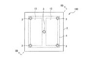
第1実施形態に係る発光装置の構成について、図1A〜図1Dを参照して説明する。
図1Aは、第1実施形態に係る発光装置の構成を示す模式的平面図である。図1Bは、第1実施形態に係る発光装置の構成を示す模式的断面図であり、図1AのIB−IB線における断面を示す。図1Cは、第1実施形態に係る発光装置における波長変換部材の変形例を示す模式的断面図である。図1Dは、第1実施形態に係る発光装置における波長変換部材の他の変形例の構成を示す模式的断面図である。
なお、図1A及び図1Bにおいて、発光装置100が備える半導体発光素子1について、成長基板11、半導体積層体12、n側電極13及びp側電極15以外の構成は記載を省略しており、記載した部材についても簡略化して示している。後記する図4A及び図6A〜図8、図10A〜図13、図15B〜図17についても同様である。また、図1C及び図1Dは、発光素子1の上面に設けられた波長変換部材2A,2Bの一部を拡大して示している。
First Embodiment
[Configuration of light emitting device]
The configuration of the light emitting device according to the first embodiment will be described with reference to FIGS. 1A to 1D.
FIG. 1A is a schematic plan view showing the configuration of the light emitting device according to the first embodiment. FIG. 1B is a schematic cross-sectional view showing the configuration of the light emitting device according to the first embodiment, and shows a cross section taken along line IB-IB in FIG. 1A. FIG. 1C is a schematic cross-sectional view showing a modification of the wavelength conversion member in the light emitting device according to the first embodiment. FIG. 1D is a schematic cross-sectional view showing the configuration of another modification of the wavelength conversion member in the light emitting device according to the first embodiment.
1A and 1B, the configuration of the semiconductor
第1実施形態に係る発光装置100は、フリップチップ型の半導体発光素子1(以下、適宜「発光素子」と呼ぶ)と、発光素子1の上面に設けられる波長変換部材2及び支持部材3と、発光素子1の側面に設けられる光反射部材4と、を備えて構成されている。発光装置100は、導電接着剤を用いた実装の際に上方から印加される荷重を支持部材3によって受け、当該荷重が波長変換部材2に作用しないように実装面であるn側電極13及びp側電極15の下面に伝達するように構成されている。これによって、発光装置100は、波長変換部材2に損傷を与えることなく導電接着剤を用いた実装が可能となる。
また、第1実施形態に係る発光装置100は、CSP(Chip Size Package又はChip Scale Package)型の発光装置である。
The
The
次に、発光装置100の各部の構成について順次に詳細に説明する。
発光素子1は、平面視で略正方形である略四角柱形状を有しており、n側電極13及びp側電極15が一方の面側に設けられるとともに、フリップチップ実装に適した構成を有するLEDチップである。
ここで、発光素子1の構成例について、図2を参照して説明する。
図2は、第1実施形態に係る発光装置における半導体発光素子の構成例を示す模式的断面図である。
なお、図2においては、n側電極13及びp側電極15が設けられた面が上方となるように示しており、図1Bとは上下を逆に示している。
Next, the configuration of each part of the
The
Here, a configuration example of the
FIG. 2 is a schematic cross-sectional view showing a configuration example of a semiconductor light emitting element in the light emitting device according to the first embodiment.
In addition, in FIG. 2, it has shown so that the surface in which the
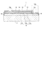
発光素子1は、成長基板11と、半導体積層体12と、n側電極13と、全面電極14と、p側電極15と、絶縁膜16とを備えている。
発光素子1は、成長基板11の一方の面上に、n型半導体層12nとp型半導体層12pとを積層した半導体積層体12を備えている。半導体積層体12は、n側電極13及びp側電極15間に外部電源を接続して通電することにより発光するようになっており、n型半導体層12nとp型半導体層12pとの間に活性層12aを備えることが好ましい。
The
The
成長基板11は、半導体積層体12をエピタキシャル成長させるための基板である。成長基板11は、半導体積層体12をエピタキシャル成長させることができる基板材料で形成されればよく、大きさや厚さ等は特に限定されない。例えば、半導体積層体12をGaN(窒化ガリウム)などの窒化物半導体を用いて形成する場合には、基板材料としては、C面、R面、A面の何れかを主面とするサファイアやスピネル(MgAl2O4)のような絶縁性基板、また炭化ケイ素(SiC)、ZnS、ZnO、Si、GaAs、ダイヤモンド、及び窒化物半導体と格子接合するニオブ酸リチウム、ガリウム酸ネオジム等の酸化物基板が挙げられる。なお、発光素子1をフリップチップ実装に適した構成とするためには、成長基板11は、良好な透光性を有する材料を用いることが好ましい。
The
半導体積層体12は、活性層12aを含むn型半導体層12nとp型半導体層12pとが積層された積層体である。半導体積層体12には、p型半導体層12p及び活性層12aが部分的に存在しない領域、すなわちp型半導体層12pの表面から凹んだ領域(この領域を「段差部12b」と呼ぶ)が形成されている。段差部12bの底面には、n型半導体層12nと電気的に接続されたn側電極13が設けられている。p型半導体層12pの上面の略全面には、良好な導電性と光反射性とを有する全面電極14が設けられている。また、半導体積層体12の表面は、段差部12bの底面の一部及び全面電極14の上面の一部を除き、直接に又は全面電極14を介して、絶縁膜16によって被覆されている。
The
半導体積層体12(n型半導体層12n、活性層12a及びp型半導体層12p)は、InXAlYGa1−X−YN(0≦X、0≦Y、X+Y<1)等が好適に用いられる。また、これらの半導体層は、それぞれ単層構造でもよいが、組成及び膜厚等の異なる層の積層構造、超格子構造等であってもよい。特に、活性層12aは、量子効果が生ずる薄膜を積層した単一量子井戸又は多重量子井戸構造であることが好ましい。
The semiconductor laminate 12 (n-
全面電極14は、p型半導体層12pの上面の略全面を覆うように設けられる。全面電極14は、上面の一部に設けられたp側電極15を介して供給される電流を、p型半導体層12pの全面に拡散させるための導体層である。また、全面電極14は良好な光反射性を有し、発光素子1が発光する光を、光取り出し面である下方向(図1Bにおいては上方向)に反射させる光反射膜としても機能する。
The
全面電極14は、良好な導電性と光反射性とを有する金属材料を用いることができる。特に可視光領域で良好な光反射性を有する金属材料としては、Ag、Al又はこれらの金属を主成分とする合金を好適に用いることができる。また、全面電極14は、これらの金属材料を単層で、又は積層したものが利用できる。特に全面電極14の下層(p型半導体層12p側)としてマイグレーションしやすいAgを用いる場合には、上層として、例えば、Al、Ti、W、Auなどのような良好な導電性とバリア性とを有する金属材料を用いて、当該下層を被覆することが好ましい。
The
n側電極13は、半導体積層体12の段差部12bの底面において、絶縁膜16の開口部16n内でn型半導体層12nと電気的に接続されるように設けられている。また、p側電極15は、全面電極14の上面において、絶縁膜16の開口部16p内で全面電極14と電気的に接続されるように設けられている。n側電極13はn型半導体層12nに、p側電極15は全面電極14を介してp型半導体層12pに、外部からの電流を供給するためのパッド電極である。
また、n側電極13及びp側電極15は、絶縁膜16を介して、全面電極14上の広範囲に延在するように設けられている。
The n-
Further, the n-
n側電極13及びp側電極15としては、金属材料を用いることができ、例えば、Ag、Al、Ni、Rh、Au、Cu、Ti、Pt、Pd、Mo、Cr、Wなどの単体金属及びそれらの合金などを好適に用いることができる。また、n側電極13及びp側電極15は、これらの金属材料を単層で、又は積層したものを利用することができる。
A metal material can be used as the n-
絶縁膜16は、半導体積層体12及び全面電極14の上面及び側面を被覆する層であり、発光素子1の保護膜として機能する。絶縁膜16は、段差部12bの底面の一部に開口部16nを有し、全面電極14の上面の一部に開口部16pを有している。また、絶縁膜16の上面の広範囲には、n側電極13及びp側電極15が相補的に延在するように設けられている。
絶縁膜16としては、金属酸化物や金属窒化物を用いることができ、例えば、Si、Ti、Zr、Nb、Ta、Alからなる群より選択された少なくとも一種の金属の酸化物又は窒化物を好適に用いることができる。
The insulating
As the insulating
なお、図2に示した発光素子1は、一例を示しものであり、外形形状や、段差部12b、n側電極13及びp側電極15の配置領域などは適宜に変更することが可能である。
The
図1A及び図1Bに戻って、発光装置100の構成について説明を続ける。
波長変換部材2は、発光素子1の光取り出し面である上面側に設けられており、発光素子1が発する光を異なる波長の光に変換する波長変換物質の粒子21を含有する層である。
波長変換物質とは具体的には蛍光体であり、波長変換部材2は、蛍光体の粒子を含有した透光性の樹脂22を用いて形成することができる。
また、発光素子1の上面には、波長変換部材2を厚さ方向に貫通するように、複数の支持部材3が配置されている。支持部材3は略球形の粒子であり、下端が発光素子1の上面と接するとともに、上端が波長変換部材2の上面から露出するように設けられている。
Referring back to FIGS. 1A and 1B, the description of the configuration of the
The
Specifically, the wavelength conversion material is a phosphor, and the
Further, a plurality of
波長変換部材2に用いる樹脂22の材料としては、良好な透光性を有することが好ましい。また、樹脂材料として熱硬化性樹脂を用いることが好ましい。溶剤に熱硬化性樹脂と波長変換物質の固形粒子とを含有するスラリーを処方して、スプレー塗布した後に加熱することにより熱硬化性樹脂を硬化させる。これによって、光反射性物質の固形粒子を高含有率で含有させた場合でも、安定した膜厚で波長変換部材2を形成することができる。
The material of the
このような樹脂材料としては、例えば、シリコーン樹脂、シリコーン変性樹脂、エポキシ樹脂、エポキシ変性樹脂、ユリア樹脂、フェノール樹脂、ポリカーボネート樹脂、アクリル樹脂、ポリメチルペンテン樹脂、ポリノルボルネン樹脂、又はこれらの樹脂を1種類以上含むハイブリッド樹脂などが挙げられる。なかでも、シリコーン樹脂又はエポキシ樹脂が好ましく、特に耐光性及び耐熱性に優れるシリコーン樹脂がより好ましい。 As such a resin material, for example, silicone resin, silicone modified resin, epoxy resin, epoxy modified resin, urea resin, urea resin, phenol resin, polycarbonate resin, acrylic resin, polymethylpentene resin, polynorbornene resin, or these resins The hybrid resin etc. which contain 1 or more types are mentioned. Among them, silicone resins or epoxy resins are preferable, and in particular, silicone resins excellent in light resistance and heat resistance are more preferable.
また、波長変換部材2は、スプレー法の他に、金型を用いた成形法、スクリーン印刷法などの各種印刷法により形成することもできる。波長変換部材2を形成する際に、粘度や流動性を調整するために、前記したスラリーにシリカの粒子などを添加するようにしてもよい。
Moreover, the
波長変換部材2の膜厚は、蛍光体の含有量や、発光素子1が発光する光と波長変換後の光との混色後の色調などによって定めることができ、例えば、1μm以上1000μm以下とすることができ、5μm以上500μm以下が好ましく、10μm以上200μm以下がより好ましい。
The film thickness of the
本実施形態において、波長変換部材2は、光反射部材4の上面にまで延在するように設けられているが、発光素子1上にのみ設けるようにしてもよい。また、光反射部材4に代えて、発光素子1の側面にも設けるようにしてもよい。更にまた、発光素子1の側面に波長変換部材2を設け、更にその外側に光反射部材4を設けるようにしてもよい。
In the present embodiment, the
また、蛍光体(波長変換物質の粒子21)としては、発光素子1が発する波長の光によって励起されて、この励起光と異なる波長の蛍光を発する蛍光物質であれば特に限定されず、粒状の蛍光体を好適に用いることができる。粒状の蛍光体は、光散乱性及び光反射性を有するため、波長変換機能に加えて光散乱部材としても機能し、光の拡散効果を得ることができる。蛍光体は、当該蛍光体が含有される樹脂層中に一様に分散されていることが好ましい。
The phosphor (
また、スプレー法によって波長変換部材2を形成する場合は、蛍光体は、溶剤及び熱硬化性樹脂とともに処方されるスラリーがスプレー塗布可能なように、平均粒径が2.5〜30μm程度とすることが好ましい。
なお、蛍光体の平均粒径の値は、空気透過法又はF.S.S.S.No(Fisher−SubSieve−Sizers−No.)によるものとする(いわゆるDバー(Dの上にバー)で表される値)。
When the
In addition, the value of the average particle diameter of fluorescent substance is an air permeation method or F.I. S. S. S. No (Fisher-SubSieve-Sizers-No.) (The value represented by the so-called D bar (the bar above D)).
蛍光体材料としては、当該分野で公知のものを使用することができる。例えば、緑〜黄色に発光するセリウムで賦活されたYAG(イットリウム・アルミニウム・ガーネット)系蛍光体、緑色に発光するセリウムで賦活されたLAG(ルテチウム・アルミニウム・ガーネット)系蛍光体、緑〜赤色に発光するユーロピウム及び/又はクロムで賦活された窒素含有アルミノ珪酸カルシウム(CaO−Al2O3−SiO2)系蛍光体、青〜赤色に発光するユーロピウムで賦活されたシリケート((Sr,Ba)2SiO4)系蛍光体、緑色に発光するβサイアロン蛍光体、赤色に発光するCASN系又はSCASN系蛍光体などの窒化物系蛍光体、赤色に発光するKSF(K2SiF6:Mn)系蛍光体、緑色又は赤色に発光する硫化物系蛍光体などが挙げられる。 As the phosphor material, those known in the art can be used. For example, YAG (yttrium aluminum garnet) phosphor activated with cerium emitting green to yellow, LAG (lutetium aluminum garnet) phosphor activated with cerium emitting green, to green to red Nitrogen-containing calcium aluminosilicate (CaO-Al 2 O 3 -SiO 2 ) phosphor activated with europium and / or chromium that emits light, europium-activated silicate ((Sr, Ba) 2 that emits blue to red light SiO 4 ) -based phosphor, β-sialon phosphor emitting green light, nitride-based phosphor such as CASN-based or SCASN-based phosphor emitting red, KSF (K 2 SiF 6 : Mn) -based phosphor emitting red And sulfide-based phosphors that emit green or red light.
また蛍光体材料は、例えば、いわゆるナノクリスタル、量子ドットと称される発光物質でもよい。このような材料としては、半導体材料、例えば、II−VI族、III−V族、IV−VI族、I−III−VI族の半導体、具体的には、CdSe、コアシェル型のCdSXSe1−X/ZnS、GaP、InAs、InP、GaN、PbS、PbSe、Cu(In,Ga)S2、Ag(In,Ga)S2等のナノサイズの高分散粒子を挙げることができる。このような蛍光体は、例えば、粒径1〜100nm、好ましくは1〜20nm程度(原子が10〜50個程度)とすることができる。このような粒径の蛍光体を用いることにより、内部散乱を抑制することができ、色変換された光の散乱を抑制し、波長変換部材2の光の透過率をより一層向上させることができる。
The phosphor material may be, for example, a so-called nanocrystal or a luminescent material called a quantum dot. Such materials include semiconductor materials, for example, semiconductors of II-VI, III-V, IV-VI, I-III-VI, specifically CdSe, core-shell type CdS X Se 1 -X / ZnS, may be mentioned GaP, InAs, InP, GaN, PbS, PbSe, Cu (in, Ga)
支持部材3は、下端が発光素子1の上面と接するように、当該上面の複数の箇所に設けられており、発光装置100の実装時に、上方から印加される荷重を受け、当該荷重を波長変換部材2に作用させることなく、発光素子1の実装面であるn側電極13及びp側電極15の下面に伝達させるための部材である。また、支持部材3の上端は、波長変換部材2の上面と同じ高さか、当該上面よりも高くなるような粒径を有している。
複数の支持部材3は、粒径及び形状の均一性が高く、かつ発光素子1の上面に均等に配置されている。支持部材3の粒径及び形状を均一とすることで、複数の支持部材3の高さが揃い、発光装置100の実装時に複数の支持部材3がプレスヘッドからの荷重を均等に受けることができる。
The
The plurality of
なお、ここで、「高さ」とは、発光素子1の成長基板11の半導体積層体12が設けられた一方の面と、当該一方の面と反対側の面である他方の面とに垂直な方向を高さ方向とし、他方の面が一方の面よりも高い位置であるとする。すなわち、成長基板11の他方の面からの垂直方向の距離が離れるほど、「高い」ことを意味する。
また、「均等に配置する」とは、一定の面積内に配置される個数が著しく偏らないように配置されることをいうものとする。従って、複数の支持部材3は、一定の間隔で規則的に配置されてもよく、ランダムな間隔で配置されてもよい。
Here, the “height” is perpendicular to one surface of the
Also, "evenly arranged" means arranged so that the number arranged in a certain area is not significantly deviated. Therefore, the plurality of
具体的には、発光素子1の平面視形状が矩形状である場合は、支持部材3は、平面視で略矩形形状である発光素子1の上面の4隅に配置することが好ましく、更に中央に配置されることがより好ましい。複数の支持部材3を均等な間隔で配置することで、上方から印加される荷重を発光素子1の上面全体に均等に伝達することができる。このため、発光素子1が局所的に荷重されることでダメージを受けることを防止することができる。また、実装面に均等に圧力が加えられるため、発光素子1の実装面全体が導電性粒子81によって偏りなく実装基板と電気的に接続される。
Specifically, when the plan view shape of the
なお、支持部材3の配置数は5個に限定されるものではないが、荷重を広い領域に伝達できるように、少なくとも3個が同一直線上とならない配置で設けられることが好ましい。また、3個以上の支持部材3を、発光素子1の上面の、平面視で外縁の近傍に互いに間隔を開けて配置することが好ましい。また、更に多数の支持部材3を配置する場合は、支持部材3を発光素子1の上面の全体にランダムに散布することで配置してもよい。
In addition, although the arrangement number of the supporting
支持部材3の粒径は、波長変換部材2の膜厚に応じて、好適には、波長変換部材2の膜厚と同じか、好ましくは当該膜厚よりも大きくなるように定めることができる。特に波長変換物質の粒子21へのダメージを防止するという観点からは、支持部材3の上端が波長変換部材2中の波長変換物質の粒子21の最上端以上で、かつ、支持部材3の下端が波長変換部材2中の波長変換物質の粒子21の最下端以下とすることが好ましい。また、支持部材3は、剛性が波長変換部材2よりも高いか同じであることが好ましい。これによって、支持部材3が荷重を受けて変形しても、波長変換部材2に大きな負荷がかからないように、荷重を発光素子1に伝達することができる。
なお、実装時に波長変換部材2が、上方からの荷重によって塑性変形しない範囲であれば、波長変換部材2に荷重が作用してもよい。従って、支持部材3の粒径(高さ)は、波長変換部材2の厚さより20%程度低くてもよい。すなわち、支持部材3の粒径は、波長変換部材2の厚さの0.8倍以上程度であればよい。
The particle diameter of the
A load may be applied to the
支持部材3は、良好な透光性を有するか、表面に良好な光反射性を有することが好ましい。これによって、波長変換部材2の内部を伝播する光が支持部材3によって吸収されることが抑制され、結果として外部への光取り出し効率の低下を防止することができる。
支持部材3は、このような材料として、透光性を有する樹脂材料、シリカなどの透光性を有する無機材料、光反射性の良好な金属材料などを用いることができる。
また、支持部材3としては、例えば、液晶表示装置において、基板間の厚さを一定に保つために用いられているスペーサビーズと同様のものを用いることができる。
It is preferable that the
The supporting
Further, as the supporting
支持部材3としては、更に具体的には、ガラス、SiO2、Al2O3、希土類などのセラミックスのフィラーや柱状、壁状などの構造体、LCP(液晶ポリマー樹脂)、PPA(ポリフタルアミド樹脂)などのエンジニアリングプラスチックや熱硬化性樹脂などの透明部材もしくはこれらの樹脂コアに金属反射膜をコーティングした高反射性樹脂フィラーや構造体など、を挙げることができる。また、支持部材3として、金属のフィラーや構造体、カーボンのフィラーや構造体なども用いることができる。実装時の荷重によって塑性変形せずに、変形後に復元した寸法が揃った粒子や構造体であれば、支持部材3として用いることができる。
More specifically, the
また、支持部材3を発光素子1の上面に形成する場合は、サファイアや易研削性を有する酸化物材料などを、エッチングや研削加工することで、支持部材3として構造体を形成することができる。また、各種の金属、無機材料、有機材料を、半導体製造の手法、スパッタ法、蒸着法、スピンコート法などの塗布法で形成し、パターニングして用いるようにしてもよい。更にまた、圧縮成形法、トランスファー成形法などの成形手法を用いて支持部材3を形成することもできる。
In addition, when the
なお、支持部材3が透光性を有する材料で構成される場合は、発光素子1からの光が、支持部材3を介して波長変換されずに外部に取り出される。このため、支持部材3の径が大きくなるほど、発光装置100の配光特性に色むらが生じ易くなる。従って、色むらが目立たないように、支持部材3の径は、波長変換部材2の厚さの1.5倍以下程度とすることが好ましい。
また、平面視において、複数の支持部材3の面積の合計は、発光素子1の発光部であるp型半導体層12pが配置される面積の30%以下程度とすることが好ましい。これによって、色むらを目立たない範囲とするとともに、波長変換部材2によって適切に波長変換することができる。
In addition, when the
Further, in plan view, the total area of the plurality of
また、支持部材3は、上端が、波長変換部材の上面よりも低くなるような大きさとすることもできる。波長変換部材は、波長変換物質の粒子21を含有させた樹脂22を発光素子1の上面に塗布することなどにより形成されるが、樹脂22が硬化するまでの間に、相対的に比重の大きな波長変換物質の粒子21が沈降することがある。
このようにして形成された波長変換部材2Aは、図1Cに示すように、波長変換物質の粒子21を含有する領域である粒子含有部2aと、波長変換物質の粒子21を含有しない樹脂22のみの領域である粒子非含有部2bとの2層構成となる。
The
The
なお、粒子含有部2aは、波長変換部材2が設けられる発光素子1の上面の高さから、複数の波長変換物質の粒子21の最上端の高さまでの領域のことである。また、波長変換部材2Aが、波長変換物質以外の、例えば、光拡散性の粒子などのフィラーを含有する場合は、これらのフィラーも含めた粒子の最上端までの領域を粒子含有部2aとする。また、粒子非含有部2bは、波長変換部材2の粒子含有部2aよりも上側の領域のことである。但し、他のフィラーが、波長変換物質の粒子よりも粒径が小さかったり、形状が球形に近いなど、当該フィラーを含有する樹脂部が、波長変換物質の粒子を含有する樹脂部よりも塑性変形し難い場合は、当該他のフィラーを含有していても、波長変換物質の粒子を含有しない樹脂部は、粒子非含有部2bとして取り扱うようにしてもよい。
The particle-containing
また、波長変換部材2Aを、発光素子1の側面にも設けるようにしてもよいが、この場合は波長変換部材2Aの当該側面に設けられた箇所には支持部材3を設けないようにし、、波長変換部材2Aの剥離を防止する。従って、支持部材3の下端は、波長変換部材2Aの発光素子1の上面に設けられた箇所についての下端以下の高さとなるようにすればよい。
In addition, the
波長変換物質の粒子21を含有しないことで、粒子非含有部2bは、上方から荷重を受けた場合に、粒子含有部2aよりも塑性変形し難くなる。このため、粒子含有部2aに作用する荷重を軽減するために、支持部材3は、その上端が、粒子含有部2aの上端以上の高さとなるように設けることができる。これによって、波長変換部材2Aの上面に荷重が印加されても、波長変換物質の粒子21へ荷重の作用が低減され、波長変換部材2Aに対する実質的なダメージを防止することができる。
なお、波長変換部材2Aに対するダメージの恐れをより低減するために、支持部材3の上端が、粒子非含有部2bの上端以上の高さ、すなわち波長変換部材2Aの上面以上の高さとなるように設けるようにしてもよい。
By not containing the
In order to further reduce the risk of damage to the
なお、後記する変形例や他の実施形態においても、波長変換部材2に代えて、2層構成の波長変換部材2Aを用いるようにしてもよい。その場合は、支持部材3の上端が、粒子含有部2aの上端以上の高さとなるように設けることができる。
Also in the modification described later and other embodiments, the
また、前記したように、上方からの荷重によって波長変換部材2が塑性変形しない範囲であれば、支持部材3の高さは、波長変換部材2の膜厚の0.8倍以上程度であればよい。特に、図1Dの上段側に示すように、波長変換部材2Bが含有する波長変換物質の粒子21が、波長変換部材2B中に疎らに分散している場合は、波長変換部材2Bの膜厚に対して、支持部材3の高さを、より低くすることができる。図1Dの下段側に示すように、実装時の上方からの荷重によって、波長変換部材2Bが圧縮変形しても、波長変換物質の粒子21が支持部材3の高さの範囲内に逃げることができるため、波長変換物質の粒子21に大きな荷重が掛からずに、実質的に波長変換部材2Bへのダメージを避けることができる。
Further, as described above, if the
光反射部材4は、発光素子1の側面を被覆するように設けられ、発光素子1の側面から出射する光を発光素子1内に反射させる部材である。ここで、光反射部材4は、光が伝播する部材である半導体積層体12及び成長基板11の側面に設けられる。これによって、光取り出し面である発光素子1の上面の発光輝度を向上させることができる。
また、光反射部材4は、発光素子1のn側電極13及びp側電極15の下面を除き、発光素子1の下面も被覆するように設けられている。
The
The
光反射部材4は、透光性を有する樹脂に、光反射性物質の粒子を含有させた白色の樹脂層として形成することができるが、これに限定されるものはない。光反射部材4として、誘電体多層膜からなるDBR(分布ブラッグ反射鏡)膜を設けてもよく、外側又は中間層として金属膜を含めた多層膜で構成してもよい。また、光反射性物質の含有率を変えた複数の樹脂層を積層するようにしてもよい。
また、光反射部材4は必須の構成ではない。例えば、光反射部材4に代えて、発光素子1の上面及び側面を一体的に被覆するように波長変換部材2を設けるようにしてもよい。
The
The
光反射部材4を、透光性を有する樹脂に光反射性物質の粒子を含有させて構成する場合は、樹脂材料としては、前記した波長変換部材2と同様の樹脂材料を用いることができる。
また、光反射性物質は、樹脂材料との屈折率差が大きく、良好な透光性を有する材料の粒子を用いることが好ましい。このような光反射性物質としては、屈折率が、例えば1.8以上であって、光を効率的に散乱し高い光取り出し効率を得るためには、2.0以上であることが好ましく、2.5以上であることがより好ましい。樹脂材料との屈折率差は、例えば0.4以上であって、光を効率的に散乱し高い光取り出し効率を得るためには、0.7以上であることが好ましく、0.9以上であることがより好ましい。また、光反射性物質の粒子の平均粒径は、高い効率で光散乱効果を得られるように、0.08μm以上10μm以下であることが好ましく、0.1μm以上5μm以下であることがより好ましい。
In the case where the
Further, as the light reflective substance, it is preferable to use particles of a material having a large difference in refractive index with the resin material and having a good light transmitting property. As such a light reflective substance, it is preferable that the refractive index is, for example, 1.8 or more, and in order to efficiently scatter light and obtain high light extraction efficiency, it is preferably 2.0 or more, More preferably, it is 2.5 or more. The difference in refractive index with the resin material is, for example, 0.4 or more, and in order to efficiently scatter light and obtain high light extraction efficiency, it is preferably 0.7 or more, and 0.9 or more. It is more preferable that Further, the average particle diameter of the particles of the light reflective substance is preferably 0.08 μm or more and 10 μm or less, and more preferably 0.1 μm or more and 5 μm or less so that the light scattering effect can be obtained with high efficiency. .
このような光反射性物質としては、TiO2(酸化チタン)、ZrO2(酸化ジルコニウム)、MgO(酸化マグネシウム)、MgCO3(炭酸マグネシウム)、Mg(OH)2(水酸化マグネシウム)、CaCO3(炭酸カルシウム)、Ca(OH)2(水酸化カルシウム)、CaSiO3(珪酸カルシウム)、ZnO(酸化亜鉛)、BaTiO3(チタン酸バリウム)、Al2O3(酸化アルミニウム)などを用いることができる。なかでも、TiO2は、水分などに対して比較的安定でかつ高屈折率であり、また熱伝導性にも優れるため、好ましい。
また、より良好な反射性を得るために、発光素子1が発する光が可視光の場合には、光反射性物質としてTiO2を用いることが好ましく、紫外光の場合には、光反射性物質としてAl2O3を用いることが好ましい。
As such light reflective substances, TiO 2 (titanium oxide), ZrO 2 (zirconium oxide), MgO (magnesium oxide), MgCO 3 (magnesium carbonate), Mg (OH) 2 (magnesium hydroxide), CaCO 3 (Calcium carbonate), Ca (OH) 2 (calcium hydroxide), CaSiO 3 (calcium silicate), ZnO (zinc oxide), BaTiO 3 (barium titanate), Al 2 O 3 (aluminum oxide), etc. it can. Among them, TiO 2 is preferable because it is relatively stable to moisture and the like, has a high refractive index, and is excellent in thermal conductivity.
Further, in order to obtain better reflectivity, it is preferable to use TiO 2 as the light reflecting substance when the light emitted from the
光反射部材4は、波長変換部材2の形成方法と同様に、スプレー塗布法、スクリーン印刷法やインクジェット法などの各種印刷法、金型を用いた成形方法などにより形成することができる。
The
[発光装置の実装方法]
次に、発光装置100の実装方法について、図3〜図4Bを参照して説明する。
図3は、第1実施形態に係る発光装置の実装方法の手順を示すフローチャートである。図4Aは、第1実施形態に係る発光装置の実装方法を説明するための模式的断面図である。図4Bは、第1実施形態に係る発光装置の実装に用いられる導電接着剤に含有される導電性粒子の構成を示す模式的断面図である。
[Mounting method of light emitting device]
Next, the mounting method of the
FIG. 3 is a flowchart showing the procedure of the light emitting device mounting method according to the first embodiment. FIG. 4A is a schematic cross-sectional view for explaining the mounting method of the light emitting device according to the first embodiment. FIG. 4B is a schematic cross-sectional view showing the configuration of conductive particles contained in the conductive adhesive used for mounting the light emitting device according to the first embodiment.
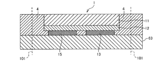
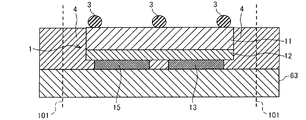
発光装置100の実装方法は、実装基板載置工程S101と、導電接着剤配置工程S102と、発光装置配置工程S103と、荷重工程S104と、硬化工程S105とが含まれている。
The mounting method of the
まず、実装基板載置工程S101において、載置台62に実装基板70を載置する。実装基板70は、基体71と、基体71の表面に発光装置100の正負の電極であるn側電極13及びp側電極15と電気的に接続するための一対の配線用電極72とを備えている。実装基板70は、配線用電極72が上側となるように載置台62に載置される。
なお、実装基板70は、基体71と配線用電極72のみを示しているが、用途に応じて基体71及び配線用電極72はそれぞれ適宜な大きさや形状のものを用いることができ、更に実装基板70に他の部品が搭載されていてもよい。
First, the mounting
Although only the
次に、導電接着剤配置工程S102において、実装基板70の配線用電極72上に、発光装置100を接合するために必要な適量の導電接着剤80を配置する。導電接着剤80は、樹脂82に導電性粒子81を分散してなる接着剤であり、実装時に上方から荷重を印加(加圧)することによって、発光装置100と実装基板70とを接合するものである。特に狭間隔で電極が設けられている場合は、異方性導電接着剤を好適に用いることができる。また、導電接着剤80は、例えば、ACP(異方性導電ペースト)やACF(異方性導電フィルム)のように、ペースト状又はフィルム状の何れの形態のものでも用いることができる。
Next, in the conductive adhesive arranging step S102, an appropriate amount of the conductive adhesive 80 necessary for bonding the
異方性を有する導電接着剤80は、実装基板70の配線用電極72と発光装置100のn側電極13及びp側電極15との間を導電性粒子81によって縦方向(実装面に垂直な方向)に電気的に接続するとともに、横方向(実装面に平行な方向)には、導電性粒子81同士が互いに連続して接触しないように、適度な量の導電性粒子81が樹脂82に分散されている。
The conductive adhesive 80 having anisotropy is vertically oriented (perpendicular to the mounting surface) by the
導電性粒子81は、球形状で弾性を有する樹脂コア81aと、当該樹脂コア81aの表面を被覆する金属層81bとから構成される。導電性粒子81はこれに限定されるものではなく、他の構成を有するものであってもよい。
また、樹脂82は、熱硬化性樹脂、紫外線硬化樹脂、熱可塑性樹脂など、配置時に流動性を有し、加熱、紫外線照射又は冷却などにより硬化させることができる樹脂材料を用いることができる。以下、説明の便宜上、特に断らない限り、樹脂82は熱硬化性樹脂からなるものとして説明する。
The
Further, as the
また、導電接着剤80としては、上方から荷重を印加(加圧)して接合するものであれば、他の構成のものでも用いることができる。また、導電接着剤80として、異方性を有さないものでも用いることができる。
導電接着剤としては、前記したACP,ACFの他に、例えば、CuコアがSnやAuSnなどの半田で被覆された構造を有する再溶融抑制半田粒子を含有した導電接着剤、Sn−Bi系、Sn−In系、Sn−Zn系、Sn−Ag−In系、Sn−Zn−Bi系などの低融点半田粒子を含有した導電接着剤を挙げることができ、約180〜250℃の比較的に低温で接合することができる。また、これらの導電性粒子を含有する導電接着剤を用いた接合の際に必要な荷重は、約0.1〜10N/mm2程度であり、0.1〜2N/mm2程度で接合可能なものがより好ましい。
In addition, as the
As the conductive adhesive, for example, a conductive adhesive containing a remelting inhibiting solder particle having a structure in which a Cu core is covered with a solder such as Sn or AuSn, in addition to the above-described ACP and ACF, Sn-Bi-based, A conductive adhesive containing low melting point solder particles such as Sn-In, Sn-Zn, Sn-Ag-In, Sn-Zn-Bi, etc. can be mentioned, and it is relatively about 180 to 250 ° C. It can be joined at low temperature. In addition, the load necessary for bonding using a conductive adhesive containing these conductive particles is about 0.1 to 10 N / mm 2 or so, and bonding is possible on the order of 0.1 to 2 N / mm 2 Are more preferred.
また、導電接着剤に含有させる導電性粒子は、前記したようにコアが樹脂の場合を含めて、次のような組み合わせのものを用いることができる。すなわち、導電性粒子として、金属被覆樹脂コア、半田被覆樹脂コア、金属被覆金属コア、半田被覆金属コア、金属被覆カーボンコア、半田被覆カーボンコアなどを用いることができる。 The conductive particles to be contained in the conductive adhesive can be used in the following combination, including the case where the core is a resin as described above. That is, as the conductive particles, a metal-coated resin core, a solder-coated resin core, a metal-coated metal core, a solder-coated metal core, a metal-coated carbon core, a solder-coated carbon core, etc. can be used.
次に、発光装置配置工程S103において、実装基板70の配線用電極72上に、導電接着剤80を介して発光装置100を配置する。発光装置100は、実装面であるn側電極13及びp側電極15の下面が、それぞれ対応する極性の配線用電極72と対向するように配置する。
Next, in the light emitting device disposing step S103, the
次に、荷重工程S104において、発光装置100の上面にプレスヘッド61を押し当て、所定の力で荷重する。このとき、プレスヘッド61の下面は発光装置100の支持部材3の上端部と接し、荷重は支持部材3で受ける。そして、プレスヘッド61から受ける荷重は、支持部材3を介して、成長基板11及び半導体積層体12を経由して発光装置100の実装面であるn側電極13及びp側電極15の下面側に伝達される。従って、波長変換部材2にはプレスヘッド61から受ける荷重が作用しないため、当該荷重により波長変換部材2が損傷しないように構成されている。
Next, in a loading step S104, the
また、プレスヘッド61から荷重を受けることにより、n側電極13及びp側電極15と、配線用電極72との間に配置された導電接着剤80に含有される導電性粒子81が押し潰されるように変形することで、n側電極13及びp側電極15と、それぞれが対応する極性の配線用電極72との間が電気的に接続される。
Further, by receiving a load from the
次に、硬化工程S105において、プレスヘッド61によって荷重された状態を維持したまま、導電接着剤80の樹脂82を硬化させる。樹脂82が熱硬化性樹脂である場合は、例えば載置台62及びプレスヘッド61にヒータなどの加熱手段を設けておき、当該加熱手段を用いて加熱することで樹脂82を硬化させることができる。
導電接着剤80の樹脂82が硬化した後に、プレスヘッド61による荷重を解放することで、実装基板70に発光装置100が実装された装置、例えば光源装置200を取り出すことができる。
Next, in the curing step S105, the
After the
なお、加熱手段は、発光装置100の下方側である載置台62のみに設けるようにしてもよい。発光装置100の下側からのみ加熱されることで、発光装置100の上部である波長変換部材2の温度を比較的低温に保つことができる。そのため、波長変換部材2を構成する波長変換物質(蛍光体)の粒子21や樹脂22として、耐熱性がより低い材料であっても用いることができる。
The heating means may be provided only on the mounting table 62 which is the lower side of the
また、導電接着剤80の樹脂82が紫外線硬化樹脂である場合は、前記した加熱に代えて、樹脂82に紫外線を照射することで樹脂82を硬化させることができる。
また、樹脂82が熱可塑性樹脂である場合は、導電接着剤配置工程S102において、樹脂82を加熱溶融させた導電接着剤80を実装基板70の配線用電極72上に配置し、発光装置配置工程S103で発光装置100を配置した後に、プレスヘッド61によって荷重を印加した状態で、冷却手段を用いて冷却又は放冷することで樹脂82を硬化させることができる。
When the
When the
[発光装置の製造方法]
次に、発光装置100の製造方法について、図5〜図6Fを参照して説明する。
図5は、第1実施形態に係る発光装置の製造方法の手順を示すフローチャートである。図6Aは、第1実施形態に係る発光装置の製造方法における半導体発光素子配置工程を示す模式的断面図である。図6Bは、第1実施形態に係る発光装置の製造方法における光反射部材形成工程の第1サブ工程を示す模式的断面図である。図6Cは、第1実施形態に係る発光装置の製造方法における光反射部材形成工程の第2サブ工程を示す模式的断面図である。図6Dは、第1実施形態に係る発光装置の製造方法における支持部材形成工程を示す模式的断面図である。図6Eは、第1実施形態に係る発光装置の製造方法における波長変換部材形成工程を示す模式的断面図である。図6Fは、第1実施形態に係る発光装置の製造方法における個片化工程を示す模式的断面図である。
[Method of manufacturing light emitting device]
Next, a method of manufacturing the
FIG. 5 is a flowchart showing the procedure of the method of manufacturing the light emitting device according to the first embodiment. FIG. 6A is a schematic cross-sectional view showing the semiconductor light emitting element arranging step in the method for manufacturing a light emitting device according to the first embodiment. FIG. 6B is a schematic cross-sectional view showing the first sub-step of the light reflecting member forming step in the method of manufacturing the light emitting device according to the first embodiment. FIG. 6C is a schematic cross-sectional view showing the second sub-step of the light reflecting member forming step in the method of manufacturing the light emitting device according to the first embodiment. FIG. 6D is a schematic cross-sectional view showing the supporting member forming step in the method of manufacturing the light emitting device according to the first embodiment. FIG. 6E is a schematic cross sectional view showing the wavelength conversion member forming step in the method of manufacturing the light emitting device according to the first embodiment. FIG. 6F is a schematic cross-sectional view showing the singulation step in the method for manufacturing a light emitting device according to the first embodiment.
なお、図6A〜図6Gは、図1AのIB−IB線に相当する位置における断面図である。また、発光装置100の製造は、複数の発光装置100が1次元又は2次元に配列したウエハ状態で製造されるウエハレベルプロセスによって行われる。図6A〜図6Fでは、仮想線である境界線101を用いて個々の発光装置100の区画を示している。
また、製造工程を示す図6A〜図6Fにおいて、左右の区画に配置された発光装置100を製造するための各部材については、一部のみを記載している。後記する他の実施形態の製造工程を示す図10A〜図10E、図15A〜図15Gについても同様である。
6A to 6G are cross-sectional views at a position corresponding to line IB-IB in FIG. 1A. In addition, the
Moreover, in FIG. 6A-FIG. 6F which show a manufacturing process, about each member for manufacturing the light-emitting
発光装置100の製造方法は、半導体発光素子準備工程S201と、半導体発光素子配置工程S202と、光反射部材形成工程S203と、支持部材形成工程S204と、波長変換部材形成工程S205と、個片化工程S206とが含まれている。
The method of manufacturing the
まず、半導体発光素子準備工程S201において、図2に示したような構成の、個片化された発光素子1を準備する。以下に、ウエハレベルプロセスで発光素子1を製造する工程例について説明するが、これに限定されるものではない。また、市販の発光素子1を入手することで当該半導体発光素子準備工程S201としてもよい。
First, in the semiconductor light emitting element preparation step S201, the singulated
具体的には、まず、サファイアなどからなる成長基板11上に、前記した半導体材料を用いて、n型半導体層12n、活性層12a及びp型半導体層12pを順次積層した半導体積層体12を形成する。
半導体積層体12が形成されると、半導体積層体12の表面の一部の領域について、上面側からp型半導体層12p及び活性層12aの全部、並びにn型半導体層12nの一部をエッチングにより除去してn型半導体層12nが底面に露出した段差部12bを形成する。
Specifically, first, a
When the
次に、p型半導体層12p及び活性層12aを有する発光領域となる領域には、p型半導体層12pの上面の略全面を覆うように、光反射性を有する全面電極14を形成する。
次に、n側電極13とn型半導体層12nとが接続される領域、及びp側電極15と全面電極14とが接続される領域に、開口部16n,16pを有するように、ウエハの表面全体に、例えば、スパッタリング法により、SiO2などの絶縁膜16を形成する。
次に、開口部16nから絶縁膜16の上面にかけて延在するように、パッド電極であるn側電極13を形成する。また、開口部16pから絶縁膜16の上面にかけて延在するように、パッド電極であるp側電極15を形成する。
Next, in a region to be a light emitting region having the p-
Next, the surface of the wafer is provided with
Next, the n-
以上により、ウエハ状態の発光素子1が形成される。
次に、ダイシング法、スクライブ法などにより、ウエハ状態の発光素子1を所定の分割領域で割断することにより個片化された発光素子1を作製することができる。
なお、ウエハを割断する前に、成長基板11の裏面を研磨して薄肉化するようにしてもよい。これにより、容易に割断することができる。
Thus, the
Next, by dicing the
The back surface of the
次に、半導体発光素子配置工程S202において、表面に粘着性を有するシート63上に、複数の発光素子1を、側面が露出するように互いに離間して配置する。また、発光素子1は、n側電極13及びp側電極15が設けられた面がシート63を対向するように載置する。シート63としては、例えば、半導体ウエハのダイシング用の塩化ビニルなどの樹脂からなるシートを用いることができる。
なお、シート63上に配置された発光素子1などの構成物の全体を指して、適宜にウエハと呼ぶ。
Next, in the semiconductor light emitting element disposing step S202, the plurality of
Note that the entire components such as the
次に、光反射部材形成工程S203において、発光素子1の側面を被覆するように、光反射部材4を形成する。この工程には2つのサブ工程が含まれる。
第1サブ工程において、ウエハの表面全体に光反射部材4となる光反射性物質を含有する樹脂層を形成する。第1サブ工程では、光反射部材4を、発光素子1の上面と同じ高さか、当該上面よりも高くなる厚さで形成する。
当該樹脂層の形成方法としては、溶剤に樹脂と光反射性物質とを含有させたスラリーを塗布する、スプレー法、インクジェット法、ポッティング法、スクリーン印刷法などの各種の塗布方法、又は金型を用いた成形方法を用いることができる。
Next, in the light reflecting member forming step S203, the
In the first sub-step, a resin layer containing a light reflecting material to be the
As a method of forming the resin layer, various coating methods such as a spray method, an ink jet method, a potting method, a screen printing method or the like, which apply a slurry containing a resin and a light reflective substance in a solvent The molding method used can be used.
第2サブ工程において、発光素子1の上面の高さに定められた切削線102まで、例えば切削装置を用いて、光反射部材4の上層部を除去する。これにより、発光素子1の光取り出し面である成長基板11の上面が露出するとともに、光反射部材4が、発光素子1の側面を被覆するようにパターニングされる。
なお、第1サブ工程において、光反射部材4を、発光素子1の上面と同じ高さで形成した場合は、第2サブ工程を省略することができる。
In the second sub-step, the upper layer portion of the
When the
次に、支持部材形成工程S204において、発光素子1の上面に、複数の支持部材3を形成する。複数の支持部材3は、平面視で互いに離間して、発光素子1の上面全体に均等に配置する。1個の発光素子1当たりに多数の支持部材3を配置する場合は、粒子の散布装置を用いて支持部材3を発光素子1の上面に配置することもできる。
なお、支持部材3は、光反射部材4上には配置しないことが好ましい。これによって、発光装置100の実装時に支持部材3が受ける荷重により、光反射部材4が発光素子1の側面から剥離することを防止することができる。
Next, in the support member forming step S204, the plurality of
Preferably, the
次に、波長変換部材形成工程S205において、発光素子1の上面及び光反射部材4の上面に、波長変換部材2を形成する。波長変換部材2は、支持部材3の高さと同じか、上面から支持部材3の上端部が露出する高さで形成する。
波長変換部材2は、前記した光反射部材4の形成方法と同様の方法で形成することができる。例えば、スプレー装置を用いて、溶剤に熱硬化性樹脂と波長変換物質(蛍光体)の粒子とを含有させたスラリーのスプレーを噴射して塗布膜を形成することで波長変換部材2を形成することができる。波長変換部材2の形成方法としては、スプレーをパルス状に、すなわち間欠的に噴射させる塗布法であるパルススプレー法が、より高精度な膜厚で塗布膜を形成できるため、好ましい。
Next, in the wavelength conversion member forming step S <b> 205, the
The
なお、支持部材形成工程S204は、波長変換部材形成工程S205の後に行うことも、同時に行うこともできる。例えば、波長変換部材形成工程S205において、波長変換部材2を形成した後であって、樹脂22が流動性を有する状態で支持部材3を配置し、支持部材3が発光素子1の上面と接するまで沈降させてから波長変換部材2の樹脂22を硬化させることで、支持部材3と波長変換部材2とを形成することができる。
また、波長変換部材形成工程S205において、樹脂及び波長変換物質の粒子に加えて、支持部材3となる粒子を含有したスラリーを調製し、当該スラリーを発光素子1の上面に塗布することで、波長変換部材2と支持部材3とを同時に形成することができる。
The support member forming step S204 can be performed after the wavelength conversion member forming step S205 or simultaneously. For example, after the
Further, in the wavelength conversion member forming step S205, a slurry containing particles to be the
更にまた、支持部材3として、波長変換部材2の膜厚と同じか、当該膜厚よりも大きな粒径を有する波長変換物質の粒子を用いるようにしてもよい。すなわち、波長変換部材2の膜厚よりも小さな粒径の波長変換物質の粒子に加えて、前記した支持部材3として適した大きさ及び形状の波長変換物質の粒子を用いて、波長変換部材2を形成するようにしてもよい。
Furthermore, as the
支持部材3として透光性材料を用いる場合は、支持部材3の内部を介して、発光素子1からの光が波長変換されずに外部に取り出されることがある。このため、支持部材3の粒径が大きくなるほど、発光装置100の配光特性に色むらが生じ易くなる。支持部材3として波長変換物質を用いることで、このような色むらの発生を抑制することができる。
When a translucent material is used as the
次に、個片化工程S206において、境界線101に沿って波長変換部材2及び光反射部材4を、ダイシング法やスクライブ法などによって切断することにより、発光装置100が個片化される。
以上の工程により、発光装置100が形成される。
Next, in the singulation step S206, the
The
<変形例>
次に、第1実施形態の変形例に係る発光装置ついて、図7A及び図7Bを参照して説明する。
図7Aは、第1実施形態の第1変形例に係る発光装置の構成を示す模式的断面図である。図7Bは、第1実施形態の第2変形例に係る発光装置の構成を示す模式的断面図である。
なお、第1変形例に係る発光装置100A及び第2変形例に係る発光装置100Bの平面視の形状は、第1実施形態に係る発光装置100と同様であり、図7A及び図7Bは、図1AのIB−IB線に相当する位置における断面を示している。
<Modification>
Next, a light emitting device according to a modification of the first embodiment will be described with reference to FIGS. 7A and 7B.
FIG. 7A is a schematic cross-sectional view showing a configuration of a light emitting device according to a first modified example of the first embodiment. FIG. 7B is a schematic cross-sectional view showing a configuration of a light emitting device according to a second modified example of the first embodiment.
The shapes of the
第1変形例に係る発光装置100Aは、発光装置100の球形状の粒子である支持部材3に代えて、円錐台形状の支柱である支持部材3Aを備えるものである。
なお、支持部材3Aは円錐台形状に限定されるものではなく、底面形状を楕円、多角形などとする錐台形状とすることができる。また、支持部材3Aは、円柱や角柱などの柱状の支柱であってもよい。更にまた、支持部材3Aは、平面視で直線状やL字状、C字状などの壁形状であってもよく、円筒や四角筒などの筒状の壁形状であってもよい。支持部材3Aを筒状とする場合は、平面視で、筒形状の中心と発光素子1の中心とが略一致するように配置することが好ましい。
また、支持部材3Aは、円柱形状を有し、当該円柱の側面が発光素子1の上面と接するように配置されてもよい。この場合は、支持部材3の高さは、円柱の底面の直径で定められる。また、支持部材3Aは、上端が平面でなく、丸味を帯びた形状、例えば半球形状であってもよい。
なお、発光素子1の上面に配置される複数の支持部材3Aは、何れの形状であっても高さが均一であることが好ましい。
A
The
In addition, the
The plurality of
なお、支持部材3Aは、支持部材3と同様の材料を用いて形成することができる。発光装置100Aは、発光装置100とは支持部材3Aの形状が異なるだけであり、発光装置100と同様の手順で製造することができる。
The
第2変形例に係る発光装置100Bは、支持部材3に代えて、発光素子1の成長基板11を加工して形成された支持部材3Bを備えるものである。支持部材3Bの形状は、柱状、錐台形状、半球形状、壁状、筒状などとすることができる。支持部材3Bの配置箇所は、発光装置100と同様である。
A
支持部材3Bは、成長基板11の他方の面(半導体積層体12が設けられた主面と反対側の主面)である上面をエッチングにより加工することで形成することができる。このため、第2変形例に係る発光装置100Bの製造方法としては、第1実施形態の製造方法において、支持部材形成工程S204を半導体発光素子準備工程S201の前に行うようにすることができる。すなわち、まず、他方の面側に支持部材3Bである凸部が形成された成長基板11を準備し、成長基板11の他方の面上に半導体積層体12などを形成するものである。
なお、支持部材形成工程S204を、波長変換部材形成工程S205よりも前に行えばよく、半導体発光素子準備工程S201の後に、又は、光反射部材形成工程S203の後に行うこともできる。
The
The support member formation step S204 may be performed before the wavelength conversion member formation step S205, and may be performed after the semiconductor light emitting element preparation step S201 or after the light reflection member formation step S203.
<第2実施形態>
[発光装置の構成]
次に、第2実施形態に係る発光装置の構成について、図8を参照して説明する。
図8は、第2実施形態に係る発光装置の構成を示す模式的断面図である。なお、第2実施形態に係る発光装置100Cの平面視の形状は、第1実施形態に係る発光装置100と略同じであり、図8は、図1AのIB−IB線に相当する位置における断面を示している。
Second Embodiment
[Configuration of light emitting device]
Next, the configuration of the light emitting device according to the second embodiment will be described with reference to FIG.
FIG. 8 is a schematic cross-sectional view showing the configuration of the light emitting device according to the second embodiment. The shape in plan view of the
第2実施形態に係る発光装置100Cは、発光素子1の側面に透光性部材5が設けられ、光反射部材4が、当該透光性部材5を介して、発光素子1の側面を被覆するように設けられている。このため、第1実施形態に係る発光装置100に比べて、平面視での外形がやや大きくなるように構成されている。
なお、第2実施形態に係る発光装置100Cは、第1実施形態に係る発光装置100と同様に、CSP型の発光装置である。
In the
The
透光性部材5は、発光素子1の側面に接し、平面視で発光素子1の外周を取り囲むように設けられ、発光素子1の側面から出射する光を、光取り出し方向である上方向に反射させるためのフィレットである。そのために、透光性部材5は、発光素子1の厚さ方向について光取り出し面方向である上方ほど、平面視で外側となるように逆傾斜した外側面を有している。このような透光性部材5を設けることで、発光素子1の側面から出射する光を、上面側から効率的に外部に取り出すことができる。
透光性部材5の外側面は、その断面形状が直線となるように平面で構成されているが、これに限定されるものではなく、下に凸状に、又は上に凸状に湾曲した外側面としてもよい。
The
The outer surface of the light-
また、透光性部材5の外側面は、光反射部材4によって被覆されており、透光性部材5の上面には、波長変換部材2が発光素子1の上面から連続して設けられている。透光性部材5の上面から出射する光は、波長変換部材2を介して、外部に取り出される。
Further, the outer side surface of the
透光性部材5は、良好な透光性を有する樹脂やガラスなどの材料で形成することができる。また、透光性部材5は、光反射部材4よりも屈折率の高い材料を用いて形成することが好ましい。透光性部材5を光反射部材4よりも屈折率の高い材料で構成することにより、スネルの法則に基づき、光反射部材4との界面である外側面で光を効率的に反射させることができる。
また、透光性部材5は、液状又はペースト状の樹脂材料を、例えば、ディスペンサを用いて発光素子1の側面に供給し、その後に硬化させることで形成することができる。
なお、他の構成は、第1実施形態に係る発光装置100と同様である。
The
In addition, the
The other configuration is the same as that of the
[発光装置の製造方法]
次に、発光装置100Cの製造方法について、図9〜図10Fを参照して説明する。
図9は、第2実施形態に係る発光装置の製造方法の手順を示すフローチャートである。図10Aは、第2実施形態に係る発光装置の製造方法における半導体発光素子配置工程を示す模式的断面図である。図10Bは、第2実施形態に係る発光装置の製造方法における透光性部材形成工程を示す模式的断面図である。図10Cは、第2実施形態に係る発光装置の製造方法における光反射部材形成工程の第1サブ工程を示す模式的断面図である。図10Dは、第2実施形態に係る発光装置の製造方法における光反射部材形成工程の第2サブ工程を示す模式的断面図である。図10Eは、第2実施形態に係る発光装置の製造方法におけるシート除去工程を示す模式的断面図である。
[Method of manufacturing light emitting device]
Next, a method of manufacturing the
FIG. 9 is a flowchart showing the procedure of the method of manufacturing the light emitting device according to the second embodiment. FIG. 10A is a schematic cross-sectional view showing the semiconductor light emitting element arranging step in the method for manufacturing a light emitting device according to the second embodiment. FIG. 10: B is typical sectional drawing which shows the translucent member formation process in the manufacturing method of the light-emitting device which concerns on 2nd Embodiment. FIG. 10C is a schematic cross-sectional view showing the first sub-step of the light reflecting member forming step in the method of manufacturing the light emitting device according to the second embodiment. FIG. 10D is a schematic cross-sectional view showing a second sub-step of the light reflecting member forming step in the method for manufacturing a light emitting device according to the second embodiment. FIG. 10E is a schematic cross-sectional view showing a sheet removing step in the method of manufacturing the light emitting device according to the second embodiment.
なお、図10A〜図10Eは、図1AのIB−IB線に相当する位置における断面図である。また、発光装置100Cの製造は、ウエハレベルプロセスによって行われる。図10A〜図10Eでは、仮想線である境界線101を用いて個々の発光装置100Cの区画を示している。
10A to 10E are cross-sectional views at a position corresponding to the line IB-IB in FIG. 1A. The
発光装置100Cの製造方法は、半導体発光素子準備工程S301と、半導体発光素子配置工程S302と、透光性部材形成工程S303、光反射部材形成工程S304と、シート除去工程S305と、支持部材形成工程S306と、波長変換部材形成工程S307と、個片化工程S308とが含まれている。
The method of manufacturing the
半導体発光素子準備工程S301は、第1実施形態における半導体発光素子準備工程S201と同様であるから、説明は省略する。 The semiconductor light emitting device preparing step S301 is the same as the semiconductor light emitting device preparing step S201 in the first embodiment, and thus the description thereof is omitted.
次に、半導体発光素子配置工程S302において、複数の発光素子1を、光取り出し面である成長基板11側を下向きとして、側面が露出するように互いに間隔を開けて、表面に粘着性を有するシート63上に載置する。
Next, in the semiconductor light emitting element disposing step S302, the plurality of
次に、透光性部材形成工程S303において、発光素子1の側面、すなわち、成長基板11及び半導体積層体12の側面に、平面視で発光素子1の外周を取り囲むように、透光性部材5を形成する。
透光性部材5は、例えば、透光性を有する樹脂材料を、ディスペンサなどを用いて発光素子1の側面に接するように供給し、その後に樹脂材料を硬化させることで形成することができる。透光性部材5は、外側面が、平面視で光取り出し方向ほど外側となるように傾斜した傾斜面とすることが好ましい。このような形状は、発光素子1の成長基板11の下面とシート63の上面とがなす角部に適宜な粘度を有する樹脂材料を供給し、表面張力及び重力により,樹脂材料が下方ほど広がった形状として硬化させることで形成することができる。また、金型を用いて外側面の形状を成型して硬化させるようにしてもよい。
Next, in the light-transmissive member forming step S303, the light-
The
次に、光反射部材形成工程S304において、透光性部材5の外側面を被覆するように、光反射部材4を形成する。この工程には、第1実施形態における光反射部材形成工程S203と同様に2つのサブ工程が含まれ、それぞれ対応するサブ工程と同様の手法を用いることができる。
Next, in the light reflecting member forming step S304, the
まず、第1サブ工程において、ウエハの表面全体に光反射部材4となる光反射性物質を含有する樹脂層を形成する。第1サブ工程では、光反射部材4を、発光素子1と同じ高さか、当該上面よりも高くなる厚さで形成する。
First, in the first sub-step, a resin layer containing a light reflecting material to be the
次に、第2サブ工程において、発光素子1の上面の高さに定められた切削線103まで、例えば切削装置を用いて、光反射部材4の上層部を除去する。これにより、発光素子1の実装面であるn側電極13及びp側電極15の上面が露出するとともに、光反射部材4が、発光素子1の側面を透光性部材5を介して被覆するようにパターニングされる。
なお、第1サブ工程において、光反射部材4を、発光素子1の上面と同じ高さか、当該上面よりも低い高さで形成した場合は、第2サブ工程を省略することができる。
Next, in the second sub-step, the upper layer portion of the
When the
次に、シート除去工程S305において、発光素子1の支持体であるシート63を除去する。このとき、複数の発光素子1は、互いに光反射部材4によって連結されているため、シート63が除去されても配列状態を維持することができる。
なお、図10Eは、図10Dに対して、発光素子1の上下を入れ替えて示している。
Next, in the sheet removing step S305, the
Note that FIG. 10E shows the
次の支持部材形成工程S306は、第1実施形態における支持部材形成工程S204と同様にして、行うことができるため、詳細な説明は省略する。
なお、支持部材3は、光反射部材4上及び透光性部材5上には配置しないことが好ましい。これによって、発光装置100Cの実装時に支持部材3が受ける荷重により、光反射部材4及び透光性部材5が発光素子1の側面から剥離することを防止することができる。
The next supporting member forming step S306 can be performed in the same manner as the supporting member forming step S204 in the first embodiment, and thus the detailed description will be omitted.
The supporting
波長変換部材形成工程S307及び個片化工程S308は、それぞれ第1実施形態における波長変換部材形成工程S205及び個片化工程S206と同様であるから、説明は省略する。
以上の工程により、発光装置100Cを製造することができる。
The wavelength conversion member formation step S307 and the singulation step S308 are the same as the wavelength conversion member formation step S205 and the singulation step S206 in the first embodiment, respectively, so the description will be omitted.
The
<第3実施形態>
[発光装置の構成]
次に、第3実施形態に係る発光装置の構成について、図11A〜図12Bを参照して説明する。
図11Aは、第3実施形態に係る発光装置の構成を示す模式的平面図である。図11Bは、第3実施形態に係る発光装置の構成を示す模式的断面図であり、図11AのXIB−XIB線における断面を示す。図11Cは、第3実施形態に係る発光装置の構成を示す模式的断面図であり、図11AのXIC−XIC線における断面を示す。図12Aは、第3実施形態の第1変形例に係る発光装置の構成を示す模式的平面図である。図12Bは、第3実施形態の第2変形例に係る発光装置の構成を示す模式的平面図である。また、図12A及び図12Bにおいて、ハッチングを施した領域は断面ではなく、支持部材3E,3Fが配置された領域を示す。
Third Embodiment
[Configuration of light emitting device]
Next, the configuration of the light emitting device according to the third embodiment will be described with reference to FIGS. 11A to 12B.
FIG. 11A is a schematic plan view showing the configuration of the light emitting device according to the third embodiment. FIG. 11B is a schematic cross-sectional view showing the configuration of the light emitting device according to the third embodiment, and shows a cross section taken along line XIB-XIB in FIG. 11A. 11C is a schematic cross-sectional view showing the configuration of the light emitting device according to the third embodiment, and shows a cross section taken along line XIC-XIC in FIG. 11A. FIG. 12A is a schematic plan view showing the configuration of a light emitting device according to a first modified example of the third embodiment. FIG. 12B is a schematic plan view showing the configuration of a light emitting device according to a second modified example of the third embodiment. In FIGS. 12A and 12B, the hatched area is not a cross section, but an area where
第3実施形態に係る発光装置100Dは、発光素子1がサブマウント90に半田などの接合部材83を用いて1次実装され、発光装置100Dを導電接着剤を用いて2次実装する際に荷重を受ける支持部材3Dが、サブマウント90上に設けられている。
すなわち、前記した第1実施形態及びその変形例、並びに第2実施形態に係る発光装置100〜100CがCSP型の発光装置であるのに対して、第3実施形態に係る発光装置100Dは、サブマウント付きの発光装置である。
次に、発光装置100Dの各部の構成について順次に詳細に説明する。
In the
That is, while the
Next, the configuration of each part of the
発光素子1は、成長基板11側を上向きとして、サブマウント90に1次実装されている。また、n側電極13及びp側電極15は、サブマウント90の上面側に設けられたそれぞれが対応する極性の配線用電極92と、半田などの導電性の接合部材83を用いて接合されている。また、発光素子1は、側面に光反射部材4が設けられ、上面に波長変換部材2が設けられている。
The
支持部材3Dは、サブマウント90の上面の4箇所に設けられ、上端が波長変換部材2の上面よりも高い四角柱形状を有する支柱である。支持部材3Dは、発光装置100Dを導電接着剤を用いて実装する際に、上方から印加される荷重を受け、当該荷重を実装面であるサブマウント90の下面側の配線用電極92に伝達する。すなわち、本実施形態において、支持部材3Dは、発光素子1に荷重を伝達せず、サブマウント90に荷重を伝達するように構成されている。従って、荷重は波長変換部材2にも伝達されない。
The
支持部材3Dとしては、樹脂材料、ガラスなどの無機材料、金属材料などを用いることができ、荷重を受けた際に変形量が少なく、変形した際にプレスヘッド61によって波長変換部材2に損傷を与えない程度の剛性を有していればよい。また、支持部材3Dは、発光素子1及び波長変換部材2からの光を吸収しないように、透光性又は表面に光反射性を有する材料で構成されることが好ましい。
As the
支持部材3Dは、四角柱形状の支柱に限定されるものではなく、サブマウント90の上面に設けられ、上端が波長変換部材2の上面よりも高くなるように、種々の形状及び/又は本数の柱状物として設けることができる。
また、柱状の支持部材3Dに代えて、第1変形例に係る発光装置100Eや第2変形例に係る発光装置100Fのように、壁状の支持部材3Eや支持部材3Fを備えるようにしてもよい。ここで、支持部材3Eは、平面視で略正方形のサブマウント90の上面の互いに対向する1組の2辺に沿って壁状に設けられたものである。また、支持部材3Fは、サブマウント90の上面の4辺に沿って、発光素子1を囲むように設けられたものである。
The
Further, instead of the
サブマウント90は、発光素子1を1次実装するための実装基板である。サブマウント90は、平面視で、発光素子1の外形を包含し、発光素子1よりも大きな面積を有する基体91と、当該基体91の外表面に、正負の極性に対応する一対の配線用電極92を有している。
サブマウント90の上面には、平面視で発光素子1が実装される領域の外側に、支持部材3Dが設けられている。
The
A
基体91は、サブマウント90の母材であり、絶縁性を有する樹脂材料、セラミック材料などを用いることができる。また、金属板の表面を絶縁材料で被覆した複合材料を用いることもできる。
The
一対の配線用電極92は、それぞれ正負の極性に対応して設けられており、Cu、Auなどの導電性の良好な金属を用いて形成することができる。それぞれの配線用電極92は、基体91の上面から下面にかけて、側面を経由して延在するように設けられている。配線用電極92は、基体91の上面側に設けられた領域(上部電極)が、発光素子1のn側電極13又はp側電極15と電気的に接続され、基体91の下面側に設けられた領域(下部電極)が、実装基板に2次実装するための実装面となる。
なお、配線用電極92は、基体91の上面側の領域と下面側の領域とが、基体91にスルーホールを設けて導電性部材を充填することで電気的に接続されるように構成してもよい。
The pair of
The
なお、発光装置100Dは、発光素子1の上面に波長変換部材2が、その側面に光反射部材4が設けられた構成であるが、これに限定されるものではない。例えば、発光素子1の側面に透光性部材5及び光反射部材4を設けた構成としてもよく、側面に光反射部材4に代えて、又は加えて、波長変換部材2を設けるようにしてもよい。
Although the
[発光装置の実装方法]
次に、発光装置100Dの実装方法について、図3及び図13を参照して説明する。
図13は、第3実施形態に係る発光装置の実装方法を説明するための模式的断面図である。
[Mounting method of light emitting device]
Next, a method of mounting the
FIG. 13 is a schematic cross-sectional view for explaining the mounting method of the light emitting device according to the third embodiment.
発光装置100Dの実装は、発光装置100の実装と同様の手順で行うことができる。
まず、実装基板載置工程S101において、実装基板70を、実装面である配線用電極72が上向きになるように載置台62に載置する。
次に、導電接着剤配置工程S102において、実装基板70の配線用電極72上に、発光装置100Dを接合するために必要な適量の導電接着剤80を配置する。
The mounting of the
First, in the mounting substrate mounting step S101, the mounting
Next, in the conductive adhesive arranging step S102, an appropriate amount of the conductive adhesive 80 necessary for bonding the
次に、発光装置配置工程S103において、実装基板70の配線用電極72上に、導電接着剤80を介して発光装置100Dを配置する。発光装置100Dは、実装面であるサブマウント90の下面側に設けられた配線用電極92が、それぞれ対応する極性の配線用電極72と対向するように配置する。
Next, in the light emitting device disposing step S103, the
次に、荷重工程S104において、発光装置100Dの上面にプレスヘッド61を押し当て、所定の力で荷重する。このとき、プレスヘッド61の下面は発光装置100Dの支持部材3Dの上端部と接し、荷重は支持部材3Dで受ける。すなわち、プレスヘッド61から受ける荷重は支持部材3Dを介し、サブマウント90を経由して発光装置100Dの実装面である配線用電極92の下面側に伝達される。従って、波長変換部材2にはプレスヘッド61から受ける荷重が作用しないため、当該荷重により波長変換部材2が損傷しないように構成されている。
Next, in a loading step S104, the
次に、硬化工程S105において、プレスヘッド61から荷重された状態を維持したまま、導電接着剤80の樹脂82を硬化させる。導電接着剤80の樹脂82が硬化した後に、プレスヘッド61による荷重を解放することで、実装基板70に発光装置100Dが実装された装置、例えば光源装置200Dを取り出すことができる。
Next, in the curing step S105, the
[発光装置の製造方法]
次に、発光装置100Dの製造方法について、図14〜図15Gを参照して説明する。
図14は、第3実施形態に係る発光装置の製造方法の手順を示すフローチャートである。図15Aは、第3実施形態に係る発光装置の製造方法におけるサブマウント準備工程を示す模式的断面図である。図15Bは、第3実施形態に係る発光装置の製造方法における半導体発光素子実装工程を示す模式的断面図である。図15Cは、第3実施形態に係る発光装置の製造方法における光反射部材形成工程の第1サブ工程を示す模式的断面図である。図15Dは、第3実施形態に係る発光装置の製造方法における光反射部材形成工程の第2サブ工程を示す模式的断面図である。図15Eは、第3実施形態に係る発光装置の製造方法における波長変換部材形成工程を示す模式的断面図である。図15Fは、第3実施形態に係る発光装置の製造方法における支持部材形成工程を示す模式的断面図である。図15Gは、第3実施形態に係る発光装置の製造方法における個片化工程を示す模式的断面図である。
[Method of manufacturing light emitting device]
Next, a method of manufacturing the
FIG. 14 is a flowchart showing the procedure of a method of manufacturing a light emitting device according to the third embodiment. FIG. 15A is a schematic cross-sectional view showing the submount preparation step in the method for manufacturing a light emitting device according to the third embodiment. FIG. 15B is a schematic cross-sectional view showing the semiconductor light emitting element mounting step in the method of manufacturing the light emitting device according to the third embodiment. FIG. 15C is a schematic cross-sectional view showing the first sub-step of the light reflecting member forming step in the method of manufacturing the light emitting device according to the third embodiment. FIG. 15D is a schematic cross-sectional view showing the second sub-step of the light reflecting member forming step in the method of manufacturing the light emitting device according to the third embodiment. FIG. 15E is a schematic cross sectional view showing the wavelength conversion member forming step in the method for manufacturing the light emitting device according to the third embodiment. FIG. 15F is a schematic cross-sectional view showing the support member forming step in the method of manufacturing the light emitting device according to the third embodiment. FIG. 15G is a schematic cross sectional view showing the singulation step in the method for manufacturing the light emitting device according to the third embodiment.
なお、図15A〜図15Gは、図11AのXIC−XIC線に相当する位置における断面図である。また、発光装置100Dの製造は、複数のサブマウント90が連結された状態のウエハレベルプロセスによって行われる。図15A〜図15Gでは、仮想線である境界線101を用いて個々の発光装置100Dの区画を示している。
15A to 15G are cross-sectional views at positions corresponding to the XIC-XIC line in FIG. 11A. In addition, manufacture of the
発光装置100Dの製造方法は、半導体発光素子準備工程S401と、サブマウント準備工程S402と、半導体発光素子実装工程S403と、光反射部材形成工程S404と、波長変換部材形成工程S405と、支持部材形成工程S406と、個片化工程S407とが含まれている。
The method of manufacturing the
半導体発光素子準備工程S401は、第1実施形態における半導体発光素子準備工程S201と同様であるから、説明は省略する。 The semiconductor light emitting element preparation step S401 is the same as the semiconductor light emitting element preparation step S201 in the first embodiment, so the description will be omitted.
次に、サブマウント準備工程S402において、サブマウント90を準備する。サブマウント90は、1個でもよいが、ここでは、複数のサブマウント90の基体91が連続して形成された集合基板の状態で準備されるものとして説明する。また、本実施形態では、個片化工程S408で個片化されるまで、複数の発光装置100Dが、サブマウント90の集合基板上に同時に形成される。
Next, in the submount preparation step S402, the
なお、サブマウント90の集合基板は、基体91同士が互いに連結されるが、基体91には素子の境界領域に沿って厚さ方向に貫通する溝が設けられ、当該溝を介して、基体91の上面と下面とに設けられる配線用電極92が極性ごとに電気的に接続されているものとする。
また、サブマウント90の配線用電極92は、基体91の上面と下面とに設けられる領域が、基体91の厚さ方向に貫通するスルーホールを介して電気的に接続されるようにしてもよい。
In the collective substrate of the
Further, regions provided on the upper surface and the lower surface of
また、半導体発光素子準備工程S401と、サブマウント準備工程S402とは、何れを先に行ってもよく、並行して行うようにしてもよい。 Further, either of the semiconductor light emitting element preparation step S401 and the submount preparation step S402 may be performed first or may be performed in parallel.
次に、半導体発光素子実装工程S403において、発光素子1をサブマウント90に1次実装する。具体的には、発光素子1のn側電極13及びp側電極15を、それぞれ対応する極性の配線用電極92と対向させ、半田などの導電性を有する接合部材83を用いて接合する。
Next, in the semiconductor light emitting element mounting step S403, the
次に、光反射部材形成工程S404において、発光素子1の側面を被覆するように、光反射部材4を形成する。光反射部材形成工程S404には、第1実施形態における光反射部材形成工程S203と同様に、2つのサブ工程が含まれる。
Next, in the light reflecting member forming step S404, the
まず、第1サブ工程として、光反射性物質を含有する樹脂材料を用いて、発光素子1の上面よりも高い厚さとなるよう光反射部材4を形成する。このとき、境界線101に沿った領域及び支持部材3Dを設ける領域を、マスク64を用いて予め被覆しておく。
First, as a first sub-step, the
次に、第2サブ工程において、マスク64を除去するとともに、発光素子1の上面の高さに定められた切削線102まで、例えば切削装置を用いて、光反射部材4の上層部を除去する。これにより、発光素子1の光取り出し面である成長基板11の上面が露出するとともに、光反射部材4が発光素子1の側面を被覆するようにパターニングされ、更にサブマウント90の上面の支持部材3Dを設けるための領域及び境界線101に沿った領域が露出する。
なお、光反射部材4の上層部を除去した後に、サブマウント90の上面の、支持部材3Dを設ける領域及び境界線101に沿った一定幅の領域に波長変換部材2が形成されないように、再度マスクを設けるようにしてもよい。
Next, in the second sub-step, the
In addition, after the upper layer portion of the
次に、波長変換部材形成工程S405において、波長変換部材形成工程S205と同様にして、発光素子1の上面及び光反射部材4の上面を連続して被覆するように、波長変換部材2を形成する。
Next, in the wavelength conversion member formation step S405, the
次に、支持部材形成工程S406において、サブマウント90の上面に支持部材3Dを形成する。支持部材3Dは、例えば、樹脂、ガラス又は金属などからなる四角柱などの所定形状の構造物を予め準備しておき、当該構造物をサブマウント90の上面の所定位置に接着することで形成することができる。また、支持部材3Dは、スクリーン印刷法や金型を用いた成形法により形成することもできる。更にまた、支持部材3Dは、金属ワイヤを用いてボールボンディングする際に形成される金属バンプを、所定の高さとなるように積層することで形成することもできる。
Next, in the support member forming step S406, the
なお、支持部材形成工程S406は、波長変換部材形成工程S405の前に行うようにしてもよい。また、支持部材形成工程S406は、サブマウント準備工程S402の後に行うようにしてもよい。更にまた、支持部材形成工程S406をサブマウント準備工程S402に含めて、サブマウント90の基体91と支持部材3Dとを一体的に形成するようにしてもよい。
The support member forming step S406 may be performed before the wavelength conversion member forming step S405. Also, the support member forming step S406 may be performed after the submount preparation step S402. Furthermore, the support member formation step S406 may be included in the submount preparation step S402 to integrally form the
次に、個片化工程S407において、境界線101に沿って、ダイシング法やスクライブ法などにより、サブマウント90の基体91を切断することにより、発光装置100Dを個片化する。
以上の工程により、発光装置100Dを製造することができる。
Next, in the singulation step S407, the
The
<第4実施形態>
[発光装置の構成]
次に、第4実施形態に係る発光装置の構成について、図16を参照して説明する。
図16は、第4実施形態に係る発光装置の構成を示す模式的断面図である。
第4実施形態に係る発光装置100Gは、第1実施形態に係る発光装置100に対して、光反射部材4に代えて光反射部材4Gを備え、更に、発光装置100Gの実装面である裏面側に、拡張電極131,151を備えていることが異なる。
Fourth Embodiment
[Configuration of light emitting device]
Next, the configuration of the light emitting device according to the fourth embodiment will be described with reference to FIG.
FIG. 16 is a schematic cross-sectional view showing the configuration of the light emitting device according to the fourth embodiment.
The
本実施形態では、支持部材3に加えて、光反射部材4Gが、発光装置100Gの実装時に上方から印加される荷重を受けるように構成されている。
そのために、光反射部材4Gは、発光素子1の側面を被覆する部分の上面が、波長変換部材2中に配置される支持部材3の上端と略同じ高さとなるように形成されている。言い換えれば、光反射部材4Gは、発光素子1の周囲を取り囲む壁状に形成されており、その壁の上面が、波長変換部材2の上面以上の高さとなるように構成されている。また、波長変換部材2は、発光素子1の上面の範囲内にのみ設けられており、波長変換部材2の側面には光反射部材4Gが設けられている。
In the present embodiment, in addition to the
Therefore, the
光反射部材4Gの発光素子1の側面に設けられる部分は、荷重を受ける際に大きく変形したり、発光素子1から剥離しないように、発光素子1の側面に垂直方向の膜厚が20μm以上程度とすることが好ましく、50μm以上とすることがより好ましい。
光反射部材4Gは、発光素子1の側面を被覆する部分が支持部材3と略同じ高さとなるように形成されること以外は、発光装置100の光反射部材4と同様であるから、詳細な説明は省略する。
The portion of the
The
拡張電極131は、n側電極13と電気的に接続され、外部との接続領域をn側電極13よりも拡張するものである。また、拡張電極151は、p側電極15と電気的に接続され、外部との接続領域をp側電極15よりも拡張するものである。本実施形態では、拡張電極131,151は、それぞれn側電極13及びp側電極15の下面と接続するとともに、光反射部材4Gの下面にまで延在し、平面視で発光素子1の外側にまで電極を拡張するように設けられている。すなわち、発光装置100Gは、ファンアウト(Fan Out)型のCSPを構成している。
The
また、拡張電極131,151を、平面視で発光素子1の外側にまで延在させることで、すなわち、光反射部材4Gの支持部材として機能する部位の直下まで延在させることで、発光素子1の外側に設けられた拡張電極131,151に効率よく荷重が伝達されるため、導電接着剤を用いた実装基板の配線用電極との接合の信頼性を向上させることができる。
拡張電極131,151は、n側電極13やp側電極15と同様の金属材料を用いて形成することができる。また、その形成方法としては、スパッタリング法、電解メッキ法、無電解メッキ法やこれらを組み合わせた方法を用いることができる。また、所定の形状に加工した金属板をn側電極13及びp側電極15に接合することで、拡張電極131,151を形成してもよい。
In addition, the
The
なお、本実施形態では、発光素子1の上面に支持部材3を配置するようにしたが、当該支持部材3を省略して、光反射部材4Gのみで実装時に印加される荷重を受けるようにしてもよい。また、拡張電極131,151を設けずに、発光装置100と同様に、n側電極13及びp側電極15の下面を実装面としてもよい。すなわち、支持部材3の有無、及び拡張電極131,151の有無は、任意に組み合わせて構成することができる。
In the present embodiment, the
[発光装置の実装方法]
発光装置100Gの実装方法は、荷重を支持部材3及び光反射部材4Gで受け、拡張電極131,151の下面が実装面となること以外は、第1実施形態に係る発光装置100と同様であるから、詳細な説明は省略する。
[Mounting method of light emitting device]
The mounting method of the
[発光装置の製造方法]
発光装置100Gは、図5〜図6Fに示した第1実施形態に係る発光装置100の製造方法を、次のように変更することで製造することができる。
[Method of manufacturing light emitting device]
The
発光装置100Gは、図5に示した製造工程の手順において、光反射部材形成工程S203を、波長変換部材形成工程S205の後で行うようにすることで製造することができる。
具体的には、まず、半導体発光素子配置工程S202の後に、予め支持部材3を内蔵している波長変換部材2として、例えば、支持部材3を内蔵している蛍光体シートを発光素子1の上面と同サイズに切り出し、発光素子1の上面に接着する。すなわち、この例では、支持部材形成工程S204と波長変換部材形成工程S205とが、同時に行われる。
その後に、光反射部材形成工程S203として、光反射物質を含有した樹脂を用いて、圧縮成形法、トランスファー成形法、ポッティング法などの手法で光反射部材4Gを形成し、その後に余分な樹脂層を除去する。その他の工程は、第1実施形態と同様に行うことにより、発光装置10Gを製造することができる。
The
Specifically, first, as the
Thereafter, in the light reflecting member forming step S203, using a resin containing a light reflecting material, the
また、発光装置10Gの製造方法はこれに限定されるものではなく、様々な手法を用いることができ、例えば、次のようにしても製造することができる。
光反射部材形成工程S203の第1サブ工程において、光反射性物質を含有する樹脂を用いて、発光素子1の上面に支持部材3を配置した際の支持部材3の上端と同じか、当該上端よりも高くなるように光反射部材4Gを形成する。また、発光素子1の上面にはマスクを形成して、発光素子1の上面の領域に光反射部材4Gを形成しないようにする。
また、第2サブ工程において、発光素子1の上面からマスクを除去するとともに、切削装置などを用いて光反射部材4Gの上層部を、支持部材3が配置された際の上端の高さと略同じになるように除去する。これによって、発光素子1の上面を底面とし、光反射部材4Gを側面とする凹部が形成される。
Moreover, the manufacturing method of 10 G of light-emitting devices is not limited to this, A various method can be used, For example, it can manufacture also as follows.
In the first sub-step of the light reflecting member forming step S203, using the resin containing the light reflecting material, it is the same as the upper end of the supporting
Further, in the second sub-step, the mask is removed from the upper surface of the
次に、支持部材形成工程S204を第1実施形態と同様に行う。
次に、波長変換部材形成工程S205において、前記した発光素子1の上面を底面とし、光反射部材4Gを側面とする凹部内に、第1実施形態と同様にして、波長変換部材2を形成する。
Next, support member formation process S204 is performed similarly to 1st Embodiment.
Next, in the wavelength conversion member forming step S205, the
また、拡張電極131,151は、光反射部材形成工程S203の後に、ウエハからシート63を除去し、ウエハの裏面側に、スパッタリング法、電解メッキ法、無電解メッキ法などを用いて形成する。
なお、拡張電極131,151の形成は、光反射部材形成工程S203の後であれば、その直後に限定されず、例えば、波長変換部材形成工程S205の次に行ってもよい。
Further, the
The formation of the
その他の工程は、第1実施形態と同様に行うことにより、発光装置10Gを製造することができる。 The light emitting device 10G can be manufactured by performing the other steps in the same manner as in the first embodiment.
<第5実施形態>
次に、第5実施形態に係る発光装置について、図17を参照して説明する。
図17は、第5実施形態に係る発光装置の実装方法を説明するための模式的断面図である。
第5実施形態に係る発光装置100Hは、第4実施形態に係る発光装置100Gから支持部材3と拡張電極131,151とを除いた構成を有している。従って、発光装置100Hは、実装時に上方から印加される荷重を、光反射部材4Hの、発光素子1の側面に壁状に設けられた部分の上面のみで受けるものである。なお、発光装置100Hの光反射部材4Hは、発光装置100Gの光反射部材4Gと同じ構成を有するものであるから、詳細な説明は省略する。
なお、発光装置100Hは、拡張電極131,151を有するように構成してもよい。
Fifth Embodiment
Next, a light emitting device according to a fifth embodiment will be described with reference to FIG.
FIG. 17 is a schematic cross-sectional view for explaining the mounting method of the light emitting device according to the fifth embodiment.
A
The
[発光装置の実装方法]
発光装置100Hは、第1実施形態などと同様に、実装基板70上に載置され、上方からプレスヘッド61によって、荷重を印加されることで行われる。このとき、プレスヘッド61の押圧面である下面は、第1実施形態と同様に、平面視で発光装置100Hの全体を包含する平坦面であってもよいが、光反射部材4Hの荷重を受ける支持部材として機能する部分の上面の形状に合わせた形状とすることが好ましい。
[Mounting method of light emitting device]
The
ここで、発光装置100Hは、波長変換部材2の配置領域内に支持部材3を有さない。このため、特に、光反射部材4Hの上面と波長変換部材2の上面との高さの差を小さく構成する場合は、プレスヘッド61の押圧面の形状を光反射部材4Hと略同じ形状とするか、少なくとも波長変換部材2の配置領域に押圧面が接触しないような形状とすることで、プレスヘッド61が波長変換部材2にダメージを与える恐れを低減することができる。
このようにして、発光装置100Hが、導電接着剤80を用いて実装基板70に実装されることで、光源装置200Hが製造される。
Here, the
Thus, the
[発光装置の製造方法]
発光装置100Hは、前記した第4実施形態に係る発光装置100Gの製造方法において、支持部材形成工程S204と、拡張電極を形成する工程と、を行わないことで製造することができるため、製造方法についての詳細な説明は省略する。
[Method of manufacturing light emitting device]
The
<第6実施形態>
[光源装置の構成]
次に、第6実施形態に係る光源装置の構成について、図4A、図13を参照して説明する。
第6実施形態に係る光源装置200は、実装基板70と、実装基板70に実装された発光装置100とを備えて構成される装置である。また、実装基板70に実装される発光装置は、発光装置100に限定されず、第1実施形態の変形例に係る発光装置100A,100B、第2実施形態に係る発光装置100C、第3実施形態に係る発光装置100D、その変形例に係る発光装置100E,100F、第4実施形態に係る発光装置100G、第5実施形態に係る発光装置100Hなどであってもよい。例えば、第3実施形態に係る発光装置100Dを用いることで、光源装置200Dが構成される。
Sixth Embodiment
[Configuration of light source device]
Next, the configuration of the light source device according to the sixth embodiment will be described with reference to FIGS. 4A and 13.
The
[光源装置の製造方法]
次に、光源装置200の製造方法について、図3、図5、図9、図14及び図18を参照して説明する。
図18は、第6実施形態に係る光源装置の製造方法の手順を示すフローチャートである。
光源装置200の製造方法は、発光装置準備工程S501と、実装基板準備工程S502と、発光装置実装工程S503とが含まれる。
[Method of manufacturing light source device]
Next, a method of manufacturing the
FIG. 18 is a flowchart showing the procedure of the method of manufacturing the light source device according to the sixth embodiment.
The method of manufacturing the
発光装置準備工程S501は、発光装置100を準備する工程である。発光装置準備工程S501は、第1実施形態に係る発光装置100の製造方法として説明した半導体発光素子準備工程S201〜個片化工程S206の各工程を行うものである。
実装基板準備工程S502は、実装基板70を準備する工程である。実装基板70としては、プリント配線基板などを用いることができる。
発光装置実装工程S503は、発光装置100を実装基板70に実装する工程である。発光装置実装工程S503は、第1実施形態に係る発光装置100の実装方法として説明した実装基板載置工程S101〜硬化工程S105の各工程を行うものである。
以上の工程により、光源装置200を製造することができる。
なお、発光装置準備工程S501と実装基板準備工程S502とは、何れを先に行ってもよく、並行して行ってもよい。
The light emitting device preparation step S501 is a step of preparing the
The mounting substrate preparation step S502 is a step of preparing the mounting
The light emitting device mounting step S 503 is a step of mounting the
The
Either of the light emitting device preparation step S501 and the mounting substrate preparation step S502 may be performed first, or may be performed in parallel.
また、発光装置準備工程S501において、半導体発光素子準備工程S301〜個片化工程S308、又は半導体発光素子準備工程S401〜個片化工程S407などを行うことによって、発光装置100に代えて発光装置100A〜発光装置100Hの何れかを準備し、発光装置実装工程S503において、発光装置準備工程S501で準備した発光装置100A〜100Hを実装基板70に実装することで、光源装置を製造することもできる。
Further, in the light emitting device preparation step S501, the
以上、本発明に係る発光装置及び発光装置の実装方法、並びに光源装置の製造方法について、発明を実施するための形態により具体的に説明したが、本発明の趣旨はこれらの記載に限定されるものではなく、特許請求の範囲の記載に基づいて広く解釈されなければならない。また、これらの記載に基づいて種々変更、改変などしたものも本発明の趣旨に含まれることはいうまでもない。 The light emitting device, the mounting method of the light emitting device, and the manufacturing method of the light source device according to the present invention have been specifically described by the embodiments for carrying out the invention, but the scope of the present invention is limited to these descriptions. It should be widely interpreted based on the description of the claims rather than the Further, it is needless to say that various changes and modifications based on these descriptions are included in the spirit of the present invention.
1 発光素子(半導体発光素子)
11 成長基板
12 半導体積層体
12n n型半導体層
12a 活性層
12p p型半導体層
12b 段差部
13 n側電極
14 全面電極
15 p側電極
16 絶縁膜
16n,16p 開口部
131,151 拡張電極
2,2A 波長変換部材
21 波長変換物質の粒子
22 樹脂
2a 粒子含有部
2b 粒子非含有部
3,3A,3B,3D,3E,3F 支持部材
4 光反射部材
4G,4H 光反射部材
5 透光性部材
61 プレスヘッド
62 載置台
63 シート
64 マスク
70 実装基板
71 基体
72 配線用電極
80 導電接着剤
81 導電性粒子
81a 樹脂コア
81b 金属層
82 樹脂
83 接合部材
90 サブマウント
91 基体
92 配線用電極
100,100A,100B,100C,100D,100E,100F,100G,100H 発光装置
101 境界線
102,103 切削線
200,200D,200H 光源装置
1 Light emitting element (semiconductor light emitting element)
11
Claims (14)
前記一方の面側を実装面として、樹脂に導電性粒子を含有させてなる導電接着剤を用いるとともに、前記他方の面側から荷重することで実装される発光装置であって、
前記波長変換部材中に設けられ、前記荷重を支持する支持部材を有し、
前記他方の面に垂直な方向を高さ方向とし、前記他方の面が前記一方の面よりも高い位置であるとした場合に、
前記支持部材の上端が、前記波長変換部材の上面より高くなっており、かつ、前記支持部材の下端が、前記波長変換物質の粒子の最下端以下の高さである発光装置。 A semiconductor light emitting device having an electrode on one surface side of a semiconductor laminate, and a wavelength conversion member provided on the other surface side of the semiconductor laminate and containing particles of wavelength conversion material in a translucent resin Equipped with
A light emitting device mounted by using a conductive adhesive containing conductive particles in a resin with the one surface side as a mounting surface, and loading from the other surface side,
A support member provided in the wavelength conversion member and supporting the load;
In the case where the direction perpendicular to the other surface is the height direction, and the other surface is at a position higher than the one surface,
The light emitting device, wherein an upper end of the support member is higher than an upper surface of the wavelength conversion member , and a lower end of the support member is equal to or lower than a lowermost end of particles of the wavelength conversion material.
前記支持部材は、前記基板の他方の面側を加工して形成される凸部である請求項5に記載の発光装置。 The semiconductor laminate is provided on one surface side of a translucent substrate, and the wavelength conversion member is provided in contact with the other surface of the substrate.
The light emitting device according to claim 5 , wherein the support member is a convex portion formed by processing the other surface side of the substrate.
前記半導体積層体の他方の面側に設けられ、透光性を有する樹脂に波長変換物質の粒子を含有してなる波長変換部材と、
前記一方の面側を実装面として、樹脂に導電性粒子を含有させてなる導電接着剤を用いて実装する際に、前記波長変換部材中に設けられ、前記他方の面側から受ける荷重を支持する支持部材と、を備え、
前記他方の面に垂直な方向を高さ方向とし、前記他方の面が前記一方の面よりも高い位置であるとした場合に、
前記支持部材の上端が、前記波長変換部材の上面より高くなっており、かつ、前記支持部材の下端が、前記波長変換物質の粒子の最下端以下の高さである発光装置の実装方法であって、
前記発光装置の実装面を実装基板に対向させ、前記導電接着剤を介して前記実装基板上に配置する配置工程と、
前記支持部材の上方から荷重を加える荷重工程と、が含まれる発光装置の実装方法。 A semiconductor light emitting device having an electrode on one surface side of the semiconductor laminate;
A wavelength conversion member provided on the other surface side of the semiconductor laminate and containing light transmitting resin containing particles of a wavelength conversion substance;
When mounting is performed using a conductive adhesive containing conductive particles in a resin, with the one surface side as the mounting surface, it is provided in the wavelength conversion member and supports the load received from the other surface side Supporting members, and
In the case where the direction perpendicular to the other surface is the height direction, and the other surface is at a position higher than the one surface,
The mounting method of a light emitting device, wherein the upper end of the support member is higher than the upper surface of the wavelength conversion member , and the lower end of the support member is equal to or lower than the lowermost end of particles of the wavelength conversion material. ,
A disposing step said to face the mounting surface to the mounting substrate of the light emitting device is disposed on the mounting substrate via the conductive adhesive,
And a loading step of applying a load from above the support member.
前記半導体積層体の他方の面側に設けられ、透光性を有する樹脂に波長変換物質の粒子を含有してなる波長変換部材と、
前記一方の面側を実装面として、樹脂に導電性粒子を含有させてなる導電接着剤を用いて実装する際に、前記波長変換部材中に設けられ、前記他方の面側から受ける荷重を支持する支持部材と、を備え、
前記他方の面に垂直な方向を高さ方向とし、前記他方の面が前記一方の面よりも高い位置であるとした場合に、
前記支持部材の上端が、前記波長変換部材の上面より高くなっており、かつ、前記支持部材の下端が、前記波長変換物質の粒子の最下端以下の高さである発光装置と、実装基板と、を備える光源装置の製造方法であって、
前記発光装置の実装面を実装基板に対向させ、前記導電接着剤を介して前記実装基板上に配置する配置工程と、
前記支持部材の上方から荷重を加える荷重工程と、が含まれる光源装置の製造方法。 A semiconductor light emitting device having an electrode on one surface side of the semiconductor laminate;
A wavelength conversion member provided on the other surface side of the semiconductor laminate and containing light transmitting resin containing particles of a wavelength conversion substance;
When mounting is performed using a conductive adhesive containing conductive particles in a resin, with the one surface side as the mounting surface, it is provided in the wavelength conversion member and supports the load received from the other surface side Supporting members, and
In the case where the direction perpendicular to the other surface is the height direction, and the other surface is at a position higher than the one surface,
A light emitting device in which the upper end of the support member is higher than the upper surface of the wavelength conversion member , and the lower end of the support member has a height equal to or less than the lowermost end of particles of the wavelength conversion material; A method of manufacturing a light source device comprising
Arranging the mounting surface of the light emitting device opposite to the mounting substrate and arranging the mounting surface on the mounting substrate via the conductive adhesive;
And a loading step of applying a load from above the support member.
Priority Applications (1)
| Application Number | Priority Date | Filing Date | Title |
|---|---|---|---|
| JP2014264525A JP6511809B2 (en) | 2014-12-26 | 2014-12-26 | Light emitting device, method of mounting the same, and method of manufacturing light source device |
Applications Claiming Priority (1)
| Application Number | Priority Date | Filing Date | Title |
|---|---|---|---|
| JP2014264525A JP6511809B2 (en) | 2014-12-26 | 2014-12-26 | Light emitting device, method of mounting the same, and method of manufacturing light source device |
Publications (2)
| Publication Number | Publication Date |
|---|---|
| JP2016127052A JP2016127052A (en) | 2016-07-11 |
| JP6511809B2 true JP6511809B2 (en) | 2019-05-15 |
Family
ID=56359652
Family Applications (1)
| Application Number | Title | Priority Date | Filing Date |
|---|---|---|---|
| JP2014264525A Active JP6511809B2 (en) | 2014-12-26 | 2014-12-26 | Light emitting device, method of mounting the same, and method of manufacturing light source device |
Country Status (1)
| Country | Link |
|---|---|
| JP (1) | JP6511809B2 (en) |
Families Citing this family (5)
| Publication number | Priority date | Publication date | Assignee | Title |
|---|---|---|---|---|
| JP7111939B2 (en) * | 2017-04-28 | 2022-08-03 | 日亜化学工業株式会社 | Light emitting device and manufacturing method thereof |
| US10804442B2 (en) | 2018-01-29 | 2020-10-13 | Nichia Corporation | Light emitting device |
| CN110112123A (en) * | 2018-02-01 | 2019-08-09 | 晶元光电股份有限公司 | Light emitting device and its manufacturing method |
| CN110137332A (en) | 2018-02-08 | 2019-08-16 | 隆达电子股份有限公司 | Light-emitting diode encapsulation structure |
| JP7235944B2 (en) | 2018-02-21 | 2023-03-09 | 日亜化学工業株式会社 | Light-emitting device and method for manufacturing light-emitting device |
Family Cites Families (8)
| Publication number | Priority date | Publication date | Assignee | Title |
|---|---|---|---|---|
| JPH08330712A (en) * | 1995-06-01 | 1996-12-13 | Teikoku Tsushin Kogyo Co Ltd | Method of fitting electronic chip part to substrate |
| JPH11163501A (en) * | 1997-12-02 | 1999-06-18 | Rohm Co Ltd | Method for mounting electronic part, and electronic circuit device manufactured there by |
| JP4822482B2 (en) * | 2001-05-23 | 2011-11-24 | シチズン電子株式会社 | Light emitting diode and manufacturing method thereof |
| JP4122739B2 (en) * | 2001-07-26 | 2008-07-23 | 松下電工株式会社 | Light emitting device and manufacturing method thereof |
| JP2013080833A (en) * | 2011-10-04 | 2013-05-02 | Stanley Electric Co Ltd | Light emitting device and manufacturing method of the same |
| CN103378282A (en) * | 2012-04-27 | 2013-10-30 | 展晶科技(深圳)有限公司 | Method for manufacturing light emitting diode encapsulating structures |
| CN105009314B (en) * | 2013-02-27 | 2019-11-05 | 日亚化学工业株式会社 | Light emitting device, light-emitting component installation method and light-emitting component mounting device |
| JP6203521B2 (en) * | 2013-04-15 | 2017-09-27 | シチズン電子株式会社 | LED light emitting device |
-
2014
- 2014-12-26 JP JP2014264525A patent/JP6511809B2/en active Active
Also Published As
| Publication number | Publication date |
|---|---|
| JP2016127052A (en) | 2016-07-11 |
Similar Documents
| Publication | Publication Date | Title |
|---|---|---|
| US11056627B2 (en) | Light emitting device | |
| US10283670B2 (en) | Method for manufacturing light emitting device | |
| EP2827388B1 (en) | Light emitting device and method of manufacturing the same | |
| JP6205897B2 (en) | Light emitting device and manufacturing method thereof | |
| US9136447B2 (en) | Light emitting device and method of manufacturing the same | |
| JP6337859B2 (en) | Light emitting device | |
| JP6428106B2 (en) | Light emitting device and manufacturing method thereof | |
| JP6511809B2 (en) | Light emitting device, method of mounting the same, and method of manufacturing light source device | |
| JP2019029478A (en) | Manufacturing method of light emitting device | |
| JP2015038963A (en) | Light emitting device and manufacturing method of the same | |
| US9905740B2 (en) | Light emitting device and method of manufacturing the same | |
| US10553765B2 (en) | Method for manufacturing light emitting device | |
| JP6447018B2 (en) | LIGHT EMITTING DEVICE AND LIGHT EMITTING DEVICE MANUFACTURING METHOD | |
| JP6492492B2 (en) | Light emitting device and manufacturing method thereof | |
| US10439097B2 (en) | Method for manufacturing light emitting device | |
| US9755105B2 (en) | Method for producing light emitting device | |
| JP6460189B2 (en) | Light emitting device and manufacturing method thereof | |
| US10002996B2 (en) | Light emitting device and method of manufacturing the same | |
| JP6349953B2 (en) | Method for manufacturing light emitting device | |
| JP2019057627A (en) | Method of manufacturing light-emitting device | |
| JP2019054277A (en) | Light-emitting device and manufacturing method of light-emitting device | |
| JP2019067880A (en) | Manufacturing method of light-emitting device and light-emitting device | |
| JP6940784B2 (en) | Manufacturing method of light emitting device | |
| JP6521119B2 (en) | Light emitting device | |
| JP2020123746A (en) | Manufacturing method of light emitting device |
Legal Events
| Date | Code | Title | Description |
|---|---|---|---|
| A621 | Written request for application examination |
Free format text: JAPANESE INTERMEDIATE CODE: A621 Effective date: 20171120 |
|
| A977 | Report on retrieval |
Free format text: JAPANESE INTERMEDIATE CODE: A971007 Effective date: 20180711 |
|
| A131 | Notification of reasons for refusal |
Free format text: JAPANESE INTERMEDIATE CODE: A131 Effective date: 20180807 |
|
| A521 | Request for written amendment filed |
Free format text: JAPANESE INTERMEDIATE CODE: A523 Effective date: 20181005 |
|
| TRDD | Decision of grant or rejection written | ||
| A01 | Written decision to grant a patent or to grant a registration (utility model) |
Free format text: JAPANESE INTERMEDIATE CODE: A01 Effective date: 20190312 |
|
| A61 | First payment of annual fees (during grant procedure) |
Free format text: JAPANESE INTERMEDIATE CODE: A61 Effective date: 20190325 |
|
| R150 | Certificate of patent or registration of utility model |
Ref document number: 6511809 Country of ref document: JP Free format text: JAPANESE INTERMEDIATE CODE: R150 |
|
| R250 | Receipt of annual fees |
Free format text: JAPANESE INTERMEDIATE CODE: R250 |
|
| R250 | Receipt of annual fees |
Free format text: JAPANESE INTERMEDIATE CODE: R250 |