JP6498043B2 - Electronics - Google Patents
Electronics Download PDFInfo
- Publication number
- JP6498043B2 JP6498043B2 JP2015110801A JP2015110801A JP6498043B2 JP 6498043 B2 JP6498043 B2 JP 6498043B2 JP 2015110801 A JP2015110801 A JP 2015110801A JP 2015110801 A JP2015110801 A JP 2015110801A JP 6498043 B2 JP6498043 B2 JP 6498043B2
- Authority
- JP
- Japan
- Prior art keywords
- chip
- control chip
- control
- watchdog timer
- interrupt signal
- Prior art date
- Legal status (The legal status is an assumption and is not a legal conclusion. Google has not performed a legal analysis and makes no representation as to the accuracy of the status listed.)
- Active
Links
- 238000012545 processing Methods 0.000 claims description 18
- 238000004891 communication Methods 0.000 claims description 13
- 238000007639 printing Methods 0.000 claims description 11
- 238000011144 upstream manufacturing Methods 0.000 claims description 8
- 230000005540 biological transmission Effects 0.000 claims description 4
- 238000000034 method Methods 0.000 description 23
- 230000006870 function Effects 0.000 description 15
- 230000008569 process Effects 0.000 description 11
- 239000000976 ink Substances 0.000 description 10
- 230000015654 memory Effects 0.000 description 9
- 238000010586 diagram Methods 0.000 description 5
- 230000004913 activation Effects 0.000 description 4
- 230000007246 mechanism Effects 0.000 description 3
- 230000004044 response Effects 0.000 description 3
- 238000005516 engineering process Methods 0.000 description 2
- 238000012544 monitoring process Methods 0.000 description 2
- 230000002457 bidirectional effect Effects 0.000 description 1
- 238000001514 detection method Methods 0.000 description 1
- 238000011161 development Methods 0.000 description 1
- 230000005611 electricity Effects 0.000 description 1
- 230000008054 signal transmission Effects 0.000 description 1
- 230000003068 static effect Effects 0.000 description 1
- 239000000758 substrate Substances 0.000 description 1
- 238000012546 transfer Methods 0.000 description 1
Images


Classifications
-
- G—PHYSICS
- G06—COMPUTING; CALCULATING OR COUNTING
- G06K—GRAPHICAL DATA READING; PRESENTATION OF DATA; RECORD CARRIERS; HANDLING RECORD CARRIERS
- G06K15/00—Arrangements for producing a permanent visual presentation of the output data, e.g. computer output printers
- G06K15/40—Details not directly involved in printing, e.g. machine management, management of the arrangement as a whole or of its constitutive parts
- G06K15/408—Handling exceptions, e.g. faults
-
- G—PHYSICS
- G06—COMPUTING; CALCULATING OR COUNTING
- G06F—ELECTRIC DIGITAL DATA PROCESSING
- G06F1/00—Details not covered by groups G06F3/00 - G06F13/00 and G06F21/00
- G06F1/24—Resetting means
-
- G—PHYSICS
- G06—COMPUTING; CALCULATING OR COUNTING
- G06F—ELECTRIC DIGITAL DATA PROCESSING
- G06F11/00—Error detection; Error correction; Monitoring
- G06F11/07—Responding to the occurrence of a fault, e.g. fault tolerance
- G06F11/0703—Error or fault processing not based on redundancy, i.e. by taking additional measures to deal with the error or fault not making use of redundancy in operation, in hardware, or in data representation
- G06F11/0706—Error or fault processing not based on redundancy, i.e. by taking additional measures to deal with the error or fault not making use of redundancy in operation, in hardware, or in data representation the processing taking place on a specific hardware platform or in a specific software environment
- G06F11/0736—Error or fault processing not based on redundancy, i.e. by taking additional measures to deal with the error or fault not making use of redundancy in operation, in hardware, or in data representation the processing taking place on a specific hardware platform or in a specific software environment in functional embedded systems, i.e. in a data processing system designed as a combination of hardware and software dedicated to performing a certain function
-
- G—PHYSICS
- G06—COMPUTING; CALCULATING OR COUNTING
- G06F—ELECTRIC DIGITAL DATA PROCESSING
- G06F11/00—Error detection; Error correction; Monitoring
- G06F11/07—Responding to the occurrence of a fault, e.g. fault tolerance
- G06F11/0703—Error or fault processing not based on redundancy, i.e. by taking additional measures to deal with the error or fault not making use of redundancy in operation, in hardware, or in data representation
- G06F11/0751—Error or fault detection not based on redundancy
- G06F11/0754—Error or fault detection not based on redundancy by exceeding limits
- G06F11/0757—Error or fault detection not based on redundancy by exceeding limits by exceeding a time limit, i.e. time-out, e.g. watchdogs
-
- G—PHYSICS
- G06—COMPUTING; CALCULATING OR COUNTING
- G06K—GRAPHICAL DATA READING; PRESENTATION OF DATA; RECORD CARRIERS; HANDLING RECORD CARRIERS
- G06K15/00—Arrangements for producing a permanent visual presentation of the output data, e.g. computer output printers
- G06K15/02—Arrangements for producing a permanent visual presentation of the output data, e.g. computer output printers using printers
- G06K15/10—Arrangements for producing a permanent visual presentation of the output data, e.g. computer output printers using printers by matrix printers
- G06K15/102—Arrangements for producing a permanent visual presentation of the output data, e.g. computer output printers using printers by matrix printers using ink jet print heads
-
- G—PHYSICS
- G06—COMPUTING; CALCULATING OR COUNTING
- G06K—GRAPHICAL DATA READING; PRESENTATION OF DATA; RECORD CARRIERS; HANDLING RECORD CARRIERS
- G06K15/00—Arrangements for producing a permanent visual presentation of the output data, e.g. computer output printers
- G06K15/02—Arrangements for producing a permanent visual presentation of the output data, e.g. computer output printers using printers
- G06K15/16—Means for paper feeding or form feeding
-
- B—PERFORMING OPERATIONS; TRANSPORTING
- B41—PRINTING; LINING MACHINES; TYPEWRITERS; STAMPS
- B41J—TYPEWRITERS; SELECTIVE PRINTING MECHANISMS, i.e. MECHANISMS PRINTING OTHERWISE THAN FROM A FORME; CORRECTION OF TYPOGRAPHICAL ERRORS
- B41J2/00—Typewriters or selective printing mechanisms characterised by the printing or marking process for which they are designed
- B41J2/005—Typewriters or selective printing mechanisms characterised by the printing or marking process for which they are designed characterised by bringing liquid or particles selectively into contact with a printing material
- B41J2/01—Ink jet
- B41J2/015—Ink jet characterised by the jet generation process
- B41J2/04—Ink jet characterised by the jet generation process generating single droplets or particles on demand
- B41J2/045—Ink jet characterised by the jet generation process generating single droplets or particles on demand by pressure, e.g. electromechanical transducers
- B41J2/04501—Control methods or devices therefor, e.g. driver circuits, control circuits
- B41J2/04541—Specific driving circuit
-
- G—PHYSICS
- G06—COMPUTING; CALCULATING OR COUNTING
- G06K—GRAPHICAL DATA READING; PRESENTATION OF DATA; RECORD CARRIERS; HANDLING RECORD CARRIERS
- G06K2215/00—Arrangements for producing a permanent visual presentation of the output data
- G06K2215/0082—Architecture adapted for a particular function
- G06K2215/0085—Error recovery
Description
本発明は、複数のコントロールチップを縦列接続した電子機器に関するものである。 The present invention relates to an electronic device in which a plurality of control chips are connected in cascade.
ワードプロセッサ、パーソナルコンピュータ、ファクシミリ等に於ける情報出力装置として、所望される文字や画像等の情報を用紙やフィルム等シート状の記録媒体に記録を行うプリンタが広く使用されている。 2. Description of the Related Art As information output devices in word processors, personal computers, facsimiles, and the like, printers that record information such as desired characters and images on a sheet-like recording medium such as paper or film are widely used.
プリンタの記録方式としては様々な方式が知られている。中でも、用紙等の記録媒体に非接触記録が可能である、カラー化が容易である、静粛性に富む等の理由から、インクジェット方式が近年特に注目されている。また、その構成としては、記録命令に応じてインクを吐出する記録ヘッドを装着し、用紙等の記録媒体の送り方向と交差する方向に往復走査しながら記録を行うシリアル型インクジェット記録方式が、安価で小型化が容易などの点から一般的に広く用いられている。 Various methods are known as printer recording methods. Among these, the inkjet method has attracted particular attention in recent years because it can perform non-contact recording on a recording medium such as paper, is easy to be colored, and is quiet. In addition, as a configuration, a serial type ink jet recording method in which a recording head for ejecting ink in accordance with a recording command is mounted and recording is performed while reciprocating scanning in a direction intersecting a feeding direction of a recording medium such as paper is inexpensive. In general, it is widely used because it is easy to downsize.
上記のようなインクジェット記録装置では、インク滴を吐出するノズルの集積密度をあげながら、1ドットあたりのインク吐出量を小さくすることで、更なる高解像度画像の記録を実現する。また、より高い画質を得るために、基本となる4色インク(シアン、マゼンタ、イエロー、ブラック)の他に、これらの染料濃度を低くした淡インク、更にはレッド、グリーン、ブルー等の特色インクを同時に記録する等の多彩な技術が展開されている。 In the ink jet recording apparatus as described above, the recording density of nozzles that discharge ink droplets is increased, and the amount of ink discharged per dot is reduced to realize further high-resolution image recording. In addition to basic four-color inks (cyan, magenta, yellow, and black) in order to obtain higher image quality, light inks with lower dye concentrations, and special color inks such as red, green, and blue Various technologies have been developed, such as simultaneous recording.
また、この高画質化が進むと記録スピードの低下が懸念される。しかし、係る問題は、記録素子の多数化や駆動周波数の向上、記録ヘッドの往復の走査時に記録を行う両方向記録の様な記録技術の採用、記録用紙の搬送速度の高速化により良好な結果が得られるようになってきている。 Moreover, there is a concern that the recording speed will decrease as the image quality increases. However, such problems can be achieved by increasing the number of recording elements, improving the driving frequency, adopting a recording technique such as bidirectional recording that performs recording during reciprocating scanning of the recording head, and increasing the conveyance speed of the recording paper. It is getting.
また、インクジェット記録装置における更なる高速化を目的として、複数のコントローラチップ(以下、単にチップ)を接続してシステムを構成し、さまざまな処理や、端子の機能を分散させるケースが増えてきている。 In addition, for the purpose of further speeding up the inkjet recording apparatus, there are an increasing number of cases in which a plurality of controller chips (hereinafter simply referred to as chips) are connected to constitute a system to distribute various processes and terminal functions. .
複数のチップを接続して構成されたシステムについては、それぞれの機能に特化したチップを用意して構成する方法もあるが、同一チップを用いて前記のシステムを構成できた方が、開発負荷的にも、費用的にも望ましいケースもある。また、システムを複数のチップで構成する場合、それぞれのチップで発生しうるエラー状態をどの様に共有し、管理するかが重要となってくる。特にシステムの制御を司るCPUが適切な制御を行えなくなった場合、記録ヘッドの制御や、モーター制御が正常に行えなくなり、本体の故障につながる可能性がある。こういった状態を回避するために、一般的にはウォッチドックタイマを用いて、CPUを監視し、問題が生じた場合に自動的にリセットをかける監視方法が一般的によく使われている。 For systems configured by connecting multiple chips, there is a method to prepare and configure chips specialized for each function, but the development load is better if the system can be configured using the same chip. In some cases, it is desirable in terms of cost. Also, when a system is composed of a plurality of chips, it is important how to share and manage error states that can occur in each chip. In particular, when the CPU that controls the system cannot perform appropriate control, the control of the recording head and the motor cannot be performed normally, which may lead to a failure of the main body. In order to avoid such a state, generally, a monitoring method is generally used in which a CPU is monitored using a watchdog timer and is automatically reset when a problem occurs.
しかしながら、システムが複数のチップで構成される場合、チップ内のCPUが適切な制御を行えなくなった場合、その状態を、互いのチップでどの様に共有して、システム全体をどの様に安全に止めるか重要な問題である。こういった状態を想定して、例えば、特許文献1では、一つのウォッチドックを用いて、少なくとも2つのマイクロコントローラを監視する方法が開示されている。ウォッチドックは、第1のマイクロコントローラに割り当てられ、所定期間の時間間隔内での第1のマイクロコントローラのメッセージの通知を監視する。第1のマイクロコントローラによりウォッチドックに通知されたメッセージは、第1のマイクロコントローラと、第1のマイクロコントローラと接続された第2のマイクロコントローラと、の間の通信の結果として形成される寄与を含む。前記寄与に基づいて、ウォッチドックは、第2のマイクロコントローラが正しく動作しているかを検査する手法が開示されている。
However, when the system consists of multiple chips, if the CPU in the chip can no longer perform appropriate control, how is the state shared by each chip, and how can the entire system be safely secured? It is an important issue to stop. Assuming such a state, for example,
しかしながら、特許文献1においては、複数のコントローラを一つのウォッチドックタイマにより監視する構成が可能ではあるが、第2のコントローラが正常に動作しているかどうかは、第1のコントローラとの通信によってしか判別できない。このため、仮に第1のコントローラにエラーが発生した場合に、第2のコントローラとの通信が出来なくなる事で、第2のコントローラが制御不能となってしまう可能性がある。
However, in
何らかのエラーが発生したときにシステム全体で共有することができれば、そのシステムは、エラーに応じた適切な処理を行うことができる。例えば、通信が出来ない理由が、静電気等の影響で通信が一瞬途切れただけの状態であれば、リトライ動作などを行って再度通信の確立を行う様にすれば良い。一方、ウォッチドックタイマが動作しコントローラのリセットが発生した事で通信ができない状態になってしまっているのであれば、大きな電力を消費するモーター、ヘッド等への電力供給を早急に停止させ、システム全体を安全な状態にすることが求められる。 If any error occurs and can be shared by the entire system, the system can perform appropriate processing according to the error. For example, if the reason why communication is not possible is that communication is interrupted for a moment due to the influence of static electricity or the like, the communication may be established again by performing a retry operation or the like. On the other hand, if the watchdog timer is activated and the controller is reset, communication is not possible and the power supply to the motor, head, etc. that consumes a large amount of power is immediately stopped. It is required to make the whole safe.
そのため、複数個のコントローラを用いて構成されたシステムにおいては、特定のコントローラで何らかの原因でエラーが発生し、ウォッチドックタイマが動作した場合、その事をシステム全体で適切に共有するための技術が求められる。 Therefore, in a system configured with a plurality of controllers, if an error occurs for some reason in a specific controller and the watchdog timer is activated, there is a technology for appropriately sharing that in the entire system. Desired.
この課題を解決するため、例えば本発明の電子機器は以下の構成を備える。すなわち、
複数のコントロールチップが縦列接続された電子機器であって、
第1のコントロールチップの下流側に第2のコントロールチップが配置され、且つ、前記第2のコントロールチップの下流側に第3のコントロールチップが配置され、
前記第2のコントロールチップは、
ウォッチドッグタイマと、
下流側に位置する前記第3のコントロールチップのウォッチドッグタイマが発生する割り込み信号と、自チップが有するウォッチドックタイマが発生する割り込み信号との論理和信号を、前記自チップが有するウォッチドッグタイマから割り込み信号として、上流側に位置する前記第1のコントロールチップに供給するための伝達部とを有する。
In order to solve this problem, for example, an electronic apparatus of the present invention has the following configuration. That is,
An electronic device in which a plurality of control chips are connected in cascade,
A second control chip is disposed downstream of the first control chip, and a third control chip is disposed downstream of the second control chip;
The second control chip is
A watchdog timer,
A logical sum signal of an interrupt signal generated by the watchdog timer of the third control chip located on the downstream side and an interrupt signal generated by the watchdog timer of the own chip is transmitted from the watchdog timer of the own chip. And a transmission unit for supplying the first control chip located on the upstream side as an interrupt signal.
本発明によれば、複数のコントローラチップを縦列接続した電子機器において、いずれかのチップで発生したエラー状態となった場合であっても、少なくともそのエラーとなったチップより上流側のチップ間では、エラーチップの存在を共有する事が可能となる。 According to the present invention, in an electronic device in which a plurality of controller chips are connected in cascade, even when an error occurs in any one of the chips, at least between the chips upstream from the chip that caused the error It is possible to share the presence of error chips.
以下、添付図面に従って本発明に係る実施形態を詳細に説明する。 Hereinafter, embodiments according to the present invention will be described in detail with reference to the accompanying drawings.
図1は、実施形態が適用する電子機器としての記録装置の主要な構成を示す図である。図1において、符号1は、インクを吐出する複数のノズルからなるノズル列を有する記録ヘッドである。符号2は、記録ヘッド1を搭載し、記録媒体の搬送方向と直交する走査方向に記録ヘッド1を走査するキャリッジである。符号3は記録された記録媒体を記録装置の外へ搬送する時に用いる排紙ローラ、符号4は記録面の底面に位置するプラテンである。符号5は、記録用紙などの記録媒体15を押さえるために用いられる紙押さえローラである。符号6は記録紙を搬送する用紙搬送ローラである。符号7は用紙搬送ギア、符号8は用紙搬送ギア7と用紙搬送モーターギア9を介して用紙搬送ローラ6を駆動する用紙搬送モーターである。符号10は用紙搬送モーター8に同期して回転するエンコーダフィルムであり、用紙搬送エンコーダ11を用いてエンコーダフィルムに記されたスリットの検知を行い、検知信号を発生する。この信号は、用紙搬送モーターの位置の検出と、記録タイミングの生成に使用される。符号12はキャリッジ2を固定するシャフト、符号13はキャリッジ2をその一部に固定し、案内するためのベルト、符号14はベルト13を回転させるためのモーターである。
FIG. 1 is a diagram illustrating a main configuration of a recording apparatus as an electronic apparatus to which the embodiment is applied. In FIG. 1,
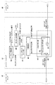
図2は、実施形態における記録装置の基板上に実装させた制御部のブロック構成図である。制御部は、複数個(図示では符号17,31,45の3つ)の同一構成のコントロールチップ(以下、単にチップ)を縦列に接続したマルチチップ構成を有する。
FIG. 2 is a block configuration diagram of a control unit mounted on the substrate of the recording apparatus according to the embodiment. The control unit has a multi-chip configuration in which a plurality of (three in the figure,
チップ17は、プログラムに従って処理を実行するCPU19、外部装置との通信を行うためのI/F処理部18、描画処理や2値化処理等を行う画像処理部21、印刷装置の記録ヘッドの駆動を制御するためのヘッド制御部22を有する。また、チップ17は、記録ヘッドや記録媒体を搬送するモーターの制御、並びに、モーターの回転速度や位置を検出するモーター・センサー制御部23、他のチップとの通信を行うためのチップ間通信部24を有する。また、チップ17は、各回路への必要な周波数のクロック信号を発生するクロック制御部25、CPU19へのリセット信号の供給を制御するリセット制御部26、ウォッチドッグタイマ部28、割り込み制御部27を有する。また、チップ17は、IO切り替え部30、及びIO切り替え部30を制御するIO制御部29を有する。
The
また、チップ17には、CPU19が実行するプログラムを格納したROM及びワークエリアとして使用するRAMで構成される外部メモリ20が接続されている。また、チップ17には、チップ31やチップ45への電力供給や、記録ヘッド1の駆動や、記録ヘッド1並びに記録媒体15の搬送を行うモーター等の、大きな電力を消費する部分への電力供給を制御するための電源制御部70が接続されている。そして、チップ17には、印刷データの発生源であるPC等のホスト16が接続されている。接続形態は、ネットワークインターフェース、USBインターフェース等があり、その種類は問わない。また、チップ17には、そのチップ17をリセットするためのリセットIC59が接続されている。
The
以上がチップ17の構成とそれに接続された構成要素の説明である。チップ31、チップ45は、チップ17と同じである。従って、図示の符号32乃至43、46乃至57は、符号18乃至30と同じであるので説明は省略する。ただし、チップ31、45には図示のごとく、用紙搬送エンコーダ11、用紙搬送モーター9、記録ヘッド1、キャリッジエンコーダ60、キャリッジモーター14が接続されている。また、外部メモリ44,58を構成するROMには、それぞれのチップに特化したプログラムが格納されることになる。
The above is the description of the configuration of the
ホスト16と接続されるチップ17のリセットは上記のようにリセットIC59からの信号によりリセットされる。そして、チップ17に接続される2番目、3番目のチップ31,45のチップリセットは、それぞれの前段(上流側)のチップにより制御される。
The
それぞれのチップは、チップ間通信部24、37、51によって接続され各チップ間で制御コマンドのやり取りや、データ転送が行われる。
Each chip is connected by
また、このチップ17は、IF処理部18を介して、ホスト16から送信された制御コマンドや記録データの受信処理を行う。そして、チップ17のCPU19は、ホスト16から受信された制御コマンドを解析し、この制御コマンドに従って記録装置の制御を行う。尚、外部メモリ20には、上記CPU19が動作するためのプログラムや記録制御回路部23の制御に必要な各種テーブルなどが格納されている。また、チップ31や、チップ45にもCPU32、46が内蔵され、それぞれのチップで必要なプログラムや各種テーブル等が外部メモリ44、58に格納されている。
Further, the
受信された記録データはチップ間通信部24、37、51を通じて、後段(下流側)のチップ31やチップ45に送られ、記録方法に応じた各種の画像処理が施された上で外部メモリ44、58に一旦格納される。外部メモリ44、58には、少なくとも1走査分の記録ヘッド1を駆動するための記録データが格納されている。さらに、マルチパス記録を行うため、又は記録データを2つのノズルに分配して記録するためなどに用いられる画像マスク等も格納されている。
The received recording data is sent to the later-stage (downstream side)
記録ヘッドに接続されているチップ31、46内のCPU32、46は、チップ17からのデータに基づき、印刷処理を実行する。具体的には、CPU32、46は、外部メモリ44,58のRAMに、印刷用の画像データの生成、格納を行う。また、用紙搬送エンコーダ11やキャリッジエンコーダ60からの信号を基にモーター・センサー制御部36、50は記録タイミング信号を生成する。この記録タイミング信号の発生をトリガに、CPU32、46は、外部メモリ44,58に格納された記録データを、ヘッド制御部35、49を介して記録ヘッド1へ送信することで印刷処理を行う。
The
[第1の実施形態]
以下、図2及び図3に従って第1の実施形態の詳細な制御方法について説明する。
[First Embodiment]
Hereinafter, a detailed control method of the first embodiment will be described with reference to FIGS. 2 and 3.
第1の実施形態では、電子機器として、3チップを縦列接続するシステム(印刷装置)を例として示す。3チップを用いたシステムを構成する事で、メモリ帯域、画像処理機能、端子機能を分散して処理させる事が可能となり、システム全体の処理能力の向上と、使用可能なIO数を増加させる事が可能となる。 In the first embodiment, a system (printing apparatus) in which three chips are connected in cascade is shown as an example of an electronic device. By configuring a system using three chips, it is possible to distribute and process memory bandwidth, image processing functions, and terminal functions, improving the overall processing capacity and increasing the number of usable IOs. Is possible.
ホスト16と接続されている1番目のチップ17は、主にI/F処理や電源制御等のシステム全体を管理するメインチップとしての役割を果たし、そのリセットについては外部ICによるリセット制御が行われる。また、2番目以降のチップ31、及び45については、主にモーターやセンサー制御、記録ヘッドの駆動制御等を行うサブチップとしての役割を果たす。また、チップ31、及び45については、自チップの前段に位置するチップの汎用のIOを用いてリセット制御信号が行われる。また、リセット制御を行う端子は汎用のIOの為、リセット状態では入力状態で、システムが起動後に出力に切り替えて使用される。この為、端子を出力に切り替えて制御できる状態にするまでの論理を固定しておく必要があり、外部抵抗を用意して固定する。また、固定する論理は、チップがリセット状態の時に、リセット信号が接続されている対向チップがリセットされる論理とする。こうする事で、例えば、2番目のチップ31がリセットされた場合、2番目のチップでリセット制御している3番目のチップ45も自動的にリセットされる構成とする事が可能となる。
The
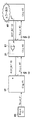
図3に、チップ31のウォッチドックタイマ部41の周囲の構成と、チップ17、45との接続例を示す。ウォッチドックタイマ部41は、ウォッチドックタイマ機能によってエラーを検知した場合、WDT_INT信号を出力する機能を有する。WDT_INT切り替え部61は、論理回路63を有する。この論理回路63は、自チップのウォッチドックタイマ部41で生成されるWDT_INT信号と、後段につながっているチップ45から出力されてコントロールチップ31へ入力されるWDT_INT外部入力信号とを論理和の演算するORゲートを有する。そして、論理回路63は、その論理和信号を、コントローラチップ17へWDT_INT外部出力信号として出力する。このように、論理回路63により、下段に位置するコントローラチップで発生したウォッチドックタイマの割り込み信号WDT_INTがファームウェアの介在なく先頭(最上流)のコントローラチップまで供給することが可能になる。つまり、WDT_INT切り替え部61は、自チップと下流側のチップそれぞれのウォッチドッグタイマからの割り込み信号を上流側のチップに伝達する伝達部として機能する。また、割り込み制御部40は、後段のコントローラチップからWDT_INT信号を受信した場合、その信号を受信したことを示すことを自チップのCPUに通知する通知部として機能する。具体的には、後段のコントローラチップからWDT_INT信号を受信した場合、割り込み制御部40は割り込み信号をCPUに供給する。
FIG. 3 shows a configuration around the
また、この対向チップへ出力されるWDT_INT信号は、IO制御部42で生成される起動完了通知信号とWDT_INT切り替え部61のセレクタ62において、切り替えてIOを共有する。各コントロールチップの電源が投入され起動が完了した場合は、この信号をCPUから制御する事によって、各コントロールチップの起動状態を示す信号として使用するが、起動完了後にはウォッチドックタイマの割り込み信号を伝達する信号に切り換える。この為、本実施形態における機能を実現する為に、新たに別の信号を用意する事無く、他のコントロールチップのエラー状態を共有する事が可能となる。
Further, the WDT_INT signal output to the opposite chip is switched and shared by the activation completion notification signal generated by the
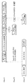
図4にウォッチドックタイマの機能によってエラーを検出し、実際にシステムリセットがされるまでのタイミングチャートを示す。実際にエラーを検出すると、ウォッチドックタイマ部41から出力されるWDT_INT信号がアサートされる。実施形態では、この段階ですぐにシステムのリセットがかかる訳ではない。つまり、WDT_INT信号がアサートされてからリセット制御部39に対して各モジュールのリセット処理を実行させる為の制御信号WD_RST_EN信号がアサートされるまで、所定の時間がかかるようにした。この時間は、外部から適宜設定できるようにしても良い。そして、この時間を利用し、エラーが発生したチップよりも前段に位置するチップ間で、エラー発生を共有する。図4では一例として、エラーが発生してWDT_INT信号がアサート後、10秒後にリセットされるタイミングチャートを記載している。この時間があれば、外部に出力されるWDT_INTを利用して対向チップとのエラー状態の共有は十分に実施する事ができる。
FIG. 4 shows a timing chart until an error is detected by the function of the watchdog timer and the system is actually reset. When an error is actually detected, the WDT_INT signal output from the
以下、具体的な構成図を示した図5と、処理の流れを示した図6に従って、3チップ目のチップ45においてエラーが発生し、ウォッチドックタイマが動作した場合の例を説明する。3チップ目のチップ45でウォッチドックタイマが動作すると、WDT_INT#3信号が、2チップ目のチップ31のWDT_INT切り替え部61にある論理回路を通過して、1番目のチップ17へ到達する。この結果、システム全体を管理している1番目のチップ17は、2番目以降のチップにエラーが発生していること認識可能となる。また、並行して3番目のチップ45は、適当な時間が経過(実施形態では10秒)してから、ウォッチドック機能によってチップ全体がリセットされる。1番目のチップ17は、後段チップからのウォッチドックの割り込み信号WDT_INT信号を受信したことに応じて、電源制御部70を制御し、大きな電力を消費するモーターや、ヘッド等への電力供給を停止させる。この電力供給の制御処理を開始するタイミングは、3番目のチップ45がリセットされるタイミングより十分に早い。つまり、3番目チップ45がリセットされる以前に、システム全体を安全な状態に移行させることが可能となる。そして、チップ17は、係る制御を行った後、後段チップへ順次アクセスを試していく事で、どのチップでエラーが発生したかを把握する事ができるようになる。また、全チップが正常になったことを受けて、チップ17は電源制御部70を制御し、電力供給を行い、再び印刷可能状態に復帰する。
Hereinafter, an example in which an error occurs in the
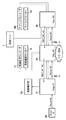
[第2の実施形態]
第2の実施形態では、最上流のチップに並列に2チップが接続され、且つ、それぞれのチップに更に縦列にチップが接続されている構成を例として示す。また、第2の実施形態では、4チップ目のチップにおいてエラーが発生し、ウォッチドックタイマが動作した場合を例として示す。記録装置の具体的な構成を図7に示す。以下、処理の流れを示した図8に従って説明する。
[Second Embodiment]
In the second embodiment, a configuration in which two chips are connected in parallel to the most upstream chip, and chips are further connected to each chip in a column is shown as an example. In the second embodiment, an example in which an error occurs in the fourth chip and the watchdog timer operates is shown as an example. A specific configuration of the recording apparatus is shown in FIG. In the following, description will be given with reference to FIG.
今、4チップ目のチップ64でウォッチドックタイマによるエラーを検知すると、WDT_INT#4信号が、チップ45、チップ31のWDT_INT切り替え部にある論理回路を通過して1番目のチップ17へ到達する。信号が到達後、システム全体を管理している1番目のチップ17は、2番目以降のチップでエラーが発生していること認識する。また、並行してチップ64はウォッチドック機能によってチップ全体がリセットされる。合わせて、チップ64によってリセットの制御を行っているチップ65もリセットされ、チップ64及びチップ65は安全な状態に変化させる事ができる。1番目のチップ17は、第1の実施形態と同様に後段チップからのウォッチドックの割り込み信号WDT_INT信号を受信したことに応じて、電源制御部70を制御し、大きな電力を消費するモーターや、ヘッド等への電力供給を停止させる。この結果、システム全体を安全な状態に移行させることができる。この後、チップ17は、後段チップへ順次アクセスを試していく事で、どのチップでエラーが発生したかを把握する事ができる。
Now, when an error due to the watchdog timer is detected in the
本第2の実施形態においては、チップ45までのアクセスは確認できるが、チップ64へのアクセスは、チップ64にリセットが入り初期状態となっている為、正しくアクセスする事が出来ず、チップ64でエラーが発生した事を確認する事ができる。
In the second embodiment, the access to the
[第3の実施形態]
第3の実施形態では、3チップが縦列に接続されているシステムにおいて、2チップ目においてウォッチドックタイマが動作した場合を例として示す。具体的な構成図は、図9に示す。本第3の実施形態では、記録動作に必要なモーター・エンコーダ―制御、及びヘッド制御をチップ31、チップ45で分散して処理させる場合を例として示している。こうする事で、システム全体の処理を分散化させる事が可能となり、より高速な記録動作が可能となる。
[Third Embodiment]
In the third embodiment, an example in which a watchdog timer operates in the second chip in a system in which three chips are connected in a column is shown as an example. A specific configuration diagram is shown in FIG. In the third embodiment, a case where motor encoder control and head control necessary for the recording operation are distributed and processed by the
通常、記録動作時は、チップ17に入力されるデータに基づいて、記録装置内のモーターやエンコーダ、ヘッド制御等を動作させ記録用紙へ記録を行う。しかしながら、記録動作の途中で、エラーが発生し、ウォッチドックタイマが動作した場合、用紙を送っている用紙搬送モーター9や、記録ヘッドの動作制御を行っているキャリッジモーター14が止まってしまうことになる。また、それぞれのモーターの位置検出に使用されるエンコーダも止まってしまう。その為、記録途中の用紙も意図しない状態で止まり、次に復帰した時に問題となる場合がある。
Normally, during a recording operation, recording is performed on recording paper by operating motors, encoders, head control, and the like in the recording apparatus based on data input to the
システム全体をコントロールしているチップ17でウォッチドックタイマが動作した場合は、システム全体に対して再起動をかける事が可能となり、メカの初期化も行われ、記録途中の用紙は正常に処理される。しかしながら、例えば、本第3の実施形態の様に2チップ目のチップ31でエラーが発生し、ウォッチドックタイマが動作した場合は、その後の再起動処理の手順を正しく行う必要がある。具体的には、途中で止まっている記録ヘッドの退避や、記録用紙を強制的に排出する処理が必要となる。
When the watchdog timer operates on the
以下、処理の流れを示した図10に従って説明する。2チップ目のチップ31でウォッチドックタイマによるエラーを検知すると、WDT_INT#2信号が、1チップ目17へ出力される。その後、システム全体を管理している1番目のチップ17は、2番目以降のチップでエラーが発生していること認識する。また、並行してチップ31は所定時間経過後にウォッチドック機能によってチップ全体がリセットされる。合わせて、チップ31によってリセットの制御を行っているチップ45もリセットされ、チップ31及びチップ45は安全な状態に変化させる事ができる。チップ17は、第1の実施形態と同様である。つまり、チップ17は、後段のチップからのウォッチドックの割り込み信号WDT_INT信号を受信後、電源制御部70を制御し、まずは大きな電力を消費するモーターや、ヘッド等への電力供給を一旦停止させ、システム全体を安全な状態に移行させる。そして、チップ17は、後段チップへ順次アクセスを試し2番目のチップ31でエラーが発生している事を把握する。
Hereinafter, description will be given with reference to FIG. When an error due to the watchdog timer is detected in the
チップ17は、2番目のチップ31でエラーを通知した後、システムとして問題が無いようであれば、チップ31の再起動処理を行う。チップ17は、チップ31との通信が出来るようになった後、続けて3番目のチップ45の再起動処理を行うが、並行して2番目のチップ31のメカの初期化処理を実施する。また、チップ45が通信可能となった後も同様に、チップ45のメカの初期化処理を実施する。この様な構成を有する事で、モーターやセンサー、記録ヘッドを制御しているチップでエラーが発生し、チップの再起動が必要な状況となった場合、少なくともエラーが発生したチップよりも前段のチップ間でエラー状態の共有することができる。故に、エラーが発生した時の記録装置の状態に応じて、記録ヘッドや記録用紙を退避させるなどして、装置の状態をより安全な状態にする事が可能となる。
The
以上述べた様に、本実施形態によれば、複数のチップを接続して構成されたシステムにおいて、いずれかのチップで発生したエラー状態をCPUの介在無しに最上流のチップまで通知する事が可能となり、エラー状態の共有が可能となる。また、エラーが発生したチップを含む下流のチップをリセットする構成を有する事で、どのチップでエラーが発生してもシステム全体を安全に停止、または再起動させる事が可能となる。また、起動完了通知信号と機能を共有する事で、前記機能を実現するために、新たな専用の端子を用意する事なく実現が可能となる。 As described above, according to the present embodiment, in a system configured by connecting a plurality of chips, an error state occurring in any one of the chips can be notified to the most upstream chip without intervention of the CPU. It becomes possible to share the error state. In addition, since the downstream chip including the chip in which the error has occurred is reset, the entire system can be safely stopped or restarted regardless of which chip has the error. In addition, by sharing the function with the activation completion notification signal, the function can be realized without preparing a new dedicated terminal.
17、31,45、64,65…コントロールチップ、16…ホスト、19,32,46…CPU、28,41、55…ウォッチドッグタイマ部、27,40,54…割り込み制御部、30,43,57…IO切り替え部、27,40、54…割り込み制御部 17, 31, 45, 64, 65 ... control chip, 16 ... host, 19, 32, 46 ... CPU, 28, 41, 55 ... watchdog timer unit, 27, 40, 54 ... interrupt control unit, 30, 43, 57: IO switching unit, 27, 40, 54 ... interrupt control unit
Claims (12)
第1のコントロールチップの下流側に第2のコントロールチップが配置され、且つ、前記第2のコントロールチップの下流側に第3のコントロールチップが配置され、
前記第2のコントロールチップは、
ウォッチドッグタイマと、
下流側に位置する前記第3のコントロールチップのウォッチドッグタイマが発生する割り込み信号と、自チップが有するウォッチドックタイマが発生する割り込み信号との論理和信号を、前記自チップが有するウォッチドッグタイマから割り込み信号として、上流側に位置する前記第1のコントロールチップに供給するための伝達部と
を有することを特徴とする電子機器。 An electronic device in which a plurality of control chips are connected in cascade,
A second control chip is disposed downstream of the first control chip, and a third control chip is disposed downstream of the second control chip;
The second control chip is
A watchdog timer,
A logical sum signal of an interrupt signal generated by the watchdog timer of the third control chip located on the downstream side and an interrupt signal generated by the watchdog timer of the own chip is transmitted from the watchdog timer of the own chip. An electronic device comprising: a transmission unit configured to supply the interrupt signal to the first control chip located on the upstream side.
Priority Applications (2)
| Application Number | Priority Date | Filing Date | Title |
|---|---|---|---|
| JP2015110801A JP6498043B2 (en) | 2015-05-29 | 2015-05-29 | Electronics |
| US15/152,983 US9652702B2 (en) | 2015-05-29 | 2016-05-12 | Electronic apparatus |
Applications Claiming Priority (1)
| Application Number | Priority Date | Filing Date | Title |
|---|---|---|---|
| JP2015110801A JP6498043B2 (en) | 2015-05-29 | 2015-05-29 | Electronics |
Publications (3)
| Publication Number | Publication Date |
|---|---|
| JP2016224730A JP2016224730A (en) | 2016-12-28 |
| JP2016224730A5 JP2016224730A5 (en) | 2018-07-05 |
| JP6498043B2 true JP6498043B2 (en) | 2019-04-10 |
Family
ID=57397225
Family Applications (1)
| Application Number | Title | Priority Date | Filing Date |
|---|---|---|---|
| JP2015110801A Active JP6498043B2 (en) | 2015-05-29 | 2015-05-29 | Electronics |
Country Status (2)
| Country | Link |
|---|---|
| US (1) | US9652702B2 (en) |
| JP (1) | JP6498043B2 (en) |
Families Citing this family (6)
| Publication number | Priority date | Publication date | Assignee | Title |
|---|---|---|---|---|
| CN106126470B (en) * | 2016-06-30 | 2021-09-17 | 唯捷创芯(天津)电子技术股份有限公司 | Variable signal flow direction control method for realizing chip reuse and communication terminal |
| CN106648950A (en) * | 2016-12-29 | 2017-05-10 | 厦门金龙联合汽车工业有限公司 | Control circuit for external watchdog when online debugging is carried out |
| JP7258467B2 (en) * | 2018-03-19 | 2023-04-17 | キヤノン株式会社 | Electronic equipment and its control method |
| US10942798B2 (en) * | 2018-05-31 | 2021-03-09 | Microsoft Technology Licensing, Llc | Watchdog timer hierarchy |
| US11144358B1 (en) * | 2018-12-06 | 2021-10-12 | Pure Storage, Inc. | Asynchronous arbitration of shared resources |
| CN110162421B (en) * | 2019-04-28 | 2020-11-10 | 北京航空航天大学 | Embedded software watchdog test method and device containing interrupt function |
Family Cites Families (10)
| Publication number | Priority date | Publication date | Assignee | Title |
|---|---|---|---|---|
| US4280060A (en) * | 1980-06-09 | 1981-07-21 | General Electric Company | Dedicated microcomputer-based control system for steam turbine-generators |
| JPH0273451A (en) * | 1988-09-08 | 1990-03-13 | Canon Inc | Controller |
| JPH02244375A (en) * | 1989-03-17 | 1990-09-28 | Fujitsu Ltd | Alarm control system |
| JPH0810439B2 (en) * | 1990-03-01 | 1996-01-31 | 株式会社ユニシアジェックス | Fail-safe device for electronic control unit |
| JP2006157387A (en) * | 2004-11-29 | 2006-06-15 | Toshiba Elevator Co Ltd | Distributed type microcomputer controller using serial communication and elevator controller |
| DE102010041003A1 (en) | 2010-09-20 | 2012-03-22 | Sb Limotive Company Ltd. | Method for monitoring at least two microcontrollers |
| JP5968119B2 (en) * | 2012-06-27 | 2016-08-10 | キヤノン株式会社 | Communication system with cascade connection |
| JP6191211B2 (en) * | 2013-04-16 | 2017-09-06 | 株式会社リコー | Electronic apparatus, image processing apparatus, and signal transmission method |
| JP6218510B2 (en) * | 2013-09-02 | 2017-10-25 | キヤノン株式会社 | Image processing apparatus, image processing apparatus control method, and program |
| JP6264896B2 (en) * | 2014-01-16 | 2018-01-24 | 株式会社リコー | Information processing apparatus, control method, and control program |
-
2015
- 2015-05-29 JP JP2015110801A patent/JP6498043B2/en active Active
-
2016
- 2016-05-12 US US15/152,983 patent/US9652702B2/en active Active
Also Published As
| Publication number | Publication date |
|---|---|
| JP2016224730A (en) | 2016-12-28 |
| US20160350634A1 (en) | 2016-12-01 |
| US9652702B2 (en) | 2017-05-16 |
Similar Documents
| Publication | Publication Date | Title |
|---|---|---|
| JP6498043B2 (en) | Electronics | |
| JP5651958B2 (en) | Printing control apparatus, printing control system, printing apparatus, and printing control method | |
| JP2012139886A (en) | Image recording apparatus and program | |
| US20110273507A1 (en) | Printhead and printing apparatus | |
| JP4612867B2 (en) | Power supply circuit, motor driver circuit, electronic device, and recording apparatus | |
| US10974500B2 (en) | Printing device and control method for printing device | |
| US10740056B2 (en) | Printing apparatus, control method of printing apparatus and storage medium | |
| JP5997461B2 (en) | Recording device | |
| JP6641735B2 (en) | Printing apparatus, printing method, and program | |
| JP7258467B2 (en) | Electronic equipment and its control method | |
| US20110058879A1 (en) | Printing device and method | |
| JP2012187918A (en) | Recording apparatus and electronic device | |
| JP6877244B2 (en) | Recording device and its control method | |
| JP2005238556A (en) | Image forming apparatus, and image formation control program | |
| JP2011177912A (en) | Printing system and control method thereof | |
| US20240004595A1 (en) | Server device, method of controlling server device, and printing system | |
| JP2002321342A (en) | Printing device | |
| US9162478B2 (en) | Image recording apparatus and nontransitory storage medium storing program | |
| US10675864B2 (en) | Printing apparatus and print control method | |
| JP5772872B2 (en) | Image recording apparatus and program | |
| WO2024062736A1 (en) | Electrical device | |
| JP2014000714A (en) | Recording head and recording device that performs recording using the recording head | |
| JP3884924B2 (en) | Printhead heater board | |
| JP2009269356A (en) | Image forming apparatus and scanning control method | |
| JP2018192791A (en) | Element substrate, recording head, and recording apparatus |
Legal Events
| Date | Code | Title | Description |
|---|---|---|---|
| A521 | Request for written amendment filed |
Free format text: JAPANESE INTERMEDIATE CODE: A523 Effective date: 20180525 |
|
| A621 | Written request for application examination |
Free format text: JAPANESE INTERMEDIATE CODE: A621 Effective date: 20180525 |
|
| A977 | Report on retrieval |
Free format text: JAPANESE INTERMEDIATE CODE: A971007 Effective date: 20190123 |
|
| TRDD | Decision of grant or rejection written | ||
| A01 | Written decision to grant a patent or to grant a registration (utility model) |
Free format text: JAPANESE INTERMEDIATE CODE: A01 Effective date: 20190212 |
|
| A61 | First payment of annual fees (during grant procedure) |
Free format text: JAPANESE INTERMEDIATE CODE: A61 Effective date: 20190312 |
|
| R151 | Written notification of patent or utility model registration |
Ref document number: 6498043 Country of ref document: JP Free format text: JAPANESE INTERMEDIATE CODE: R151 |