JP6483963B2 - Power converter - Google Patents
Power converter Download PDFInfo
- Publication number
- JP6483963B2 JP6483963B2 JP2014120118A JP2014120118A JP6483963B2 JP 6483963 B2 JP6483963 B2 JP 6483963B2 JP 2014120118 A JP2014120118 A JP 2014120118A JP 2014120118 A JP2014120118 A JP 2014120118A JP 6483963 B2 JP6483963 B2 JP 6483963B2
- Authority
- JP
- Japan
- Prior art keywords
- gate
- emitter terminal
- terminal
- emitter
- main
- Prior art date
- Legal status (The legal status is an assumption and is not a legal conclusion. Google has not performed a legal analysis and makes no representation as to the accuracy of the status listed.)
- Active
Links
Images


Classifications
-
- H—ELECTRICITY
- H02—GENERATION; CONVERSION OR DISTRIBUTION OF ELECTRIC POWER
- H02M—APPARATUS FOR CONVERSION BETWEEN AC AND AC, BETWEEN AC AND DC, OR BETWEEN DC AND DC, AND FOR USE WITH MAINS OR SIMILAR POWER SUPPLY SYSTEMS; CONVERSION OF DC OR AC INPUT POWER INTO SURGE OUTPUT POWER; CONTROL OR REGULATION THEREOF
- H02M7/00—Conversion of ac power input into dc power output; Conversion of dc power input into ac power output
- H02M7/003—Constructional details, e.g. physical layout, assembly, wiring or busbar connections
-
- H—ELECTRICITY
- H01—ELECTRIC ELEMENTS
- H01L—SEMICONDUCTOR DEVICES NOT COVERED BY CLASS H10
- H01L25/00—Assemblies consisting of a plurality of individual semiconductor or other solid state devices ; Multistep manufacturing processes thereof
- H01L25/03—Assemblies consisting of a plurality of individual semiconductor or other solid state devices ; Multistep manufacturing processes thereof all the devices being of a type provided for in the same subgroup of groups H01L27/00 - H01L33/00, or in a single subclass of H10K, H10N, e.g. assemblies of rectifier diodes
- H01L25/10—Assemblies consisting of a plurality of individual semiconductor or other solid state devices ; Multistep manufacturing processes thereof all the devices being of a type provided for in the same subgroup of groups H01L27/00 - H01L33/00, or in a single subclass of H10K, H10N, e.g. assemblies of rectifier diodes the devices having separate containers
-
- H—ELECTRICITY
- H01—ELECTRIC ELEMENTS
- H01L—SEMICONDUCTOR DEVICES NOT COVERED BY CLASS H10
- H01L2924/00—Indexing scheme for arrangements or methods for connecting or disconnecting semiconductor or solid-state bodies as covered by H01L24/00
- H01L2924/0001—Technical content checked by a classifier
- H01L2924/0002—Not covered by any one of groups H01L24/00, H01L24/00 and H01L2224/00
Description
本発明は、電力変換装置に関し、特に鉄道車両に用いられる電力変換装置に適用して好適なものである。 The present invention relates to a power conversion device, and is particularly suitable for application to a power conversion device used in a railway vehicle.
一般に鉄道車両に用いられる電力変換装置は、直流電力を交流電力に変換するインバータ、交流電力を直流電力に変換するコンバータ及び直流電圧を昇圧又は降圧する直流チョッパ等の回路を備えて構成される。またこれらの回路においては、IGBT(Insulated Gate Bipolar Transistor)と呼ばれるパワー半導体が広く用いられている。 2. Description of the Related Art Generally, a power conversion device used for a railway vehicle includes a circuit such as an inverter that converts DC power into AC power, a converter that converts AC power into DC power, and a DC chopper that boosts or steps down a DC voltage. In these circuits, a power semiconductor called IGBT (Insulated Gate Bipolar Transistor) is widely used.
パワー半導体は、ゲート駆動基板からのオン及びオフの信号により駆動し、ゲート駆動基板は、変換器のコントローラである制御理論部からの信号により駆動する。パワー半導体とゲート駆動基板とはゲート配線と呼ばれる配線により接続されており、このゲート配線で両者を接続することで、ゲート駆動基板はパワー半導体を流れる電流を検出することができる。 The power semiconductor is driven by on and off signals from a gate drive substrate, and the gate drive substrate is driven by a signal from a control theory unit which is a controller of the converter. The power semiconductor and the gate drive substrate are connected to each other by a wiring called a gate wiring, and the gate drive substrate can detect a current flowing through the power semiconductor by connecting both of them with the gate wiring.
ゲート駆動基板にはパワー半導体を保護するための保護機能が搭載されており、保護機能の一つに短絡保護機能がある。短絡の判断に際してはパワー半導体を含むモジュール(パワー半導体モジュールと呼ぶ)の内部に設置された主エミッタ端子と補助エミッタ端子との間のエミッタインダクタンス間に発生する電圧に基づいて短絡を判断する方法がある。 The gate drive substrate is equipped with a protection function for protecting the power semiconductor, and one of the protection functions is a short-circuit protection function. When determining a short circuit, there is a method for determining a short circuit based on a voltage generated between an emitter inductance between a main emitter terminal and an auxiliary emitter terminal installed in a module including a power semiconductor (referred to as a power semiconductor module). is there.
特許文献1には、エミッタインダクタンス間に発生する電圧に基づいて短絡を判断する短絡保護機能を搭載した電力変換装置が開示されている。具体的にはスイッチング素子(パワー半導体)の主端子と直列にインダクタンスを設置し、スイッチング時にインダクタンスの両端に発生する電圧を積分回路で積分することにより、パワー半導体に流れる電流を検出して短絡を判断する技術が開示されている。
しかし特許文献1に記載の電力変換装置においては、パワー半導体モジュールとゲート駆動基板とを接続するゲート配線の具体的な構成について何ら開示されていない。
However, the power conversion device described in
図7は、一般的なゲート配線の構成を示す。ゲート配線は、主エミッタ端子とゲート駆動基板との間を接続する主エミッタ配線と、補助エミッタ端子とゲート駆動基板との間を接続する補助エミッタ配線とから構成される。 FIG. 7 shows a configuration of a general gate wiring. The gate wiring is composed of a main emitter wiring that connects the main emitter terminal and the gate drive substrate, and an auxiliary emitter wiring that connects the auxiliary emitter terminal and the gate drive substrate.
またゲート配線は、インダクタンスをできるだけ小さくするため、一般に主エミッタ配線及び補助エミッタ配線の2本の配線をより線にして形成される。しかしこの場合、インダクタンスを一定値よりも更に小さくすることができず、また配線に重畳したコモンモードノイズによりパワー半導体に流れる電流を誤検出する場合がある。 Further, the gate wiring is generally formed by making two wirings of the main emitter wiring and the auxiliary emitter wiring stranded to make the inductance as small as possible. However, in this case, the inductance cannot be made smaller than a certain value, and the current flowing through the power semiconductor may be erroneously detected due to common mode noise superimposed on the wiring.
本発明は以上の点を考慮してなされたもので、ゲート配線のインダクタンスを最小化して電流検出精度を向上し得る電力変換装置を提案する。 The present invention has been made in consideration of the above points, and proposes a power conversion device that can improve the current detection accuracy by minimizing the inductance of the gate wiring.
本発明の電力変換装置においては、主エミッタ端子、ゲート端子及び補助エミッタ端子を備えるパワー半導体モジュールと、前記パワー半導体モジュールに接続されるゲート駆動基板とを備える鉄道車両用の電力変換装置において、前記パワー半導体モジュールと前記ゲート駆動基板とを金属導体板により接続し、前記パワー半導体モジュールは、2つの凸部及び平坦部を備え、前記2つの凸部のそれぞれに前記主エミッタ端子を備え、前記平坦部に2組の前記ゲート端子及び前記補助エミッタ端子を備え、前記ゲート駆動基板は、前記平坦部の上面に設置されることにより前記平坦部に設置された前記2組のゲート端子及び補助エミッタ端子とそれぞれ接続し、前記金属導体板は、前記2つの凸部に跨って前記2つの凸部の上面に設置される第1の金属導体板と、前記2つの凸部のうちの何れか一方の凸部の上面に設置される第2の金属導体板とから構成され、前記第1の金属導体板は、一部が前記2つの凸部のうちの何れか一方の凸部に設置された前記主エミッタ端子と接続し、他部が他方の凸部の側面に沿って直下するように設置されることにより前記一方の凸部に設置された前記主エミッタ端子と、前記平坦部に設置された前記ゲート駆動基板とを接続し、前記第2の金属導体板は、一部が前記他方の凸部に設置された前記主エミッタ端子と接続し、他部が前記他方の凸部の側面に沿って直下するように設置されることにより前記他方の凸部に設置された前記主エミッタ端子と、前記平坦部に設置された前記ゲート駆動基板とを接続することを特徴とすることを特徴とする。 In the power conversion device of the present invention, in a power conversion device for a railway vehicle comprising a power semiconductor module comprising a main emitter terminal, a gate terminal and an auxiliary emitter terminal, and a gate drive substrate connected to the power semiconductor module, A power semiconductor module and the gate drive substrate are connected by a metal conductor plate, the power semiconductor module includes two convex portions and a flat portion, each of the two convex portions includes the main emitter terminal, and the flat Two sets of the gate terminal and the auxiliary emitter terminal are provided in the part, and the gate driving substrate is installed on the upper surface of the flat part, so that the two sets of gate terminal and auxiliary emitter terminal installed on the flat part And the metal conductor plate is installed on the upper surface of the two convex portions across the two convex portions. The first metal conductor plate is composed of a first metal conductor plate and a second metal conductor plate installed on the upper surface of any one of the two protrusions. Is connected to the main emitter terminal disposed on one of the two convex portions, and the other portion is disposed so as to be directly below the side surface of the other convex portion. The main emitter terminal installed on the convex part of the gate is connected to the gate driving substrate installed on the flat part, and the second metal conductor plate is partly installed on the other convex part The main emitter terminal connected to the main emitter terminal and installed on the flat portion by installing the main emitter terminal on the other convex portion by installing the other portion directly below the side surface of the other convex portion. characterized in that characterized in that it connects the gate drive substrate that is
本発明によれば、ゲート配線のインダクタンスを最小化して電流検出精度を向上することができる。 According to the present invention, the current detection accuracy can be improved by minimizing the inductance of the gate wiring.
以下図面について、本発明の一実施の形態を詳述する。 Hereinafter, an embodiment of the present invention will be described in detail with reference to the drawings.
(1)全体構成
図1は、第1の実施の形態における電力変換装置の斜視構成を示す。特にここでは1つのパワー半導体モジュールに1つのパワー半導体を搭載する1in1タイプのパワー半導体モジュールを2つ備えた2レベルインバータの1相分を示す。
(1) Overall Configuration FIG. 1 shows a perspective configuration of the power conversion device according to the first embodiment. In particular, here, one phase of a two-level inverter provided with two 1 in 1 type power semiconductor modules in which one power semiconductor is mounted on one power semiconductor module is shown.
電力変換装置は、上アームの半導体モジュール(IGBTモジュール)1及び下アームのIGBTモジュール2を備える。上アームのIGBTモジュール1は下アームのIGBTモジュール2と同一の構成であるため、以下では特に下アームのIGBTモジュール2の構成について説明する。
The power converter includes an upper arm semiconductor module (IGBT module) 1 and a lower
IGBTモジュール2は、複数の主コレクタ端子21、複数の主エミッタ端子22、ゲート端子23及び補助エミッタ端子24を備えて構成される。IGBTモジュール2は、2つの凸部を有して構成され、この2つの凸部のうちの一方の凸部の上面に主コレクタ端子21が設置される。また他方の凸部の上面に主エミッタ端子22が設置される。
The
またIGBTモジュール2の上面のうち、凸部以外の平坦部にはゲート端子23及び補助エミッタ端子24が設置される。そしてこれらの端子21〜24のうち、主エミッタ端子22、ゲート端子23及び補助エミッタ端子24は、IGBTモジュール2を駆動するゲート駆動基板25に接続される。
A
ゲート駆動基板25は、ゲート端子23及び補助エミッタ端子24とは直接接続され、また複数の主エミッタ端子22とは金属導体板(エミッタセンス配線板)26を介して接続される。すなわちエミッタセンス配線板26は、複数の主エミッタ端子22とゲート駆動基板25とを接続する。
The
エミッタセンス配線板26は、IGBTモジュール2の上面のうち、主エミッタ端子22が設置されている凸部の上面を覆うように設置され、またこの凸部の側面に沿って平坦部まで直下してゲート駆動基板25に接続されるように設置される。
The emitter
またエミッタセンス配線板26は、幅W1及びW2が広いほど、主エミッタ端子22とゲート駆動基板25との間のインダクタンスを小さくすることができる。よってここでは、エミッタセンス配線板26は、主エミッタ端子22との接続部分において複数の主エミッタ端子22の設置幅以上の幅W1を有し、凸部の側面に沿って平坦部まで直下する部分においてはゲート駆動基板25との接続幅以上の幅W2を有する。
In addition, the emitter
なお電力変換装置は、上記説明してきた各部(21〜26)を備える他、正側電源(図示省略)と主コレクタ端子11とを接続する正側導体板31、上アームの主エミッタ端子12と下アームの主コレクタ端子21とを接続する中間導体板32及び負側電源(図示省略)と主エミッタ端子22とを接続する負側導体板33を備える。また交流出力端子41やIGBTモジュール2を冷却する冷却装置51等を備える。
The power converter includes the above-described units (21 to 26), a
上記説明してきた各部(21〜26)は下アームのIGBTモジュール2に関する部分であり、上アームのIGBTモジュール1についても同様に構成される。例えば下アームのエミッタセンス配線板26により主エミッタ端子22とゲート駆動基板25とが接続される構成は、上アームにおいても同様である。上アームにおいてはエミッタセンス配線板16により主エミッタ端子12とゲート駆動基板15とが接続される。
Each part (21-26) demonstrated above is a part regarding the
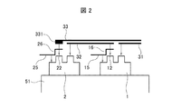
(2)側面構成
図2は、図1の電力変換装置の側面構成を示す。電力変換装置は、上記説明してきた通り、冷却装置51上に上アーム及び下アームの2つのIGBTモジュール1及び2を備える。そしてこれらIGBTモジュール1及び2がそれぞれ備える2つの凸部のうち、一方の凸部に設置される主エミッタ端子12及び22がそれぞれエミッタセンス配線板16及び26に接続される。またこれらエミッタセンス配線板16及び26は、それぞれゲート駆動基板15及び25に接続される。
(2) Side Configuration FIG. 2 shows a side configuration of the power converter of FIG. As described above, the power conversion device includes two
なお負側導体板33の端部のうち、IGBTモジュール2の凸部の上部に設置される端部の下面には高さ調節部331が設けられる。この高さ調節部331は、負側導体板33と同一の部材により構成され、負側導体板33を水平に維持する。
Of the end portions of the
(3)正面構成
図3は、図1の電力変換装置の正面構成を示す。ここでは特に下アームのIGBTモジュール2の正面構成を示す。このIGBTモジュール2を正面から見ると、主エミッタ端子22とIGBTモジュール2のパッケージ外面との間には、空隙が設けられている。なお図1及び図2においては簡素化のため空隙の図示を省略している。エミッタセンス配線板26は、平板形状であるため、この空隙に差し込んで設置することができる。
(3) Front Configuration FIG. 3 shows a front configuration of the power conversion device of FIG. Here, the front configuration of the
(4)回路構成
図4は、電力変換装置の回路構成を示す。なおここではIGBTモジュール2及び周辺の回路構成について説明するが、IGBTモジュール1及び周辺の回路構成についても同様である。電力変換装置は、上記説明してきたゲート駆動基板25及びIGBTモジュール2を備える他、制御理論部61を備えて構成される。
(4) Circuit Configuration FIG. 4 shows a circuit configuration of the power converter. Although the
制御理論部61は、オン/オフ信号S1をゲート駆動基板25に出力する。ゲート駆動基板25内部のゲート駆動回路251は、制御理論部61からのオン/オフ信号S1を入力すると、オン/オフ信号S1をIGBTモジュール2用のオン/オフ信号S2に変換し、このオン/オフ信号S2をIGBTモジュール2に出力する。
The
IGBTモジュール2内部のゲート端子23にゲート駆動回路251からのオン/オフ信号S2が入力された場合、IGBTモジュール2は、オン時においては主コレクタ端子21と主エミッタ端子22との間にコレクタ電流を流す。オフ時においては主コレクタ端子21と主エミッタ端子との間には図示しない電源電圧が印加される。
When the on / off signal S2 from the
IGBTモジュール2内部の補助エミッタ端子24は、ゲート端子23にオン/オフ信号S2が入力される際に流れる電流を流す端子であり、主エミッタ端子22とは同電位であるが、IGBTモジュール2においては主エミッタ端子22とは別端子で構成される。
The
IGBTモジュール2内部において、主エミッタ端子22と補助エミッタ端子24との間はエミッタセンス配線板26により接続されるため、寄生の配線インダクタンスLeが形成される。また主エミッタ端子22と補助エミッタ端子24とは、ゲート駆動基板25内部の電流検出回路252に接続される。
In the
電流検出回路252は、配線インダクタンスLeに発生する電圧を積分して主コレクタ端子21と主エミッタ端子22との間に流れた電流を検出し、検出結果として得られた電流情報S3を短絡判定回路253に出力する。
The
短絡判定回路253は、電流情報S3に基づいて、正常又は異常(短絡)を判定し、IGBTモジュール2が破壊されるような大電流が流れている場合には異常と判定する。この場合、短絡判定回路253は、IGBTモジュール2に流れる電流を強制的にオフにするオフ信号S4をゲート駆動回路251に出力する。この結果、IGBTの短絡保護が実現される。
The short
ここでエミッタセンス配線板26は、幅広の平板形状であり、最短経路でIGBTモジュール2とゲート駆動基板25とを接続する。エミッタセンス配線板26が幅広かつ最短経路で形成されることにより、寄生インダクタンスを最小化してノイズが重畳することを防止することができる。
Here, the emitter
よって電流検出値を誤検出したことにより短絡と判定してインバータの動作を停止すること、或いは、短絡であるにもかかわらず短絡と判定せずにインバータの動作を継続すること等の不具合を防止することができる。 Therefore, it is possible to prevent problems such as stopping the operation of the inverter due to a short circuit due to erroneous detection of the current detection value, or continuing the operation of the inverter without determining the short circuit despite the short circuit. can do.
(5)第1の実施の形態による効果
以上のように第1の実施の形態による電力変換装置によれば、IGBTモジュール1及び2に設置されている複数の主エミッタ端子12及び22と、ゲート駆動基板15及び25とをそれぞれエミッタセンス配線板16及び26により接続して両者間のインダクタンスを最小化するようにしたので、誤検出を防止して電流検出精度を向上することができる。
(5) Effects of the First Embodiment As described above, according to the power conversion device of the first embodiment, the plurality of
またエミッタセンス配線板16及び26は、互いに絶縁関係を維持することができる範囲内で幅広であり、かつ、最短経路にて主エミッタ端子12及び22と、ゲート駆動基板15及び25とをそれぞれ接続するようにしたので、インダクタンスを最小化することができる。よって誤検出を防止して電流検出精度を向上することができる。
The emitter
なお第1の実施の形態においては、ゲート駆動基板25は1枚の基板として説明したが、必ずしもこれに限らず、例えば短絡保護機能を搭載した基板と、制御理論部61からの信号を受信する基板とを別々の基板とした構成であってもよい。この場合、短絡保護機能を搭載した基板だけをIGBTモジュール1及び2の直近に配置して、この基板と主エミッタ端子12及び22との間をそれぞれ幅広のエミッタセンス配線板16及び26で最短経路により接続することで、電流検出精度を向上することができるという上記の効果を得ることができる。
In the first embodiment, the
また第1の実施の形態においては、2つのIGBTモジュール1及び2は並列接続していない構成について説明したが、必ずしもこれに限らず、例えば複数のIGBTモジュールを並列接続し、これらを一体として1枚のゲート駆動基板が接続するように構成してもよい。この場合であっても、板形状のエミッタセンス配線板を用いることにより、電流検出精度を向上することができるという上記の効果を得ることができる。
In the first embodiment, the configuration in which the two
また第1の実施の形態においては、2レベルインバータを例に説明したが、3レベル以上のマルチレベルインバータにおいても適用することができる。 In the first embodiment, the two-level inverter has been described as an example, but the present invention can also be applied to a multi-level inverter having three or more levels.
(6)第2の実施の形態
図5は、第2の実施の形態における電力変換装置の斜視構成を示す。第2の実施の形態の電力変換装置は、1つのパワー半導体モジュールに上下アームの2つのパワー半導体を搭載する2in1タイプのパワー半導体モジュールを備える点及び上下アームの2つのパワー半導体を1枚の基板で駆動する2in1タイプのゲート駆動基板を備える点て、第1の実施の形態と異なる。以下異なる構成について説明する。
(6) Second Embodiment FIG. 5 shows a perspective configuration of a power converter according to a second embodiment. The power conversion device according to the second embodiment includes a 2-in-1 type power semiconductor module in which two power semiconductors of the upper and lower arms are mounted on one power semiconductor module, and the two power semiconductors of the upper and lower arms on one substrate. The second embodiment is different from the first embodiment in that a 2-in-1 type gate drive substrate is provided. Different configurations will be described below.
IGBTモジュール2Aは、上アーム用の主コレクタ端子11A、主エミッタ端子12A、ゲート端子13A及び補助エミッタ端子14Aを備え、下アーム用の主コレクタ端子21A、主エミッタ端子22A、ゲート端子23A及び補助エミッタ端子24Aを備えて構成される。 The IGBT module 2A includes a main collector terminal 11A for the upper arm, a main emitter terminal 12A, a gate terminal 13A, and an auxiliary emitter terminal 14A, and a main collector terminal 21A, a main emitter terminal 22A, a gate terminal 23A, and an auxiliary emitter for the lower arm. A terminal 24A is provided.
これらの端子11A〜14A及び21A〜24Aのうち、主エミッタ端子12A、22A、ゲート端子13A、23A、補助エミッタ端子14A及び24Aは、それぞれIGBTモジュール2Aを駆動するゲート駆動基板25Aに接続される。 Of these terminals 11A to 14A and 21A to 24A, the main emitter terminals 12A and 22A, the gate terminals 13A and 23A, and the auxiliary emitter terminals 14A and 24A are each connected to a gate drive substrate 25A that drives the IGBT module 2A.
ゲート駆動基板25Aは、上アーム駆動用及び下アーム駆動用を一体とした1枚の基板で構成され、ゲート端子13A、23A、補助エミッタ端子14A及び24Aとは直接接続される。また主エミッタ端子12A及び22Aとはエミッタセンス配線板16A及び26Aを介して接続される。すなわちエミッタセンス配線板16A及び26Aは、主エミッタ端子12A及び22Aとゲート駆動基板25Aとを接続する。 The gate drive substrate 25A is composed of a single substrate for driving the upper arm and the lower arm, and is directly connected to the gate terminals 13A and 23A and the auxiliary emitter terminals 14A and 24A. The main emitter terminals 12A and 22A are connected via emitter sense wiring boards 16A and 26A. That is, the emitter sense wiring boards 16A and 26A connect the main emitter terminals 12A and 22A and the gate drive substrate 25A.
エミッタセンス配線板16Aは、上アームの主エミッタ端子12Aが設置されている凸部の上面を覆うように設置され、またこの凸部の側面に沿って平坦部まで直下してゲート駆動基板25Aに接続されるように設置される。 The emitter sense wiring board 16A is installed so as to cover the upper surface of the convex portion on which the main emitter terminal 12A of the upper arm is installed, and directly below the flat portion along the side surface of the convex portion to the gate drive substrate 25A. Installed to be connected.
またエミッタセンス配線板26Aは、下アームの主エミッタ端子22Aが設置されている凸部の上面を覆うように設置され、またこの凸部とは異なる他の凸部まで延在し、この他の凸部の側面に沿って平坦部まで直下してゲート駆動基板25Aに接続されるように設置される。 The emitter sense wiring board 26A is installed so as to cover the upper surface of the convex part where the main emitter terminal 22A of the lower arm is installed, and extends to another convex part different from the convex part. It is installed so as to be directly connected to the gate drive substrate 25A along the side surface of the convex portion and directly below the flat portion.
エミッタセンス配線板16A及び26Aは、幅W3及びW4が広いほど、主エミッタ端子12A及び22Aとゲート駆動基板25Aとの間のインダクタンスを小さくすることができる。よってここでは、エミッタセンス配線板16A及び26Aは、互いに絶縁関係を維持可能な範囲において最大となる幅W3及びW4を有する。 As the widths W3 and W4 of the emitter sense wiring boards 16A and 26A are wider, the inductance between the main emitter terminals 12A and 22A and the gate drive substrate 25A can be reduced. Therefore, here, the emitter sense wiring boards 16A and 26A have the maximum widths W3 and W4 in a range in which the insulation relationship can be maintained.
(7)第2の実施の形態による効果
以上のように第2の実施の形態による電力変換装置によれば、2in1タイプのIGBTモジュール2A及びゲート駆動基板25Aを備える場合であっても、主エミッタ端子12A及び22Aと、ゲート駆動基板25Aとをエミッタセンス配線板16A及び26Aにより接続して両者間のインダクタンスを最小化することができる。よって誤検出を防止して電流検出精度を向上させることができる。
(7) Effects of the Second Embodiment As described above, according to the power conversion device of the second embodiment, the main emitter is provided even when the 2-in-1 type IGBT module 2A and the gate drive substrate 25A are provided. The terminals 12A and 22A and the gate drive substrate 25A can be connected by the emitter sense wiring boards 16A and 26A to minimize the inductance between them. Therefore, erroneous detection can be prevented and current detection accuracy can be improved.
なおここでは2in1タイプのIGBTモジュール2Aを備えるとしたが、これに限らず、例えば6アーム分を1つのパッケージで構成した6in1タイプのIGBTモジュールを備えるとしてもよい。この場合であっても各主エミッタ端子とゲート駆動基板とをエミッタ配線板により接続することで、両者間のインダクタンスを最小化することができる。よって誤検出を防止して電流検出精度を向上させることができる。 Although the 2in1 type IGBT module 2A is provided here, the present invention is not limited to this. For example, a 6in1 type IGBT module in which six arms are configured in one package may be provided. Even in this case, the inductance between the main emitter terminals and the gate drive substrate can be minimized by connecting them with the emitter wiring board. Therefore, erroneous detection can be prevented and current detection accuracy can be improved.
(8)他の実施の形態
図6は、他の実施の形態における電力変換装置の斜視構成を示す。この他の電力変換装置は、エミッタセンス配線板26BがU字形状を有する点で、第1の実施の形態と異なる。エミッタセンス配線板26BがU字形状を有することにより、主エミッタ端子22がパワー半導体モジュール2に設置された後であっても、主エミッタ端子22とパワー半導体モジュール2のパッケージ外面との間の空隙にエミッタセンス配線板26Bを容易に設置することができる。
(8) Other Embodiments FIG. 6 shows a perspective configuration of a power converter according to another embodiment. This other power converter differs from the first embodiment in that the emitter sense wiring board 26B has a U shape. Since the emitter sense wiring board 26B has a U shape, the gap between the
1、2 パワー半導体モジュール(IGBTモジュール)
11、21 主コレクタ端子
12、22 主エミッタ端子
13、23 ゲート端子
14、24 補助エミッタ端子
15、25 ゲート駆動基板
16、26 金属導体板(エミッタセンス配線板)
1, 2 Power semiconductor module (IGBT module)
11, 21
Claims (2)
前記パワー半導体モジュールと前記ゲート駆動基板とを金属導体板により接続し、
前記パワー半導体モジュールは、2つの凸部及び平坦部を備え、前記2つの凸部のそれぞれに前記主エミッタ端子を備え、前記平坦部に2組の前記ゲート端子及び前記補助エミッタ端子を備え、
前記ゲート駆動基板は、前記平坦部の上面に設置されることにより前記平坦部に設置された前記2組のゲート端子及び補助エミッタ端子とそれぞれ接続し、
前記金属導体板は、前記2つの凸部に跨って前記2つの凸部の上面に設置される第1の金属導体板と、前記2つの凸部のうちの何れか一方の凸部の上面に設置される第2の金属導体板とから構成され、
前記第1の金属導体板は、一部が前記2つの凸部のうちの何れか一方の凸部に設置された前記主エミッタ端子と接続し、他部が他方の凸部の側面に沿って直下するように設置されることにより前記一方の凸部に設置された前記主エミッタ端子と、前記平坦部に設置された前記ゲート駆動基板とを接続し、
前記第2の金属導体板は、一部が前記他方の凸部に設置された前記主エミッタ端子と接続し、他部が前記他方の凸部の側面に沿って直下するように設置されることにより前記他方の凸部に設置された前記主エミッタ端子と、前記平坦部に設置された前記ゲート駆動基板とを接続することを特徴とする電力変換装置。 In a power converter for a railway vehicle comprising a power semiconductor module comprising a main emitter terminal, a gate terminal and an auxiliary emitter terminal, and a gate drive substrate connected to the power semiconductor module,
The power semiconductor module and the gate drive substrate are connected by a metal conductor plate,
The power semiconductor module includes two convex portions and a flat portion, each of the two convex portions includes the main emitter terminal, and the flat portion includes two sets of the gate terminal and the auxiliary emitter terminal,
The gate driving substrate is connected to the two sets of gate terminals and auxiliary emitter terminals installed on the flat part by being installed on the upper surface of the flat part,
The metal conductor plate is disposed on the upper surface of one of the two convex portions and the first metal conductive plate installed on the upper surface of the two convex portions across the two convex portions. A second metal conductor plate to be installed;
A part of the first metal conductor plate is connected to the main emitter terminal installed on one of the two convex parts, and the other part is along the side surface of the other convex part. Connecting the main emitter terminal installed on the one convex part by being installed directly below, and the gate driving substrate installed on the flat part,
The second metal conductor plate is installed such that a part thereof is connected to the main emitter terminal installed on the other convex part, and the other part is directly below the side surface of the other convex part. To connect the main emitter terminal installed on the other convex portion to the gate drive substrate installed on the flat portion.
Priority Applications (3)
| Application Number | Priority Date | Filing Date | Title |
|---|---|---|---|
| JP2014120118A JP6483963B2 (en) | 2014-06-11 | 2014-06-11 | Power converter |
| GB1508151.6A GB2529018B (en) | 2014-06-11 | 2015-05-13 | Power converter |
| DE102015210563.6A DE102015210563B4 (en) | 2014-06-11 | 2015-06-09 | POWER CONVERTER |
Applications Claiming Priority (1)
| Application Number | Priority Date | Filing Date | Title |
|---|---|---|---|
| JP2014120118A JP6483963B2 (en) | 2014-06-11 | 2014-06-11 | Power converter |
Publications (3)
| Publication Number | Publication Date |
|---|---|
| JP2015233395A JP2015233395A (en) | 2015-12-24 |
| JP2015233395A5 JP2015233395A5 (en) | 2016-09-29 |
| JP6483963B2 true JP6483963B2 (en) | 2019-03-13 |
Family
ID=53489541
Family Applications (1)
| Application Number | Title | Priority Date | Filing Date |
|---|---|---|---|
| JP2014120118A Active JP6483963B2 (en) | 2014-06-11 | 2014-06-11 | Power converter |
Country Status (3)
| Country | Link |
|---|---|
| JP (1) | JP6483963B2 (en) |
| DE (1) | DE102015210563B4 (en) |
| GB (1) | GB2529018B (en) |
Families Citing this family (2)
| Publication number | Priority date | Publication date | Assignee | Title |
|---|---|---|---|---|
| EP3244715A1 (en) * | 2016-05-10 | 2017-11-15 | Siemens Aktiengesellschaft | Phase module for a power converter |
| JP6828425B2 (en) * | 2016-12-26 | 2021-02-10 | 東芝三菱電機産業システム株式会社 | Power converter |
Family Cites Families (8)
| Publication number | Priority date | Publication date | Assignee | Title |
|---|---|---|---|---|
| US5422440A (en) * | 1993-06-08 | 1995-06-06 | Rem Technologies, Inc. | Low inductance bus bar arrangement for high power inverters |
| JP3454186B2 (en) | 1999-05-14 | 2003-10-06 | 株式会社日立製作所 | Power converter |
| JP2002142444A (en) * | 2000-11-07 | 2002-05-17 | Toshiba Corp | Power-converting device |
| JP3705755B2 (en) * | 2001-07-26 | 2005-10-12 | 株式会社日立製作所 | Power semiconductor device |
| JP2007185026A (en) * | 2006-01-05 | 2007-07-19 | Hitachi Ltd | Power conversion device |
| ATE528856T1 (en) * | 2009-06-19 | 2011-10-15 | Vincotech Holdings S A R L | POWER MODULE WITH ADDITIONAL TRANSIENT CURRENT PATH AND POWER MODULE SYSTEM |
| US8686288B2 (en) * | 2011-05-31 | 2014-04-01 | Tesla Motors, Inc. | Power electronics interconnection for electric motor drives |
| JP5705099B2 (en) | 2011-12-16 | 2015-04-22 | 三菱電機株式会社 | Semiconductor switching device |
-
2014
- 2014-06-11 JP JP2014120118A patent/JP6483963B2/en active Active
-
2015
- 2015-05-13 GB GB1508151.6A patent/GB2529018B/en active Active
- 2015-06-09 DE DE102015210563.6A patent/DE102015210563B4/en active Active
Also Published As
| Publication number | Publication date |
|---|---|
| JP2015233395A (en) | 2015-12-24 |
| DE102015210563A1 (en) | 2015-12-17 |
| GB2529018B (en) | 2016-08-17 |
| GB201508151D0 (en) | 2015-06-24 |
| GB2529018A (en) | 2016-02-10 |
| DE102015210563B4 (en) | 2023-01-26 |
Similar Documents
| Publication | Publication Date | Title |
|---|---|---|
| US10153708B2 (en) | Three-level power converter | |
| JP5569555B2 (en) | Wiring member and semiconductor module using the same | |
| JP6400201B2 (en) | Power semiconductor module | |
| US9214406B2 (en) | Electronic control device | |
| JP5586671B2 (en) | Power module and driving device using the same | |
| US8916967B1 (en) | Semiconductor device | |
| US20150245490A1 (en) | Electronic circuit apparatus | |
| JP6745991B2 (en) | Semiconductor power module | |
| US20150035136A1 (en) | Semiconductor device to be attached to heat radiation member | |
| JP2006197735A (en) | Inverter | |
| JP6261476B2 (en) | Power converter and output voltage detection method of power converter | |
| JP6820825B2 (en) | Semiconductor devices and their driving methods | |
| JP6483963B2 (en) | Power converter | |
| US10164530B2 (en) | Boost chopper circuit including switching device circuit and backflow prevention diode circuit | |
| JP2016115834A (en) | Electronic circuit device | |
| JP2007259690A (en) | Power module | |
| US10381947B2 (en) | Power conversion apparatus | |
| JP2015122876A (en) | Semiconductor device | |
| JP2008022648A (en) | Failure detection apparatus of power module | |
| JP6901639B1 (en) | Power conversion unit | |
| JP2019022253A (en) | Semiconductor driving device, and three-phase ac inverter mounted with the same | |
| JP4246040B2 (en) | Semiconductor device package | |
| JP6766965B2 (en) | Power converter | |
| US20230143001A1 (en) | Semiconductor module and failed element determination method therefor | |
| JP2023094166A (en) | Output voltage detection device of switching element |
Legal Events
| Date | Code | Title | Description |
|---|---|---|---|
| A521 | Request for written amendment filed |
Free format text: JAPANESE INTERMEDIATE CODE: A523 Effective date: 20160815 |
|
| A621 | Written request for application examination |
Free format text: JAPANESE INTERMEDIATE CODE: A621 Effective date: 20160815 |
|
| A977 | Report on retrieval |
Free format text: JAPANESE INTERMEDIATE CODE: A971007 Effective date: 20170622 |
|
| A131 | Notification of reasons for refusal |
Free format text: JAPANESE INTERMEDIATE CODE: A131 Effective date: 20170725 |
|
| A521 | Request for written amendment filed |
Free format text: JAPANESE INTERMEDIATE CODE: A523 Effective date: 20170920 |
|
| A131 | Notification of reasons for refusal |
Free format text: JAPANESE INTERMEDIATE CODE: A131 Effective date: 20180306 |
|
| A02 | Decision of refusal |
Free format text: JAPANESE INTERMEDIATE CODE: A02 Effective date: 20181002 |
|
| A521 | Request for written amendment filed |
Free format text: JAPANESE INTERMEDIATE CODE: A523 Effective date: 20181212 |
|
| A911 | Transfer to examiner for re-examination before appeal (zenchi) |
Free format text: JAPANESE INTERMEDIATE CODE: A911 Effective date: 20181226 |
|
| TRDD | Decision of grant or rejection written | ||
| A01 | Written decision to grant a patent or to grant a registration (utility model) |
Free format text: JAPANESE INTERMEDIATE CODE: A01 Effective date: 20190212 |
|
| A61 | First payment of annual fees (during grant procedure) |
Free format text: JAPANESE INTERMEDIATE CODE: A61 Effective date: 20190215 |
|
| R150 | Certificate of patent or registration of utility model |
Ref document number: 6483963 Country of ref document: JP Free format text: JAPANESE INTERMEDIATE CODE: R150 |