JP6478548B2 - Game machine - Google Patents
Game machine Download PDFInfo
- Publication number
- JP6478548B2 JP6478548B2 JP2014204465A JP2014204465A JP6478548B2 JP 6478548 B2 JP6478548 B2 JP 6478548B2 JP 2014204465 A JP2014204465 A JP 2014204465A JP 2014204465 A JP2014204465 A JP 2014204465A JP 6478548 B2 JP6478548 B2 JP 6478548B2
- Authority
- JP
- Japan
- Prior art keywords
- board
- signal
- data
- transmission
- frequency
- Prior art date
- Legal status (The legal status is an assumption and is not a legal conclusion. Google has not performed a legal analysis and makes no representation as to the accuracy of the status listed.)
- Active
Links
- 230000005540 biological transmission Effects 0.000 claims description 71
- 230000004044 response Effects 0.000 claims description 6
- 238000009877 rendering Methods 0.000 claims description 3
- 230000000694 effects Effects 0.000 description 75
- 238000004519 manufacturing process Methods 0.000 description 35
- 230000005855 radiation Effects 0.000 description 13
- 238000000034 method Methods 0.000 description 10
- 230000005856 abnormality Effects 0.000 description 9
- 230000015572 biosynthetic process Effects 0.000 description 9
- 238000003786 synthesis reaction Methods 0.000 description 9
- 239000008186 active pharmaceutical agent Substances 0.000 description 8
- 230000008859 change Effects 0.000 description 8
- 230000010355 oscillation Effects 0.000 description 8
- 208000032365 Electromagnetic interference Diseases 0.000 description 7
- 239000000758 substrate Substances 0.000 description 7
- 101100500473 Bacillus subtilis (strain 168) abn2 gene Proteins 0.000 description 6
- 230000002411 adverse Effects 0.000 description 6
- 230000007704 transition Effects 0.000 description 6
- 239000013078 crystal Substances 0.000 description 5
- 230000006870 function Effects 0.000 description 5
- 230000005236 sound signal Effects 0.000 description 5
- 238000001514 detection method Methods 0.000 description 4
- 238000010586 diagram Methods 0.000 description 4
- 239000011521 glass Substances 0.000 description 4
- 238000012545 processing Methods 0.000 description 4
- 230000001360 synchronised effect Effects 0.000 description 4
- 238000012544 monitoring process Methods 0.000 description 3
- 230000010363 phase shift Effects 0.000 description 3
- 230000008569 process Effects 0.000 description 3
- 241000722921 Tulipa gesneriana Species 0.000 description 2
- 230000009471 action Effects 0.000 description 2
- 230000003321 amplification Effects 0.000 description 2
- 239000003990 capacitor Substances 0.000 description 2
- 238000006243 chemical reaction Methods 0.000 description 2
- 210000000078 claw Anatomy 0.000 description 2
- 230000006866 deterioration Effects 0.000 description 2
- 239000004973 liquid crystal related substance Substances 0.000 description 2
- 238000003199 nucleic acid amplification method Methods 0.000 description 2
- 230000001629 suppression Effects 0.000 description 2
- 238000012546 transfer Methods 0.000 description 2
- 241001465754 Metazoa Species 0.000 description 1
- 230000002159 abnormal effect Effects 0.000 description 1
- 230000004397 blinking Effects 0.000 description 1
- 238000004891 communication Methods 0.000 description 1
- 238000013461 design Methods 0.000 description 1
- 238000010304 firing Methods 0.000 description 1
- 230000017525 heat dissipation Effects 0.000 description 1
- 239000002184 metal Substances 0.000 description 1
- 238000012986 modification Methods 0.000 description 1
- 230000004048 modification Effects 0.000 description 1
- 230000002093 peripheral effect Effects 0.000 description 1
- 238000002360 preparation method Methods 0.000 description 1
- 230000000630 rising effect Effects 0.000 description 1
- 230000008054 signal transmission Effects 0.000 description 1
- 230000011664 signaling Effects 0.000 description 1
- 238000010183 spectrum analysis Methods 0.000 description 1
- 238000009987 spinning Methods 0.000 description 1
- 238000003860 storage Methods 0.000 description 1
- 230000002194 synthesizing effect Effects 0.000 description 1
Images


Landscapes
- Pinball Game Machines (AREA)
Description
本発明は、遊技動作に起因する抽選処理によって大当り状態を発生させる遊技機に関し、特に、不要輻射ノイズの発生を抑制した遊技機に関する。 The present invention relates to a gaming machine that generates a big hit state by a lottery process resulting from a gaming operation, and more particularly to a gaming machine that suppresses the occurrence of unnecessary radiation noise.
パチンコ機などの弾球遊技機は、遊技盤に設けた図柄始動口と、複数の表示図柄による一連の図柄変動態様を表示する図柄表示部と、開閉板が開閉される大入賞口などを備えて構成されている。そして、図柄始動口に設けられた検出スイッチが遊技球の通過を検出すると入賞状態となり、遊技球が賞球として払出された後、図柄表示部では表示図柄が所定時間変動される。その後、7・7・7などの所定の態様で図柄が停止すると大当り状態となり、大入賞口が繰返し開放されて、遊技者に有利な遊技状態を発生させている。 A ball game machine such as a pachinko machine has a symbol start opening provided on the game board, a symbol display section for displaying a series of symbol variation patterns by a plurality of display symbols, and a big winning opening for opening and closing the opening and closing plate. Configured. When the detection switch provided at the symbol start port detects the passage of the game ball, the winning state is entered, and after the game ball is paid out as a prize ball, the display symbol is changed for a predetermined time in the symbol display section. Thereafter, when the symbol is stopped in a predetermined manner such as 7, 7, 7, etc., a big hit state is established, and the big winning opening is repeatedly opened to generate a gaming state advantageous to the player.
このような遊技状態を発生させるか否かは、図柄始動口に遊技球が入賞したことを条件に実行される大当り抽選で決定されており、上記の図柄変動動作は、この抽選結果を踏まえたものとなっている。例えば、抽選結果が当選状態である場合には、リーチアクションなどと称される演出動作を20秒前後実行し、その後、特別図柄を整列させている。一方、ハズレ状態の場合にも、同様のリーチアクションが実行されることがあり、この場合には、遊技者は、大当り状態になることを強く念じつつ演出動作の推移を注視することになる。そして、図柄変動動作の終了時に、停止ラインに所定図柄が揃えば、大当り状態であることが遊技者に保証されたことになる。 Whether or not to generate such a game state is determined by a jackpot lottery executed on the condition that a game ball has won at the symbol start opening, and the above symbol variation operation is based on this lottery result. It has become a thing. For example, when the lottery result is in a winning state, an effect operation called reach action or the like is executed for about 20 seconds, and then the special symbols are aligned. On the other hand, a similar reach action may be executed even in the case of a lost state. In this case, the player pays close attention to the big hit state and pays close attention to the transition of the performance operation. When the predetermined symbols are aligned on the stop line at the end of the symbol variation operation, the player is guaranteed to be in the big hit state.
上記した演出動作は、液晶表示装置での画像演出が中心となるが、この画像演出に連動して、各種のランプを点滅させるランプ演出や、遊技者を盛り上げる音声を出力する音声演出や、可動物が移動する可動演出などが実行される。そして、これらの演出においては、一般に、クロック同期方式によって駆動制御データをシリアル伝送することで、配線数を増やすことなく演出内容の複雑高度化を図っている(例えば、特許文献1)。 The above-mentioned performance operation is centered on the image production on the liquid crystal display device. In conjunction with this image production, a lamp production that blinks various lamps, an audio production that outputs a sound that excites the player, Movable effects such as moving animals are executed. In these effects, generally, the drive control data is serially transmitted by the clock synchronization method, and the contents of the effects are complicated and advanced without increasing the number of wires (for example, Patent Document 1).
しかし、演出内容の複雑高度化に対応して、駆動制御データのデータ量が増加するので、これを転送するための伝送クロックの周波数も高くならざるを得ない。しかも、ランプやスピーカに至る配線距離が長い場合も多いので、これらの伝送線が、不要輻射ノイズEMI(Electro Magnetic Interference )の放射アンテナとして機能して、周りのコンピュータ電子素子に悪影響を与えてコンピュータが暴走状態になるおそれがあった。 However, since the amount of drive control data increases in response to the complex sophistication of the production contents, the frequency of the transmission clock for transferring this must be increased. In addition, since the wiring distance to the lamp and the speaker is often long, these transmission lines function as a radiation antenna for unnecessary radiation noise EMI (Electro Magnetic Interference), which adversely affects the surrounding computer electronic elements and the computer. Could run out of control.
ここで、悪影響が及ぶ範囲は、必ずしも遊技機内部に限らないので、万一、遊技者の携帯コンピュータ機器に悪影響を与えたのでは、遊技者と遊技ホールとのトラブルを生じさせ兼ねない。そして、これらの問題は、クロック同期方式か調歩同期式かに拘わらず、大量のデータを高速にシリアル伝送する場合において、特に懸念される問題である。 Here, the range of adverse effects is not necessarily limited to the inside of the gaming machine, and if the portable computer device of the player is adversely affected, it may cause trouble between the player and the gaming hall. These problems are particularly a concern when a large amount of data is serially transmitted at a high speed regardless of the clock synchronization method or the asynchronous method.
本発明は、上記の問題点に鑑みてなされたものであって、不要輻射ノイズを抑制しつつ高速のシリアル伝送を実現した遊技機を提供することを目的とする。 The present invention has been made in view of the above-described problems, and an object thereof is to provide a gaming machine that realizes high-speed serial transmission while suppressing unnecessary radiation noise.
上記の目的を達成するため、本発明は、所定の範囲内で周波数が時間的に偏移するシステムクロックを受けて動作して、ランプ及び/又はモータによる演出動作を制御するCPUと、前記CPUの制御に基づいて、必要時に限り、所定の駆動制御データを、クロック信号に同期して出力するシリアルポートと、を有して構成された遊技機であって、前記システムクロックに基づき生成された前記クロック信号を、前記CPUの制御に基づいて出力するボーレートジェネレータと、前記駆動制御データを一時保存して、1ビット毎に出力する送信シフトレジスタと、を有して構成された前記シリアルポートは、前記必要時に限り、前記ボーレートジェネレータから前記クロック信号を出力して、前記駆動制御データを、ランプ及び/又はモータを駆動する駆動回路に向け伝送するよう構成されている。 In order to achieve the above object, the present invention operates by receiving a system clock whose frequency shifts in time within a predetermined range, and controls a rendering operation by a lamp and / or a motor, and the CPU And a serial port that outputs predetermined drive control data in synchronization with a clock signal only when necessary based on the control of the system, and is generated based on the system clock The serial port configured to include a baud rate generator that outputs the clock signal based on the control of the CPU, and a transmission shift register that temporarily stores the drive control data and outputs the data every bit. only when the necessary, from said baud rate generator outputs said clock signal, the drive control data, the lamp and / or the motor It is configured to transmit toward the driving circuit for driving.
本発明において、伝送クロック信号の基本クロック信号に対する周波数偏移量は、基本クロック信号の周波数に対して所定範囲内(好ましくは3.0%以下、より好ましくは2.0%以下)に制限されているのが好ましい。 In the present invention, the frequency shift amount of the transmission clock signal with respect to the basic clock signal is limited within a predetermined range (preferably 3.0% or less, more preferably 2.0% or less) with respect to the frequency of the basic clock signal. It is preferable.
また、前記演出制御手段は、ランプ及び/又はモータを所定態様で制御するCPUと、シリアル送信手段を実現するシリアルポートと、を内蔵したワンチップマイコンを有して構成されているのが好適である。 The production control means preferably includes a one-chip microcomputer incorporating a CPU for controlling the lamp and / or motor in a predetermined manner and a serial port for realizing a serial transmission means. is there.
ここで、異なる駆動制御データを出力する複数のシリアル送信手段が設けられ、各シリアル送信手段が出力する基本クロック信号毎に周波数変調手段が設けられているとノイズ抑制効果が高く、一方、異なる駆動制御データを出力する複数のシリアル送信手段を設ける一方、共通の伝送クロック信号が使用される構成を採ると回路構成が簡略化される。 Here, a plurality of serial transmission means for outputting different drive control data are provided, and if a frequency modulation means is provided for each basic clock signal output from each serial transmission means, the noise suppression effect is high, while different driving is provided. A circuit configuration can be simplified by providing a plurality of serial transmission means for outputting control data while using a common transmission clock signal.
前記伝送クロック信号及び/又は前記駆動制御データは、シングルエンド信号として伝送されるのが配線数を抑制する上で効果的である。本発明は、上記の構成を採るので、差動伝送線によるシリアル伝送を採る必要がない。 Transmission of the transmission clock signal and / or the drive control data as a single-ended signal is effective in reducing the number of wires. Since the present invention adopts the above configuration, it is not necessary to adopt serial transmission using a differential transmission line.
また、遊技機の機種変更に拘わらず使用可能な枠側部材と、遊技機の機種変更に対応して交換可能な盤側部材とに区分される遊技機であって、伝送クロック信号を伝送する配線ケーブルは、枠側部材と盤側部材とを接続するのが効果的である。 In addition, the gaming machine is divided into a frame-side member that can be used regardless of the model change of the gaming machine and a board-side member that can be exchanged according to the model change of the gaming machine, and transmits a transmission clock signal. It is effective for the wiring cable to connect the frame side member and the board side member.
上記した通り、本発明の遊技機によれば、段落0092〜0093に明示のように機能することで、不要輻射ノイズを抑制しつつ高速のシリアル伝送を実現することができる。 As described above, according to the gaming machine of the present invention, high-speed serial transmission can be realized while suppressing unnecessary radiation noise by functioning as shown in paragraphs 0092 to 0093 .
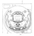
以下、実施例に基づいて本発明を詳細に説明する。図1は、本実施例のパチンコ機GMを示す斜視図である。このパチンコ機GMは、島構造体に着脱可能に装着される矩形枠状の木製外枠1と、外枠1に固着されたヒンジ2を介して開閉可能に枢着される前枠3とで構成されている。この前枠3には、遊技盤5が、裏側からではなく、表側から着脱自在に装着され、その前側には、ガラス扉6と前面板7とが夫々開閉自在に枢着されている。
Hereinafter, the present invention will be described in detail based on examples. FIG. 1 is a perspective view showing a pachinko machine GM of the present embodiment. This pachinko machine GM includes a rectangular frame-shaped wooden
ガラス扉6の外周には、LEDランプなどによる電飾ランプが、略C字状に配置されている。一方、ガラス扉6の上部左右位置と下側には、全3個のスピーカが配置されている。上部に配置された2個のスピーカは、各々、左右チャネルR,Lの音声を出力し、下側のスピーカは重低音を出力するよう構成されている。
On the outer periphery of the
前面板7には、発射用の遊技球を貯留する上皿8が装着され、前枠3の下部には、上皿8から溢れ出し又は抜き取った遊技球を貯留する下皿9と、発射ハンドル10とが設けられている。発射ハンドル10は発射モータと連動しており、発射ハンドル10の回動角度に応じて動作する打撃槌によって遊技球が発射される。
The
上皿8の外周面には、チャンスボタン11が設けられている。このチャンスボタン11は、遊技者の左手で操作できる位置に設けられており、遊技者は、発射ハンドル10から右手を離すことなくチャンスボタン11を操作できる。このチャンスボタン11は、通常時には機能していないが、ゲーム状態がボタンチャンス状態となると内蔵ランプが点灯されて操作可能となる。なお、ボタンチャンス状態は、必要に応じて設けられるゲーム状態である。
A
上皿8の右部には、カード式球貸し機に対する球貸し操作用の操作パネル12が設けられ、カード残額を3桁の数字で表示する度数表示部と、所定金額分の遊技球の球貸しを指示する球貸しスイッチと、ゲーム終了時にカードの返却を指令する返却スイッチとが設けられている。
On the right side of the
図2に示すように、遊技盤5の表面には、金属製の外レールと内レールとからなるガイドレール13が環状に設けられ、その略中央には、中央開口HOが設けられている。そして、中央開口HOには、大型の液晶カラーディスプレイ(LCD)で構成された表示装置DSが配置されている。
As shown in FIG. 2, a
表示装置DSは、大当り状態に係わる特定図柄を変動表示すると共に背景画像や各種のキャラクタなどをアニメーション的に表示する装置である。この表示装置DSは、中央部に特別図柄表示部Da〜Dcと右上部に普通図柄表示部19とを有している。そして、特別図柄表示部Da〜Dcでは、大当り状態の招来を期待させるリーチ演出が実行されることがあり、特別図柄表示部Da〜Dc及びその周りでは、適宜な予告演出などが実行される。
The display device DS is a device that variably displays a specific symbol related to the big hit state and displays a background image and various characters in an animated manner. This display device DS has special symbol display portions Da to Dc in the center portion and a normal
遊技球が落下移動する遊技領域には、図柄始動口15、大入賞口16、普通入賞口17、及び、ゲート18が配設されている。これらの入賞口15〜18は、それぞれ内部に検出スイッチを有しており、遊技球の通過を検出できるようになっている。
In the game area where the game ball falls and moves, a symbol start
図柄始動口15は、左右一対の開閉爪15aを備えた電動式チューリップで開閉されるように構成され、普通図柄表示部17の変動後の停止図柄が当り図柄を表示した場合には、所定時間だけ、若しくは、所定個数の遊技球を検出するまで、開閉爪15aが開放されるようになっている。
The symbol start
なお、普通図柄表示部19は、普通図柄を表示するものであり、ゲート18を通過した遊技球が検出されると、普通図柄が所定時間だけ変動し、遊技球のゲート18の通過時点において抽出された抽選用乱数値により決定される停止図柄を表示して停止する。
The normal
大入賞口16は、前後方向に進退する開閉板16aを有して構成されている。大入賞口16の動作は、特に限定されないが、典型的な大当り状態では、大入賞口16の開閉板16aが開放された後、所定時間が経過し、又は所定数(例えば10個)の遊技球が入賞すると開閉板16aが閉じる。このような動作は、最大で例えば15回まで継続され、遊技者に有利な状態に制御される。なお、特別図柄表示部Da〜Dcの変動後の停止図柄が特別図柄のうちの特定図柄であった場合には、特別遊技の終了後のゲームが高確率状態(確変状態)となるという特典が付与される。
The special winning
図3は、上記した各動作を実現するパチンコ機GMの全体回路構成を示すブロック図である。図示の通り、このパチンコ機GMは、AC24Vを受けて各種の直流電圧や、電源異常信号ABN1、ABN2やシステムリセット信号(電源リセット信号)SYSなどを出力する電源基板20と、遊技制御動作を中心統括的に担う主制御基板21と、主制御基板21から受けた制御コマンドCMDに基づいてランプ演出及び音声演出を実行する演出制御基板22と、演出制御基板22から受けた制御コマンドCMD’に基づいて表示装置DSを駆動する画像制御基板23と、主制御基板21から受けた制御コマンドCMD”に基づいて払出モータMを制御して遊技球を払い出す払出制御基板24と、遊技者の操作に応答して遊技球を発射させる発射制御基板25と、を中心に構成されている。
FIG. 3 is a block diagram showing an overall circuit configuration of the pachinko machine GM that realizes the above-described operations. As shown in the figure, this pachinko machine GM mainly receives a 24V AC and outputs various DC voltages, power supply abnormality signals ABN1, ABN2, a system reset signal (power reset signal) SYS, and the like, and a game control operation. Based on the
但し、この実施例では、主制御基板21が出力する制御コマンドCMDは、コマンド中継基板26と演出インタフェイス基板27を経由して、演出制御基板22に伝送される。また、演出制御基板22が出力する制御コマンドCMD’は、演出インタフェイス基板27と画像インタフェイス基板28を経由して、画像制御基板23に伝送され、主制御基板21が出力する制御コマンドCMD”は、主基板中継基板32を経由して、払出制御基板24に伝送される。制御コマンドCMD,CMD’,CMD”は、何れも16ビット長であるが、主制御基板21や払出制御基板24が関係する制御コマンドは、8ビット長毎に2回に分けてパラレル送信されている。一方、演出制御基板22から画像制御基板23に伝送される制御コマンドCMD’は、16ビット長をまとめてパラレル伝送されている。そのため、可動予告演出を含む予告演出を、多様化して多数の制御コマンドを連続的に送受信するような場合でも、迅速にその処理を終えることができ、他の制御動作に支障を与えない。
However, in this embodiment, the control command CMD output from the
ところで、本実施例では、演出インタフェイス基板27と演出制御基板22とは、配線ケーブルを経由することなく、雄型コネクタと雌型コネクタとを直結されて二枚の回路基板が積層されている。同様に、画像インタフェイス基板28と画像制御基板23についても、配線ケーブルを経由することなく、雄型コネクタと雌型コネクタとを直結されて二枚の回路基板が積層されている。そのため、各電子回路の回路構成を複雑高度化しても基板全体の収納空間を最小化できると共に、接続ラインを最短化することで耐ノイズ性を高めることができる。
By the way, in the present embodiment, the
これら主制御基板21、演出制御基板22、画像制御基板23、及び払出制御基板24には、ワンチップマイコンを備えるコンピュータ回路がそれぞれ搭載されている。そこで、これらの制御基板21〜24とインタフェイス基板27〜28に搭載された回路、及びその回路によって実現される動作を機能的に総称して、本明細書では、主制御部21、演出制御部22’、画像制御部23’、及び払出制御部24と言うことがある。すなわち、この実施例では、演出制御基板22と演出インタフェイス基板27とで演出制御部22’を構成し、画像制御基板23と画像インタフェイス基板28とで画像制御部23’を構成している。なお、演出制御部22’、画像制御部23’、及び払出制御部24の全部又は一部がサブ制御部である。
The
また、このパチンコ機GMは、図3の破線で囲む枠側部材GM1と、遊技盤5の背面に固定された盤側部材GM2とに大別されている。枠側部材GM1には、ガラス扉6や前面板7が枢着された前枠3と、その外側の木製外枠1とが含まれており、機種の変更に拘わらず、長期間にわたって遊技ホールに固定的に設置される。一方、盤側部材GM2は、機種変更に対応して交換され、新たな盤側部材GM2が、元の盤側部材の代わりに枠側部材GM1に取り付けられる。なお、枠側部材1を除く全てが、盤側部材GM2である。
The pachinko machine GM is roughly divided into a frame side member GM1 surrounded by a broken line in FIG. 3 and a board side member GM2 fixed to the back of the
図3の破線枠に示す通り、枠側部材GM1には、電源基板20と、払出制御基板24と、発射制御基板25と、枠中継基板35と、ランプ駆動基板36とが含まれており、これらの回路基板が、前枠3の適所に各々固定されている。
As shown in the broken line frame in FIG. 3, the frame side member GM1 includes a
ランプ駆動基板36には、複数のLEDが接続されており、これらのLED群を駆動する駆動データSDATAは、シリアル信号として、演出制御基板22→演出インタフェイス基板27→枠中継基板34→枠中継基板35を経由して、ランプ駆動基板36に搭載された複数のドライバDRijに伝送されている。
A plurality of LEDs are connected to the
実施例のドライバDRij(ドライバIC)は、各々、LEDや電飾ランプなどのLED群を最高24個まで駆動可能であるが、以下の説明では、ランプ駆動基板36に搭載された5個のドライバDRijによって、合計5×24個のLEDが駆動されているとする(図7参照)。そして、本明細書では、これらのLEDを、便宜上、第0チャンネル(CH0)のLED群と称する。
Each of the drivers DRij (driver ICs) of the embodiment can drive up to 24 LED groups such as LEDs and electric lamps, but in the following description, five drivers mounted on the
遊技盤5の背面には、主制御基板21、演出制御基板22、画像制御基板23が、表示装置DSやその他の回路基板と共に固定されている。そして、枠側部材GM1と盤側部材GM2とは、一箇所に集中配置された接続コネクタC1〜C4によって電気的に接続されている。
On the back surface of the
電源基板20は、接続コネクタC2を通して、主基板中継基板32に接続され、接続コネクタC3を通して、電源中継基板33に接続されている。電源基板20には、交流電源の投入と遮断とを監視する電源監視部MNTが設けられている。電源監視部MNTは、交流電源が投入されたことを検知すると、所定時間だけシステムリセット信号SYSをLレベルに維持した後に、これをHレベルに遷移させる。
The
また、電源監視部MNTは、交流電源の遮断を検知すると、電源異常信号ABN1,ABN2を、直ちにLレベルに遷移させる。なお、電源異常信号ABN1,ABN2は、電源投入後に速やかにHレベルとなる。 Further, when power supply monitoring unit MNT detects the interruption of the AC power supply, power supply abnormality signals ABN1 and ABN2 are immediately shifted to the L level. The power supply abnormality signals ABN1 and ABN2 quickly become H level after the power is turned on.
ところで、本実施例のシステムリセット信号は、交流電源に基づく直流電源によって生成されている。そのため、交流電源の投入(通常は電源スイッチのON)を検知してHレベルに増加した後は、直流電源電圧が異常レベルまで低下しない限り、Hレベルを維持する。したがって、直流電源電圧が維持された状態で、交流電源が瞬停状態となっても、システムリセット信号SYSがCPUをリセットすることはない。なお、電源異常信号ABN1,ABN2は、交流電源の瞬停状態でも出力される。 Incidentally, the system reset signal of this embodiment is generated by a DC power supply based on an AC power supply. For this reason, after detecting the turning-on of the AC power supply (usually turning on the power switch) and increasing it to the H level, the H level is maintained unless the DC power supply voltage drops to an abnormal level. Therefore, even if the AC power supply is in an instantaneous power interruption state while the DC power supply voltage is maintained, the system reset signal SYS does not reset the CPU. The power supply abnormality signals ABN1 and ABN2 are also output even when the AC power supply is instantaneously stopped.
主基板中継基板32は、電源基板20から出力される電源異常信号ABN1、バックアップ電源BAK、及びDC5V,DC12V,DC32Vを、そのまま主制御部21に出力している。一方、電源中継基板33は、電源基板20から受けたシステムリセット信号SYSや、交流及び直流の電源電圧を、そのまま演出インタフェイス基板27に出力している。演出インタフェイス基板27は、受けたシステムリセット信号SYSを、そのまま演出制御部22’と画像制御部23’に出力している。
The main
一方、払出制御基板24は、中継基板を介することなく、電源基板20に直結されており、主制御部21が受けると同様の電源異常信号ABN2や、バックアップ電源BAKを、その他の電源電圧と共に直接的に受けている。
On the other hand, the
電源基板20が出力するシステムリセット信号SYSは、電源基板20に交流電源24Vが投入されたことを示す電源リセット信号であり、この電源リセット信号によって演出制御部22’と画像制御部23’のワンチップマイコンは、その他のIC素子と共に電源リセットされるようになっている。
The system reset signal SYS output from the
但し、このシステムリセット信号SYSは、主制御部21と払出制御部24には、供給されておらず、各々の回路基板21,24のリセット回路RSTにおいて電源リセット信号(CPUリセット信号)が生成されている。そのため、例えば、接続コネクタC2がガタついたり、或いは、配線ケーブルにノイズが重畳しても、主制御部21や払出制御部24のCPUが異常リセットされるおそれはない。演出制御部22’と画像制御部23’は、主制御部21からの制御コマンドに基づいて、従属的に演出動作を実行することから、回路構成の複雑化を回避するために、電源基板20から出力されるシステムリセット信号SYSを利用している。
However, the system reset signal SYS is not supplied to the
ところで、主制御部21や払出制御部24に設けられたリセット回路RSTは、各々ウォッチドッグタイマを内蔵しており、各制御部21,24のCPUから、定時的なクリアパルスを受けない限り、各CPUは強制的にリセットされる。
By the way, the reset circuits RST provided in the
また、この実施例では、RAMクリア信号CLRは、主制御部21で生成されて主制御部21と払出制御部24のワンチップマイコンに伝送されている。ここで、RAMクリア信号CLRは、各制御部21,24のワンチップマイコンの内蔵RAMの全領域を初期設定するか否かを決定する信号であって、係員が操作する初期化スイッチSWのON/OFF状態に対応した値を有している。
In this embodiment, the RAM clear signal CLR is generated by the
主制御部21及び払出制御部24は、電源基板20から電源異常信号ABN1,ABN2を受けることによって、停電や営業終了に先立って、必要な終了処理を開始するようになっている。また、バックアップ電源BAKは、営業終了や停電により交流電源24Vが遮断された後も、主制御部21と払出制御部24のワンチップマイコンの内蔵RAMのデータを保持するDC5Vの直流電源である。したがって、主制御部21と払出制御部24は、電源遮断前の遊技動作を電源投入後に再開できることになる(電源バックアップ機能)。このパチンコ機では少なくとも数日は、各ワンチップマイコンのRAMの記憶内容が保持されるよう設計されている。
The
図3に示す通り、主制御部21は、主基板中継基板32を経由して、払出制御部24に制御コマンドCMD”を送信する一方、払出制御部24からは、遊技球の払出動作を示す賞球計数信号や、払出動作の異常に係わるステイタス信号CONや、動作開始信号BGNを受信している。ステイタス信号CONには、例えば、補給切れ信号、払出不足エラー信号、下皿満杯信号が含まれる。動作開始信号BGNは、電源投入後、払出制御部24の初期動作が完了したことを主制御部21に通知する信号である。
As shown in FIG. 3, the
また、主制御部21は、遊技盤中継基板31を経由して、遊技盤5の各遊技部品に接続されている。そして、遊技盤上の各入賞口16〜18に内蔵された検出スイッチのスイッチ信号を受ける一方、電動式チューリップなどのソレノイド類を駆動している。ソレノイド類や検出スイッチは、主制御部21から配電された電源電圧VB(12V)で動作するよう構成されている。また、図柄始動口15への入賞状態などを示す各スイッチ信号は、電源電圧VB(12V)と電源電圧Vcc(5V)とで動作するインタフェイスICで、TTLレベル又はCMOSレベルのスイッチ信号に変換された上で、主制御部21に伝送される。
The
先に説明した通り、演出制御基板22と演出インタフェイス基板27とはコネクタ連結によって一体化されており、演出制御部22’は、電源中継基板33を経由して、電源基板20から各レベルの直流電圧(5V,12V,32V)と、システムリセット信号SYSを受けている(図3及び図4参照)。また、演出制御部22’は、コマンド中継基板26を経由して、主制御部21から制御コマンドCMDとストローブ信号STBとを受けている(図3及び図4参照)。
As described above, the
そして、演出制御部22’は、演出インタフェイス基板27を経由して、ランプ駆動基板29やランプ駆動基板30に搭載されたドライバDRijに、ランプ駆動データSDATA(シリアル信号)を供給している。特に限定されるものではないが、ランプ駆動基板29,30に搭載されているドライバDRijは、ランプ駆動基板36に搭載されたドライバDRijと同一構成であり、ランプ駆動基板29,30には、各々、5個のドライバDRijが配置されている。
The
先に説明した通り、これらのドライバDRijは、各々、最高24個のランプを駆動可能であるが、以下の説明では、ランプ駆動基板29に接続された合計24×5個のランプを、第1チャンネルCH1のランプ群と称し、ランプ駆動基板30に接続された合計24×5個のランプを、第2チャンネルCH2のランプ群と称することがある。
As described above, each of these drivers DRij can drive a maximum of 24 lamps. In the following description, a total of 24 × 5 lamps connected to the
このように、本実施例では、多数(3×24×5個)のランプが、チャンネルCH0〜チャンネルCH2のランプ群に三分されて、各々、ランプ駆動基板36、ランプ駆動基板29、ランプ駆動基板30に接続されている。なお、全てのドライバDRijは、演出制御部22’のワンチップマイコン40が、一括的に出力するシリアル信号SDATAのうち、該当信号を受信して、担当するランプ群を駆動している(図4参照)。
As described above, in this embodiment, a large number (3 × 24 × 5) of lamps are divided into three groups of lamps of channel CH0 to channel CH2, respectively, and the
ところで、同じドライバDRijを使用してステッピングモータを駆動することもでき、例えば、破線に示すように、ランプ駆動基板30を経由して、演出モータ群M1〜Mnを駆動するのも好適である。この場合、モータ駆動データは、ランプ駆動データと同様のシリアル信号であり、演出内容を豊富化するべく演出モータ個数を増やしても、配線ケーブルが増加することがなく、機器構成が簡素化される。
By the way, it is possible to drive the stepping motor using the same driver DRij. For example, it is also preferable to drive the effect motor groups M1 to Mn via the
図3及び図4に示す通り、演出制御部22’は、画像制御部23’に対して、制御コマンドCMD’及びストローブ信号STB’と、電源基板20から受けたシステムリセット信号SYSと、2種類の直流電圧(12V,5V)とを出力している。
As shown in FIGS. 3 and 4, the
そして、画像制御部23’では、制御コマンドCMD’に基づいて表示装置DSを駆動して各種の画像演出を実行している。表示装置DSは、LEDバックライトによって発光しており、画像インタフェイス基板28から5対のLVDS(低電圧差動伝送Low voltage differential signaling)信号と、バックライト電源電圧(12V)とを受けて駆動されている(図4参照)。
Then, the image controller 23 'drives the display device DS based on the control command CMD' to execute various image effects. The display device DS emits light by an LED backlight, and is driven by receiving five pairs of LVDS (Low voltage differential signaling) signals and a backlight power supply voltage (12 V) from the
続いて、上記した演出制御部22’と画像制御部23’の構成を更に詳細に説明する。図4に示す通り、演出インタフェイス基板27は、電源中継基板33を経由して、電源基板20から3種類の直流電圧(5V,12V,32V)を受けている。ここで、直流電圧5Vは、デジタル論理回路の電源電圧として、演出インタフェイス基板27、ランプ駆動基板29、ランプ駆動基板30、画像インタフェイス基板28、及び画像制御基板23に配電されて各デジタル回路を動作させている。
Next, the configurations of the effect control unit 22 'and the image control unit 23' will be described in more detail. As shown in FIG. 4, the
但し、演出制御基板22には、直流電圧5Vが配電されておらず、12VからDC/DCコンバータで降圧された直流電圧3.3Vと、3.3VからDC/DCコンバータで更に降圧された直流電圧1.8Vだけが、演出インタフェイス基板27から演出制御基板22に配電されている。
However, the direct
このように、本実施例の演出制御基板22は、全ての回路が、電源電圧3.3V又はそれ以下の電源電圧で駆動されているので、電源電圧を5Vで動作する場合と比較して大幅に低電力化することができ、仮に、演出制御基板22の直上に演出インタフェイス基板27を配置して積層しても放熱上の問題が生じない。
In this way, the
但し、電源基板20から受けた直流電圧12Vは、そのままデジタルアンプ46の電源電圧として使用されると共に、ランプ駆動基板30とランプ駆動基板29に配電されて各ランプ群の電源電圧となる。また、直流電圧32Vは、演出インタフェイス基板のDC/DCコンバータにおいて直流電圧13Vに降圧されて、必要に応じて、演出モータM1〜Mnの駆動電源として使用される。
However, the
図4に示すように、演出制御部22’は、音声演出・ランプ演出・演出可動体による予告演出・データ転送などの処理を実行するワンチップマイコン40と、ワンチップマイコン40の制御プログラムなどを記憶する不揮発性メモリ41と、ワンチップマイコン40からの指示に基づいて音声信号を再生して出力する音声合成回路42と、再生される音声信号の元データである圧縮音声データを記憶する音声用メモリ43と、ワンチップマイコン40の動作タイミングを規定するシステムクロックSCKを生成するクロック発振部39と、を備えて構成されている。
As shown in FIG. 4, the
なお、ワンチップマイコン40、フラッシュメモリ41、及び音声用メモリ43は、電源電圧3.3Vで動作しており、また、音声合成回路42は、電源電圧3.3V及び電源電圧1.8Vで動作しており大幅な省電力化が実現されている。1.8Vは、音声合成回路のコンピュータ・コア部の電源電圧であり、3.3Vは、I/O部の電源電圧である。
The one-
ところで、本実施例のクロック発振部39は、水晶振動子Xtalの固有周波数で規定される中心周波数Fiを固定的に発振するのではなく、中心周波数Fiを中心として、所定範囲内で周波数(Fi−δ〜Fi+δ)が偏移するシステムクロックSCK(変調クロック)を生成している。なお、周波数偏移量δは、中心周波数Fiの上下に±1.0%程度とするか(センタスプレッド)、或いは、中心周波数Fiの上方又は下方に0〜2.0%程度とするのが好適である(アップスプレッド又はダウンスプレッド)。 Incidentally, the clock oscillating unit 39 of this embodiment does not oscillate fixedly the center frequency Fi defined by the natural frequency of the crystal resonator Xtal, but has a frequency (Fi within a predetermined range with the center frequency Fi as the center. A system clock SCK (modulation clock) in which (−δ to Fi + δ) shifts is generated. The frequency shift amount δ is about ± 1.0% above and below the center frequency Fi (center spread), or about 0 to 2.0% above or below the center frequency Fi. Preferred (up spread or down spread).
図5(a)は、その回路構成を例示したものであり、水晶振動子Xtalによる原発振回路OSCと、原発振回路OSCの発振周波数Fiを偏移させる周波数変調回路FSと、を有して構成されている。原発振回路OSCは、水晶振動子Xtalと、インバータINと、帰還抵抗Rsと、負荷コンデンサC11,C12とを有して構成され、中心周波数Fiの基準クロックを生成している。ここで、インバータINと帰還抵抗Rsを接続する正帰還ループは、制御信号CTLによって開閉制御可能に構成されており、制御信号CTLによって発振動作の許否が制御可能に構成されている。 FIG. 5A illustrates the circuit configuration, and includes an original oscillation circuit OSC using a crystal resonator Xtal and a frequency modulation circuit FS that shifts the oscillation frequency Fi of the original oscillation circuit OSC. It is configured. The original oscillation circuit OSC includes a crystal resonator Xtal, an inverter IN, a feedback resistor Rs, and load capacitors C11 and C12, and generates a reference clock having a center frequency Fi. Here, the positive feedback loop connecting the inverter IN and the feedback resistor Rs is configured to be open / close controlled by the control signal CTL, and is configured to be able to control whether the oscillation operation is permitted by the control signal CTL.
なお、図5(a)では、信号端子Xin,Xout間に、水晶振動子Xtalを接続して自励発振させる構成を示しているが、図5(c)に示すように、信号端子Xoutを解放状態にすれば、他の回路から受ける外部クロックを周波数変調することも可能となる。なお、この場合には、基準クロックは、外部クロックを論理否定した論理レベルとなる。 FIG. 5A shows a configuration in which a crystal resonator Xtal is connected between the signal terminals Xin and Xout to cause self-excited oscillation. However, as shown in FIG. In the released state, the external clock received from another circuit can be frequency-modulated. In this case, the reference clock has a logic level obtained by logically negating the external clock.
周波数変調回路FSは、PLL(phase locked loop )動作を実行するPLLブロック37と、そのPLL動作を制御する制御端子T1,T2とを有して構成されている。そして、制御端子T1にHレベルの制御信号を受けると、原発振回路OSCとPLLブロック37の動作が許可される。また、制御端子T2に受ける設定信号の論理レベルに応じて、変調度が高低に設定可能となっている。変調度は、中心周波数Fiからの周波数偏移量を意味し、制御端子T2が受ける設定信号の論理レベルに応じて、例えば、±0.5%か、±1.0%かの何れかの周波数偏移量となる。なお、図示例では、設定信号がHレベル(変調度が高レベル)であって、周波数偏移量が±1.0%となっている。
The frequency modulation circuit FS includes a
但し、必ずしも、センタスプレッド方式によって中心周波数Fiの上下に周波数変調する必要はなく、制御端子T2が受ける設定信号の論理レベルに応じて、例えば、中心周波数Fiの下方に−1.0%か、−2.0%かの何れかの周波数偏移量とするダウンスプレッド方式を採っても良い。 However, it is not always necessary to perform frequency modulation above and below the center frequency Fi by the center spread method, for example, −1.0% below the center frequency Fi, depending on the logic level of the setting signal received by the control terminal T2. A down spread method in which any frequency shift amount of −2.0% may be adopted.
何れにしても、PLLブロック37から出力されるシステムクロックSCKは、δ=Fi×2/100程度、その周波数が偏移するので、不要輻射ノイズEMIの抑制に効果的に寄与する。なお、この点は、ランプ駆動信号やモータ駆動信号に関して更に後述する。
In any case, since the frequency of the system clock SCK output from the
図5(b)は、PLLブロック37の内部構成を図示したものであり、変調ロジック部59を除けば、通常のPLL回路とほぼ同様である。すなわち、PLLブロック37は、変調ロジック部59の他に、出力信号(変調クロック出力)を1/M分周する第1分周部50と、基準クロックを1/N分周する第2分周部51と、基準クロックを1/L分周する第3分周部52と、第1分周部50と第2分周部51の出力を比較する位相比較部53と、位相比較部53の出力を受けるチャージポンプ54と、抵抗とコンデンサによるループフィルタ55と、ループフィルタ55の出力電圧に対応して出力周波数Foが変化する電圧制御発振部VCOと、を有して構成されている。
FIG. 5B illustrates the internal configuration of the
但し、PLLブロック37は、通常のPLL回路とは異なり、変調ロジック部59から受ける変調信号MDに基づいて、電圧制御発振部VCOの周波数が、最大で2%程度、微小に揺らぐ周波数変調が実現されるよう構成されている。また、実施例では、変調周期を、時間的に切り替え、変調周期τ1でVCOの出力周波数をFo−δ〜Fo+δの範囲で変化させた後、変調周期τ2でVCOの出力周波数をFo−δ〜Fo+δの範囲で変化させている。その結果、出力周波数が更に不規則に周波数変調されることで、不要輻射ノイズEMIの抑制効果が高まる。
However, unlike a normal PLL circuit, the
何れにしても、PLLブロック37内部では、周波数Fo/Mの第1分周部50の出力信号と、周波数Fi/Nの第2分周部51の出力信号との位相差が、位相比較器53において検出され、その位相差がゼロとなるよう負帰還ループが機能するので、Fo/M=Fi/Nの関係が成立し、出力信号(変調クロック出力)の周波数Foは、やや揺らぐもののFo=Fi×M/Nとなる。本実施例では、この出力信号が、システムクロックSCKとしてワンチップマイコン40に供給され、ワンチップマイコン40の内部動作の動作タイミングを規定している。
In any case, in the
このようなシステムクロックSCKに基づいて動作するワンチップマイコン40には、複数のパラレル入出力ポートPIO(Pi+Po+Po’)と、複数のシリアル出力ポートSIとが内蔵されている。ここで、シリアル出力ポートSIは、より詳細には、3チャンネルのシリアルポート(S0〜S2)を含んで構成されており(図6参照)、ランプ駆動基板36、29、30に搭載された各5個のドライバDRijに、各々、ランプ駆動データSDATA0〜SDATA2を、クロック信号CK0〜CK2に同期して出力している。
The one-
すなわち、シリアルポートS0〜シリアルポートS2は、クロック同期方式に基づいて、対応するランプ駆動基板36、29、30に、ランプ駆動データSDATA0〜SDATA2を伝送している。なお、ランプ駆動データSDATA0〜SDATA2は、各LEDの発光輝度をPWM制御(pulse width modulation)によって輝度調整するため輝度データである。
That is, the serial port S0 to serial port S2 transmit the lamp drive data SDATA0 to SDATA2 to the corresponding
また、ランプ駆動基板36、29、30は、パラレル入出力ポートPIOのパラレル出力ポートPo’にも接続されており、各ランプ駆動基板36、29、30に搭載されたドライバDRijは、パラレル出力ポートPo’が出力する3ビット長の動作許可信号ENABLE0〜ENABLE2の何れかに基づいて動作を開始している。
The
一方、パラレル入出力ポートPIOの入力ポートPiには、主制御部21からの制御コマンドCMD及びストローブ信号STBが入力され、コマンド出力ポートPoからは、制御コマンドCMD’及びストローブ信号STB’が出力されるよう構成されている。
On the other hand, the control command CMD and the strobe signal STB from the
具体的には、入力ポートPiには、主制御基板21から出力された制御コマンドCMDとストローブ信号(割込み信号)STBとが、演出インタフェイス基板27のバッファ44において、電源電圧3.3Vに対応する論理レベルに変換されて8ビット単位で供給される。割込み信号STBは、ワンチップマイコンの割込み端子に供給され、受信割込み処理によって、演出制御部22’は、制御コマンドCMDを取得するよう構成されている。
Specifically, a control command CMD and a strobe signal (interrupt signal) STB output from the
演出制御部22’が取得する制御コマンドCMDには、(1)異常報知その他の報知用制御コマンドなどの他に、(2)図柄始動口への入賞に起因する各種演出動作の概要特定する制御コマンド(変動パターンコマンド)や、図柄種別を指定する制御コマンド(図柄指定コマンド)が含まれている。ここで、変動パターンコマンドで特定される演出動作の概要には、演出開始から演出終了までの演出総時間と、大当たり抽選における当否結果とが含まれている。
The control command CMD acquired by the
また、図柄指定コマンドには、大当たり抽選の結果に応じて、大当たりの場合には、大当たり種別に関する情報(15R確変、2R確変、15R通常、2R通常など)を特定する情報が含まれ、ハズレの場合には、ハズレを特定する情報が含まれている。変動パターンコマンドで特定される演出動作の概要には、演出開始から演出終了までの演出総時間と、大当り抽選における当否結果とが含まれている。なお、これらに加えて、リーチ演出や予告演出の有無などを含めて変動パターンコマンドで特定しても良いが、この場合でも、演出内容の具体的な内容は特定されていない。 In addition, the symbol designating command includes information for identifying information on the jackpot type (15R probability variation, 2R probability variation, 15R normal, 2R normal, etc.) in the case of a jackpot according to the result of the jackpot lottery. In some cases, information for identifying a loss is included. The outline of the production operation specified by the variation pattern command includes the production total time from the production start to the production end, and the result of success or failure in the big hit lottery. In addition to these, the change pattern command including the presence or absence of the reach effect or the notice effect may be specified, but even in this case, the specific content of the effect content is not specified.
そのため、演出制御部22’では、変動パターンコマンドを取得すると、これに続いて演出抽選を行い、取得した変動パターンコマンドで特定される演出概要を更に具体化している。例えば、リーチ演出や予告演出について、その具体的な内容が決定される。そして、決定された具体的な遊技内容にしたがい、LED群などの点滅によるランプ演出や、スピーカによる音声演出の準備動作を行うと共に、画像制御部23’に対して、ランプやスピーカによる演出動作に同期した画像演出に関する制御コマンドCMD’を出力する。
Therefore, when the change pattern command is acquired, the
このような演出動作に同期した画像演出を実現するため、演出制御部22’は、コマンド出力ポートPoを通して、画像制御部23’に対するストローブ信号(割込み信号)STB’と共に、16ビット長の制御コマンドCMD’を演出インタフェイス基板27に向けて出力している。なお、演出制御部22’は、図柄指定コマンドや、表示装置DSに関連する報知用制御コマンドや、その他の制御コマンドを受信した場合は、その制御コマンドを、16ビット長に纏めた状態で、割込み信号STB’と共に演出インタフェイス基板27に向けて出力している。
In order to realize such an image effect synchronized with the effect operation, the
上記した演出制御基板22の構成に対応して、演出インタフェイス基板27には出力バッファ45が設けられており、16ビット長の制御コマンドCMD’と1ビット長の割込み信号STB’を画像インタフェイス基板28に出力している。そして、これらのデータCMD’,STB’は、画像インタフェイス基板28を経由して、画像制御基板23に伝送される。
Corresponding to the configuration of the
また、演出インタフェイス基板27には、音声合成回路42から出力される音声信号を受けるデジタルアンプ46が配置されている。先に説明した通り、音声合成回路42は、3.3Vと1.8Vの電源電圧で動作しており、また、デジタルアンプ46は、電源電圧12VでD級増幅動作しており、消費電力を抑制しつつ大音量の音声演出を可能にしている。
The
そして、デジタルアンプ46の出力によって、遊技機上部の左右スピーカと、遊技機下部のスピーカとを駆動している。そのため、音声合成回路42は、3チャネルの音声信号を生成する必要があり、これをパラレル伝送すると、音声合成回路42とデジタルアンプ46との配線が複雑化する。
The left and right speakers at the upper part of the gaming machine and the speakers at the lower part of the gaming machine are driven by the output of the digital amplifier 46. Therefore, the
そこで、本実施例では、音質の劣化を防止すると共に、配線の複雑化を回避するため、音声合成回路42とデジタルアンプ46との間は、4本の信号線で接続されており、具体的には、転送クロック信号SCLKと、チャネル制御信号LRCLKと、2ビット長のシリアル信号SD1,SD2との合計4ビットの信号線に抑制されている。なお、何れの信号も、その振幅レベルは3.3Vである。
Therefore, in this embodiment, the
ここで、SD1は、遊技機上部に配置された左右スピーカのステレオ信号R,Lを特定するPCMデータについてのシリアル信号であり、SD2は、遊技機下部に配置された重低音スピーカのモノラル信号を特定するPCMデータについてのシリアル信号である。そして、音声合成回路342は、チャネル制御信号LRCLKをLレベルに維持した状態で、左チャネルの音声信号Lを伝送し、チャネル制御信号LRCLKをHレベルに維持した状態で、右チャネルの音声信号Rを伝送する。なお、重低音スピーカは本実施例では1個であるので、モノラル音声信号が伝送されているが、ステレオ音声信号として伝送できるのは勿論である。 Here, SD1 is a serial signal for PCM data specifying the stereo signals R and L of the left and right speakers arranged at the upper part of the gaming machine, and SD2 is a monaural signal of the heavy bass speaker arranged at the lower part of the gaming machine. This is a serial signal for the PCM data to be specified. The voice synthesis circuit 342 transmits the left channel audio signal L while maintaining the channel control signal LRCLK at the L level, and maintains the channel control signal LRCLK at H level while maintaining the channel control signal LRCLK at the L level. Is transmitted. Note that since there is only one heavy bass speaker in this embodiment, a monaural audio signal is transmitted, but it is of course possible to transmit it as a stereo audio signal.
何れにしても本実施例では、4種類の音声信号を4本のケーブルで伝送可能であるので、最小のケーブル本数によってノイズによる音声劣化のない信号伝達が可能となる。すなわち、シリアル伝送であるのでパラレル伝送より圧倒的にケーブル本数が少な。なお、アナログ伝送を採る場合には、ケーブル本数は同数であるが、3.3V振幅のアナログ信号に、少なからずノイズが重畳して、音質が大幅に劣化する。一方、振幅レベルを上げると、電源配線が複雑化する上に消費電力が増加する。 In any case, in this embodiment, four types of audio signals can be transmitted with four cables, and therefore, signal transmission without audio deterioration due to noise can be performed with the minimum number of cables. That is, since it is serial transmission, the number of cables is far smaller than that of parallel transmission. Note that when analog transmission is employed, the number of cables is the same, but noise is superimposed on an analog signal having an amplitude of 3.3 V, and the sound quality is greatly deteriorated. On the other hand, when the amplitude level is increased, the power supply wiring becomes complicated and the power consumption increases.
このようなシリアル信号SD1,SD2は、クロック信号SCLKの立上りエッジに同期して、デジタルアンプ46に取得される。そして、デジタルアンプ46内部で、所定ビット長毎にパラレル変換され、DA変換後にD級増幅されて各スピーカに供給されている。 Such serial signals SD1 and SD2 are acquired by the digital amplifier 46 in synchronization with the rising edge of the clock signal SCLK. In the digital amplifier 46, parallel conversion is performed for each predetermined bit length, and after D / A conversion, D-class amplification is performed and supplied to each speaker.
本実施例では、音声合成回路42とデジタルアンプ46とをシリアル回線で接続するので、PCMデータ(音声データ)のビット長を如何に増やして高音質化を実現しても配線ケーブルその他を変更する必要がなく、回路構成の簡素化を維持することができる。
In this embodiment, since the
また、演出インタフェイス基板27には、ワンチップマイコン40のパラレル出力ポートPo’や、シリアルポートSIや出力される各種の信号を伝送する出力バッファ回路47,48,49が設けられている。ここで、出力バッファ47は、第0チャンネルのLED群に関連しており、ワンチップマイコン40が出力するランプ駆動データSDATA0、クロック信号CK0、及び、動作許可信号ENABLE0を、枠中継基板34に出力している。そして、出力された3ビットの信号は、枠中継基板34、及び、枠中継基板35を経由して、ランプ駆動基板36のドライバDRijに伝送される。
The
同様に、出力バッファ48は、ワンチップマイコン40が出力するランプ駆動データSDATA1、クロック信号CK1、及び、動作許可信号ENABLE1をランプ駆動基板29のドライバDRijに伝送しており、出力バッファ49は、ランプ駆動データSDATA2、クロック信号CK2、及び、動作許可信号ENABLE2をランプ駆動基板30のドライバDRijに伝送している。なお、ランプ駆動基板29のドライバDRijは、第1チャンネルのLED群を駆動し、ランプ駆動基板30のドライバDRijは、第2チャンネルのLED群を駆動している。
Similarly, the
図6(a)は、ワンチップマイコン40に内蔵されたシリアルポートSIの内部構成を図示したものである。図示の通り、シリアルポートS0〜シリアルポートS2は全ての同一構成であり、クロック同期方式のシリアル送受信動作が実現可能に構成されている。
FIG. 6A illustrates the internal configuration of the serial port SI built in the one-
そして、何れのシリアルポートSIも、CPUコアから1バイトデータを受ける送信データレジスタDRと、送信データレジスタDRから1バイトデータの転送を受けて、ランプ駆動データSDATAiとしてシリアル出力する送信シフトレジスタSRと、シリアルポートの内部動作状態を管理する多数の制御レジスタRGと、カウンタ回路CTの出力パルスΦを受けて制御レジスタRGが指定する分周比のクロック信号CKiを出力するボーレートジェネレータBGと、を有して構成されている。 Each serial port SI includes a transmission data register DR that receives 1-byte data from the CPU core, a transmission shift register SR that receives 1-byte data from the transmission data register DR, and serially outputs the data as lamp drive data SDATAi. And a number of control registers RG for managing the internal operation state of the serial port, and a baud rate generator BG for receiving the output pulse Φ of the counter circuit CT and outputting a clock signal CKi having a frequency division ratio designated by the control register RG. Configured.
カウンタ回路CTの出力パルスΦは、システムクロックSCKを適宜に分周したものであり、本実施例では、その周波数が適宜に揺らいでいる。そのため、ボーレートジェネレータBGから出力されるクロック信号CKiも同様に揺らぎ、ランプ駆動データSDATAiについても、揺らいだクロック信号に同期して出力されることになる。 The output pulse Φ of the counter circuit CT is obtained by appropriately dividing the system clock SCK. In this embodiment, the frequency fluctuates appropriately. Therefore, the clock signal CKi output from the baud rate generator BG also fluctuates in the same manner, and the lamp drive data SDATAi is output in synchronization with the fluctuating clock signal.
そのため、シリアル伝送線が、不要輻射ノイズEMIの放射アンテナとして機能して、クロック信号CKiやランプ駆動データSDATAiの基本周波数成分、及び、その高調波成分が周囲に放射される場合でも、本実施例によれば、各周波数成分が適宜に揺らぐことで、周囲のコンピュータ電子素子に与える悪影響を効果的に低減することができる。 Therefore, even in the case where the serial transmission line functions as a radiation antenna for unnecessary radiation noise EMI and the fundamental frequency component of the clock signal CKi and the lamp driving data SDATAi and its harmonic component are radiated to the surroundings, this embodiment According to the above, it is possible to effectively reduce an adverse effect on surrounding computer electronic elements by appropriately swinging each frequency component.
すなわち、不要輻射ノイズをスペクトル分析した場合におけるクロック信号CKiの基本波及び高調波のピーク値が大幅に低減されるので、主制御部やその他の制御部のワンチップマイコンに悪影響を与える可能性が低減されると共に、遊技者の携帯コンピュータ機器に悪影響を与えるおそれも解消される。 That is, the peak value of the fundamental wave and the harmonics of the clock signal CKi in the case of spectrum analysis of unwanted radiation noise is greatly reduced, which may adversely affect the one-chip microcomputer of the main control unit and other control units. This reduces the risk of adverse effects on the player's portable computer device.
次に、シリアルポートSIの他の構成についても説明すると、制御レジスタRGには、エンプティビットEMPを含んだREAD可能な制御レジスタが含まれており、送信データレジスタDRが、新規データを受け入れ可能か否かを示している。すなわち、送信シフトレジスタSRの1バイトデータの送信が完了すると、エンプティビットEMPがHレベル(empty レベル)に遷移して、送信データレジスタDRに、新規データを書込むことができることが示される。したがって、CPUコアは、エンプティビットEMPがHレベルであることを確認した上で、新規データを送信データレジスタDRに書込むことになる。 Next, another configuration of the serial port SI will be described. The control register RG includes a control register that can be read including the empty bit EMP, and can the transmission data register DR accept new data? Indicates whether or not. That is, when transmission of 1-byte data in transmission shift register SR is completed, empty bit EMP changes to H level (empty level), indicating that new data can be written into transmission data register DR. Therefore, the CPU core writes new data to the transmission data register DR after confirming that the empty bit EMP is at the H level.
また、制御レジスタRGには、送信許可ビットTXEを含んだWRITE可能な制御レジスタが含まれており、CPUが送信許可ビットTXEをON(H)レベルに設定すると、シリアルポートの送信動作が許可され、OFFレベルに設定すると送信動作が禁止される。そこで、本実施例では、CPUは、送信処理の開始時に送信許可ビットTXEをON状態にセットし、送信処理の終了時に送信許可ビットTXEをOFFレベルにリセットしている。 The control register RG includes a WRITE control register including a transmission permission bit TXE. When the CPU sets the transmission permission bit TXE to the ON (H) level, the serial port transmission operation is permitted. When set to the OFF level, the transmission operation is prohibited. Therefore, in this embodiment, the CPU sets the transmission permission bit TXE to the ON state at the start of the transmission process, and resets the transmission permission bit TXE to the OFF level at the end of the transmission process.
図6(b)は、シリアルポートS0〜S2について、送信開始時の動作を示すタイムチャートである。図示の通り、シリアルポートS0〜S2が送信禁止状態(TXE=L)である場合や、送信データレジスタDRのデータがシリアル出力された後は、クロック信号CKが固定状態のHレベルである。また、送信データレジスタDRは空であり、エンプティビットEMPもHレベル(empty レベル)である。 FIG. 6B is a time chart showing the operation at the start of transmission for the serial ports S0 to S2. As shown in the figure, when the serial ports S0 to S2 are in the transmission prohibited state (TXE = L), or after the data of the transmission data register DR is serially output, the clock signal CK is at the fixed H level. The transmission data register DR is empty, and the empty bit EMP is also at the H level (empty level).
そして、CPUが送信許可ビットTXEをON状態(送信許可状態)にセットした後、送信データレジスタDRに1バイト目の送信データを書込むと、エンプティビットEMPがLレベルに遷移すると共に、その後、所定時間(τ)経過後に、1バイト目の送信データが送信シフトレジスタSRに転送されて、シリアル送信動作が開始される。 Then, after the CPU sets the transmission permission bit TXE to the ON state (transmission permission state) and then writes the first byte of transmission data to the transmission data register DR, the empty bit EMP transitions to the L level, and then After a predetermined time (τ) elapses, the first byte of transmission data is transferred to the transmission shift register SR, and the serial transmission operation is started.
また、送信データが送信シフトレジスタSRに転送されたことで、1ビット目のシリアル送信開始に対応して、その後は、エンプティビットEMPがHレベル(empty レベル)に遷移する。したがって、CPUは、HレベルのエンプティビットEMPを確認した上で、2バイト目の送信データを、送信データレジスタDRに書込むことになる。 Further, since the transmission data is transferred to the transmission shift register SR, the empty bit EMP transitions to the H level (empty level) thereafter in response to the start of serial transmission of the first bit. Therefore, after confirming the H level empty bit EMP, the CPU writes the second byte of transmission data into the transmission data register DR.
すると、送信データレジスタDRへのデータ書込み動作に対応して、エンプティビットEMPがLレベル(fullレベル)に遷移する。そして、その後、1バイト目の送信データが全て送信されると、送信データレジスタDRから送信シフトレジスタSRに2バイト目のデータが転送され、2バイト目のデータ送信が開始されて、エンプティビットEMPがHレベルに遷移する。 Then, in response to the data write operation to the transmission data register DR, the empty bit EMP transitions to the L level (full level). After that, when all the transmission data of the first byte is transmitted, the second byte of data is transferred from the transmission data register DR to the transmission shift register SR, and the data transmission of the second byte is started, and the empty bit EMP Transitions to the H level.
このエンプティビットEMPは、送信データレジスタDRへの3バイト目のデータ書込み動作に対応して、Lレベルに変化するが、図示のように、新規データの書き込みがない場合にはHレベルを維持する。また、全てのデータが送信された後は、クロック信号CKがHレベルを維持して変化しない。 The empty bit EMP changes to the L level in response to the data write operation of the third byte to the transmission data register DR. However, as shown in the figure, the empty bit EMP maintains the H level when no new data is written. . Further, after all the data is transmitted, the clock signal CK maintains the H level and does not change.
図7は、ランプ駆動基板36,29,30の回路構成を確認的に図示したものである。図示の通り、ランプ駆動基板36には、5個のドライバDR00,DR01・・・DR04が搭載されて、第0チャンネルのLED群(合計5×24個のLED)を点灯駆動している。同様に、ランプ駆動基板29には、5個のドライバDR10,DR11・・・DR14が搭載され、また、ランプ駆動基板30には、5個のドライバDR18,DR19・・・DR1Cが搭載されて、各々、第1チャンネルと第2チャンネルのLED群(合計5×24個のLED)を点灯駆動している。
FIG. 7 shows the circuit configuration of the
各ドライバDRijには、5ビットの付番端子が設けられており、この付番端子に固定的なデジタルデータが供給される回路構成を採ることで、各々スレーブアドレス(ポートアドレス)が一連に付番されている。すなわち、図示例の場合には、各ドライバ(DR00,DR01・・・DR04、DR10,DR11・・・DR14、DR18,DR19・・・DR1C)のスレーブアドレスは、16進数表示で、00H,01H・・・04H、10H,11H・・・14H、18H,19H・・・1CHとなる。 Each driver DRij is provided with a 5-bit numbering terminal. By adopting a circuit configuration in which fixed digital data is supplied to this numbering terminal, each slave address (port address) is assigned in series. It is numbered. That is, in the illustrated example, the slave address of each driver (DR 00 , DR 01 ... DR 04 , DR 10 , DR 11 ... DR 14 , DR 18 , DR 19 ... DR 1C ) is In hexadecimal notation, 00H, 01H... 04H, 10H, 11H... 14H, 18H, 19H.
各ランプ制御基板36,29,30のドライバDRijに、一連のスレーブアドレスを付番することで、各ドライバDRijに対する輝度データなどの設定処理を迅速化することができる。また、各ドライバDRijには、24個のLEDを駆動する点灯駆動信号のアナログレベルを各々規定可能な階調レジスタGR0〜GR23が内蔵されている。
By assigning a series of slave addresses to the drivers DRij of the
階調レジスタGRnは、各々、8ビット長の輝度データを記憶可能であり、LEDの輝度レベルを00H〜FFHまで256段階で設定することができる。 Each of the gradation registers GRn can store 8-bit long luminance data, and the luminance level of the LED can be set in 256 steps from 00H to FFH.
以上、ランプ駆動データについて説明したが、本実施例では、演出制御部22’のワンチップマイコン40が、周波数変調されたシステムクロックSCKに基づいて動作するので、不要輻射ノイズEMIの抑制効果は、モータ駆動データなど、他のシリアル信号に対しても全く同様に成立する。なお、シリアル送信であるか、シリアル受信かも問わない。また、不要輻射ノイズEMIの抑制効果は、クロック同期式を採用した高速シリアル伝送において顕著であるが、調歩同期式のシリアル伝送においても同様に成立する。
Although the lamp drive data has been described above, in this embodiment, the one-
しかも、シリアル伝送時に、クロック信号CKiと駆動データSDATAiに位相ずれが生じるおそれもない。 In addition, there is no possibility of phase shift between the clock signal CKi and the drive data SDATAi during serial transmission.
ところで、上記の実施例では、周波数変調されたシステムクロックSCKを使用する場合について説明したが、上記の構成に代え、或いは、上記の構成に加えて図8に示す回路構成を採るのも好適である。 In the above embodiment, the case where the frequency-modulated system clock SCK is used has been described, but it is also preferable to adopt the circuit configuration shown in FIG. 8 instead of the above configuration or in addition to the above configuration. is there.
図8は、シリアルポートSIから出力されるクロック信号CKiを、周波数変調回路FSに供給して、変調度2%以下で周波数変調する回路構成を示している。なお、図8では、設定信号がLレベル(変調度が低レベル)であって、周波数偏移量が±0.5%となっている。 FIG. 8 shows a circuit configuration in which the clock signal CKi output from the serial port SI is supplied to the frequency modulation circuit FS and frequency-modulated with a modulation degree of 2% or less. In FIG. 8, the setting signal is at the L level (modulation level is low), and the frequency shift amount is ± 0.5%.
周波数変調回路FSの内部構成は、基本的に、図5に示す通りであるが、信号端子Xoutは解放状態であり、シリアルポートSIから出力されるクロック信号CKiは、周波数変調回路FSの信号端子Xinに供給されている。 The internal configuration of the frequency modulation circuit FS is basically as shown in FIG. 5, but the signal terminal Xout is in the released state, and the clock signal CKi output from the serial port SI is the signal terminal of the frequency modulation circuit FS. It is supplied to Xin.
また、図8に示す回路構成では、分周部50〜53の分周比(1/M,1/N,1/L)は、全て1に設定されている。そのため、信号端子Xinに供給されたクロック信号CKiは、逓倍比1の変調クロックCKi’に周波数変調される。そのため、図8の回路構成によれば、周波数変調されていない通常のシステムクロックを使用した場合でも、高速シリアル伝送時のクロック信号(変調クロック信号CKi’)による不要輻射ノイズEMIを有効に防止することができる。
In the circuit configuration shown in FIG. 8, the frequency division ratios (1 / M, 1 / N, 1 / L) of the
なお、クロック信号CKiが周波数変調されることで、駆動データSDATAiとの位置関係も微妙にずれるが、周波数変調度を2.0%以下(図示例では1%)に抑えることで、シリアル伝送時の通信エラーの発生を防止することができる。すなわち、図8の構成では、周波数逓倍比が1であり、PLLブロックは、入力クロック信号CKiと出力クロック信号CKi’の位相を一致させるよう動作するので、変調クロック信号CKi’と駆動データSDATAiとの位相のずれが問題にならない。 Although the positional relationship with the drive data SDATAi is slightly shifted due to the frequency modulation of the clock signal CKi, the frequency modulation degree is suppressed to 2.0% or less (1% in the illustrated example) so that the serial transmission can be performed. The occurrence of communication errors can be prevented. That is, in the configuration of FIG. 8, the frequency multiplication ratio is 1, and the PLL block operates so as to match the phases of the input clock signal CKi and the output clock signal CKi ′, so that the modulation clock signal CKi ′ and the drive data SDATAi are The phase shift is not a problem.
なお、図8ではシリアルポートS0〜S2毎に周波数変調回路FSを配置したが、ボーレートジェネレータBGの分周比を共通化すると共に、送信開始タイミングと送信データ数(クロック数)とを一致させることで、単一の周波数変調回路FSによって、シリアルポートS0〜S2の変調クロック信号CK’を共通的に生成することもできる。なお、この場合には、クロック信号CK0〜CK2のうち、使用されるクロック信号CKiは1個であり、そのクロック信号CKiだけが周波数変調回路FSに供給される。 In FIG. 8, the frequency modulation circuit FS is arranged for each of the serial ports S0 to S2. However, the frequency division ratio of the baud rate generator BG is made common, and the transmission start timing and the number of transmission data (number of clocks) are matched. Thus, the modulation clock signal CK ′ of the serial ports S0 to S2 can be commonly generated by the single frequency modulation circuit FS. In this case, of the clock signals CK0 to CK2, only one clock signal CKi is used, and only the clock signal CKi is supplied to the frequency modulation circuit FS.
もっとも、周波数変調回路FSを各々設けると、各変調クロック信号CK0’〜CK2’の偏移態様が、各々、独立化されるので不要放射ノイズの抑制効果が高い。また、駆動データSDATAiとの位相ずれの観点からも好ましい。 However, if each frequency modulation circuit FS is provided, the shift modes of the respective modulation clock signals CK0 'to CK2' are independent, so that the effect of suppressing unnecessary radiation noise is high. Further, it is also preferable from the viewpoint of phase shift from the drive data SDATAi.
以上、本発明の実施例を具体的に説明したが、具体的な記載内容は何ら本発明を限定するものではなく、各種の改変が可能である。例えば、シリアルポートSIを内蔵するワンチップマイコン40に基づいて説明したが、シリアル伝送処理を実現する電子回路を、ワンチップマイコンの外部に配置しても良い。
Although the embodiments of the present invention have been specifically described above, the specific description content is not intended to limit the present invention, and various modifications can be made. For example, although the description has been made based on the one-
このような構成を採る場合には、ワンチップマイコン40には、水晶振動子Xtalで規定される固定のシステムクロックCKを供給する一方、カウンタ回路CTにだけ、周波数変調された変調クロックSCKを供給することができ、CPUのプログラム処理による計時動作などにおいて、時間的に正確な制御が担保される。
In the case of adopting such a configuration, the one-
なお、ここまで、もっぱら弾球遊技機について説明したが、本発明の適用は、回胴遊技機や、その他の遊技機にも好適に適用されるのは勿論である。 Note that the bullet ball game machine has been described so far, but it is needless to say that the application of the present invention is also suitably applied to a spinning game machine and other game machines.
GM 遊技機
22’ 演出制御手段
SI シリアル送信手段
SDATA 駆動制御データ
DRij 駆動回路
CK 基本クロック信号
CK’ 変調クロック信号
GM gaming machine 22 'effect control means SI serial transmission means SDATA drive control data DRij drive circuit CK basic clock signal CK' modulation clock signal
Claims (3)
前記システムクロックに基づき生成された前記クロック信号を、前記CPUの制御に基づいて出力するボーレートジェネレータと、前記駆動制御データを一時保存して、1ビット毎に出力する送信シフトレジスタと、を有して構成された前記シリアルポートは、
前記必要時に限り、前記ボーレートジェネレータから前記クロック信号を出力して、前記駆動制御データを、ランプ及び/又はモータを駆動する駆動回路に向け伝送するよう構成されていることを特徴とする遊技機。 A CPU that operates in response to a system clock whose frequency shifts in time within a predetermined range and controls a rendering operation by a lamp and / or a motor, and based on the control of the CPU, a predetermined time only when necessary A serial port that outputs drive control data in synchronization with a clock signal;
A baud rate generator that outputs the clock signal generated based on the system clock based on the control of the CPU; and a transmission shift register that temporarily stores the drive control data and outputs the data for each bit. The serial port configured as
A gaming machine configured to output the clock signal from the baud rate generator and transmit the drive control data to a drive circuit for driving a lamp and / or a motor only when necessary .
Priority Applications (1)
| Application Number | Priority Date | Filing Date | Title |
|---|---|---|---|
| JP2014204465A JP6478548B2 (en) | 2014-10-03 | 2014-10-03 | Game machine |
Applications Claiming Priority (1)
| Application Number | Priority Date | Filing Date | Title |
|---|---|---|---|
| JP2014204465A JP6478548B2 (en) | 2014-10-03 | 2014-10-03 | Game machine |
Publications (3)
| Publication Number | Publication Date |
|---|---|
| JP2016073368A JP2016073368A (en) | 2016-05-12 |
| JP2016073368A5 JP2016073368A5 (en) | 2017-11-02 |
| JP6478548B2 true JP6478548B2 (en) | 2019-03-06 |
Family
ID=55950249
Family Applications (1)
| Application Number | Title | Priority Date | Filing Date |
|---|---|---|---|
| JP2014204465A Active JP6478548B2 (en) | 2014-10-03 | 2014-10-03 | Game machine |
Country Status (1)
| Country | Link |
|---|---|
| JP (1) | JP6478548B2 (en) |
Families Citing this family (2)
| Publication number | Priority date | Publication date | Assignee | Title |
|---|---|---|---|---|
| JP6981937B2 (en) * | 2018-08-24 | 2021-12-17 | 株式会社三共 | Pachinko machine |
| JP2020058682A (en) * | 2018-10-12 | 2020-04-16 | 株式会社三共 | Game machine |
Family Cites Families (3)
| Publication number | Priority date | Publication date | Assignee | Title |
|---|---|---|---|---|
| JP2006106331A (en) * | 2004-10-05 | 2006-04-20 | Sharp Corp | Load driving device and led display device provided with the same |
| JP5985976B2 (en) * | 2012-12-18 | 2016-09-06 | 株式会社三共 | Game machine |
| JP2013135914A (en) * | 2013-03-08 | 2013-07-11 | Daito Giken:Kk | Game machine |
-
2014
- 2014-10-03 JP JP2014204465A patent/JP6478548B2/en active Active
Also Published As
| Publication number | Publication date |
|---|---|
| JP2016073368A (en) | 2016-05-12 |
Similar Documents
| Publication | Publication Date | Title |
|---|---|---|
| JP6022660B2 (en) | Game machine | |
| JP6478548B2 (en) | Game machine | |
| JP5813697B2 (en) | Game machine | |
| JP6231053B2 (en) | Game machine | |
| JP6478549B2 (en) | Game machine | |
| JP5823418B2 (en) | Game machine | |
| JP6231048B2 (en) | Game machine | |
| JP6140452B2 (en) | Game machine | |
| JP6076310B2 (en) | Game machine | |
| JP5787966B2 (en) | Game machine | |
| JP5778734B2 (en) | Game machine | |
| JP5868368B2 (en) | Game machine | |
| JP5443582B1 (en) | Game machine | |
| JP2017124169A (en) | Game machine | |
| JP6231052B2 (en) | Game machine | |
| JP5787967B2 (en) | Game machine | |
| JP6132741B2 (en) | Game machine | |
| JP6132742B2 (en) | Game machine | |
| JP5400214B1 (en) | Game machine | |
| JP6325623B2 (en) | Game machine | |
| JP5868372B2 (en) | Game machine | |
| JP5868370B2 (en) | Game machine | |
| JP5868369B2 (en) | Game machine | |
| JP5868371B2 (en) | Game machine | |
| JP6053855B2 (en) | Game machine |
Legal Events
| Date | Code | Title | Description |
|---|---|---|---|
| A521 | Request for written amendment filed |
Free format text: JAPANESE INTERMEDIATE CODE: A523 Effective date: 20170920 |
|
| A621 | Written request for application examination |
Free format text: JAPANESE INTERMEDIATE CODE: A621 Effective date: 20170920 |
|
| A977 | Report on retrieval |
Free format text: JAPANESE INTERMEDIATE CODE: A971007 Effective date: 20180620 |
|
| A131 | Notification of reasons for refusal |
Free format text: JAPANESE INTERMEDIATE CODE: A131 Effective date: 20180724 |
|
| A521 | Request for written amendment filed |
Free format text: JAPANESE INTERMEDIATE CODE: A523 Effective date: 20180925 |
|
| TRDD | Decision of grant or rejection written | ||
| A01 | Written decision to grant a patent or to grant a registration (utility model) |
Free format text: JAPANESE INTERMEDIATE CODE: A01 Effective date: 20190108 |
|
| A61 | First payment of annual fees (during grant procedure) |
Free format text: JAPANESE INTERMEDIATE CODE: A61 Effective date: 20190205 |
|
| R150 | Certificate of patent or registration of utility model |
Ref document number: 6478548 Country of ref document: JP Free format text: JAPANESE INTERMEDIATE CODE: R150 |
|
| R250 | Receipt of annual fees |
Free format text: JAPANESE INTERMEDIATE CODE: R250 |
|
| R250 | Receipt of annual fees |
Free format text: JAPANESE INTERMEDIATE CODE: R250 |
|
| R250 | Receipt of annual fees |
Free format text: JAPANESE INTERMEDIATE CODE: R250 |