JP6473990B2 - コネクタおよび当該コネクタに用いられるソケット - Google Patents
コネクタおよび当該コネクタに用いられるソケット Download PDFInfo
- Publication number
- JP6473990B2 JP6473990B2 JP2014161129A JP2014161129A JP6473990B2 JP 6473990 B2 JP6473990 B2 JP 6473990B2 JP 2014161129 A JP2014161129 A JP 2014161129A JP 2014161129 A JP2014161129 A JP 2014161129A JP 6473990 B2 JP6473990 B2 JP 6473990B2
- Authority
- JP
- Japan
- Prior art keywords
- socket
- header
- terminal
- power supply
- side power
- Prior art date
- Legal status (The legal status is an assumption and is not a legal conclusion. Google has not performed a legal analysis and makes no representation as to the accuracy of the status listed.)
- Active
Links
- 239000002184 metal Substances 0.000 claims description 99
- 229910052751 metal Inorganic materials 0.000 claims description 99
- 238000000465 moulding Methods 0.000 claims description 9
- 229910000679 solder Inorganic materials 0.000 description 24
- 230000002093 peripheral effect Effects 0.000 description 18
- 238000005452 bending Methods 0.000 description 12
- 230000000630 rising effect Effects 0.000 description 9
- 230000017525 heat dissipation Effects 0.000 description 8
- 239000000463 material Substances 0.000 description 8
- 238000012423 maintenance Methods 0.000 description 5
- 239000004020 conductor Substances 0.000 description 4
- 238000003780 insertion Methods 0.000 description 4
- 230000037431 insertion Effects 0.000 description 4
- 239000007769 metal material Substances 0.000 description 4
- 238000005096 rolling process Methods 0.000 description 4
- 230000015572 biosynthetic process Effects 0.000 description 2
- 230000005489 elastic deformation Effects 0.000 description 2
- 238000000605 extraction Methods 0.000 description 2
- 230000020169 heat generation Effects 0.000 description 2
- 238000005192 partition Methods 0.000 description 2
- 238000009751 slip forming Methods 0.000 description 2
- 238000005476 soldering Methods 0.000 description 2
- 229920003002 synthetic resin Polymers 0.000 description 2
- 239000000057 synthetic resin Substances 0.000 description 2
- 230000000694 effects Effects 0.000 description 1
- PCHJSUWPFVWCPO-UHFFFAOYSA-N gold Chemical compound [Au] PCHJSUWPFVWCPO-UHFFFAOYSA-N 0.000 description 1
- 239000010931 gold Substances 0.000 description 1
- 229910052737 gold Inorganic materials 0.000 description 1
- 238000012986 modification Methods 0.000 description 1
- 230000004048 modification Effects 0.000 description 1
- 230000005855 radiation Effects 0.000 description 1
Images


Classifications
-
- H—ELECTRICITY
- H01—ELECTRIC ELEMENTS
- H01R—ELECTRICALLY-CONDUCTIVE CONNECTIONS; STRUCTURAL ASSOCIATIONS OF A PLURALITY OF MUTUALLY-INSULATED ELECTRICAL CONNECTING ELEMENTS; COUPLING DEVICES; CURRENT COLLECTORS
- H01R12/00—Structural associations of a plurality of mutually-insulated electrical connecting elements, specially adapted for printed circuits, e.g. printed circuit boards [PCB], flat or ribbon cables, or like generally planar structures, e.g. terminal strips, terminal blocks; Coupling devices specially adapted for printed circuits, flat or ribbon cables, or like generally planar structures; Terminals specially adapted for contact with, or insertion into, printed circuits, flat or ribbon cables, or like generally planar structures
- H01R12/70—Coupling devices
- H01R12/71—Coupling devices for rigid printing circuits or like structures
- H01R12/712—Coupling devices for rigid printing circuits or like structures co-operating with the surface of the printed circuit or with a coupling device exclusively provided on the surface of the printed circuit
- H01R12/716—Coupling device provided on the PCB
-
- H—ELECTRICITY
- H01—ELECTRIC ELEMENTS
- H01R—ELECTRICALLY-CONDUCTIVE CONNECTIONS; STRUCTURAL ASSOCIATIONS OF A PLURALITY OF MUTUALLY-INSULATED ELECTRICAL CONNECTING ELEMENTS; COUPLING DEVICES; CURRENT COLLECTORS
- H01R12/00—Structural associations of a plurality of mutually-insulated electrical connecting elements, specially adapted for printed circuits, e.g. printed circuit boards [PCB], flat or ribbon cables, or like generally planar structures, e.g. terminal strips, terminal blocks; Coupling devices specially adapted for printed circuits, flat or ribbon cables, or like generally planar structures; Terminals specially adapted for contact with, or insertion into, printed circuits, flat or ribbon cables, or like generally planar structures
- H01R12/70—Coupling devices
- H01R12/7005—Guiding, mounting, polarizing or locking means; Extractors
- H01R12/7011—Locking or fixing a connector to a PCB
- H01R12/707—Soldering or welding
-
- H—ELECTRICITY
- H01—ELECTRIC ELEMENTS
- H01R—ELECTRICALLY-CONDUCTIVE CONNECTIONS; STRUCTURAL ASSOCIATIONS OF A PLURALITY OF MUTUALLY-INSULATED ELECTRICAL CONNECTING ELEMENTS; COUPLING DEVICES; CURRENT COLLECTORS
- H01R12/00—Structural associations of a plurality of mutually-insulated electrical connecting elements, specially adapted for printed circuits, e.g. printed circuit boards [PCB], flat or ribbon cables, or like generally planar structures, e.g. terminal strips, terminal blocks; Coupling devices specially adapted for printed circuits, flat or ribbon cables, or like generally planar structures; Terminals specially adapted for contact with, or insertion into, printed circuits, flat or ribbon cables, or like generally planar structures
- H01R12/70—Coupling devices
- H01R12/71—Coupling devices for rigid printing circuits or like structures
- H01R12/72—Coupling devices for rigid printing circuits or like structures coupling with the edge of the rigid printed circuits or like structures
- H01R12/73—Coupling devices for rigid printing circuits or like structures coupling with the edge of the rigid printed circuits or like structures connecting to other rigid printed circuits or like structures
-
- H—ELECTRICITY
- H01—ELECTRIC ELEMENTS
- H01R—ELECTRICALLY-CONDUCTIVE CONNECTIONS; STRUCTURAL ASSOCIATIONS OF A PLURALITY OF MUTUALLY-INSULATED ELECTRICAL CONNECTING ELEMENTS; COUPLING DEVICES; CURRENT COLLECTORS
- H01R13/00—Details of coupling devices of the kinds covered by groups H01R12/70 or H01R24/00 - H01R33/00
- H01R13/40—Securing contact members in or to a base or case; Insulating of contact members
- H01R13/405—Securing in non-demountable manner, e.g. moulding, riveting
Description
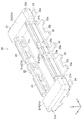
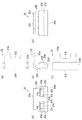
20 ヘッダ
21 ヘッダハウジング
22 ヘッダ側信号用端子
22a 付け根部
22c 凹部
22e 被係止部
23 ヘッダ側電源用端子
23a 付け根部
23c 凹部
23e 被係止部
24 ヘッダ側保持金具
24a 固定端子
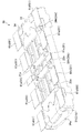
30 ソケット
31 ソケットハウジング
31s 外面
31t 側面
31u 底面
32 ソケット側信号用端子
32a 付け根部
33 ソケット側電源用端子
33a 付け根部
35 片部
36 片部
34 ソケット側保持金具
34d 固定端子
34j 第1の固定端子
34k 第2の固定端子
34e 外壁面
34f 外面
40 第2の回路基板
41 回路パターン
50 半田
60 第1の回路基板
61 回路パターン
70 半田
R1〜R5 接点部
C1、C2 接点
X 長手方向
Y 短手方向(幅方向)
Z 上下方向
Claims (8)
- ソケット側信号用端子およびソケット側電源用端子が配設される略矩形状のソケットハウジングを有するソケットと、ヘッダ側信号用端子およびヘッダ側電源用端子が配設される略矩形状のヘッダハウジングを有するヘッダと、を備え、前記ソケットハウジングと前記ヘッダハウジングとを嵌合させることで、前記ソケット側信号用端子と前記ヘッダ側信号用端子とが接触するとともに、前記ソケット側電源用端子と前記ヘッダ側電源用端子とが接触するコネクタであって、
前記ソケットハウジングには、側板部と、前記側板部から前記ソケットハウジングの長手方向の内側に延設されるとともに、板厚方向が回路基板の表面と交差する方向となる底板部と、を有するソケット側保持金具が配設されており、
前記ソケット側保持金具は、前記回路基板に形成された回路パターンに半田付けされる固定端子を有しており、
前記ソケット側電源用端子は、前記回路基板に形成された回路パターンに半田付けされる付け根部を有しており、
前記固定端子と前記付け根部とが共通の回路パターンに半田付けされており、
前記固定端子は、前記底板部から延設される第1の固定端子と、前記側板部から延設され、当該第1の固定端子とは別に形成される第2の固定端子と、を有しており、
互いに近傍に配置される前記第1の固定端子と前記第2の固定端子とで形成される固定端子の組が2組形成されていることを特徴とするコネクタ。 - 前記ソケット側保持金具と前記ソケット側電源用端子とが隣り合うように配置されていることを特徴とする請求項1に記載のコネクタ。
- 前記ソケット側保持金具の少なくとも一部が前記ソケットハウジングの外面に沿って露出していることを特徴とする請求項1または請求項2に記載のコネクタ。
- 前記ソケット側保持金具は、前記ソケットハウジングの側面および底面のうち少なくともいずれか一方の面に沿って露出していることを特徴とする請求項3に記載のコネクタ。
- 前記ソケット側保持金具がインサート成形によって前記ソケットハウジングに配設されていることを特徴とする請求項1〜4のうちいずれか1項に記載のコネクタ。
- 前記第1の固定端子および前記第2の固定端子が、前記付け根部が半田付けされる回路パターンに半田付けされていることを特徴とする請求項1〜5のうちいずれか1項に記載のコネクタ。
- ソケット側信号用端子およびソケット側電源用端子が配設される略矩形状のソケットハウジングを有するソケットと、ヘッダ側信号用端子およびヘッダ側電源用端子が配設される略矩形状のヘッダハウジングを有するヘッダと、を備え、前記ソケットハウジングと前記ヘッダハウジングとを嵌合させることで、前記ソケット側信号用端子と前記ヘッダ側信号用端子とが接触するとともに、前記ソケット側電源用端子と前記ヘッダ側電源用端子とが接触するコネクタであって、
前記ソケットハウジングには、側板部と、前記側板部から前記ソケットハウジングの長手方向の内側に延設されるとともに、板厚方向が第1の回路基板の表面と交差する方向となる底板部と、を有するソケット側保持金具が配設されており、
前記ソケット側保持金具は、前記第1の回路基板に形成された回路パターンに半田付けされる固定端子を有しており、
前記ソケット側電源用端子は、前記第1の回路基板に形成された回路パターンに半田付けされる付け根部を有しており、
前記固定端子と前記ソケット側電源用端子の付け根部とが、前記第1の回路基板に形成された共通の回路パターンに半田付けされており、
前記ヘッダハウジングには、ヘッダ側保持金具が配設されており、
前記ヘッダ側保持金具は、第2の回路基板に形成された回路パターンに半田付けされる固定端子を有しており、
前記ヘッダ側電源用端子は、前記第2の回路基板に形成された回路パターンに半田付けされる付け根部を有しており、
前記固定端子と前記ヘッダ側電源用端子の付け根部とが、前記第2の回路基板に形成された共通の回路パターンに半田付けされており、
前記ソケット側保持金具の固定端子は、前記底板部から延設される第1の固定端子と、前記側板部から延設され、当該第1の固定端子とは別に形成される第2の固定端子と、を有しており、
互いに近傍に配置される前記第1の固定端子と前記第2の固定端子とで形成される固定端子の組が2組形成されていることを特徴とするコネクタ。 - 請求項1〜7のうちいずれか1項に記載のコネクタに用いられるソケット。
Priority Applications (7)
| Application Number | Priority Date | Filing Date | Title |
|---|---|---|---|
| JP2014161129A JP6473990B2 (ja) | 2014-08-07 | 2014-08-07 | コネクタおよび当該コネクタに用いられるソケット |
| US15/314,576 US9843117B2 (en) | 2014-08-07 | 2015-08-03 | Connector, and header and socket which are used in connector |
| CN201580031833.7A CN106663888B (zh) | 2014-08-07 | 2015-08-03 | 连接器以及在该连接器中使用的插头件及插口件 |
| EP15828990.0A EP3179568B1 (en) | 2014-08-07 | 2015-08-03 | Connector and header and socket used in said connector |
| PCT/JP2015/003896 WO2016021177A1 (ja) | 2014-08-07 | 2015-08-03 | コネクタおよび当該コネクタに用いられるヘッダならびにソケット |
| CN201910466241.8A CN110165446B (zh) | 2014-08-07 | 2015-08-03 | 插口件 |
| US15/808,678 US10305205B2 (en) | 2014-08-07 | 2017-11-09 | Connector, and header and socket which are used in connector |
Applications Claiming Priority (1)
| Application Number | Priority Date | Filing Date | Title |
|---|---|---|---|
| JP2014161129A JP6473990B2 (ja) | 2014-08-07 | 2014-08-07 | コネクタおよび当該コネクタに用いられるソケット |
Related Child Applications (1)
| Application Number | Title | Priority Date | Filing Date |
|---|---|---|---|
| JP2018213132A Division JP6643641B2 (ja) | 2018-11-13 | 2018-11-13 | コネクタ、ソケットおよびソケットと回路基板との接続構造 |
Publications (3)
| Publication Number | Publication Date |
|---|---|
| JP2016039017A JP2016039017A (ja) | 2016-03-22 |
| JP2016039017A5 JP2016039017A5 (ja) | 2017-02-16 |
| JP6473990B2 true JP6473990B2 (ja) | 2019-02-27 |
Family
ID=55263472
Family Applications (1)
| Application Number | Title | Priority Date | Filing Date |
|---|---|---|---|
| JP2014161129A Active JP6473990B2 (ja) | 2014-08-07 | 2014-08-07 | コネクタおよび当該コネクタに用いられるソケット |
Country Status (5)
| Country | Link |
|---|---|
| US (2) | US9843117B2 (ja) |
| EP (1) | EP3179568B1 (ja) |
| JP (1) | JP6473990B2 (ja) |
| CN (2) | CN106663888B (ja) |
| WO (1) | WO2016021177A1 (ja) |
Families Citing this family (8)
| Publication number | Priority date | Publication date | Assignee | Title |
|---|---|---|---|---|
| JP6712799B2 (ja) * | 2016-02-05 | 2020-06-24 | パナソニックIpマネジメント株式会社 | コネクタおよび当該コネクタに用いられるヘッダならびにソケット |
| JP6512210B2 (ja) * | 2016-12-21 | 2019-05-15 | 第一精工株式会社 | コネクタ装置 |
| JP6894320B2 (ja) * | 2017-08-21 | 2021-06-30 | ヒロセ電機株式会社 | 回路基板用電気コネクタ |
| JP1625950S (ja) * | 2018-06-22 | 2019-03-04 | ||
| KR102606247B1 (ko) * | 2018-07-30 | 2023-11-27 | 삼성전자주식회사 | 도전성 핀의 적어도 일부를 지지하기 위한 지지 부분을 포함하는 커넥터 및 이를 포함하는 전자 장치 |
| JP7411882B2 (ja) * | 2019-08-08 | 2024-01-12 | パナソニックIpマネジメント株式会社 | コネクタ |
| JP1656956S (ja) * | 2019-11-11 | 2020-04-06 | ||
| JP1656955S (ja) * | 2019-11-11 | 2020-04-06 |
Family Cites Families (16)
| Publication number | Priority date | Publication date | Assignee | Title |
|---|---|---|---|---|
| US5685729A (en) * | 1995-06-02 | 1997-11-11 | General Motors Corporation | Electrical connector and vent tube assembly with connector position assurance |
| JP3423560B2 (ja) * | 1996-05-29 | 2003-07-07 | ケル株式会社 | コネクタ |
| JP2005019144A (ja) * | 2003-06-25 | 2005-01-20 | Matsushita Electric Works Ltd | コネクタ |
| JP2005294034A (ja) * | 2004-03-31 | 2005-10-20 | Matsushita Electric Works Ltd | コネクタ |
| JP4219308B2 (ja) * | 2004-08-18 | 2009-02-04 | ヒロセ電機株式会社 | ロック機能付き補強金具及びそれを備えたコネクタ |
| JP2008270085A (ja) * | 2007-04-24 | 2008-11-06 | Matsushita Electric Works Ltd | コネクタ |
| JP5623694B2 (ja) * | 2008-05-12 | 2014-11-12 | オムロン株式会社 | コネクタ |
| SG166707A1 (en) * | 2009-06-03 | 2010-12-29 | 3M Innovative Properties Co | Connector |
| JP5807181B2 (ja) * | 2011-02-07 | 2015-11-10 | パナソニックIpマネジメント株式会社 | 保持金具、コネクタ接続体およびコネクタ |
| JP2013101909A (ja) * | 2011-10-14 | 2013-05-23 | Molex Inc | コネクタ |
| CN103050805B (zh) * | 2011-10-14 | 2014-12-10 | 莫列斯公司 | 连接器 |
| JP5638026B2 (ja) * | 2012-05-01 | 2014-12-10 | ヒロセ電機株式会社 | 電気コネクタ組立体 |
| JP6245964B2 (ja) | 2013-12-02 | 2017-12-13 | モレックス エルエルシー | コネクタ |
| JP5887326B2 (ja) * | 2013-12-12 | 2016-03-16 | モレックス エルエルシー | コネクタ |
| KR20150084563A (ko) * | 2014-01-14 | 2015-07-22 | 삼성디스플레이 주식회사 | 커넥터 어셈블리 및 이를 갖는 표시장치 |
| US9420658B2 (en) * | 2014-12-05 | 2016-08-16 | Xenio Corporation | Inrush energy control for a light emitter |
-
2014
- 2014-08-07 JP JP2014161129A patent/JP6473990B2/ja active Active
-
2015
- 2015-08-03 CN CN201580031833.7A patent/CN106663888B/zh active Active
- 2015-08-03 WO PCT/JP2015/003896 patent/WO2016021177A1/ja active Application Filing
- 2015-08-03 EP EP15828990.0A patent/EP3179568B1/en active Active
- 2015-08-03 US US15/314,576 patent/US9843117B2/en active Active
- 2015-08-03 CN CN201910466241.8A patent/CN110165446B/zh active Active
-
2017
- 2017-11-09 US US15/808,678 patent/US10305205B2/en active Active
Also Published As
| Publication number | Publication date |
|---|---|
| CN106663888A (zh) | 2017-05-10 |
| EP3179568A1 (en) | 2017-06-14 |
| CN110165446B (zh) | 2021-07-09 |
| EP3179568B1 (en) | 2020-03-11 |
| US9843117B2 (en) | 2017-12-12 |
| US20180069332A1 (en) | 2018-03-08 |
| WO2016021177A1 (ja) | 2016-02-11 |
| CN110165446A (zh) | 2019-08-23 |
| US10305205B2 (en) | 2019-05-28 |
| CN106663888B (zh) | 2019-06-28 |
| JP2016039017A (ja) | 2016-03-22 |
| EP3179568A4 (en) | 2017-07-26 |
| US20170194727A1 (en) | 2017-07-06 |
Similar Documents
| Publication | Publication Date | Title |
|---|---|---|
| JP6473990B2 (ja) | コネクタおよび当該コネクタに用いられるソケット | |
| JP6388152B2 (ja) | コネクタおよび当該コネクタに用いられるヘッダならびにソケット | |
| JP6712794B2 (ja) | コネクタおよび当該コネクタに用いられるヘッダならびにソケット | |
| WO2017134719A1 (ja) | コネクタおよび当該コネクタに用いられるヘッダならびにソケット | |
| TWI445252B (zh) | 卡緣連接器 | |
| WO2017187993A1 (ja) | コネクタ、ヘッダおよびソケット | |
| JP4805422B1 (ja) | コネクタ | |
| JP6681577B2 (ja) | コネクタおよび当該コネクタに用いられるヘッダならびにソケット | |
| JP2019021651A (ja) | コネクタおよびソケット | |
| WO2017187992A1 (ja) | 保持金具、コネクタ接続体およびコネクタ | |
| JP7300632B2 (ja) | コネクタ接続体およびコネクタ | |
| JP7033737B2 (ja) | コネクタ接続体およびコネクタ | |
| US7749000B1 (en) | Electrical connector | |
| US7476109B2 (en) | Electrical connector assembled with a bondable element |
Legal Events
| Date | Code | Title | Description |
|---|---|---|---|
| A521 | Request for written amendment filed |
Free format text: JAPANESE INTERMEDIATE CODE: A523 Effective date: 20170111 |
|
| A621 | Written request for application examination |
Free format text: JAPANESE INTERMEDIATE CODE: A621 Effective date: 20170605 |
|
| A131 | Notification of reasons for refusal |
Free format text: JAPANESE INTERMEDIATE CODE: A131 Effective date: 20180227 |
|
| A521 | Request for written amendment filed |
Free format text: JAPANESE INTERMEDIATE CODE: A523 Effective date: 20180501 |
|
| A02 | Decision of refusal |
Free format text: JAPANESE INTERMEDIATE CODE: A02 Effective date: 20180814 |
|
| A521 | Request for written amendment filed |
Free format text: JAPANESE INTERMEDIATE CODE: A523 Effective date: 20181113 |
|
| A911 | Transfer to examiner for re-examination before appeal (zenchi) |
Free format text: JAPANESE INTERMEDIATE CODE: A911 Effective date: 20181120 |
|
| TRDD | Decision of grant or rejection written | ||
| A01 | Written decision to grant a patent or to grant a registration (utility model) |
Free format text: JAPANESE INTERMEDIATE CODE: A01 Effective date: 20190115 |
|
| A61 | First payment of annual fees (during grant procedure) |
Free format text: JAPANESE INTERMEDIATE CODE: A61 Effective date: 20190118 |
|
| R151 | Written notification of patent or utility model registration |
Ref document number: 6473990 Country of ref document: JP Free format text: JAPANESE INTERMEDIATE CODE: R151 |