JP6449286B2 - Contactor for electric shock protection and portable electronic device having the same - Google Patents
Contactor for electric shock protection and portable electronic device having the same Download PDFInfo
- Publication number
- JP6449286B2 JP6449286B2 JP2016534239A JP2016534239A JP6449286B2 JP 6449286 B2 JP6449286 B2 JP 6449286B2 JP 2016534239 A JP2016534239 A JP 2016534239A JP 2016534239 A JP2016534239 A JP 2016534239A JP 6449286 B2 JP6449286 B2 JP 6449286B2
- Authority
- JP
- Japan
- Prior art keywords
- electric shock
- shock protection
- contactor
- conductive
- conductor
- Prior art date
- Legal status (The legal status is an assumption and is not a legal conclusion. Google has not performed a legal analysis and makes no representation as to the accuracy of the status listed.)
- Active
Links
- 239000010410 layer Substances 0.000 claims description 115
- 239000004020 conductor Substances 0.000 claims description 87
- 239000000463 material Substances 0.000 claims description 57
- 239000003990 capacitor Substances 0.000 claims description 52
- 230000005611 electricity Effects 0.000 claims description 36
- 230000003068 static effect Effects 0.000 claims description 36
- 238000004891 communication Methods 0.000 claims description 33
- 230000015556 catabolic process Effects 0.000 claims description 29
- 229920002379 silicone rubber Polymers 0.000 claims description 29
- 239000002184 metal Substances 0.000 claims description 17
- 229910052751 metal Inorganic materials 0.000 claims description 17
- 239000012790 adhesive layer Substances 0.000 claims description 10
- 239000004945 silicone rubber Substances 0.000 claims description 8
- 230000008878 coupling Effects 0.000 claims description 4
- 238000010168 coupling process Methods 0.000 claims description 4
- 238000005859 coupling reaction Methods 0.000 claims description 4
- 244000043261 Hevea brasiliensis Species 0.000 claims description 3
- 229920003052 natural elastomer Polymers 0.000 claims description 3
- 229920001194 natural rubber Polymers 0.000 claims description 3
- 229920000642 polymer Polymers 0.000 claims description 3
- 229920003051 synthetic elastomer Polymers 0.000 claims description 3
- 239000005061 synthetic rubber Substances 0.000 claims description 3
- HBMJWWWQQXIZIP-UHFFFAOYSA-N silicon carbide Chemical compound [Si+]#[C-] HBMJWWWQQXIZIP-UHFFFAOYSA-N 0.000 description 8
- 229910010271 silicon carbide Inorganic materials 0.000 description 8
- 229910010293 ceramic material Inorganic materials 0.000 description 4
- 230000002829 reductive effect Effects 0.000 description 4
- 230000035945 sensitivity Effects 0.000 description 4
- 239000002131 composite material Substances 0.000 description 3
- 238000010586 diagram Methods 0.000 description 3
- 239000002245 particle Substances 0.000 description 3
- 239000004065 semiconductor Substances 0.000 description 3
- 238000000926 separation method Methods 0.000 description 3
- 238000004088 simulation Methods 0.000 description 3
- 229910006404 SnO 2 Inorganic materials 0.000 description 2
- 230000002238 attenuated effect Effects 0.000 description 2
- 230000005540 biological transmission Effects 0.000 description 2
- 230000000903 blocking effect Effects 0.000 description 2
- 150000001875 compounds Chemical class 0.000 description 2
- 238000009413 insulation Methods 0.000 description 2
- 239000012212 insulator Substances 0.000 description 2
- 238000010030 laminating Methods 0.000 description 2
- 229910044991 metal oxide Inorganic materials 0.000 description 2
- -1 metal oxide compound Chemical class 0.000 description 2
- 239000002923 metal particle Substances 0.000 description 2
- 229910052759 nickel Inorganic materials 0.000 description 2
- 239000000126 substance Substances 0.000 description 2
- 229910017493 Nd 2 O 3 Inorganic materials 0.000 description 1
- 229910052777 Praseodymium Inorganic materials 0.000 description 1
- XUIMIQQOPSSXEZ-UHFFFAOYSA-N Silicon Chemical compound [Si] XUIMIQQOPSSXEZ-UHFFFAOYSA-N 0.000 description 1
- 229910002367 SrTiO Inorganic materials 0.000 description 1
- 230000002411 adverse Effects 0.000 description 1
- 238000005452 bending Methods 0.000 description 1
- 229910052797 bismuth Inorganic materials 0.000 description 1
- 230000001413 cellular effect Effects 0.000 description 1
- 238000006243 chemical reaction Methods 0.000 description 1
- 230000000295 complement effect Effects 0.000 description 1
- 229910052802 copper Inorganic materials 0.000 description 1
- 230000007547 defect Effects 0.000 description 1
- 230000002542 deteriorative effect Effects 0.000 description 1
- 230000000694 effects Effects 0.000 description 1
- 238000010292 electrical insulation Methods 0.000 description 1
- 238000005516 engineering process Methods 0.000 description 1
- 239000010419 fine particle Substances 0.000 description 1
- 229910052737 gold Inorganic materials 0.000 description 1
- 238000004519 manufacturing process Methods 0.000 description 1
- 238000000034 method Methods 0.000 description 1
- 239000012811 non-conductive material Substances 0.000 description 1
- 230000001590 oxidative effect Effects 0.000 description 1
- 229910052763 palladium Inorganic materials 0.000 description 1
- 229910052697 platinum Inorganic materials 0.000 description 1
- 239000000047 product Substances 0.000 description 1
- 230000000644 propagated effect Effects 0.000 description 1
- 230000001681 protective effect Effects 0.000 description 1
- 229910052710 silicon Inorganic materials 0.000 description 1
- 239000010703 silicon Substances 0.000 description 1
- 229910052709 silver Inorganic materials 0.000 description 1
- 239000013589 supplement Substances 0.000 description 1
- 229910052718 tin Inorganic materials 0.000 description 1
Images


Classifications
-
- H—ELECTRICITY
- H01—ELECTRIC ELEMENTS
- H01R—ELECTRICALLY-CONDUCTIVE CONNECTIONS; STRUCTURAL ASSOCIATIONS OF A PLURALITY OF MUTUALLY-INSULATED ELECTRICAL CONNECTING ELEMENTS; COUPLING DEVICES; CURRENT COLLECTORS
- H01R13/00—Details of coupling devices of the kinds covered by groups H01R12/70 or H01R24/00 - H01R33/00
- H01R13/02—Contact members
- H01R13/22—Contacts for co-operating by abutting
- H01R13/24—Contacts for co-operating by abutting resilient; resiliently-mounted
- H01R13/2407—Contacts for co-operating by abutting resilient; resiliently-mounted characterized by the resilient means
-
- H—ELECTRICITY
- H05—ELECTRIC TECHNIQUES NOT OTHERWISE PROVIDED FOR
- H05K—PRINTED CIRCUITS; CASINGS OR CONSTRUCTIONAL DETAILS OF ELECTRIC APPARATUS; MANUFACTURE OF ASSEMBLAGES OF ELECTRICAL COMPONENTS
- H05K9/00—Screening of apparatus or components against electric or magnetic fields
- H05K9/0067—Devices for protecting against damage from electrostatic discharge
-
- H—ELECTRICITY
- H01—ELECTRIC ELEMENTS
- H01C—RESISTORS
- H01C7/00—Non-adjustable resistors formed as one or more layers or coatings; Non-adjustable resistors made from powdered conducting material or powdered semi-conducting material with or without insulating material
- H01C7/10—Non-adjustable resistors formed as one or more layers or coatings; Non-adjustable resistors made from powdered conducting material or powdered semi-conducting material with or without insulating material voltage responsive, i.e. varistors
- H01C7/12—Overvoltage protection resistors
-
- H—ELECTRICITY
- H01—ELECTRIC ELEMENTS
- H01R—ELECTRICALLY-CONDUCTIVE CONNECTIONS; STRUCTURAL ASSOCIATIONS OF A PLURALITY OF MUTUALLY-INSULATED ELECTRICAL CONNECTING ELEMENTS; COUPLING DEVICES; CURRENT COLLECTORS
- H01R13/00—Details of coupling devices of the kinds covered by groups H01R12/70 or H01R24/00 - H01R33/00
- H01R13/02—Contact members
- H01R13/22—Contacts for co-operating by abutting
- H01R13/24—Contacts for co-operating by abutting resilient; resiliently-mounted
- H01R13/2407—Contacts for co-operating by abutting resilient; resiliently-mounted characterized by the resilient means
- H01R13/2414—Contacts for co-operating by abutting resilient; resiliently-mounted characterized by the resilient means conductive elastomers
-
- H—ELECTRICITY
- H01—ELECTRIC ELEMENTS
- H01R—ELECTRICALLY-CONDUCTIVE CONNECTIONS; STRUCTURAL ASSOCIATIONS OF A PLURALITY OF MUTUALLY-INSULATED ELECTRICAL CONNECTING ELEMENTS; COUPLING DEVICES; CURRENT COLLECTORS
- H01R13/00—Details of coupling devices of the kinds covered by groups H01R12/70 or H01R24/00 - H01R33/00
- H01R13/02—Contact members
- H01R13/22—Contacts for co-operating by abutting
- H01R13/24—Contacts for co-operating by abutting resilient; resiliently-mounted
- H01R13/2442—Contacts for co-operating by abutting resilient; resiliently-mounted with a single cantilevered beam
-
- H—ELECTRICITY
- H01—ELECTRIC ELEMENTS
- H01R—ELECTRICALLY-CONDUCTIVE CONNECTIONS; STRUCTURAL ASSOCIATIONS OF A PLURALITY OF MUTUALLY-INSULATED ELECTRICAL CONNECTING ELEMENTS; COUPLING DEVICES; CURRENT COLLECTORS
- H01R13/00—Details of coupling devices of the kinds covered by groups H01R12/70 or H01R24/00 - H01R33/00
- H01R13/66—Structural association with built-in electrical component
- H01R13/665—Structural association with built-in electrical component with built-in electronic circuit
- H01R13/6666—Structural association with built-in electrical component with built-in electronic circuit with built-in overvoltage protection
Description
本発明は、感電保護用コンタクター及びそれを備えた携帯用電子装置に関する。さらに詳しくは、電源によるリーク電流から使用者を保護することができる感電保護用コンタクター及びそれを備えた携帯用電子装置に関するものである。 The present invention relates to an electric shock protection contactor and a portable electronic device having the same. More particularly, the present invention relates to an electric shock protection contactor capable of protecting a user from a leakage current caused by a power supply and a portable electronic device including the same.
近頃の携帯用電子装置は、小型化及び多機能化に伴い、内部に様々な部品素子が密集配置される。従って、外部からの衝撃を緩和させると同時に、携帯用電子装置内部に浸透するか、携帯用電子装置から漏洩される電磁波を低減させるために外装ハウジングと携帯用電子装置の内蔵回路基板と間に導電性ガスケットが使用されている。 In recent portable electronic devices, various component elements are densely arranged inside as the size and the number of functions are increased. Accordingly, in order to reduce the electromagnetic wave that penetrates into the portable electronic device or leaks from the portable electronic device while reducing the impact from the outside, between the exterior housing and the built-in circuit board of the portable electronic device. A conductive gasket is used.
また、携帯用電子装置は、多機能化に伴い、機能別に複数のアンテナを備え、その中の少なくとも一部は、内蔵型アンテナであり、携帯用電子装置の外装ハウジングに配置される。従って、外装ハウジングに配置されたアンテナと携帯用電子装置の内蔵回路基板と間に電気的接触のための導電性コンタクターが使用されている。 In addition, with the increase in functionality of portable electronic devices, a plurality of antennas are provided for each function, and at least some of them are built-in antennas, which are arranged in an exterior housing of the portable electronic device. Therefore, a conductive contactor for electrical contact is used between the antenna disposed in the exterior housing and the built-in circuit board of the portable electronic device.
また、携帯用電子装置は、審美性と堅固さを向上させるためにメタル材質のハウジングの採択が増加しつつある。 Also, the adoption of metal housings is increasing for portable electronic devices in order to improve aesthetics and rigidity.
結果的に、導電性ガスケットまたは導電性コンタクターにより、外装ハウジングと内蔵回路基板と間に電気的経路が形成されており、特に、メタルハウジングと回路基板がループを形成することによって、外部の露出面積が大きなメタルハウジングのような伝導体を通して瞬間的に高い電圧を有する静電気が流入される場合、導電性ガスケットまたは導電性コンタクターを通して静電気が内蔵回路基板に流入され、ICなどの回路が破損されることがある。 As a result, an electrical path is formed between the outer housing and the built-in circuit board by the conductive gasket or the conductive contactor. In particular, the metal housing and the circuit board form a loop, so that an external exposed area is formed. When static electricity with a high voltage is instantaneously flowed through a conductor such as a large metal housing, static electricity flows into the built-in circuit board through a conductive gasket or conductive contactor, and the circuit such as an IC is damaged. There is.
一方、このような携帯用電子装置は、通常的に充電器を使用して電池を充電する。このような充電器は、外部のAC電源をDC電源に整流した後、再び、トランスフォーマーを介して携帯用電子装置に適した低いDC電源に変換する。ここで、トランスフォーマーの電気的絶縁性を強化させるために、トランスフォーマー両端にキャパシタで構成されたY−CAPを備える。 On the other hand, such portable electronic devices typically use a charger to charge the battery. Such a charger rectifies an external AC power source into a DC power source, and then converts it again into a low DC power source suitable for a portable electronic device via a transformer. Here, in order to reinforce the electrical insulation of the transformer, Y-CAP composed of capacitors is provided at both ends of the transformer.
しかし、非正規商品充電器などのように、Y−CAPが正規特性を有しない場合には、Y−CAPによりDC電源が十分に遮断できない可能性もあり、さらに、AC電源によりリーク電流が生ずることがあり、このようなリーク電流は回路の接地部に沿って伝播される。 However, when the Y-CAP does not have normal characteristics, such as a non-regular product charger, the DC power supply may not be sufficiently cut off by the Y-CAP, and further, a leakage current is generated by the AC power supply. In some cases, such leakage current is propagated along the circuit ground.
このようなリーク電流は、携帯用電子装置の外装ケースのように人体が接触可能な伝導体にも伝達されることがあるため、結果的に使用者に、ピリピリとした感じの不快感を与えており、激しい場合、使用者に弊害を与える感電事故を招く問題があった。 Such a leakage current may be transmitted to a conductor that can be contacted by a human body, such as an exterior case of a portable electronic device, and as a result, the user feels uncomfortable. In severe cases, there has been a problem of causing an electric shock that is harmful to the user.
従って、このようなリーク電流から使用者を保護するための保護用素子がメタルハウジングと回路基板を連結する導電性ガスケットまたは導電性コンタクターに備えられる必要がある。 Accordingly, it is necessary to provide a protective element for protecting the user from such a leakage current in a conductive gasket or a conductive contactor that connects the metal housing and the circuit board.
さらに、メタルハウジングがアンテナとして使われる場合、導電性ガスケットまたは導電性コンタクターは、キャパシタンスが低ければ信号の減殺が生じ、RF信号の伝達が円滑に進まないので、高いキャパシタンスを具現する必要がある。 In addition, when a metal housing is used as an antenna, a conductive gasket or a conductive contactor needs to realize a high capacitance because signal attenuation occurs when the capacitance is low, and transmission of the RF signal does not proceed smoothly.
このように、メタルケースのような伝導体の使用により、単純な電気的な接触だけでなく、使用者または携帯用電子装置内の回路を保護するための様々な機能を備えたコンタクターが求められている。 Thus, the use of a conductor such as a metal case requires not only a simple electrical contact but also a contactor with various functions for protecting the circuit in the user or portable electronic device. ing.
しかし、かかる様々な機能を具現するためには、追加的な部品素子が必要とされており、従って、携帯用電子装置の回路基板に追加的な空間が確保されなければならないため、小型化に悪影響を及ぼす問題があった。 However, in order to realize such various functions, an additional component element is required, and therefore, an additional space must be secured on the circuit board of the portable electronic device. There was a problem that had an adverse effect.
本発明は、前述のような点を勘案して案出されたものであり、外部電源によるリーク電流から使用者を保護することができる感電保護用コンタクター及びそれを備えた携帯用電子装置を提供することに目的がある。 The present invention has been devised in view of the above-described points, and provides an electric shock protection contactor capable of protecting a user from a leakage current caused by an external power source and a portable electronic device including the same. There is a purpose to do.
また、本発明は、静電気によるリーク電流から内部回路を保護することができる感電保護用コンタクター及びそれを備えた携帯用電子装置を提供することに目的がある。 Another object of the present invention is to provide a contactor for electric shock protection capable of protecting an internal circuit from a leakage current due to static electricity, and a portable electronic device including the same.
また、本発明は、通信信号の減殺を最小化して伝達することができる感電保護用コンタクター及びそれを備えた携帯用電子装置を提供することに目的がある。 Another object of the present invention is to provide an electric shock protection contactor capable of minimizing communication signal loss and transmitting it, and a portable electronic device having the same.
前述した課題を解決するために、本発明は、電子装置の伝導体に電気的に接触する導電性連結部と、前記導電性連結部に直列連結され、前記電子装置の回路基板の接地から流入される外部電源のリーク電流を遮断する感電保護素子と、
を含む感電保護用コンタクターを提供する。
In order to solve the above-described problem, the present invention provides a conductive connection portion that is in electrical contact with a conductor of an electronic device, and is connected in series to the conductive connection portion and flows from a ground of a circuit board of the electronic device. An electric shock protection element that cuts off the leakage current of the external power supply,
The contactor for electric shock protection including is provided.
また、前記感電保護素子は、前記伝導体から流入される通信信号を通過させる。 Further, the electric shock protection element allows a communication signal flowing from the conductor to pass therethrough.
また、前記感電保護素子は、前記伝導体から静電気流入時、絶縁破壊されずに前記静電気を通過させる。 The electric shock protection element allows the static electricity to pass through without being broken down when static electricity flows from the conductor.
また、前記感電保護素子は、上側に溝部を備え、
前記導電性連結部は、前記溝部に少なくとも一部が挿入される。
The electric shock protection element includes a groove on the upper side,
At least a part of the conductive connecting portion is inserted into the groove portion.
また、前記感電保護素子は、下記数式(1)を満たす降伏電圧Vbrを有する: The electric shock protection device has a breakdown voltage Vbr that satisfies the following mathematical formula (1):
![]()
![]()
(式中、Vinは、前記電子装置の外部電源の定格電圧である。)
また、前記感電保護素子は、感電保護部及び少なくとも一つのキャパシタ層を含み、前記感電保護部は、下記式を満たす降伏電圧Vbrを有する:
(Where Vin is the rated voltage of the external power supply of the electronic device.)
The electric shock protection device includes an electric shock protection unit and at least one capacitor layer, and the electric shock protection unit has a breakdown voltage Vbr that satisfies the following formula:
![]()
![]()
(式中、Vinは、前記電子装置の外部電源の定格電圧であり、
Vcpは、前記キャパシタ層の絶縁破壊電圧である。)
(Where Vin is the rated voltage of the external power supply of the electronic device,
Vcp is a breakdown voltage of the capacitor layer. )
また、前記導電性連結部は、導電性ガスケット、シリコンゴムパッド、弾性力を有するクリップ状の伝導体である。 The conductive connecting portion is a conductive gasket, a silicon rubber pad, or a clip-like conductor having elasticity.
また、前記導電性ガスケットは、導電性ペーストが熱圧着により作製されたポリマー胴体、天然ゴム、スポンジ、合成ゴム、耐熱性シリコンゴム及びチューブの少なくともいずれか一つを含む。 The conductive gasket includes at least one of a polymer body, natural rubber, sponge, synthetic rubber, heat-resistant silicon rubber, and a tube in which a conductive paste is manufactured by thermocompression bonding.
また、前記シリコンゴムパッドは、シリコンゴムからなる胴体と、前記胴体内部に垂直形成される導電性ワイヤーと、を含む。 The silicon rubber pad includes a body made of silicon rubber and a conductive wire formed vertically in the body.
また、前記シリコンゴムパッドは、シリコンゴムからなる胴体と、前記胴体内部に斜線で形成された導電性ワイヤーと、を含む。 In addition, the silicon rubber pad includes a body made of silicon rubber and a conductive wire formed by oblique lines inside the body.
また、前記シリコンゴムパッドは、シリコンゴムからなる胴体と、前記胴体内部に水平に交差積層された複数の伝導層と、前記胴体の上側に曲線突起状に形成された複数の接触部と、を含む。 The silicon rubber pad includes a body made of silicon rubber, a plurality of conductive layers horizontally intersecting and laminated inside the body, and a plurality of contact portions formed in a curved protrusion shape on the upper side of the body. .
また、前記クリップ状の伝導体は、湾曲部状を有し、前記接触する伝導体と接触する接触部と、前記接触部から延長形成され、弾性力を有する延長部と、前記感電保護素子と電気的に連結される端子部と、を含む。 In addition, the clip-like conductor has a curved portion shape, a contact portion that contacts the contacting conductor, an extension portion that is formed extending from the contact portion and has an elastic force, and the electric shock protection element A terminal portion that is electrically connected.
また、前記感電保護素子は、前記溝部の底面に外部電極が備えられ、前記導電性連結部は、導電性接着層を介して前記外部電極上に積層される。 The electric shock protection element includes an external electrode on a bottom surface of the groove, and the conductive connection portion is stacked on the external electrode through a conductive adhesive layer.
また、前記感電保護素子は、複数のシート層が積層された焼体と、前記焼体の内部に、一定の間隔で離隔され形成された少なくとも一対の内部電極と、前記内部電極間に形成された空隙と、を含む。 In addition, the electric shock protection element is formed between a sintered body in which a plurality of sheet layers are laminated, at least a pair of internal electrodes formed at a predetermined interval inside the sintered body, and the internal electrodes. Voids.
また、前記一対の内部電極は、同一平面上で配置される。 Further, the pair of internal electrodes are arranged on the same plane.
また、前記空隙は、内壁に高さ方向に沿って一定の厚さで塗布される放電物質層が備えられる。 In addition, the gap includes a discharge material layer applied to the inner wall with a certain thickness along the height direction.
また、前記感電保護素子は、第1バリスタ物質層と第2バリスタ物質層とが交互に積層された少なくとも2個のバリスタ物質層と、前記第1バリスタ物質層上に一定の間隔Lで離隔された複数の第1内部電極と、前記第2バリスタ物質層上に一定の間隔Lで離隔された複数の第2内部電極と、含む。 The electric shock protection device is separated from the first varistor material layer by at least two varistor material layers in which the first varistor material layers and the second varistor material layers are alternately stacked. A plurality of first internal electrodes, and a plurality of second internal electrodes spaced apart from each other by a predetermined distance L on the second varistor material layer.
また、前記降伏電圧Vbrは、最も隣接した第1内部電極と第2内部電極間とにそれぞれ形成される降伏電圧の和である。 The breakdown voltage Vbr is the sum of breakdown voltages formed between the first and second internal electrodes that are closest to each other.
また、前記第1内部電極及び前記第2内部電極のそれぞれは、少なくとも一部が重なるか、互いに重ならないように配置される。 In addition, each of the first internal electrode and the second internal electrode is arranged so that at least a part thereof overlaps or does not overlap each other.
また、前記第1内部電極または前記第2内部電極の離隔間隔Lは、前記第1内部電極と前記第2内部電極と間の最短距離d1と、隣接する他の第2内部電極間の最短距離d2の和より大である。 The separation interval L of the first internal electrode or the second internal electrode is the shortest distance d1 between the first internal electrode and the second internal electrode and the shortest distance between adjacent second internal electrodes. It is larger than the sum of d2.
また、前記キャパシタ層は、前記感電保護部と電気的に並列接続される。 The capacitor layer is electrically connected in parallel with the electric shock protection unit.
また、前記キャパシタ層と前記感電保護部と間の間隔は、前記感電保護部の一対の内部電極間の間隔より大である。 In addition, a distance between the capacitor layer and the electric shock protection unit is larger than a distance between the pair of internal electrodes of the electric shock protection unit.
また、前記感電保護素子は、複数のシート層が積層された焼体と、前記焼体の内部に一定の間隔で離隔され形成された少なくとも一対の内部電極と前記内部電極間に形成された空隙とを含む感電保護部と、前記通信信号を通過させる少なくとも一つの積層キャパシタ層と、を含む。 The electric shock protection element includes a fired body in which a plurality of sheet layers are laminated, at least a pair of internal electrodes formed at a predetermined interval inside the fired body, and a gap formed between the internal electrodes. And an at least one multilayer capacitor layer that allows the communication signal to pass therethrough.
また、前記感電保護素子は、第1バリスタ物質層と第2バリスタ物質層とが交互に積層された少なくとも2個のバリスタ物質層と、前記第1バリスタ物質層上に一定の間隔Lで離隔された複数の第1内部電極と、前記第2バリスタ物質層上に一定の間隔Lで離隔された複数の第2内部電極とを含む感電保護部と、前記通信信号を通過させる少なくとも一つの積層キャパシタ層と、を含む。 The electric shock protection device is separated from the first varistor material layer by at least two varistor material layers in which the first varistor material layers and the second varistor material layers are alternately stacked. A plurality of first internal electrodes; a plurality of second internal electrodes spaced apart from each other by a predetermined distance L on the second varistor material layer; and at least one multilayer capacitor that allows the communication signal to pass therethrough. And a layer.
一方、本発明は、人体接触可能な伝導体と、複数個の手動素子及び能動素子が設けられる回路基板と、一端は前記回路基板と電気的に連結され、他端は前記伝導体と電気的に直列連結される感電保護用コンタクターと、を含み、前記感電保護用コンタクターは、前記伝導体に電気的に接触する導電性連結部と、
前記導電性連結部に直列連結され、前記回路基板の接地から流入される外部電源のリーク電流を遮断する感電保護素子と、を含む携帯用電子装置を提供する。
On the other hand, the present invention provides a human body-contactable conductor, a circuit board provided with a plurality of manual elements and active elements, one end electrically connected to the circuit board, and the other end electrically connected to the conductor. An electric shock protection contactor connected in series with the electric shock protection contactor, and the electric shock protection contactor is in electrical contact with the conductor;
There is provided a portable electronic device including an electric shock protection element connected in series to the conductive connection portion and blocking a leakage current of an external power source flowing from the ground of the circuit board.
また、前記伝導体は、前記電子装置と外部機器との通信のためのアンテナ、メタルケース、及び導電性装身具の少なくとも一つを含む。 The conductor includes at least one of an antenna, a metal case, and a conductive accessory for communication between the electronic device and an external device.
本発明の一実施例に係る感電保護用コンタクター及びそれを備えた携帯用電子装置は、メタルケースのような伝導体が外部に露出される携帯用電子装置において、伝導体と回路基板とを連結するコンタクターに感電保護素子を備えることによって、外部電源によるリーク電流から使用者を保護することができる長所がある。 An electric shock protection contactor according to an embodiment of the present invention and a portable electronic device including the contactor connect a conductor and a circuit board in a portable electronic device in which a conductor such as a metal case is exposed to the outside. By providing the contactor with an electric shock protection element, there is an advantage that a user can be protected from a leakage current caused by an external power source.
本発明は、静電気から内部回路を保護することができる長所がある。 The present invention has an advantage that an internal circuit can be protected from static electricity.
本発明は、感電保護用コンタクターの感電保護素子にキャパシタ層の付加することによって、高いキャパシタンスを具現し、通信信号の減殺を最小化して伝達することができる長所がある。 The present invention has an advantage that by adding a capacitor layer to the electric shock protection element of the electric shock protection contactor, a high capacitance can be realized and communication signals can be minimized and transmitted.
また、本発明は感電保護素子とコンタクターとを一体的に備えることによって、当該機能具現のための別途の素子とそれによる素子の追加的な空間が必要とされなく、携帯用電子装置の小型化に適する長所がある。 In addition, since the present invention integrally includes an electric shock protection element and a contactor, a separate element for realizing the function and an additional space for the element are not required, and the portable electronic device can be downsized. There are advantages to suit.
以下、添付した図面を参照して、本発明の実施例について、本発明が属する技術分野における通常の知識を有した者が容易に実施できるように詳細に説明する。本発明は、種々の異なる形態で具現されることができ、ここで説明する実施例に限定されない。図において本発明を明確に説明するために説明と関係のない部分は省略しており、明細書全体を通して同一または類似の構成要素については同じ参照符号を付する。 Hereinafter, embodiments of the present invention will be described in detail with reference to the accompanying drawings so that those skilled in the art to which the present invention pertains can be easily implemented. The present invention may be embodied in various different forms and is not limited to the embodiments described herein. In the drawings, parts not related to the description are omitted to clearly describe the present invention, and the same reference numerals are given to the same or similar components throughout the specification.
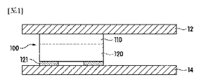
本発明の一実施例に係る感電保護用コンタクター100は、導電性連結部110及び感電保護素子120を含む。
An electric
このような感電保護用コンタクター100は、図1及び図2に示されるように、携帯用電子装置において、外装メタルケースのような伝導体12と回路基板14と間を電気的に連結するためのものである。
As shown in FIGS. 1 and 2, such an electric
ここで、前記携帯用電子装置は、携帯が可能であり、運搬が容易な携帯用電子機器の形態である。一例として、前記携帯用電子装置は、スマートフォン、セルラーフォンなどのような携帯端末機であり、スマートウォッチ、デジタルカメラ、DMB、電子ブック、ネットブック、タブレットPC、携帯用コンピュータなどである。このような電子装置は、外部機器との通信のためのアンテナ構造を含む任意の適切な電子コンポーネントが設けられる。さらに、Wi−Fi及びブルートゥースのような近距離ネットワーク通信を使用する機器である。 Here, the portable electronic device is in the form of a portable electronic device that is portable and easy to carry. As an example, the portable electronic device is a portable terminal such as a smartphone or a cellular phone, and is a smart watch, a digital camera, a DMB, an electronic book, a netbook, a tablet PC, a portable computer, or the like. Such electronic devices are provided with any suitable electronic component including an antenna structure for communication with external equipment. Furthermore, it is a device that uses short-range network communication such as Wi-Fi and Bluetooth.
前記感電保護用コンタクター100は、伝導体12を携帯用電子装置に結合するための加圧力により押圧され、伝導体12を携帯用電子装置から離脱させる場合、元来の状態に復元できるように弾性力を有する。
The electric
ここで、前記伝導体12は、携帯用電子装置の側部を部分的に囲むか、全体的に囲むよう備えられてもよく、前記携帯用電子装置と外部機器との通信のためのアンテナであってもよい。
Here, the
前記導電性連結部110は、携帯用電子装置の伝導体12に電気的に接触して弾性力を有する。このような導電性連結部110は、図1に図示されるような導電性ガスケット、シリコンゴムパッド、及び図2に図示されるような弾性力を有するクリップ状の伝導体である。
The conductive connecting
ここで、前記導電性連結部110が、導電性ガスケットまたはシリコンゴムパッドのように、伝導体12に面接触する場合、導電性連結部110は、弾性力を有する導電性物質で一体的に形成される。このとき、導電性連結部110は伝導体12の加圧力により回路基板14側に収縮し、伝導体12に携帯用電子装置から分離される場合、その弾性力により元来の状態に復元される。
Here, when the conductive connecting
また、前記導電性連結部が弾性力を有するクリップ状の伝導体211、212、213のように、伝導体12に接触する場合、導電性連結部110は、図2に示されるように、接触部211が回路基板14により加圧されることによって、弾性力を有する延長部212が回路基板14側に押圧され、伝導体12が携帯用電子装置から分離される場合、延長部212の弾性力により元来の状態に、即ち、回路基板14の取り付け部位の上側に復元される。
In addition, when the conductive connecting portion contacts the
前記感電保護素子120は、導電性連結部110に電気的に直列連結され、例えば、導電性連結部110の下側に配置される。このとき、前記感電保護素子は、その上面に外部電極が配置される。
The electric
一方、前記感電保護素子120は、上側に溝部を備え、前記溝部の底面に外部電極が備えられ、前記導電性連結部110は、導電性接着層を介して前記外部電極上に積層される。
Meanwhile, the electric
このとき、感電保護素子120は、サプレッサーまたはバリスタである。
At this time, the electric
このような感電保護素子120は、外部電源のリーク電流を遮断できるように下記数式(1)を満たす降伏電圧Vbrを有する:
The electric
![]()
![]()
(式中、Vinは、前記電子装置の外部電源の定格電圧である。)
このとき、前記定格電圧は、国家別標準定格電圧であり、例えば、240V、220V、120V、110V、及び100Vのいずれか一つである。
(Where Vin is the rated voltage of the external power supply of the electronic device.)
At this time, the rated voltage is a national standard rated voltage, for example, one of 240V, 220V, 120V, 110V, and 100V.
一方、前記伝導体12がアンテナ機能を有する場合、前記感電保護素子120は、キャパシタ層を備えたサプレッサーまたはバリスタである。
On the other hand, when the
このような感電保護素子120は、感電保護部及び少なくとも一つのキャパシタ層を含み、外部電源のリーク電流を遮断し、前記伝導体120から流入される通信信号を通過させるように下記式(1)を満たす感電保護部の降伏電圧Vbrを有する:
The electric
![]()
![]()
(式中、Vinは前記電子装置の外部電源の定格電圧である。)
このとき、感電保護素子120が、後端の回路部を保護するために静電気を通過させる機能を有する場合、感電保護部の降伏電圧Vbrは、下記数式(3)の条件を満たす:
(Where Vin is the rated voltage of the external power supply of the electronic device.)
At this time, when the electric
![]()
![]()
(式中、Vcpは、前記キャパシタ層の絶縁破壊電圧である。)
このような感電保護素子120は、図3〜図5に示されるように、外部電源によるリーク電流、伝導体12から流入される静電気及び通信信号に応じて異なる機能を有する。
(Wherein, Vcp is the breakdown voltage of the capacitor layer.)
As shown in FIGS. 3 to 5, the electric
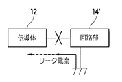
即ち、図3に示されるように、回路基板14の実装された回路部14'、例えば、接地を介して外部電源のリーク電流が伝導体12で流入される場合、感電保護素子120は、その降伏電圧(またはトリガー電圧)Vbrがリーク電流による過電圧に比べて大きいため、オープン状態で維持される。即ち、感電保護素子120の降伏電圧Vbrが携帯用電子装置の外部電源の定格電圧より大きいため、電気的に導通されなく、オープン状態を維持し、メタルケースなどのような人体接着可能な伝導体12にリーク電流が伝達されることを遮断することができる。
That is, as shown in FIG. 3, when the leakage current of the external power source flows in the
このとき、感電保護素子120内にキャパシタ層が備えられた場合、前記キャパシタ層は、リーク電流に含まれたDC成分を遮断し、リーク電流が無線通信帯域に比べて相対的に低い周波数を有するため、当該周波数に対して大きなインピーダンスとして作用することによってリーク電流を遮断することができる。
At this time, when a capacitor layer is provided in the electric
結果的に、感電保護素子120は、回路部14'の接地から流入される外部電源にリーク電流を遮断し、使用者を感電から保護することができる。
As a result, the electric
また、図4に示されるように、伝導体12を介して外部から静電気が流入されれば、感電保護素子120は、サプレッサーやバリスタのような静電気保護素子として機能する。即ち、感電保護素子120がバリスタ形態の場合、その降伏電圧Vbrが静電気の瞬間電圧より小さいため、電気的に導通され、静電気を通過させることができる。また、感電保護素子120がサプレッサー形態の場合、静電気放電のためのサプレッサーの動作電圧が静電気の瞬間電圧より小さいため、瞬間放電により静電気を通過させることができる。結果的に、感電保護素子120は、伝導体12から静電気流入時、電気的抵抗が低くなり、自体が絶縁破壊されずに静電気を通過させることができる。
As shown in FIG. 4, when static electricity flows from the outside through the
このとき、感電保護素子120内にキャパシタ層が備えられた場合、前記キャパシタ層は、その絶縁破壊電圧Vcpが感電保護部の降伏電圧Vbrより大きいため、静電気はキャパシタ層に流入されなく、感電保護部のみに通過される。
At this time, when a capacitor layer is provided in the electric
ここで、回路部14'は、静電気を接地にバイパスするための別途の保護素子を備えることができる。結果的に、感電保護素子120は、伝導体12から流入される静電気により絶縁破壊されずに静電気を通過させ、後端の内部回路を保護することができる。
Here, the
また、図5に示されるように、伝導体12を介して通信信号が流入される場合、感電保護素子120はキャパシタとして機能する。即ち、感電保護素子120は、感電保護部がオープン状態で維持され、伝導体12と回路部14'とを遮断するが、内部のキャパシタ層が流入された通信信号を通過させることができる。このように、感電保護素子120のキャパシタ層は、通信信号の流入経路を提供することができる。
In addition, as shown in FIG. 5, when a communication signal flows in through the
ここで、前記キャパシタ層のキャパシタンスは、主要無線通信帯域の通信信号を減殺することなく通過させることができるように設定されることが好ましい。図6及び図7に示されるように、キャパシタンスによる通過周波数帯域をシミュレーションした結果によれば、5pF以上のキャパシタンスに対してモバイル無線通信周波数帯域(700MHz〜2.6GHz)で実質的にほとんど損失されずに伝達され、電気的にショート現象を示す。 Here, it is preferable that the capacitance of the capacitor layer is set so that a communication signal in the main wireless communication band can pass through without being attenuated. As shown in FIGS. 6 and 7, according to the simulation result of the pass frequency band due to the capacitance, the loss is substantially lost in the mobile radio communication frequency band (700 MHz to 2.6 GHz) for the capacitance of 5 pF or more. It is transmitted without being electrically short-circuited.
しかし、図7に示されるように、微細な影響を検討すると、略30pF以上のキャパシタンスで通信時、受信感度の影響をほとんど受けないことをわかる。従って、前記キャパシタ層のキャパシタンスは、モバイル無線通信周波数帯域では30pF以上の高いキャパシタンスを利用することが好ましい。 However, as shown in FIG. 7, when a fine influence is examined, it can be seen that a capacitance of about 30 pF or more hardly affects the reception sensitivity during communication. Accordingly, the capacitance of the capacitor layer is preferably a high capacitance of 30 pF or more in the mobile radio communication frequency band.
結果的に、感電保護素子120は、前記キャパシタ層の高いキャパシタンスにより伝導体12から流入される通信信号を減殺することなく通過させることができる。
As a result, the electric
以下、図8及び図9を参照して、本発明の一実施例に係る感電保護用コンタクターを詳細に説明する。 Hereinafter, a contactor for electric shock protection according to an embodiment of the present invention will be described in detail with reference to FIGS.
図8及び図9に示されるように、感電保護用コンタクター100、100'は、導電性連結部として導電性ガスケット110及び感電保護素子120を含む。
As shown in FIGS. 8 and 9, the electric
導電性ガスケット110は、弾性力を有する導電性物質で一体的に形成される。このような導電性ガスケット110は、例えば、導電性ペーストが熱圧着により作製されたポリマー胴体、天然ゴム、スポンジ、合成ゴム、耐熱性シリコンゴム及びチューブの少なくともいずれか一つを含む。前記導電性ガスケットはこれに限定されなく、弾性力を有する導電性物質を含んでいてもよい。
The
このような導電性ガスケット110は、その上部は、図1に示されるように、メタルハウジングまたはアンテナなどのような伝導体12と面接触し、その下部は感電保護素子120に電気的に連結される。
As shown in FIG. 1, the
前記感電保護素子120は、下面及び上面に、それぞれ外部電極121と連結電極122が形成される。このとき、図8に示されるように、感電保護素子120上面の連結電極122には導電性接着層111が塗布されており、このような導電性接着層111を介して導電性ガスケット110が積層される。
The
また、感電保護素子120は、図9に示されるように、上面に溝部1202が備えられる。ここで、感電保護素子120は、溝部1202の底面に連結電極122が備えられる。このとき、導電性ガスケット110は、少なくとも一部が導電性接着層111を介して溝部1202内に挿入積層される。
Further, as shown in FIG. 9, the electric
ここで、感電保護素子120は、その上面及び下面に、外部電極121と連結電極122が形成されるものとして説明したが、これに限定されなく、外部電極121と連結電極122は、感電保護素子120の側面に備えられる。
Here, although the electric
このとき、感電保護素子120は、様々な形態のサプレッサーまたはバリスタを含んでもよい。即ち、感電保護素子120は、単独素子としてサプレッサーまたはバリスタである。選択的に、前記感電保護用コンタクターがアンテナのような伝導体と連結される場合のように、通信信号を通過させる機能を備えなければならない場合、感電保護素子120は、複合素子としてキャパシタ層を備えたサプレッサーまたはキャパシタ層を備えたバリスタである。
At this time, the electric
図10に示されるように、感電保護素子120がサプレッサー単一素子の場合、感電保護素子120は、焼体120a、内部電極125a、125b及び空隙形成部材127を含む。
As shown in FIG. 10, when the electric
焼体120aは、複数のシート層が順に積層され、それぞれの一面に備えられた電極が互いに対向されるように配置された後、圧着、焼成工程を通して一体的に形成される。 The fired body 120a is integrally formed through a plurality of sheet layers, which are arranged in order and arranged so that the electrodes provided on one surface thereof face each other, and then are pressed and fired.
このような焼体120aは、複数のシート層が積層されたものであり、誘電率を有する絶縁体、例えば、セラミック材料からなる。このとき、セラミック材料は金属系酸化化合物であり、金属系酸化化合物は、Er2O3、Dy2O3、Ho2O3、V2O5、CoO、MoO3、SnO2、BaTiO3、Nd2O3の中から選択された1種以上を含む。 The fired body 120a is formed by laminating a plurality of sheet layers, and is made of an insulator having a dielectric constant, for example, a ceramic material. At this time, the ceramic material is a metal oxide compound, and the metal oxide compounds include Er 2 O 3 , Dy 2 O 3 , Ho 2 O 3 , V 2 O 5 , CoO, MoO 3 , SnO 2 , BaTiO 3 , containing one or more selected from among Nd 2 O 3.
ここで、焼体120aの下面は、回路基板14に実装するための外部電極121が備えられ、上面は、導電性ガスケット110と連結するための連結電極122が備えられる。焼体120aの両側には、前記外部電極121と連結電極122に、それぞれ連結される中間電極123a、123bが備えられる。即ち、中間電極123aは、外部電極121と連結され、中間電極123bは連結電極122に連結される。選択的に、前記外部電極121と連結電極122は焼体120aの側面に備えられる。
Here, the lower surface of the sintered body 120 a is provided with an
前記内部電極125a、125bは、焼体120aの内部に一定の間隔で離隔されて形成され、少なくとも一対からなる。ここで、第1内部電極125aは中間電極123aに連結され、第2内部電極125bは中間電極123bに連結される。
The
このような内部電極125a、125b及び中間電極123a、123bは、Ag、Au、Pt、Pd、Ni、Cuのいずれか一つ以上の成分を含んでもよく、外部電極121及び連結電極122はAg、Ni、Sn成分のいずれか一つ以上の成分を含んでもよい。
The
このとき、内部電極125a、125bは、様々な形状及びパターンを有しており、前記第1内部電極125aと第2内部電極125bは同じパターンであってもよく、互いに異なるパターンを有してもよい。即ち、内部電極125a、125bは、焼体の構成時第1内部電極215aと第2内部電極215bの一部が互いに対向して重なるように配置されれば、特定パターンに限定されない。
At this time, the
このような内部電極125a、125bの間隔は、感電保護素子120の降伏電圧Vbrを満たすための間隔で構成され、例えば、10〜100μmである。
The interval between the
空隙形成部材127は、内部電極125a、125b間に配置され、内壁に高さ方向に沿って一定の厚さで塗布される放電物質層127a、127b、127cを含む。ここで、前記放電物質層127a、127b、127cを構成する放電物質は、誘電率が低く、伝導度がなく、過電圧印加時、ショート(short)が生じてはいけいない。
The
このために、前記放電物質は、少なくとも1種の金属粒子を含む非電導性物質からなり、SiCまたはシリコン系の成分を含む半導体物質からなる。 For this purpose, the discharge material is made of a non-conductive material containing at least one kind of metal particles, and is made of a semiconductor material containing SiC or silicon-based components.
一例として、前記第1内部電極125a及び第2内部電極125bがAg成分を含む場合、前記放電物質はSiC−ZnO系の成分を含む。SiC(Silicon carbide)成分は熱的安定性に優れ、酸化雰囲気で安定性に優れ、一定の導電性と導熱性を有しており、低い誘電率を有する。
For example, when the first
そして、ZnO成分は優れた非直線抵抗特性及び放電特性がある。 The ZnO component has excellent non-linear resistance characteristics and discharge characteristics.
SiCとZnOは、それぞれ別に使用時、両方ともに伝導性があるが、互いに混合後、焼成すると、SiC粒子表面にZnOが結合され、不導性の低い物質である絶縁層が形成される。 When SiC and ZnO are used separately, both are conductive, but when mixed and fired, ZnO is bonded to the surface of the SiC particles to form an insulating layer, which is a substance with low non-conductivity.
このような絶縁層は、SiCが完全に反応して、SiC粒子表面にSiC−ZnO反応層を形成する。これに伴い、前記絶縁層は、Agパスを遮断し、放電物質により高い絶縁性を付与し、静電気に対する耐性を向上させ、サプレッサー120を電子部品に取り付け時、DCショート現象を解決できるようになる。
In such an insulating layer, SiC reacts completely to form a SiC-ZnO reaction layer on the surface of the SiC particles. Accordingly, the insulating layer blocks the Ag path, imparts high insulation to the discharge material, improves resistance to static electricity, and can solve the DC short phenomenon when the
ここで、前記放電物質の一例として、SiC−ZnO系の成分を含むとしたが、これに限定されなく、前記放電物質は、前記第1内部電極125a及び第2内部電極125bを構成する成分に合う半導体物質または金属粒子を含む非電導性物質が使用できる。
Here, as an example of the discharge material, an SiC-ZnO-based component is included. However, the discharge material is not limited to this, and the discharge material is a component constituting the first
このとき、前記空隙形成部材217の内壁に塗布される前記放電物質層217a、217b、217cは、空隙形成部材217の内壁に沿って塗布される第1部分217aと、前記第1部分217aの上端から第1内部電極125aと対向して接触するように延びる第2部分217bと、前記第1部分217aの下端から第2内部電極125bと対向して接触するように延びる第3部分217cとを含む。
At this time, the discharge material layers 217a, 217b, and 217c applied to the inner wall of the gap forming member 217 include a first portion 217a applied along the inner wall of the gap forming member 217 and an upper end of the first portion 217a. A second portion 217b extending from and in contact with the first
これを通じて、前記放電物質層217a、217b、217cは、前記空隙形成部材217の内壁だけでなく、前記空隙形成部材217の上部端と下部端から前記第2部分217b及び第3部分217cがそれぞれ延びるように形成されることによって、前記第1内部電極125a及び第2内部電極125bとの接触面積を広げることができる。
Accordingly, in the discharge material layers 217a, 217b, and 217c, the second portion 217b and the third portion 217c extend not only from the inner wall of the gap forming member 217 but also from the upper end and the lower end of the gap forming member 217. Thus, the contact area between the first
これは、過電圧により、前記放電物質層217a、217b、217cを構成する成分の一部が静電気スパークにより気化され、放電物質層217a、217b、217cの一部が損傷されても静電気に対する耐性を強化させ、前記放電物質層217a、217b、217cが本来の機能を遂行することができるようにするためである。 This is because even if a part of the components constituting the discharge material layers 217a, 217b, and 217c is vaporized by electrostatic spark due to overvoltage, and the discharge material layers 217a, 217b, and 217c are partially damaged, resistance to static electricity is enhanced. This is because the discharge material layers 217a, 217b, and 217c can perform their original functions.
このような空隙形成部材127により一対の内部電極125a、125b間に空隙127dが形成される。このような空隙127dにより外部から流入された静電気は、内部電極125a、125b間で放電される。このとき、内部電極125a、125b間の電気的抵抗が低くなり、感電保護用コネクタ100両端の電圧差を一定値以下に低減することができる。従って、感電保護素子120は、内部の絶縁破壊なしで静電気を通過させることができる。
Such a
一方、空隙形成部材217は、複数個であってもよい。このように、前記空隙形成部材217の個数が増加されれば、静電気の放電経路が増加されることによって、静電気に対する耐性を高めることができる。 On the other hand, the gap forming member 217 may be plural. As described above, if the number of the gap forming members 217 is increased, the discharge path of static electricity is increased, so that resistance to static electricity can be increased.
図11に示されるように、感電保護素子120がキャパシタ層を備えたサプレッサー複合素子のとき、感電保護素子120は焼体120a、感電保護部、及びキャパシタ層124a、124bを含む。ここで、感電保護部は、内部電極125a、125b及び空隙形成部材127を含んでもよい。
As shown in FIG. 11, when the electric
このとき、前記焼体120aは、複数のシート層が積層されたものであってもよい。ここで、上部キャパシタ層124a、下部キャパシタ層124b、及び内部電極125a、125bが形成されたシート層は、同じ材料からなっていてもよく、選択的に互いに異なる異種物質からなっていてもよい。
At this time, the fired body 120a may be a laminate of a plurality of sheet layers. Here, the sheet layer on which the upper capacitor layer 124a, the
前記キャパシタ層124a、124bは、通信信号を通過させる少なくとも一つの積層キャパシタ層である。このようなキャパシタ層124a、124bは、感電保護部と電気的に並列で連結され、例えば、感電保護部の上部または下部に形成され、キャパシタ電極126a、126bを備えることができる。
The
このようなキャパシタ層124a、124bは、感電保護素子120の追加キャパシタンスを提供し、RF受信感度を向上させるためのものである。
このようなキャパシタ層124a、124bにより、静電気に対して内部回路を保護するためのサプレッサー、バリスタまたはツェナーダイオードと共に、RF受信感度を高めるための別途の部品を共に使用した従来とは違って、一つのサプレッサーを通して静電気に対する保護に加え、RF受信感度を高めることができる長所がある。
Unlike the conventional case where the
図12に示されるように、感電保護素子120'は別途の空隙形成部材を利用しなくて、内部電極125a、125b間に空隙128が形成されることができる。このとき、空隙128の側壁は放電物質層129を備える。
As shown in FIG. 12, the electric
図13に示されるように、感電保護素子120’’は、同一平面上に形成された水平電極を備える。即ち、前記感電保護素子120’’は、一定の間隔で離隔され、水平に配置された一対の内部電極125a'、126b'を含む。
As illustrated in FIG. 13, the electric
このとき、一対の内部電極125a'、125b'間には、空隙128'が形成される。ここで、空隙128'は、一対の内部電極125a'、125b’の高さより大きな高さで形成され、一対の内部電極125a'、125b’の間隔より大きな幅で形成される。このように、空隙128’の体積が拡張されれば、静電気による放電時内部電極125a'、125b’から微細なパーティクルが発生しても、内部電極125a'、125b’間の空間が広いため、パーティクルにより発生することができる欠陥の発生率を低減することができる。
At this time, a
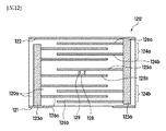
図14に示されるように、感電保護素子220がバリスタ単独素子のとき、感電保護素子220は、バリスタ物質層220b、220c及び内部電極225a、225bを含む。
As shown in FIG. 14, when the electric
前記感電保護素子220の下面は、回路基板14に実装するための外部電極221が備えられ、上面は導電性ガスケットまたはクリップ状の伝導体と連結するための連結電極222が備えられる。
The lower surface of the electric
このとき、前記感電保護素子220の両側には、前記外部電極221と連結電極222にそれぞれ連結される中間電極223a、223bが備えられる。即ち、中間電極223aは外部電極221と連結され、中間電極223bは連結電極222に連結される。選択的に、前記外部電極121と連結電極122は焼体120aの側面に備えられる。
At this time,
前記バリスタ物質層は、第1バリスタ物質層220b及び第2バリスタ物質層220cが交互に少なくとも2個の層からなる。ここで、前記第1バリスタ物質層220b及び前記第2バリスタ物質層220cは、ZnO、SrTiO3、BaTiO3、SiCの一つ以上を含む半導性材料、またはPr及びBi系材料のいずれか一つである。
The varistor material layer includes at least two layers of alternating first and second varistor material layers 220b and 220c. Here, the first
前記内部電極225a、225bは、第1バリスタ物質層221上に一定の間隔Lで離隔された複数の第1内部電極225aと、第2バリスタ物質層222上に一定の間隔Lで離隔された複数の第2内部電極225bとを含む。
The
ここで、バリスタ220の降伏電圧Vbrは、最も隣接した第1内部電極225aと第2内部電極225bと間にそれぞれ形成される降伏電圧の和である。
Here, the breakdown voltage Vbr of the
前記第1内部電極225a及び前記第2内部電極225bのそれぞれは、少なくとも一部が重ならないように配置される。即ち、前記第1内部電極225a及び前記第2内部電極225bのそれぞれは、少なくとも一部が重なるように交差配置されるか、互いに重ならないように相互間に交差配置される。
Each of the first internal electrode 225a and the second
また、前記第1内部電極または前記第2内部電極は、静電気またはリーク電流が内部電極225a、225bの隣接した位置に漏洩されなく、内部電極225a、225b間で正常に進むように間隔が設定されることが好ましい。
In addition, the first internal electrode or the second internal electrode is spaced so that static electricity or leakage current does not leak to a position adjacent to the
例えば、一つの第1内部電極225aと隣接する第2内部電極225bと間の離隔間隔Lは、前記第1内部電極225aと前記第2内部電極225b間の最短距離d1と前記隣接する他の第2内部電極225bと間の最短距離d2の和より大きく形成されることが好ましい。
For example, the separation distance L between one first internal electrode 225a and the adjacent second
図15に示されるように、感電保護素子220がキャパシタ層を備えたバリスタ複合素子のとき、感電保護素子220は感電保護部及びキャパシタ層224a、224bを含む。ここで、感電保護部は、バリスタ物質層220b、220c及び内部電極225a、225bを含む。
As shown in FIG. 15, when the electric
前記キャパシタ層224a、224bは、通信信号を通過させる少なくとも一つの積層キャパシタ層である。このようなキャパシタ層224a、224bは、感電保護部と電気的に並列で連結され、例えば、感電保護部の上部または下部に形成され、キャパシタ電極226a、226bを備える。 The capacitor layers 224a and 224b are at least one multilayer capacitor layer that allows communication signals to pass therethrough. Such capacitor layers 224a and 224b are electrically connected in parallel to the electric shock protection unit, and are formed, for example, on the upper or lower portion of the electric shock protection unit, and include capacitor electrodes 226a and 226b.
ここで、キャパシタ層224a、224bを形成するシート層220aは、複数のシート層が積層されたものであり、誘電率を有する絶縁体、例えば、セラミック材料からなる。このとき、セラミック材料は金属系酸化化合物であり、金属系酸化化合物は、Er2O3、Dy2O3、Ho2O3、V2O5、CoO、MoO3、SnO2、BaTiO3の中から選択された1種以上を含む。一方、上部キャパシタ層224aと下部キャパシタ層224bは同じ材料からなっていてもよいが、選択的に互いに異なる異種物質からなっていてもよい。 Here, the sheet layer 220a forming the capacitor layers 224a and 224b is formed by laminating a plurality of sheet layers, and is made of an insulator having a dielectric constant, for example, a ceramic material. At this time, the ceramic material is a metal-based oxide compound, and the metal-based oxide compounds are Er 2 O 3 , Dy 2 O 3 , Ho 2 O 3 , V 2 O 5 , CoO, MoO 3 , SnO 2 , and BaTiO 3 . Contains one or more selected from among them. On the other hand, the upper capacitor layer 224a and the lower capacitor layer 224b may be made of the same material, but may be selectively made of different substances.
また、前記第1内部電極または前記第2内部電極は、静電気またはリーク電流が内部電極225a、225bの隣接したキャパシタ電極226a、226bに漏洩されなく、内部電極225a、225b間で正常に進むように間隔が設定されることが好ましい。
In addition, the first internal electrode or the second internal electrode is configured so that static electricity or leakage current does not leak to the capacitor electrodes 226a and 226b adjacent to the
即ち、前記第1内部電極225a及び前記第2内部電極225bのそれぞれは、隣接したキャパシタ電極226a、226b間の距離が内部電極225a、225b間の離隔間隔Lより大きく形成されることが好ましい。
That is, each of the first internal electrode 225a and the second
図16〜図19に示されるように、感電保護用コンタクター200、200’は、導電性連結部がクリップ状の伝導体210の場合として、クリップ状の伝導体210は接触部211、延長部212及び端子部213を含む。
As shown in FIG. 16 to FIG. 19, the electric
接触部211は、湾曲部状を有し、図2に示されるように、伝導体12と電気的に接触できる。延長部212は、接触部211から延長形成され、弾性力を有する。端子部213は、前記感電保護部と電気的に連結される端子を含む。
The
このような接触部211、延長部212、及び端子部213は、弾性力を有する導電性物質で一体的に形成される。
The
前記感電保護素子120は、下面及び上面にそれぞれ外部電極121と連結電極122が形成される。このとき、図16に示されるように、感電保護素子120上面の連結電極122には、導電性接着層111が塗布されており、このような導電性接着層111を介してクリップ状の伝導体210が感電保護素子120の上部面に通電可能に設けられる。
The
別の実施例によれば、感電保護素子120は、図17〜図19に示されるように、上面に溝部1202が備えられる。ここで、感電保護素子120は、溝部1202の底面に連結電極122が備えられる。このとき、クリップ状の伝導体210は、少なくとも一部が溝部1202内に挿入結合され、導電性接着層111で位置固定される。
According to another embodiment, as shown in FIGS. 17 to 19, the electric
ここで、感電保護素子120は、その上面及び下面に外部電極121と連結電極122が形成されるとしたが、これに限定されなく、外部電極121と連結電極122は感電保護素子120の側面に備えられる。
Here, although the
このような構造により、前記溝部1202は、側面ストッパーの役割をすることができ、クリップ状の伝導体210に別途の側面ストッパーを備えなくてもよく、従って、製造費用を節減することができる。また、クリップ状の伝導体210の少なくとも一部が前記溝部1202に挿入されることによって、結合後、歪みや折れ曲げを防止し、特に、SMD後、リフロー工程で倒れるか、定位置から外れるのを防止することができる。
Due to such a structure, the
ここで、感電保護用コンタクター200は、クリップ状の伝導体210の下部に感電保護素子120が配置されたものを図示し、説明したが、これに限定されなく、クリップ状の伝導体210と感電保護素子120が電気的に直列連結される構造であってもよい。例えば、感電保護素子120は、端子部213と水平に配置される構造を有してもよく、この場合、端子部213は、回路基板14に接触されないように構成される。
Here, the electric
図20及び図21に示されるように、感電保護用コンタクター300、300’は、導電性連結部がシリコンゴムパッド310の場合であり、シリコンゴムパッド310は胴体311及び導電性ワイヤー312を含む。
As shown in FIGS. 20 and 21, in the electric
胴体311は、シリコンゴムからなり、その上部はアンテナまたはメタルハウジングのような伝導体12と面接触し、その下部は感電保護素子120に電気的に連結される。
The
導電性ワイヤー312は、胴体311内部に垂直形成される。このような導電性ワイヤー312は伝導体12との電気的接触を向上させると同時に、胴体311の弾性力を補完するためのものである。
The
例えば、導電性ワイヤー312は、伝導体12により加圧される場合、その上端が下側に曲がり、伝導体12が除去される場合、元来の垂直状態に復元されることによって、胴体311の弾性力を補完することができる。
For example, when the
図22に示されるように、前記感電保護用コンタクターは、導電性連結部が他の形態のシリコンゴムパッド320の場合であり、シリコンゴムパッド320は、胴体321、及び導電性ワイヤー322を含む。
As shown in FIG. 22, in the electric shock protection contactor, the conductive connection part is a
胴体321は、シリコンゴムからなり、その上部はアンテナまたはメタルハウジングのような伝導体12と面接触し、その下部はサプレッサー120に電気的に連結される。
The
導電性ワイヤー322は、胴体321内部から斜線に形成される。このような導電性ワイヤー322は、伝導体12との電気的接触を向上させると同時に、胴体321の弾性力を補完するためのものである。
The
例えば、導電性ワイヤー312は、伝導体12により加圧される場合、その上端が左右側に傾くと、伝導体12が除去される場合、元来の垂直状態に復元されることによって、胴体321の弾性力を補完することができる。このとき、伝導体12の加圧力により導電性ワイヤー312が傾けば、伝導体12との接触性に優れ、従って、通信信号の伝導性が向上される。
For example, when the
従って、このような導電性ワイヤー322は、伝導体12の加圧力により下側に曲がる、図20の垂直形成された導電性ワイヤー312に比べて、通信信号の伝導性に優れ、弾性復原力が良好であり、長期間使用が可能である。
Accordingly, such a
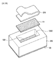
図23に示されるように、前記感電保護用コンタクターは、導電性連結部がシリコンゴムパッド330の場合であり、シリコンゴムパッド330は胴体331、伝導層332及び接触部333を含む。
As shown in FIG. 23, in the electric shock protection contactor, the conductive connection part is a
胴体331はシリコンゴムからなり、その下部は感電保護素子120に電気的に連結される。
The
伝導層332は、胴体331の内部から水平に交差積層され、硬化型Agペーストからなる複数の層である。このような伝導層332は、伝導体12との電気的接触を向上させると同時に、胴体331の弾性力を補完するためのものである。
The
例えば、伝導層332は、伝導体12により加圧される場合、その中央部付近から下側に押圧され、伝導体12が除去される場合、元来の水平状態に復元されることによって、胴体331の弾性力を補完することができる。従って、このような伝導層332は、伝導体12の加圧力により下側に曲がる図20の垂直形成された導電性ワイヤー312または左右側に傾く図22の斜線形成された導電性ワイヤー322に比べて、弾性復原力に優れ、長期間使用が可能である。
For example, when the
接触部333は、胴体332の上側に曲線突起状に形成される。このような接触部333は、アンテナまたはメタルハウジングのような導体12と多数の線または面接触することによって、伝導体12との接触面積を増大させる。従って、シリコンゴムパッド330は、通信信号の伝導性が向上される。
The
前述したような感電保護用コンタクターは、携帯用電子装置において、人体接触可能な伝導体12と回路基板14と上に配置される。ここで、前記感電保護用コンタクターは、回路基板14の実装用端子上に実装される。
The contactor for electric shock protection as described above is disposed on the
このような配置により、前記携帯用電子装置は、回路基板14の接地から流入される外部電源によるリーク電流を遮断することによって、外部電源によるリーク電流から使用者を保護することができ、これと共に、伝導体12から静電気流入時、絶縁破壊なしで静電気を通過させ、伝導体12から流入される通信信号を減殺することなく通過させることによって、静電気から内部回路を保護し、高いキャパシタンスを具現することができる。
With such an arrangement, the portable electronic device can protect the user from the leakage current due to the external power source by blocking the leakage current due to the external power source flowing from the ground of the
以上で、本発明の一実施例について説明したが、本発明の思想は本、明細書に提示される実施例に制限されなく、本発明の思想を理解する当業者であれば同一思想の範囲内で、構成要素の付加、変更、削除、追加などによって他の実施例を容易に提案することができるが、これもまた本発明の思想範囲内に属するものである。 Although one embodiment of the present invention has been described above, the idea of the present invention is not limited to the embodiment presented in this specification, and those skilled in the art who understand the idea of the present invention will be within the scope of the same idea. In the above, other embodiments can be easily proposed by adding, changing, deleting, adding components, and the like, and this also falls within the spirit of the present invention.
Claims (31)
導電性接着層を介して前記導電性連結部に直列連結され、前記電子装置の回路基板の接地から流入される外部電源のリーク電流を遮断する感電保護素子と、を含む感電保護用コンタクター。 An electrically conductive coupling having an elastic force for making electrical contact with the conductor of the electronic device;
An electric shock protection contactor comprising: an electric shock protection element that is connected in series to the conductive connection portion via a conductive adhesive layer and blocks leakage current of an external power source that flows in from a ground of a circuit board of the electronic device.
前記導電性連結部に直列連結され、前記電子装置の回路基板の接地から流入される外部電源のリーク電流を遮断する感電保護素子と、を含み、
前記感電保護素子は、上側に溝部を備え、
前記導電性連結部は、前記溝部に少なくとも一部が挿入される感電保護用コンタクター。 An electrically conductive coupling having an elastic force for making electrical contact with the conductor of the electronic device;
An electrical protection element that is connected in series to the conductive connection part and blocks leakage current of an external power source that flows in from the ground of the circuit board of the electronic device;
The electric shock protection element has a groove on the upper side,
The conductive connection part is an electric shock protection contactor in which at least a part is inserted into the groove part.
前記導電性連結部に直列連結され、前記電子装置の回路基板の接地から流入される外部電源のリーク電流を遮断する感電保護素子と、を含み、
前記感電保護素子は、下記数式(1)を満たす降伏電圧Vbrを有する感電保護用コンタクター:
An electrical protection element that is connected in series to the conductive connection part and blocks leakage current of an external power source that flows in from the ground of the circuit board of the electronic device;
The electric shock protection element has a breakdown voltage Vbr satisfying the following mathematical formula (1):
前記感電保護部は、下記式を満たす降伏電圧Vbrを有する請求項2または請求項4に記載の感電保護用コンタクター:
Vcpは、前記キャパシタ層の絶縁破壊電圧である。) The electric shock protection element includes an electric shock protection unit and at least one capacitor layer,
The electric shock protection contactor according to claim 2, wherein the electric shock protection unit has a breakdown voltage Vbr satisfying the following formula:
Vcp is a breakdown voltage of the capacitor layer. )
シリコンゴムからなる胴体と、
前記胴体内部に垂直形成される導電性ワイヤーと、
を含む請求項7に記載の感電保護用コンタクター。 The silicone rubber pad is
A body made of silicone rubber;
A conductive wire vertically formed inside the fuselage;
The contactor for electric shock protection of Claim 7 containing.
シリコンゴムからなる胴体と、
前記胴体内部に斜線で形成された導電性ワイヤーと、
を含む請求項7に記載の感電保護用コンタクター。 The silicone rubber pad is
A body made of silicone rubber;
A conductive wire formed with diagonal lines inside the fuselage;
The contactor for electric shock protection of Claim 7 containing.
シリコンゴムからなる胴体と、
前記胴体内部に水平に交差積層された複数の伝導層と、
前記胴体の上側に曲線突起状に形成された複数の接触部と、
を含む請求項7に記載の感電保護用コンタクター。 The silicone rubber pad is
A body made of silicone rubber;
A plurality of conductive layers horizontally cross-laminated within the fuselage;
A plurality of contact portions formed in a curved protrusion shape on the upper side of the body;
The contactor for electric shock protection of Claim 7 containing.
湾曲部状を有し、前記接触する伝導体と接触する接触部と、
前記接触部から延長形成され、弾性力を有する延長部と、
前記感電保護素子と電気的に連結される端子部と、
を含む請求項7に記載の感電保護用コンタクター。 The clip-shaped conductor is:
A contact portion having a curved portion shape and in contact with the contacting conductor;
An extension formed from the contact portion and having an elastic force;
A terminal portion electrically connected to the electric shock protection element;
The contactor for electric shock protection of Claim 7 containing.
前記導電性連結部は、導電性接着層を介して前記外部電極上に積層される請求項4に記載の感電保護用コンタクター。 The electric shock protection element is provided with an external electrode on the bottom surface of the groove,
The contactor for electric shock protection according to claim 4, wherein the conductive connecting portion is laminated on the external electrode via a conductive adhesive layer.
複数のシート層が積層された焼体と、
前記焼体の内部に、一定の間隔で離隔され形成された少なくとも一対の内部電極と、を含む請求項1、4及び5のいずれか一項に記載の感電保護用コンタクター。 The electric shock protection element is
A fired body in which a plurality of sheet layers are laminated;
The contactor for electric shock protection according to any one of claims 1, 4 and 5, comprising at least a pair of internal electrodes formed at a predetermined interval inside the fired body.
前記空隙は、内壁に高さ方向に沿って一定の厚さで塗布される放電物質層が備えられる請求項14に記載の感電保護用コンタクター。 Further comprising a gap formed between the internal electrodes,
The contactor for electric shock protection according to claim 14, wherein the gap is provided with a discharge material layer applied to the inner wall with a constant thickness along the height direction.
第1バリスタ物質層と第2バリスタ物質層とが交互に積層された少なくとも2個のバリスタ物質層と、
前記第1バリスタ物質層上に一定の間隔Lで離隔された複数の第1内部電極と、
前記第2バリスタ物質層上に一定の間隔Lで離隔された複数の第2内部電極と、
を含む請求項1または請求項4に記載の感電保護用コンタクター。 The electric shock protection element is
At least two varistor material layers in which first varistor material layers and second varistor material layers are alternately stacked;
A plurality of first internal electrodes spaced apart from each other by a predetermined distance L on the first varistor material layer;
A plurality of second internal electrodes spaced apart from each other by a predetermined distance L on the second varistor material layer;
The contactor for electric shock protection of Claim 1 or Claim 4 containing this.
第1バリスタ物質層と第2バリスタ物質層とが交互に積層された少なくとも2個のバリスタ物質層と、
前記第1バリスタ物質層上に一定の間隔Lで離隔された複数の第1内部電極と、
前記第2バリスタ物質層上に一定の間隔Lで離隔された複数の第2内部電極と、
を含み、
前記降伏電圧Vbrは、最も隣接した第1内部電極と第2内部電極と間にそれぞれ形成される降伏電圧の和である請求項5に記載の感電保護用コンタクター。 The electric shock protection element is
At least two varistor material layers in which first varistor material layers and second varistor material layers are alternately stacked;
A plurality of first internal electrodes spaced apart from each other by a predetermined distance L on the first varistor material layer;
A plurality of second internal electrodes spaced apart from each other by a predetermined distance L on the second varistor material layer;
Including
The contactor for electric shock protection according to claim 5 , wherein the breakdown voltage Vbr is a sum of breakdown voltages respectively formed between a first internal electrode and a second internal electrode that are closest to each other.
複数のシート層が積層された焼体と、
前記焼体の内部に、一定の間隔で離隔され形成された少なくとも一対の内部電極を含む感電保護部と、
前記通信信号を通過させる少なくとも一つの積層キャパシタ層と、
を含む請求項6に記載の感電保護用コンタクター。 The electric shock protection element is
A fired body in which a plurality of sheet layers are laminated;
An electric shock protection unit including at least a pair of internal electrodes formed at a predetermined interval inside the fired body,
At least one multilayer capacitor layer through which the communication signal passes;
The contactor for electric shock protection according to claim 6 comprising:
前記空隙は、内壁に高さ方向に沿って一定の厚さで塗布される放電物質層が備えられる請求項23に記載の感電保護用コンタクター。 The electric shock protection part further includes a gap formed between the internal electrodes,
The contactor for electric shock protection according to claim 23, wherein the gap is provided with a discharge material layer applied to the inner wall at a constant thickness along the height direction.
第1バリスタ物質層と第2バリスタ物質層とが交互に積層された少なくとも2個のバリスタ物質層と、前記第1バリスタ物質層上に一定の間隔Lで離隔された複数の第1内部電極と、前記第2バリスタ物質層上に一定の間隔Lで離隔された複数の第2内部電極とを含む感電保護部と、
前記通信信号を通過させる少なくとも一つの積層キャパシタ層と、
を含む請求項6に記載の感電保護用コンタクター。 The electric shock protection element is
At least two varistor material layers in which a first varistor material layer and a second varistor material layer are alternately stacked; and a plurality of first internal electrodes spaced apart from each other by a predetermined distance L on the first varistor material layer; A plurality of second internal electrodes spaced apart from each other by a predetermined distance L on the second varistor material layer;
At least one multilayer capacitor layer through which the communication signal passes;
The contactor for electric shock protection according to claim 6 comprising:
複数個の手動素子及び能動素子が設けられる回路基板と、
一端は前記回路基板と電気的に連結され、他端は前記伝導体と電気的に直列連結される感電保護用コンタクターと、を含み、
前記感電保護用コンタクターは、
前記伝導体に電気的に接触する導電性連結部と、
前記導電性連結部に直列連結され、前記回路基板の接地から流入される外部電源のリーク電流を遮断する感電保護素子と、を含み、
前記感電保護素子は、下記数式(1)を満たす降伏電圧Vbrを有する携帯用電子装置:
A circuit board provided with a plurality of manual elements and active elements;
One end is electrically connected to the circuit board and the other end is electrically connected to the conductor in series with an electric shock protection contactor;
The electric shock protection contactor is:
A conductive connecting portion in electrical contact with the conductor;
An electrical protection element that is connected in series to the conductive connection portion and blocks leakage current of an external power source that flows in from the ground of the circuit board;
The electric shock protection element has a breakdown voltage Vbr satisfying the following mathematical formula (1):
Applications Claiming Priority (3)
| Application Number | Priority Date | Filing Date | Title |
|---|---|---|---|
| KR10-2015-0094280 | 2015-07-01 | ||
| KR1020150094280A KR101585604B1 (en) | 2015-07-01 | 2015-07-01 | Circuit protection contactor and mobile electronic device with the same |
| PCT/KR2015/007123 WO2017003001A1 (en) | 2015-07-01 | 2015-07-09 | Electric shock-preventing contactor and portable electronic device having same |
Publications (2)
| Publication Number | Publication Date |
|---|---|
| JP2017529680A JP2017529680A (en) | 2017-10-05 |
| JP6449286B2 true JP6449286B2 (en) | 2019-01-09 |
Family
ID=55173204
Family Applications (1)
| Application Number | Title | Priority Date | Filing Date |
|---|---|---|---|
| JP2016534239A Active JP6449286B2 (en) | 2015-07-01 | 2015-07-09 | Contactor for electric shock protection and portable electronic device having the same |
Country Status (6)
| Country | Link |
|---|---|
| US (1) | US10188019B2 (en) |
| EP (1) | EP3128620B1 (en) |
| JP (1) | JP6449286B2 (en) |
| KR (1) | KR101585604B1 (en) |
| CN (2) | CN105470685B (en) |
| WO (1) | WO2017003001A1 (en) |
Families Citing this family (31)
| Publication number | Priority date | Publication date | Assignee | Title |
|---|---|---|---|---|
| KR101939650B1 (en) * | 2015-07-01 | 2019-01-17 | 주식회사 아모텍 | Functional circuit protection contactor and potable electronic device with the same |
| KR20170031010A (en) * | 2015-09-10 | 2017-03-20 | 조인셋 주식회사 | Method for producing composite filter |
| WO2017105074A1 (en) | 2015-12-16 | 2017-06-22 | 주식회사 아모텍 | Electronic device contactor coupling structure and portable electronic device including same |
| KR101947440B1 (en) * | 2016-02-04 | 2019-05-10 | 주식회사 아모텍 | Clip type contactor and protection device having the same |
| WO2017146435A1 (en) * | 2016-02-24 | 2017-08-31 | 주식회사 아모텍 | Guide-connected contactor and portable electronic device comprising same |
| KR101977270B1 (en) * | 2016-02-24 | 2019-05-10 | 주식회사 아모텍 | Contactor with guide and mobile electronic apparatus with the same |
| KR101727080B1 (en) * | 2016-02-24 | 2017-05-02 | 주식회사 아모텍 | Contactor with guide and mobile electronic apparatus with the same |
| US10756472B2 (en) | 2016-02-26 | 2020-08-25 | Amotech Co., Ltd. | Functional contactor and portable electronic device comprising same |
| WO2017146517A1 (en) * | 2016-02-26 | 2017-08-31 | 주식회사 아모텍 | Functional contactor and portable electronic device comprising same |
| KR102503223B1 (en) | 2016-03-10 | 2023-02-24 | 삼성전자주식회사 | Connecting member and electronic device comprising thereof |
| WO2017196116A1 (en) * | 2016-05-12 | 2017-11-16 | 주식회사 아모텍 | Functional contactor |
| KR101947425B1 (en) | 2016-05-12 | 2019-02-13 | 주식회사 아모텍 | Functional contactor |
| WO2017196149A1 (en) * | 2016-05-13 | 2017-11-16 | 주식회사 모다이노칩 | Contactor, and electronic device provided with same |
| KR101842211B1 (en) * | 2016-05-13 | 2018-05-14 | 주식회사 모다이노칩 | Contactor for preventing electric shock and electronic device having the same |
| WO2017196151A1 (en) * | 2016-05-13 | 2017-11-16 | 주식회사 모다이노칩 | Contactor, and electronic device provided with same |
| WO2017196150A1 (en) * | 2016-05-13 | 2017-11-16 | 주식회사 모다이노칩 | Contactor, and electronic device provided with same |
| KR101738984B1 (en) * | 2016-05-26 | 2017-05-24 | 주식회사 모다이노칩 | Contactor for preventing |
| KR20170133733A (en) * | 2016-05-26 | 2017-12-06 | 주식회사 모다이노칩 | Contactor for preventing electric shock |
| KR20170135146A (en) | 2016-05-30 | 2017-12-08 | 주식회사 모다이노칩 | Contactor for preventing electric shock |
| KR101751825B1 (en) | 2016-06-17 | 2017-07-11 | 조인셋 주식회사 | Antenna Bandwidth Expander having protecting electric shock |
| CN207719393U (en) | 2016-06-21 | 2018-08-10 | 株式会社村田制作所 | Portable radio terminal |
| KR101789243B1 (en) * | 2016-10-07 | 2017-11-20 | 주식회사 모다이노칩 | Complex protection device and electronic device having the same |
| US11094777B2 (en) | 2016-11-04 | 2021-08-17 | Amotech Co., Ltd. | Functional contactor |
| WO2018084587A1 (en) * | 2016-11-04 | 2018-05-11 | 주식회사 아모텍 | Functional contactor |
| KR102586947B1 (en) * | 2016-11-09 | 2023-10-10 | 주식회사 아모텍 | Functional contactor and mobile electronic apparatus with the same |
| KR102565034B1 (en) * | 2016-11-09 | 2023-08-09 | 주식회사 아모텍 | Functional contactor |
| KR101828990B1 (en) * | 2016-12-01 | 2018-02-14 | 주식회사 모다이노칩 | Complex protection device and electronic device having the same |
| CN110100355B (en) * | 2016-12-21 | 2022-01-25 | 阿莫技术有限公司 | Functional contactor |
| KR101958775B1 (en) * | 2016-12-23 | 2019-03-18 | 주식회사 모다이노칩 | Complex protection device and electronic device having the same |
| US20240105366A1 (en) * | 2019-11-08 | 2024-03-28 | Tdk Electronics Ag | Varistor |
| CN111495679B (en) * | 2020-04-28 | 2021-12-07 | 南兴装备股份有限公司 | Method for monitoring leakage condition of gluing mechanism of edge bonding machine |
Family Cites Families (41)
| Publication number | Priority date | Publication date | Assignee | Title |
|---|---|---|---|---|
| JPS6210981Y2 (en) * | 1980-07-02 | 1987-03-16 | ||
| JPS57207324A (en) * | 1981-06-16 | 1982-12-20 | Matsushita Electric Ind Co Ltd | Composite function element |
| US4461980A (en) * | 1982-08-25 | 1984-07-24 | Nilssen Ole K | Protection circuit for series resonant electronic ballasts |
| JP2535510B2 (en) * | 1986-07-26 | 1996-09-18 | ティーディーケイ株式会社 | Noise absorber |
| JP2643193B2 (en) * | 1987-10-20 | 1997-08-20 | 株式会社村田製作所 | 3-terminal multi-function device |
| JPH01183803A (en) * | 1988-01-19 | 1989-07-21 | Murata Mfg Co Ltd | Composite electronic part |
| US4811164A (en) * | 1988-03-28 | 1989-03-07 | American Telephone And Telegraph Company, At&T Bell Laboratories | Monolithic capacitor-varistor |
| GB2242066B (en) * | 1990-03-16 | 1994-04-27 | Ecco Ltd | Varistor structures |
| US5139442A (en) * | 1990-12-03 | 1992-08-18 | Murata Manufacturing Co., Ltd. | Modular jack |
| US5528079A (en) * | 1991-12-23 | 1996-06-18 | Gi Corporation | Hermetic surface mount package for a two terminal semiconductor device |
| JPH06231837A (en) * | 1993-02-04 | 1994-08-19 | Murata Mfg Co Ltd | Connector |
| JP2586321Y2 (en) * | 1993-11-02 | 1998-12-02 | 信越ポリマー株式会社 | Elastic anisotropic conductive connector with holder |
| JP2586321B2 (en) * | 1994-02-22 | 1997-02-26 | 三菱マテリアル株式会社 | Manufacturing method of building materials |
| JPH10199709A (en) * | 1997-01-09 | 1998-07-31 | Tdk Corp | Multilayer type varistor |
| JP2000188169A (en) * | 1998-12-21 | 2000-07-04 | Tokin Corp | Surge absorbing element |
| DE10147898A1 (en) | 2001-09-28 | 2003-04-30 | Epcos Ag | Electrochemical component with multiple contact surfaces |
| DE10354220A1 (en) * | 2003-11-20 | 2005-06-30 | Kolektor D.O.O. | Commutator for an electric machine |
| KR100689549B1 (en) | 2003-12-08 | 2007-03-02 | 삼성전자주식회사 | Apparatus for intercepting a leakage of electricity and electromagnetic wave in the mobile terminal |
| KR100809249B1 (en) * | 2006-05-10 | 2008-02-29 | 삼성전기주식회사 | Built-in Antenna Assembly of Wireless Communication Terminals |
| KR100856236B1 (en) * | 2006-05-10 | 2008-09-03 | 삼성전기주식회사 | Built-in Antenna Assembly of Wireless Communication Terminals |
| JP2007329322A (en) * | 2006-06-08 | 2007-12-20 | Canon Inc | Shielding case fitting structure |
| KR100846343B1 (en) * | 2006-10-27 | 2008-07-15 | 삼성전자주식회사 | Built-in antenna module for portable wireless terminal |
| KR101326653B1 (en) | 2007-01-17 | 2013-11-08 | 엘지전자 주식회사 | Portable terminal |
| KR20080044551A (en) | 2006-11-16 | 2008-05-21 | 엘지전자 주식회사 | Mobile communication terminal |
| KR20080001363U (en) * | 2006-11-22 | 2008-05-27 | 리 듀오 인터내셔널 컴퍼니 리미티드 | Improvement of rubber connector |
| US20100254052A1 (en) * | 2007-11-27 | 2010-10-07 | Hidenori Katsumura | Static electricity countermeasure component and method for manufacturing the static electricity countermeasure component |
| JPWO2010061519A1 (en) * | 2008-11-26 | 2012-04-19 | 株式会社村田製作所 | ESD protection device and manufacturing method thereof |
| JP2010146779A (en) * | 2008-12-17 | 2010-07-01 | Panasonic Corp | Overvoltage protection component |
| CN101958534B (en) * | 2009-07-15 | 2015-04-15 | 中山市云创知识产权服务有限公司 | Electrostatic discharge module and mobile communication device with electrostatic discharge module |
| JP2012033654A (en) * | 2010-07-29 | 2012-02-16 | Tdk Corp | Ceramic capacitor |
| JP2012033652A (en) * | 2010-07-29 | 2012-02-16 | Tdk Corp | Ceramic capacitor |
| TWI404485B (en) * | 2010-12-02 | 2013-08-01 | Quanta Comp Inc | Method of assembling an electric device and the electric device |
| KR101915961B1 (en) * | 2011-09-06 | 2019-01-31 | 삼성전자주식회사 | electronic device and board usable in the electronic device |
| KR101364117B1 (en) | 2012-05-17 | 2014-02-19 | 이중식 | Antenna Contactor For Mobile Communication Terminal And Method For Providing The Contactor |
| DE102012014860A1 (en) * | 2012-07-26 | 2014-05-15 | Infineon Technologies Ag | ESD protection |
| JP5950204B2 (en) * | 2012-09-28 | 2016-07-13 | パナソニックIpマネジメント株式会社 | Wireless communication module |
| JP6032212B2 (en) * | 2013-03-19 | 2016-11-24 | 株式会社村田製作所 | Multilayer electronic component and its mounting structure |
| CN203522281U (en) * | 2013-10-31 | 2014-04-02 | 吴枫 | Mobile phone charger |
| JP6272196B2 (en) * | 2014-09-25 | 2018-01-31 | 京セラ株式会社 | Multilayer capacitor |
| US10631448B2 (en) * | 2015-01-29 | 2020-04-21 | Amotech Co., Ltd. | Portable electronic device with embedded electric shock protection function |
| EP3142470A1 (en) * | 2015-09-10 | 2017-03-15 | Joinset Co., Ltd | Elastic composite filter |
-
2015
- 2015-07-01 KR KR1020150094280A patent/KR101585604B1/en active IP Right Grant
- 2015-07-09 JP JP2016534239A patent/JP6449286B2/en active Active
- 2015-07-09 EP EP15831206.6A patent/EP3128620B1/en active Active
- 2015-07-09 WO PCT/KR2015/007123 patent/WO2017003001A1/en active Application Filing
- 2015-10-16 US US14/885,549 patent/US10188019B2/en active Active
- 2015-11-18 CN CN201510794278.5A patent/CN105470685B/en active Active
- 2015-11-18 CN CN201810202200.3A patent/CN108598755B/en active Active
Also Published As
| Publication number | Publication date |
|---|---|
| KR101585604B1 (en) | 2016-01-14 |
| US20170005464A1 (en) | 2017-01-05 |
| EP3128620A1 (en) | 2017-02-08 |
| EP3128620A4 (en) | 2018-02-21 |
| WO2017003001A1 (en) | 2017-01-05 |
| CN108598755B (en) | 2022-05-10 |
| EP3128620B1 (en) | 2019-09-18 |
| JP2017529680A (en) | 2017-10-05 |
| US10188019B2 (en) | 2019-01-22 |
| CN105470685A (en) | 2016-04-06 |
| CN105470685B (en) | 2018-04-13 |
| CN108598755A (en) | 2018-09-28 |
Similar Documents
| Publication | Publication Date | Title |
|---|---|---|
| JP6449286B2 (en) | Contactor for electric shock protection and portable electronic device having the same | |
| US10635138B2 (en) | Electric shock protection device and portable electronic device including the same | |
| KR102108900B1 (en) | Circuit protection device | |
| JP6352419B2 (en) | ELECTRIC SHOCK PROTECTION ELEMENT AND PORTABLE ELECTRONIC DEVICE HAVING THE SAME | |
| KR101578544B1 (en) | Circuit protection device and mobile electronic device with the same | |
| CN108701943B (en) | Functional contactor and portable electronic device comprising same | |
| KR101638053B1 (en) | Contactor and mobile electronic device with the same | |
| KR20170060846A (en) | Circuit protection contactor and mobile electronic device with the same | |
| US10231366B2 (en) | Electric shock prevention apparatus | |
| KR101969023B1 (en) | Electric shock protection contactor assembly and mobile electronic apparatus with the same | |
| KR20170069036A (en) | Circuit protection contactor and mobile electronic device with the same | |
| KR102586947B1 (en) | Functional contactor and mobile electronic apparatus with the same | |
| KR101916156B1 (en) | Electric shock protection device | |
| KR101939658B1 (en) | Electric shock protection contactor assembly and mobile electronic apparatus with the same | |
| KR20170004797A (en) | Circuit protection contactor and mobile electronic device with the same | |
| KR20170060878A (en) | Circuit protection contactor and mobile electronic device with the same | |
| KR20170051068A (en) | Electric shock protection contactor and mobile electronic device with the same | |
| KR20170060848A (en) | Circuit protection contactor and mobile electronic device with the same | |
| KR20170053052A (en) | Electric shock protection contactor and mobile electronic device with the same | |
| KR20170053049A (en) | Electric shock protection contactor and mobile electronic device with the same | |
| KR20170048986A (en) | Circuit protection contactor and mobile electronic device with the same | |
| KR20170048985A (en) | Circuit protection contactor and mobile electronic device with the same | |
| KR20170060881A (en) | Circuit protection contactor and mobile electronic device with the same | |
| KR20170059780A (en) | Circuit protection contactor and mobile electronic device with the same | |
| KR20170060886A (en) | Circuit protection contactor and mobile electronic device with the same |
Legal Events
| Date | Code | Title | Description |
|---|---|---|---|
| A131 | Notification of reasons for refusal |
Free format text: JAPANESE INTERMEDIATE CODE: A131 Effective date: 20170905 |
|
| A521 | Request for written amendment filed |
Free format text: JAPANESE INTERMEDIATE CODE: A523 Effective date: 20171204 |
|
| A131 | Notification of reasons for refusal |
Free format text: JAPANESE INTERMEDIATE CODE: A131 Effective date: 20180605 |
|
| TRDD | Decision of grant or rejection written | ||
| A01 | Written decision to grant a patent or to grant a registration (utility model) |
Free format text: JAPANESE INTERMEDIATE CODE: A01 Effective date: 20181127 |
|
| A61 | First payment of annual fees (during grant procedure) |
Free format text: JAPANESE INTERMEDIATE CODE: A61 Effective date: 20181205 |
|
| R150 | Certificate of patent or registration of utility model |
Ref document number: 6449286 Country of ref document: JP Free format text: JAPANESE INTERMEDIATE CODE: R150 |
|
| R250 | Receipt of annual fees |
Free format text: JAPANESE INTERMEDIATE CODE: R250 |
|
| R250 | Receipt of annual fees |
Free format text: JAPANESE INTERMEDIATE CODE: R250 |
|
| R250 | Receipt of annual fees |
Free format text: JAPANESE INTERMEDIATE CODE: R250 |