JP6439552B2 - Semiconductor module and semiconductor device - Google Patents
Semiconductor module and semiconductor device Download PDFInfo
- Publication number
- JP6439552B2 JP6439552B2 JP2015075251A JP2015075251A JP6439552B2 JP 6439552 B2 JP6439552 B2 JP 6439552B2 JP 2015075251 A JP2015075251 A JP 2015075251A JP 2015075251 A JP2015075251 A JP 2015075251A JP 6439552 B2 JP6439552 B2 JP 6439552B2
- Authority
- JP
- Japan
- Prior art keywords
- plate
- semiconductor
- semiconductor module
- gate
- guide groove
- Prior art date
- Legal status (The legal status is an assumption and is not a legal conclusion. Google has not performed a legal analysis and makes no representation as to the accuracy of the status listed.)
- Expired - Fee Related
Links
Images


Classifications
-
- H—ELECTRICITY
- H10—SEMICONDUCTOR DEVICES; ELECTRIC SOLID-STATE DEVICES NOT OTHERWISE PROVIDED FOR
- H10W—GENERIC PACKAGES, INTERCONNECTIONS, CONNECTORS OR OTHER CONSTRUCTIONAL DETAILS OF DEVICES COVERED BY CLASS H10
- H10W40/00—Arrangements for thermal protection or thermal control
- H10W40/40—Arrangements for thermal protection or thermal control involving heat exchange by flowing fluids
- H10W40/47—Arrangements for thermal protection or thermal control involving heat exchange by flowing fluids by flowing liquids, e.g. forced water cooling
-
- H—ELECTRICITY
- H10—SEMICONDUCTOR DEVICES; ELECTRIC SOLID-STATE DEVICES NOT OTHERWISE PROVIDED FOR
- H10D—INORGANIC ELECTRIC SEMICONDUCTOR DEVICES
- H10D64/00—Electrodes of devices having potential barriers
- H10D64/20—Electrodes characterised by their shapes, relative sizes or dispositions
- H10D64/27—Electrodes not carrying the current to be rectified, amplified, oscillated or switched, e.g. gates
- H10D64/311—Gate electrodes for field-effect devices
- H10D64/411—Gate electrodes for field-effect devices for FETs
- H10D64/511—Gate electrodes for field-effect devices for FETs for IGFETs
- H10D64/512—Disposition of the gate electrodes, e.g. buried gates
-
- H—ELECTRICITY
- H10—SEMICONDUCTOR DEVICES; ELECTRIC SOLID-STATE DEVICES NOT OTHERWISE PROVIDED FOR
- H10W—GENERIC PACKAGES, INTERCONNECTIONS, CONNECTORS OR OTHER CONSTRUCTIONAL DETAILS OF DEVICES COVERED BY CLASS H10
- H10W72/00—Interconnections or connectors in packages
-
- H—ELECTRICITY
- H10—SEMICONDUCTOR DEVICES; ELECTRIC SOLID-STATE DEVICES NOT OTHERWISE PROVIDED FOR
- H10W—GENERIC PACKAGES, INTERCONNECTIONS, CONNECTORS OR OTHER CONSTRUCTIONAL DETAILS OF DEVICES COVERED BY CLASS H10
- H10W72/00—Interconnections or connectors in packages
- H10W72/50—Bond wires
-
- H—ELECTRICITY
- H10—SEMICONDUCTOR DEVICES; ELECTRIC SOLID-STATE DEVICES NOT OTHERWISE PROVIDED FOR
- H10W—GENERIC PACKAGES, INTERCONNECTIONS, CONNECTORS OR OTHER CONSTRUCTIONAL DETAILS OF DEVICES COVERED BY CLASS H10
- H10W76/00—Containers; Fillings or auxiliary members therefor; Seals
- H10W76/10—Containers or parts thereof
- H10W76/12—Containers or parts thereof characterised by their shape
- H10W76/13—Containers comprising a conductive base serving as an interconnection
- H10W76/136—Containers comprising a conductive base serving as an interconnection having other interconnections perpendicular to the conductive base
-
- H—ELECTRICITY
- H10—SEMICONDUCTOR DEVICES; ELECTRIC SOLID-STATE DEVICES NOT OTHERWISE PROVIDED FOR
- H10W—GENERIC PACKAGES, INTERCONNECTIONS, CONNECTORS OR OTHER CONSTRUCTIONAL DETAILS OF DEVICES COVERED BY CLASS H10
- H10W90/00—Package configurations
Landscapes
- Inverter Devices (AREA)
- Power Conversion In General (AREA)
Description
本発明は、半導体モジュール及びそれを備えた半導体装置に関する。 The present invention relates to a semiconductor module and a semiconductor device including the same.
半導体装置の一つとして、IGBT(Insulated Gate Bipolar Transistor)、FWD(Free Wheeling Diode)等の複数の半導体素子を含む半導体モジュールが広く用いられている。例えば、この半導体モジュールを並列接続することで、スイッチング、コンバータ等としての機能が実現される。このような半導体モジュールの内、モジュール内部に絶縁機能を有さない非絶縁型の半導体モジュールは、絶縁型の半導体モジュールに比べ、内部配線のインダクタンスを低減することができる。 As one of semiconductor devices, a semiconductor module including a plurality of semiconductor elements such as an insulated gate bipolar transistor (IGBT) and a free wheeling diode (FWD) is widely used. For example, by connecting the semiconductor modules in parallel, functions as switching, a converter, and the like are realized. Among such semiconductor modules, a non-insulating semiconductor module that does not have an insulating function inside the module can reduce the inductance of the internal wiring as compared with the insulating semiconductor module.
非絶縁型の半導体モジュールは、上面にゲート端子とソース端子を備え、下面にドレイン端子を備えている。そして、上面からゲート導体とソース導体が一体になったものを配置し、下面にドレイン導体を配置し、それらを上下から圧接することにより、外部と電気的に接続されている(例えば、特許文献1参照)。 The non-insulating semiconductor module includes a gate terminal and a source terminal on the upper surface and a drain terminal on the lower surface. Then, the gate conductor and the source conductor are integrated from the upper surface, the drain conductor is disposed on the lower surface, and they are pressed from above and below to be electrically connected to the outside (for example, Patent Documents) 1).
しかし、特許文献1の半導体モジュールでは、ゲート導体に圧接されたばね板形状のゲート端子は、半導体モジュールの動作中にゲート導体が摺動して、ゲート導体との接触面の電気抵抗が増加する。このため、半導体モジュールに動作不良が生じてしまうおそれがある。
However, in the semiconductor module of
本発明は、このような点を鑑みてなされたものであり、動作不良の発生が抑制された半導体を提供することを目的とする。 The present invention has been made in view of such a point, and an object thereof is to provide a semiconductor in which the occurrence of malfunction is suppressed.
本発明の一観点によれば、ドレイン板と、おもて面にゲート電極とソース電極とを備え、裏面にドレイン電極を備え、前記ドレイン板のおもて面に配置され、前記ドレイン電極と前記ドレイン板が電気的に接続される半導体素子と、絶縁板と、前記絶縁板のおもて面に設けられた第1回路板及び第2回路板を備え、前記ドレイン板のおもて面に配置され、前記第1回路板は前記ゲート電極と電気的に接続され、前記第2回路板は前記ソース電極と電気的に接続された、積層基板と、前記第1回路板上に配置されたゲート端子と、前記第2回路板上に配置されたソース端子と、開口及びガイド溝を備え、前記ドレイン板のおもて面と対向して配置され、前記ゲート端子及び前記ソース端子が前記開口に位置し、前記ガイド溝は前記開口に接して外周部に延伸されている、蓋と、を備える半導体モジュールが提供される。 According to one aspect of the present invention, the drain plate includes a gate electrode and a source electrode on the front surface, a drain electrode on the back surface, and is disposed on the front surface of the drain plate. A semiconductor element to which the drain plate is electrically connected, an insulating plate, and a first circuit board and a second circuit board provided on the front surface of the insulating plate, the front surface of the drain plate The first circuit board is electrically connected to the gate electrode, and the second circuit board is electrically connected to the source electrode, and is disposed on the first circuit board. A gate terminal, a source terminal disposed on the second circuit board, an opening and a guide groove, and disposed to face the front surface of the drain plate, wherein the gate terminal and the source terminal are The guide groove is in contact with the opening. Is stretched in the circumferential portion, and the lid, a semiconductor module with supplied.
開示の技術によれば、半導体装置の動作不良の発生を防止して、半導体装置の特性の低下を抑制することができるようになる。 According to the disclosed technology, it is possible to prevent the malfunction of the semiconductor device and to suppress the deterioration of the characteristics of the semiconductor device.
以下、図面を参照して実施の形態について説明する。
[第1の実施の形態]
第1の実施の形態の半導体モジュールについて、図1〜図10を用いて説明する。
Hereinafter, embodiments will be described with reference to the drawings.
[First Embodiment]
The semiconductor module of the first embodiment will be described with reference to FIGS.
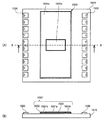
図1は、第1の実施の形態の半導体モジュールを示す図である。
なお、図1(A)は、半導体モジュールの平面図を、図1(B)は、図1(A)の一点鎖線X1−X1の断面図をそれぞれ示している。
FIG. 1 is a diagram illustrating the semiconductor module according to the first embodiment.
1A is a plan view of the semiconductor module, and FIG. 1B is a cross-sectional view taken along one-dot chain line X1-X1 in FIG. 1A.
また、図2〜図10は、第1の実施の形態の半導体モジュールの構成を示す図である。
図2(A)は、ドレイン板1010の平面図を、図2(B)は、図2(A)の一点鎖線X−Xにおける断面図をそれぞれ示している。
2 to 10 are diagrams illustrating the configuration of the semiconductor module according to the first embodiment.
2A is a plan view of the
図3(A)は、ドレイン板1010の平面図を、図3(B)は、図3(A)の矢視Yから見た側面図を、図3(C)は、図3(A)の矢視Xから見た側面図をそれぞれ示している。
3A is a plan view of the
図8(A)は、蓋1300の平面図を、図8(B)は、(ゲート板1400及び補助ソース板1500a,1500bを配置していない)半導体モジュールの斜視図をそれぞれ示している。
8A shows a plan view of the
図9(A)は、ゲート板1400の平面図を、図9(B)は、補助ソース板1500a,1500bの平面図をそれぞれ示している。なお、図10は、図1の一点鎖線X2−X2の断面拡大図を示している。
FIG. 9A shows a plan view of the
非絶縁型の半導体モジュール1000は、図1に示されるように、ドレイン板1010と、半導体素子1020と、積層基板1030と、ゲート端子1040と、補助ソース端子1050と、蓋1300とを備える。また、半導体モジュール1000は、ゲート板1400と、補助ソース端子1060と、補助ソース板1500a,1500bと、絶縁性の枠1200をさらに備えている。
As shown in FIG. 1, the non-insulated
ドレイン板1010は、銅やアルミ等の導電性材料で構成される。ドレイン板1010のおもて面には半導体モジュール1000の各構成部材が搭載され、裏面に外部電源からの電力が入力される。すなわち、ドレイン板1010は、非絶縁型の半導体モジュール1000のドレイン端子としての機能を有する。
The
半導体素子1020は、パワーMOSFET(Metal Oxide Semiconductor Field Effect Transistor)やIGBT等の縦型のパワー半導体素子である。第1の実施の形態においては、半導体素子1020がパワーMOSFETの場合について説明する。半導体素子1020は、おもて面にゲート電極とソース電極とを備え、裏面にドレイン電極を備える。半導体素子1020は、ドレイン板1010のおもて面に配置される。そして、半導体素子1020の裏面のドレイン電極と、ドレイン板1010が、はんだ等の導電性の接合材により接合され、電気的に接続されている。
The
積層基板1030は、図2に示されるように、絶縁板1032と、第1回路板1031aと、第2回路板1031bとを備える。積層基板1030は、ドレイン板1010のおもて面のうち、半導体素子1020が配置されている箇所とは異なる箇所に配置されている。また、第1回路板1031aと半導体素子1020のゲート電極が電気的に接続され、第2回路板1031bと半導体素子1020のソース電極が電気的に接続されている。これらの接続構成の詳細については後述する。
As shown in FIG. 2, the
ゲート端子1040は、第1回路板1031a上に配置されている。一対のソース端子1070,1080は、第2回路板1031b上に配置されている。一対の補助ソース端子1050,1060は、第2回路板1031b上に配置されている。いずれの端子も銅やアルミなどの導電性材料で構成される。また、いずれの端子も第1回路板1031aもしくは第2回路板1031bと、はんだなどの導電性の接合材により接合され、電気的に接続されている。
The
図8に示すように、蓋1300は、矩形状をなし、ガイド溝1303,1304を備える。蓋1300は、ドレイン板1010のおもて面に対向して配置されている。そして、開口1301に、ゲート端子1040、ソース端子1070,1080、及び補助ソース端子1050,1060が位置している。ガイド溝1303,1304は開口1301に接し、開口1301に接する箇所から外周部まで延伸されている。蓋1300は、銅やアルミ等の導電性材料で構成されることが好ましい。
As shown in FIG. 8, the
なお、蓋1300は、ボルト孔1305,1306を用いて、ボルト1073,1083でソース端子1070,1080にねじ止めされ、固定されている。
ゲート板1400は、ガイド溝1303,1304に配置され、ゲート端子1040と電気的に接続され、ガイド溝1303,1304に沿って外周部に延伸されている。なお、ゲート端子1040は、ガイド溝1303,1304の中間点を直交する線上に位置している。
The
The
補助ソース板1500a,1500bは、ガイド溝1303,1304に配置されて、補助ソース端子1050,1060にそれぞれ電気的に接続されている。また、補助ソース板1500a,1500bは、ゲート板1400とは絶縁層1600bにより絶縁されながら、ガイド溝1303,1304に沿って外周部に延伸されている。
The
ゲート板1400は、第1の実施の形態では、H字型の形状をなしており、中心部でゲート端子1040のボルト孔1041にボルト1043で固定されている。補助ソース板1500a,1500bも、補助ソース端子1050及び補助ソース端子1060のボルト孔1051,1061にボルト1053,1063で固定されている。
In the first embodiment, the
このような半導体モジュール1000において、ドレイン板1010にドレイン導体1800を押圧し、ソース端子1070,1080にソース導体1700を押圧して、上下から圧接する。これにより、外部電源と半導体モジュール1000を電気的に接続することができる。また、外周部に延伸され、半導体モジュール1000の側部に取り出されたゲート板1400に、ゲートドライバユニット(不図示)からゲート電圧を印加する。これにより、半導体素子1020のスイッチング動作を制御することができる。
In such a
このような構成を有する半導体モジュールの構成、組み立てについて、以下で説明する。
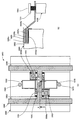
まず、図2に示されるように、ドレイン板1010の中央部に積層基板1030と、積層基板1030の両側に複数の半導体素子1020とがそれぞれ配置されている。
The configuration and assembly of the semiconductor module having such a configuration will be described below.
First, as shown in FIG. 2, a
絶縁板1032のおもて面に、第1回路板1031aと第2回路板1031bとが配置されている。第1回路板1031a及び第2回路板1031bは、銅やアルミ等の導電性材料により構成されている。第1回路板1031aと第2回路板1031bとは、電気的に絶縁されており、第2回路板1031bが第1回路板1031aを取り囲んで配置されている。また、絶縁板1032の裏面に、例えば、銅で構成された金属板1033を備える。金属板1033を配置することにより、ドレイン板1010と積層基板1030との間を、はんだ付けによる接合が可能となる。なお、ドレイン板1010と積層基板1030との間を接着剤で接合する場合は、金属板1033は無くても良い。
A
次いで、図3に示されるように、積層基板1030の第1回路板1031aの中心部に、柱状であって、上面にボルト孔1041が設けられたゲート端子1040が設置される。
Next, as shown in FIG. 3, a
また、第2回路板1031bには、一対のソース端子1070,1080が、第1回路板1031aを挟んで設置される。ソース端子1070,1080には、それぞれ、段差面1072,1082が形成されており、段差面1072,1082には、ボルト孔1071,1081がそれぞれ形成されている。
In addition, a pair of
さらに、第2回路板1031bには、補助ソース端子1050,1060が設置される。補助ソース端子1050,1060は、例えば、第1回路板1031aを挟んで、ソース端子1070,1080と並んで設置される。補助ソース端子1050,1060には、ボルト孔1051,1061がそれぞれ形成されている。なお、図3(A)に示す補助ソース端子1050,1060の設置箇所は、一例であって、第2回路板1031b上であればどこでも構わない。
Further,
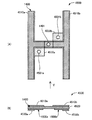
次いで、図4〜図6に示されるように、複数の半導体素子1020と、第1回路板1031a及び第2回路板1031bとの間に、プリント基板1090,1100が設置される。設置の際、プリント基板1090,1100と、補助ソース端子1050,1060が干渉しないように、プリント基板1090,1100の形状が最適化されている。プリント基板1090,1100のおもて面に配置されたゲート配線層1091,1101と、複数の半導体素子1020の各ゲート電極とは、導電ポスト1092a,1102aを経由してそれぞれ電気的に接続されている。また、ゲート配線層1091,1101と、積層基板1030の第1回路板1031aとは、ゲート接続部1095,1105を経由して電気的に接続されている。
Next, as illustrated in FIGS. 4 to 6, printed
また、プリント基板1090,1100の裏面に配置されたソース配線層1093,1103と、複数の半導体素子1020の各ソース電極とは、導電ポスト1092b,1102bを経由してそれぞれ電気的に接続されている。また、ソース配線層1093,1103と、積層基板1030の第2回路板1031bとは、ソース接続部1096,1106を経由して電気的に接続されている。
The
このように、プリント基板1090,1100及び導電ポスト1092a,1092b,1102a,1102bを用いて、半導体素子1020と積層基板1030とが電気的に接続される。
In this manner, the
なお、ソース配線層1093,1103には貫通孔1094,1104が形成されている。プリント基板1090,1100のゲート配線層1091,1101に接続されている導電ポスト1092a,1102aは、貫通孔1094,1104に挿通されている。このため、導電ポスト1092a,1102aとソース配線層1093,1103とは電気的絶縁性が保たれている。
Note that through
このようにして各構成が設置されたドレイン板1010を、図7に示されるように、四方が覆われた枠1200内に設ける。
次いで、枠1200に被せる蓋1300は、図8(A)に示されるように、開口1301と、ボルト孔1305,1306とがそれぞれ形成されている。さらに、蓋1300は、図中上下方向に直線状のガイド溝1303,1304が開口1301に接して、外周部まで延伸されて形成されている。
As shown in FIG. 7, the
Next, as shown in FIG. 8A, the
このような蓋1300を枠1200に被せると、図8(B)に示される半導体モジュール1000となる。半導体モジュール1000では、ゲート端子1040と、ソース端子1070,1080と、補助ソース端子1050,1060とが、開口1301に位置し、開口1301から少なくとも一部が露出するように配置されている。また、ボルト孔1305,1306が、ソース端子1070,1080のボルト孔1071,1081に位置合わせされ、蓋1300がボルト1073,1083で固定されている。
When such a
なお、蓋1300に形成されたガイド溝1303,1304の溝の深さは、例えば、ゲート端子1040と、補助ソース端子1050,1060との高さと一致するようにしている。
Note that the depths of the
次いで、図9及び図10に示されるように、蓋1300のガイド溝1303に、絶縁層1600aを配置して、補助ソース板1500aを配置する。配置の際には、補助ソース板1500aのボルト孔1501aが、補助ソース端子1060のボルト孔1061に位置合わせされ、ボルト1063で固定される。補助ソース板1500bも同様にしてガイド溝1304に絶縁層1600aを介して配置される。この際、補助ソース板1500bのボルト孔1501aが、補助ソース端子1050のボルト孔1051に位置合わせされ、ボルト1053で固定される。
Next, as illustrated in FIGS. 9 and 10, the insulating
また、ガイド溝1303,1304に配置された補助ソース板1500a,1500bに、絶縁層1600bを配置し、図9(A)に示されるゲート板1400を配置する。配置の際には、ゲート板1400のボルト孔1401が、ゲート端子1040のボルト孔1041に位置合わせされ、ボルト1043で固定される。ゲート板1400上にはさらに絶縁層1600cを配置する。
Further, the insulating
すなわち、ガイド溝1303において、図10に示されるように、絶縁層1600a、補助ソース板1500a、絶縁層1600b、ゲート板1400、絶縁層1600cの順で積層される。また、ガイド溝1304において、絶縁層1600a、補助ソース板1500b、絶縁層1600b、ゲート板1400、絶縁層1600cの順で積層される。
That is, in the
このようにして設置された補助ソース板1500a,1500bにゲートドライバユニットを接続すると、ゲートドライバユニットは、ゲート電圧に応じたソース電流を計測することができる。
When the gate driver unit is connected to the
第1の実施の形態の半導体モジュール1000では、蓋1300にガイド溝1303,1304が設けられることにより、ソース端子1070,1080の上面よりも低い位置にゲート板1400を配置することができる。これにより、ゲート板1400とゲート端子1040を接合する、ボルト1043を配置するのに必要なスペースを確保することができる。そして、ボルト1043で強固に接合することにより、動作時におけるゲート端子1040の摩耗の発生が抑制される。このため、ゲート端子1040の電気抵抗の増加、並びに、発熱の発生が抑制されて、半導体モジュール1000の動作不良の発生が防止される。
In the
また、半導体モジュール1000では、補助ソース端子1050,1060を設置して、補助ソース端子1050,1060に接合した補助ソース板1500a,1500bをガイド溝1303,1304から延伸させるようにした。このため、ゲート電圧に対するソース電流を計測することができ、所望のソース電流が出力されるように印加するゲート電圧を正確に制御することができる。
In the
また、ガイド溝1303,1304にゲート板1400及び補助ソース板1500a,1500bを積層配置している。このため、ゲート配線の配線インダクタンスを低減させることができ、半導体モジュールの高速動作が可能となる。
Further, a
また、半導体モジュール1000では、半導体素子1020、積層基板1030等が導電性の蓋1300により覆われているために、半導体モジュール内部で発生するノイズを遮断することができる。
In the
また、半導体モジュール1000は、ゲート板1400と補助ソース板1500a,1500bとがガイド溝1303,1304に収納されるために、コンパクト化される。
なお、第1の実施の形態では、ガイド溝1303,1304に補助ソース板1500a,1500bを先に配置して、ゲート板1400を配置する場合を例に挙げて説明した。この場合に限らず、ゲート板1400を先に配置して、補助ソース板1500a,1500bを配置することも可能である。
Further, the
In the first embodiment, the case where the
また、第1の実施の形態では、半導体素子1020にパワーMOSFETを用いる場合について説明したが、これに限定されるものではなく、半導体素子1020をIGBTにしてもよい。この場合、上記実施の形態におけるドレイン電極はコレクタ電極に、ソース電極はエミッタ電極にそれぞれ置き換えればよい。また、その他のスイッチング素子を用いてもよい。
In the first embodiment, the case where a power MOSFET is used for the
すなわち、第1の出願の明細書及び特許請求の範囲において、「ドレイン電極」とは半導体素子1020の陽極側の電極の総称であり、「ソース電極」とは半導体素子1020の陰極側の電極の総称である。
That is, in the specification and claims of the first application, “drain electrode” is a general term for the anode side electrode of the
[第2の実施の形態]
第2の実施の形態では、第1の実施の形態で示した半導体モジュールを複数組み合わせた半導体装置について、図11及び図12を用いて説明する。
[Second Embodiment]
In the second embodiment, a semiconductor device in which a plurality of semiconductor modules described in the first embodiment are combined will be described with reference to FIGS.
図11は、第2の実施の形態の半導体装置を示す図である。
また、図12は、第2の実施の形態の半導体装置の配線板を示す図である。
図12(A)はゲート板の平面図、図12(B)は補助ソース板の平面図をそれぞれ示している。
FIG. 11 illustrates a semiconductor device according to the second embodiment.
FIG. 12 is a diagram illustrating a wiring board of the semiconductor device according to the second embodiment.
12A is a plan view of the gate plate, and FIG. 12B is a plan view of the auxiliary source plate.
複数(第2の実施の形態では3つ)の半導体モジュール(図8(B))を用意して、ガイド溝1303同士が連結し、またガイド溝1304同士が連結するように配置する。
このようにガイド溝同士を連結した複数の半導体モジュールに対して、図12に示されるような、一体化したゲート板2400と、一体化した補助ソース板2500a,2500bとを用意する。
A plurality of (three in the second embodiment) semiconductor modules (FIG. 8B) are prepared and arranged so that the
As shown in FIG. 12, an
複数を組み合わせた半導体モジュールの連結したガイド溝1303に、絶縁層を介して一体化した補助ソース板2500aを配置する。配置の際には、補助ソース板2500aのボルト孔2501aを、補助ソース端子1060のボルト孔1061に位置合わせする。補助ソース板2500bについても同様に、連結したガイド溝1304に、絶縁層を介して配置する。この際、補助ソース板2500bのボルト孔2501bを、補助ソース端子1050のボルト孔1051に位置合わせする。
An
続いて、第1の実施の形態と同様、補助ソース板2500a,2500bの上に、絶縁層を配置する。
さらに、連結したガイド溝1303,1304の絶縁層を介して、一体化したゲート板2400を配置する。配置の際には、ゲート板2400のボルト孔2401を、ゲート端子1040のボルト孔1041に位置合わせする。
Subsequently, as in the first embodiment, an insulating layer is disposed on the
Further, an
さらに、図11に示されるように、ゲート板2400が、ボルト1043で固定される。また、補助ソース板2500a,2500bが、ボルト1053,1063でそれぞれ固定される。
Furthermore, as shown in FIG. 11, the
このようにして組み合わされた半導体装置100の複数のソース端子1070,1080を、ソース導体(不図示)で押圧する。そして同様に、半導体装置100の複数のドレイン板1010を、ドレイン導体(不図示)で押圧する。これにより、複数の半導体モジュール1000を、容易に並列接続することができる。
The plurality of
このように、第2の実施の形態においては、複数の半導体モジュール1000について、ガイド溝1303,1304が連結するように組み合わせて並列接続した、半導体装置100を構成することができる。これにより、半導体装置100の大電流化を容易に図ることができる。
Thus, in the second embodiment, it is possible to configure the
[第3の実施の形態]
第3の実施の形態では、補助ソース端子を設けずに、補助ソース電流を得ることができる半導体モジュールについて、図13を用いて説明する。
[Third Embodiment]
In the third embodiment, a semiconductor module capable of obtaining an auxiliary source current without providing an auxiliary source terminal will be described with reference to FIG.
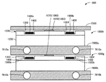
図13は、第3の実施の形態の半導体モジュールを示す図である。
図13(A)は、蓋2300の平面図を、図13(B)は、第3の実施の形態の半導体モジュール2000の平面図をそれぞれ示している。
FIG. 13 is a diagram illustrating a semiconductor module according to the third embodiment.
FIG. 13A shows a plan view of the
半導体モジュール2000では、第1の実施の形態の半導体モジュール1000に示した補助ソース端子1050,1060を配置していない。また、半導体モジュール2000の蓋2300は、図13(A)に示されるように、ソース端子1070,1080と、ゲート端子1040を表出する開口2301が形成されている。さらに、蓋2300は、ガイド溝1303,1304と同じ深さ(高さ)に位置する凹部2302,2303と、凹部2302,2303に設けられたボルト孔2306,2307とを備える。その他は、半導体モジュール1000と同様の構成をなしている。
In the
このような蓋2300を、第1の実施の形態と同様に、半導体素子1020、積層基板1030等を収納する枠1200に被せる。ソース端子1070,1080のボルト孔1071,1081に位置合わせし、ボルト孔1304,1305をボルト1083,1073でねじ止めする。これにより、蓋2300がソース端子1070,1080に固定される。
Similar to the first embodiment, such a
さらに、第1の実施の形態と同様に、補助ソース板1500a,1500bをガイド溝1303,1304に絶縁層を介して配置する。そして、補助ソース板1500a,1500bのボルト孔1501a,1501bを、ボルト孔2307,2306に位置合わせする。そして、補助ソース板1500a,1500bを、ボルト1053,1063でねじ止めして、蓋2300に固定し、電気的に接続する。ゲート板1400も、第1の実施の形態と同様に、ゲート端子1040のボルト孔1041にボルト孔1401を位置合わせし、ボルト1043でねじ止めして、ゲート端子1040に固定される。
Further, as in the first embodiment, the
この際、蓋2300は、ソース端子1070,1080とは電気的に接続されているために、蓋2300とソース端子1070,1080とは同電位となっている。この状態において、補助ソース板1500a,1500bが蓋2300に電気的に接続されているために、補助ソース板1500a,1500bも、ソース端子1070,1080と同電位となる。したがって、第2回路板1031bと、補助ソース板1500a,1500bとの間が、ソース端子1070,1080及び蓋2300を経由して、電気的に接続されている。これにより、第1の実施の形態と同様に、補助ソース板1500a,1500bから補助ソース電流を得ることが可能となる。
At this time, since the
第3の実施の形態により、構成部材の増加を抑えて、補助ソース電流を得ることが可能となる。
[第4の実施の形態]
第4の実施の形態では、半導体モジュールのガイド溝の深さをゲート端子並びに補助ソース端子よりも浅くする場合について、図14を用いて説明する。
According to the third embodiment, it is possible to obtain an auxiliary source current while suppressing an increase in the number of components.
[Fourth Embodiment]
In the fourth embodiment, the case where the depth of the guide groove of the semiconductor module is made shallower than the gate terminal and the auxiliary source terminal will be described with reference to FIG.
図14は、第4の実施の形態の半導体モジュールを示す図である。
図14(A)は、第4の実施の形態の半導体モジュール3000の平面図、図14(B)は、図14(A)の一点鎖線X−Xにおける断面拡大図をそれぞれ示している。
FIG. 14 is a diagram illustrating a semiconductor module according to the fourth embodiment.
FIG. 14A is a plan view of the
半導体モジュール3000は、ガイド溝3303,3304が、第1の実施の形態のガイド溝1303,1304よりも浅く構成されている。なお、半導体モジュール3000の他の構成については、第1の実施の形態の半導体モジュールと同様の構成をなしている。このため、図14(B)に示されるように、ガイド溝3303の底面3303aが、ゲート端子1040の上端部よりも上方に位置しており、ガイド溝3303と、ゲート端子1040の上端部とに段差が生じている。
The
そこで、ガイド溝3303,3304に配置するゲート板1400の中心部には、この段差に応じて傾斜が付けられている。この傾斜により、ゲート板3400のボルト孔がゲート端子1040のボルト孔1041に位置合わせされ、ゲート板3400がゲート端子1040にボルト1043で固定される。
Therefore, the central portion of the
また、補助ソース板3500a,3500bも、図示を省略するものの、ボルト孔が形成されている箇所に、ゲート板3400と同様に傾斜が付けられている。
これにより、ゲート板3400と補助ソース板3500a,3500bとが配置されるガイド溝3303,3304の隙間(空間)を小さくすることができる。このために、半導体モジュール3000の低インダクタンス化を図ることができる。したがって、ガイド溝3303,3304の深さは、隙間が最も少ない、ゲート板3400と、補助ソース板3500a,3500bと、絶縁層とを合わせた厚さ程度とすることが望ましい。
In addition, the
As a result, the gap (space) between the
また、半導体モジュール3000は、第2の実施の形態の半導体モジュール(図11)と同様に、ガイド溝3303,3304が連結するように複数組み合わせることも可能である。
Further, as in the semiconductor module of the second embodiment (FIG. 11), a plurality of
[第5の実施の形態]
第5の実施の形態では、第1の実施の形態のゲート板1400と補助ソース板1500a,1500bとをプリント基板にして一体化した場合について、図15を用いて説明する。
[Fifth Embodiment]
In the fifth embodiment, a case where the
図15は、第5の実施の形態の半導体モジュールに用いられるゲート板と補助ソース板とを含むプリント基板を示す図である。
図15(A)は、ゲート板1400と補助ソース板1500a,1500bとを含むプリント基板の平面図を、図15(B)は、図15(A)の矢視Yから見た側面図をそれぞれ示している。
FIG. 15 is a diagram illustrating a printed circuit board including a gate plate and an auxiliary source plate used in the semiconductor module according to the fifth embodiment.
15A is a plan view of a printed circuit board including the
プリント基板4500は、第1の実施の形態のゲート板1400と、補助ソース板1500a,1500bとの間に絶縁材料で構成された基材4520が挟まれている。ゲート板1400上にはレジスト層4510a,4510bが形成され、またボルト孔1041部分が開口されている。また、補助ソース板1500a,1500bには、レジスト層4510a,4510bが形成され、ボルト孔1501a,1501bに対向する開口4531a,4531bが形成されている。
In the printed
そして、第1の実施の形態の半導体モジュール1000の開口1301、ガイド溝1303,1304にプリント基板4500が嵌めこまれて、ボルト1043,1053,1063で固定される。
Then, the printed
このようなプリント基板4500を用いることにより、ゲート板1400と、補助ソース板1500a,1500bの取り付けが容易になる。
なお、複数の半導体モジュールを組み合わせる場合には、例えば、第4の実施の形態に示したゲート板2400と、補助ソース板2500a,2500bとを、プリント基板として一体化することが可能である。
By using such a printed
When a plurality of semiconductor modules are combined, for example, the
[第6の実施の形態]
第6の実施の形態では半導体モジュールを6つ組み合わせた場合について、図16を用いて説明する。
[Sixth Embodiment]
In the sixth embodiment, a case where six semiconductor modules are combined will be described with reference to FIG.
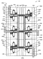
図16は、第6の実施の形態の半導体装置を示す図である。
半導体モジュール1000a〜1000fは、半導体モジュール1000と同様の構成をなしている。但し、半導体モジュール1000a〜1000fの蓋4300には、ガイド溝1303,1304の中心部から外周部に通じるガイド溝1308,1309がさらに形成されている。なお、図16では、半導体モジュール1000aにのみ符号を付しており、半導体モジュール1000b〜1000fに対する符号は省略している。
FIG. 16 illustrates a semiconductor device according to the sixth embodiment.
The
このような半導体モジュール1000a〜1000fを、図16のように縦3つ、横2つ並列に配置させている。
そして、ゲート板5400aが半導体モジュール1000aのガイド溝1303に配置され、半導体モジュール1000aのゲート端子1040にボルト1043で固定されている。
The
ゲート板5500aは、半導体モジュール1000aのガイド溝1304と、半導体モジュール1000bのガイド溝1304,1308とに配置され、半導体モジュール1000bのゲート端子1040にボルト1043で固定されている。
The
ゲート板5600aは、半導体モジュール1000bのガイド溝1304と、半導体モジュール1000cのガイド溝1304とに配置され、半導体モジュール1000cのゲート端子1040にボルト1043で固定されている。
The
また、ゲート板5600bは、半導体モジュール1000dのガイド溝1303と、半導体モジュール1000eのガイド溝1303とに配置され、半導体モジュール1000dのゲート端子1040にボルト1043で固定されている。
The
ゲート板5500bは、半導体モジュール1000eのガイド溝1303,1309と、半導体モジュール1000fのガイド溝1303とに配置され、半導体モジュール1000eのゲート端子1040にボルト1043で固定されている。
The
ゲート板5400bは、半導体モジュール1000fのガイド溝1304に配置され、半導体モジュール1000fのゲート端子1040にボルト1043で固定されている。
接続板5700aが、半導体モジュール1000aのガイド溝1309と半導体モジュール1000dのガイド溝1308とに配置されている。接続板5700aと、ゲート板5400a,5500aとが、ボルト5801で固定され、接続板5700aと、ゲート板5600bとが、ボルト5804で固定されている。
The
The
接続板5700bが、半導体モジュール1000bのガイド溝1309と半導体モジュール1000eのガイド溝1308とに配置されている。接続板5700bと、ゲート板5500a,5600aとが、ボルト5802で固定され、接続板5700bと、ゲート板5600b,5500bとが、ボルト5805で固定されている。
The
接続板5700cが、半導体モジュール1000cのガイド溝1309と半導体モジュール1000fのガイド溝1308とに配置されている。接続板5700cと、ゲート板5600aとが、ボルト5803で固定され、接続板5700cとゲート板5500b,5400bとが、ボルト5806で固定されている。
The
このようにして複数の半導体モジュール1000a〜1000fが組み合わされた半導体装置200では、裏面のドレイン板1010からドレイン電圧が印加される。そして、ゲートドライバユニットからゲート板5400a,5500a,5500b,5400bにそれぞれゲート電圧が印加されると、各ソース端子1070,1080からソース電流が出力される。
In the
このように、半導体モジュールの蓋4300に、外周部に通じるガイド溝1308,1309を配置することにより、複数の半導体モジュールの配置パターン数を増加することができる。これにより、より柔軟に半導体装置200の大電流化を図ることができる。
As described above, by arranging the
[第7の実施の形態]
第7の実施の形態では、第1の実施の形態の半導体モジュール1000において、補助ソース板が配置されるガイド溝を新たに設けた場合について説明する。
[Seventh Embodiment]
In the seventh embodiment, a case where a guide groove in which the auxiliary source plate is disposed is newly provided in the
図17は、第7の実施の形態の半導体モジュールを示す図である。
半導体モジュール5000では、蓋5300以外については、半導体モジュール1000と同様の構成がなされている。
FIG. 17 illustrates a semiconductor module according to the seventh embodiment.
The
蓋5300は、ゲート端子1040と隣接し、開口1301に接して形成されたガイド溝5303を備える。さらに、当該ガイド溝5303と平行に配置され、ボルト孔5305a,5305bを備えるガイド溝5304が形成されている。そして、ガイド溝5304に沿って、図示しない補助ソース板が配置され、補助ソース板はボルト孔5305a,5305bを用いて固定される。
The
また、蓋5300は、ソース端子1070,1080にボルト1073,1083で固定されている。このため、蓋5300は、ソース端子1070,1080と同電位である。したがって、第2回路板1031bと、補助ソース板とを同電位にすることが可能となる。
The
なお、ゲート板が配置されるガイド溝5303は、図17の形成位置に限らず、第1の実施の形態と同様に、開口5301の両側に形成することも、または、開口5301の図中左側のみに形成することも可能である。
Note that the
また、半導体モジュール5000を複数組み合わせた場合について、図18を用いて説明する。
図18は、第7の実施の形態の半導体モジュールを複数組み合わせた半導体装置を示す図である。
A case where a plurality of
FIG. 18 is a diagram illustrating a semiconductor device in which a plurality of semiconductor modules according to the seventh embodiment are combined.
複数(第7の実施の形態では3つ)の半導体モジュール5000を用意して、ガイド溝5303,5304がそれぞれ連結するように配置する。
連結したガイド溝5303に絶縁層を介して、ゲート板5400を配置して、ゲート板5400をゲート端子1040にボルト1043で固定する。
A plurality (three in the seventh embodiment) of
A
同様にして、連結したガイド溝5304に絶縁層を介して、補助ソース板5500を配置して、補助ソース板5500をガイド溝5304にボルト5503a,5503bで固定する。
Similarly, the
このようにして複数の半導体モジュール5000を組み合わせた半導体装置300では、各半導体モジュール5000から出力されるソース電流が合成されて、半導体装置の大電流化を図ることができる。
In the
[第8の実施の形態]
第8の実施の形態では、第7の実施の形態の半導体モジュール5000において、補助ソース板が配置されるガイド溝を別の箇所に設けた場合について説明する。
[Eighth Embodiment]
In the eighth embodiment, a case where a guide groove in which the auxiliary source plate is arranged is provided in another location in the
図19は、第8の実施の形態の半導体モジュールを示す図である。
図19(A)は、蓋6300が設置された半導体モジュール6000の平面図、図19(B)は、半導体モジュール6000の内部平面図をそれぞれ示している。
FIG. 19 is a diagram illustrating a semiconductor module according to the eighth embodiment.
19A is a plan view of the
半導体モジュール6000は、蓋6300及び補助ソース端子6060以外については、半導体モジュール1000と同様の構成がなされている。
蓋6300は、ゲート端子1040と隣接し、開口6301に接して形成されたガイド溝6303を備える。さらに、開口6301の図中左側に、ガイド溝6303と平行に配置され、ボルト孔6305aを備える補助ガイド溝6304が形成されている。
The
The
補助ソース端子6060は、第2回路板1031b上に配置されている。蓋6300が枠1200に設置されると、補助ガイド溝6304のボルト孔6305aと、補助ソース端子6060のボルト孔6061とが位置合わせされる。
The
そして、補助ガイド溝6304に沿って、図示しない補助ソース板が絶縁層を介して配置され、ボルト孔6305aを用いて図示しないボルトにより固定される。
また、このような半導体モジュール6000を複数組み合わせた半導体装置400について、図20を用いて説明する。
Then, an auxiliary source plate (not shown) is disposed along the
A
図20は、第8の実施の形態の半導体モジュールを複数組み合わせた半導体装置を示す図である。
複数(第8の実施の形態では3つ)の半導体モジュール6000を用意して、ガイド溝6303と補助ガイド溝6304が連結するように配置する。
FIG. 20 is a diagram illustrating a semiconductor device in which a plurality of semiconductor modules according to the eighth embodiment are combined.
A plurality (three in the eighth embodiment) of
そして、連結したガイド溝6303に絶縁層を介してゲート板6400を配置して、ゲート板6400をゲート端子1040にボルト1043で固定する。
同様にして、連結した補助ガイド溝6304に絶縁層を介して、補助ソース板6500を配置して、補助ソース板6500を補助ガイド溝6304のボルト孔6305aに、ボルト6503でねじ止めして固定する。
Then, the
Similarly, the
このようにして半導体モジュール6000が組み合わされた半導体装置400では、各半導体モジュール6000から出力されるソース電流が合成されて、半導体装置400の大電流化を図ることができる。
In the
[第9の実施の形態]
第9の実施の形態では、半導体モジュール1000を直列に組み合わせた場合について図21及び図22を用いて説明する。
[Ninth Embodiment]
In the ninth embodiment, a case where the
図21及び図22は、第9の実施の形態の半導体装置を示す側面図である。
なお、図21では、複数の半導体モジュールを縦方向に配列して、図22は、複数の半導体モジュールを横方向に配列して、それぞれ直列に組み合わせた半導体装置を示す側面図である。
21 and 22 are side views showing the semiconductor device according to the ninth embodiment.
In FIG. 21, a plurality of semiconductor modules are arranged in the vertical direction, and FIG. 22 is a side view showing a semiconductor device in which a plurality of semiconductor modules are arranged in the horizontal direction and combined in series.
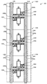
図21に示すように、金属製の冷却フィン7600bに、第1の実施の形態の半導体モジュール1000gを載置して、半導体モジュール1000gのドレイン板1010と冷却フィン7600bとを電気的に接続させる。当該半導体モジュール1000g上に冷却フィン7600aを載置して、半導体モジュール1000gのソース端子1070,1080と冷却フィン7600aとを電気的に接続させる。
As shown in FIG. 21, the
冷却フィン7600aに、さらに、半導体モジュール1000hを載置して、半導体モジュール1000hのドレイン板1010と冷却フィン7600aとを電気的に接続させる。半導体モジュール1000hのソース端子1070,1080に、ソース板7500を圧接させる。
Further, the
なお、冷却フィン7600a,7600bには、水が流れるパイプ7610a,7610bが内部に形成されている。冷却フィン7600a,7600bはパイプ7610a,7610bに水が流れることで、半導体モジュール1000h,1000gをより効果的に冷却することができる。
Note that
このように半導体モジュール1000h,1000gを積層させて組み合わせた半導体装置500は、冷却フィン7600bからドレイン電圧を印加して、各半導体モジュール1000g,1000hのゲート板1400にゲートユニットドライバからゲート電圧を印加する。すると、半導体モジュール1000g、冷却フィン7600a、及び半導体モジュール1000hを経由して出力したソース電流がソース板7500から得られる。すなわち、第9の実施の形態の半導体装置500の定格電圧は、半導体モジュール1000の定格電圧の2倍となる。
In this way, the
なお、第9の実施の形態において、半導体モジュール1000h,1000gは2つ、すなわち2段に限られず、3段以上であっても積層して直列接続することが可能である。また、第2,第6の実施の形態のように並列に組み合わせた半導体モジュール1000を、さらに任意の段数直列に設置することも可能である。例えば、直列に3段積層させる場合であって、ドレイン板1010からソース端子1070,1080に順に半導体モジュール1000を1段目に2並列、2段目に4並列、3段目に3並列、合計9つの半導体モジュール1000を設置することができる。この際の半導体装置の定格電圧、定格電流は9つの半導体モジュール1000で一致する必要はない。定格電圧が一致しない場合、半導体装置の定格電圧は、各段における定格電圧が最低である半導体モジュール1000の3つの和に等しい。また、定格電流が一致しない場合、半導体装置の定格電流は、各段の3つの定格電流のうち、最低となる段の定格電流に等しい。
In the ninth embodiment, the
また、冷却フィン7600a,7600bに限らず、導電部材を介して積層することや、半導体モジュール1000h,1000g同士を直接積層することも可能である。
次いで、複数の半導体モジュール1000を直列に接続するに当たって、半導体モジュール1000を横方向に配置する場合について、図22を用いて説明する。
Moreover, it is not limited to the
Next, when connecting a plurality of
半導体装置600は、図22に示されるように、冷却フィン7600a,7600bを並列に配置し、冷却フィン7600aに半導体モジュール1000hを配置し、冷却フィン7600bに半導体モジュール1000gを配置する。半導体モジュール1000hのドレイン板と接続された冷却フィン7600aと、半導体モジュール1000gのソース端子1070,1080とを、金属プレート7700で圧接して電気的に接続する。但し、冷却フィン7600a,7600bと金属プレート7700との間には絶縁層7800a,7800bを挟んで電気的に絶縁している。
As shown in FIG. 22, in the
このようにして半導体モジュール1000を横方向に配列して、直列接続することが可能である。
In this way, the
100 半導体装置
1000 半導体モジュール
1010 ドレイン板
1020 半導体素子
1030 積層基板
1031a 第1回路板
1031b 第2回路板
1032 絶縁板
1033 金属板
1040 ゲート端子
1041,1051,1061,1071,1081,1305,1306,1401,1501a,1501b ボルト孔
1043,1053,1063,1073,1083 ボルト
1050,1060 補助ソース端子
1070,1080 ソース端子
1072,1082 段差面
1090,1100 プリント基板
1091,1101 ゲート配線層
1093,1103 ソース配線層
1092a,1092b,1102a,1102b 導電ポスト
1094,1104 貫通孔
1095,1105 ゲート接続部
1096,1106 ソース接続部
1200 枠
1300 蓋
1301 開口
1303,1304 ガイド溝
1400 ゲート板
1500a,1500b 補助ソース板
1600a,1600b,1600c 絶縁層
1700 ソース導体
1800 ドレイン導体
DESCRIPTION OF
Claims (14)
おもて面にゲート電極とソース電極とを備え、裏面にドレイン電極を備え、前記ドレイン板のおもて面に配置され、前記ドレイン電極と前記ドレイン板とが電気的に接続される、半導体素子と、
絶縁板と、前記絶縁板のおもて面に設けられた第1回路板及び第2回路板とを備え、前記ドレイン板のおもて面に配置され、前記第1回路板は前記ゲート電極と電気的に接続され、前記第2回路板は前記ソース電極と電気的に接続された、積層基板と、
前記第1回路板上に配置されたゲート端子と、
前記第2回路板上に配置されたソース端子と、
開口及びガイド溝を備え、前記ドレイン板のおもて面と対向して配置され、前記ゲート端子及び前記ソース端子が前記開口に位置し、前記ガイド溝は前記開口に接して外周部まで延伸されている、蓋と、
を備える半導体モジュール。 A drain plate;
A semiconductor comprising a gate electrode and a source electrode on the front surface, a drain electrode on the back surface, disposed on the front surface of the drain plate, and electrically connecting the drain electrode and the drain plate. Elements,
An insulating plate; and a first circuit plate and a second circuit plate provided on a front surface of the insulating plate, and disposed on a front surface of the drain plate, wherein the first circuit plate is the gate electrode. A laminated substrate, wherein the second circuit board is electrically connected to the source electrode;
A gate terminal disposed on the first circuit board;
A source terminal disposed on the second circuit board;
An opening and a guide groove are provided to be opposed to the front surface of the drain plate, the gate terminal and the source terminal are located in the opening, and the guide groove is in contact with the opening and extended to an outer peripheral portion. The lid,
A semiconductor module comprising:
をさらに有する請求項1記載の半導体モジュール。 A gate plate electrically connected to the gate terminal and extended to the outer periphery along the guide groove;
The semiconductor module according to claim 1, further comprising:
前記補助ソース端子と電気的に接続され、前記ガイド溝に沿って前記ゲート板とは電気的に絶縁されて外周部に延伸された補助ソース板と、
をさらに有する請求項2記載の半導体モジュール。 An auxiliary source terminal disposed on the second circuit board and positioned in the opening;
An auxiliary source plate electrically connected to the auxiliary source terminal, electrically insulated from the gate plate along the guide groove, and extended to the outer periphery; and
The semiconductor module according to claim 2, further comprising:
前記補助ガイド溝に沿って外周部に延伸された補助ソース板と、
をさらに有し、
前記ガイド溝は前記開口の一方に接して形成され、
前記補助ガイド溝は前記開口の他方に接して形成され、
前記第2回路板と前記補助ソース板との間が、前記ソース端子及び前記蓋を経由して電気的に接続されている、
請求項2記載の半導体モジュール。 An auxiliary guide groove provided in the lid;
An auxiliary source plate extended to the outer periphery along the auxiliary guide groove;
Further comprising
The guide groove is formed in contact with one of the openings,
The auxiliary guide groove is formed in contact with the other of the openings,
Between the second circuit board and the auxiliary source plate is electrically connected via the source terminal and the lid,
The semiconductor module according to claim 2.
前記ゲート端子と、一対の前記ソース端子とは前記ガイド溝と平行に直線状に配置されている請求項6記載の半導体モジュール。 A pair of source terminals are provided on the second circuit board;
The semiconductor module according to claim 6, wherein the gate terminal and the pair of source terminals are linearly arranged in parallel with the guide groove.
請求項1から4のいずれか1項に記載の半導体モジュール。 The bottom of the guide groove is located above the upper end of the gate terminal;
The semiconductor module of any one of Claim 1 to 4.
複数の前記半導体モジュールは、前記ガイド溝同士が連結されるように配置され、
当該連結された前記ガイド溝に沿って、一体化された前記ゲート板が配置されている、
半導体装置。 A plurality of the semiconductor modules according to claim 2,
The plurality of semiconductor modules are arranged so that the guide grooves are connected to each other,
The integrated gate plate is disposed along the connected guide grooves.
Semiconductor device.
複数の前記半導体モジュールは、前記ガイド溝同士が連結されるように配置され、
当該連結された前記ガイド溝に沿って、一体化された前記ゲート板及び一体化された前記補助ソース板が配置されている、
半導体装置。 A plurality of the semiconductor modules according to claim 3,
The plurality of semiconductor modules are arranged so that the guide grooves are connected to each other,
The integrated gate plate and the integrated auxiliary source plate are disposed along the connected guide grooves.
Semiconductor device.
複数の前記半導体モジュールは、前記ガイド溝同士が連結されるように配置され、前記補助ガイド溝同士が連結されるように配置され、
当該連結された前記ガイド溝に沿って一体化された前記ゲート板が配置され、
当該連結された前記補助ガイド溝に沿って一体化された前記補助ソース板が配置されている、
半導体装置。 A plurality of the semiconductor modules according to claim 4,
The plurality of semiconductor modules are arranged so that the guide grooves are connected to each other, and the auxiliary guide grooves are connected to each other,
The gate plate integrated along the connected guide groove is disposed,
The auxiliary source plate integrated along the connected auxiliary guide groove is disposed,
Semiconductor device.
複数の前記半導体モジュールは、前記半導体モジュールの前記ソース端子と、別の前記半導体モジュールの前記ドレイン板とが電気的に接続されている、
半導体装置。 A plurality of the semiconductor modules according to claim 1,
In the plurality of semiconductor modules, the source terminal of the semiconductor module and the drain plate of another semiconductor module are electrically connected.
Semiconductor device.
前記半導体モジュールの前記ソース端子と、隣接する前記半導体モジュールの前記ドレイン板が電気的に接続されている、
請求項12記載の半導体装置。 A plurality of the semiconductor modules are stacked and arranged,
The source terminal of the semiconductor module and the drain plate of the adjacent semiconductor module are electrically connected;
The semiconductor device according to claim 12.
前記半導体モジュールの前記ソース端子と、隣接する前記半導体モジュールの前記ドレイン板が導電部材を経由して電気的に接続されている、
請求項12記載の半導体装置。 A plurality of the semiconductor modules are arranged side by side,
The source terminal of the semiconductor module and the drain plate of the adjacent semiconductor module are electrically connected via a conductive member;
The semiconductor device according to claim 12.
Priority Applications (4)
| Application Number | Priority Date | Filing Date | Title |
|---|---|---|---|
| JP2015075251A JP6439552B2 (en) | 2015-04-01 | 2015-04-01 | Semiconductor module and semiconductor device |
| CN201610130201.2A CN106057740B (en) | 2015-04-01 | 2016-03-08 | Semiconductor module and semiconductor device |
| DE102016203819.2A DE102016203819B4 (en) | 2015-04-01 | 2016-03-09 | Semiconductor module and semiconductor device |
| US15/069,404 US9524919B2 (en) | 2015-04-01 | 2016-03-14 | Semiconductor module and semiconductor device |
Applications Claiming Priority (1)
| Application Number | Priority Date | Filing Date | Title |
|---|---|---|---|
| JP2015075251A JP6439552B2 (en) | 2015-04-01 | 2015-04-01 | Semiconductor module and semiconductor device |
Publications (2)
| Publication Number | Publication Date |
|---|---|
| JP2016195216A JP2016195216A (en) | 2016-11-17 |
| JP6439552B2 true JP6439552B2 (en) | 2018-12-19 |
Family
ID=56937228
Family Applications (1)
| Application Number | Title | Priority Date | Filing Date |
|---|---|---|---|
| JP2015075251A Expired - Fee Related JP6439552B2 (en) | 2015-04-01 | 2015-04-01 | Semiconductor module and semiconductor device |
Country Status (4)
| Country | Link |
|---|---|
| US (1) | US9524919B2 (en) |
| JP (1) | JP6439552B2 (en) |
| CN (1) | CN106057740B (en) |
| DE (1) | DE102016203819B4 (en) |
Families Citing this family (1)
| Publication number | Priority date | Publication date | Assignee | Title |
|---|---|---|---|---|
| JP7545298B2 (en) * | 2020-11-13 | 2024-09-04 | 株式会社日立製作所 | Power Conversion Equipment |
Family Cites Families (12)
| Publication number | Priority date | Publication date | Assignee | Title |
|---|---|---|---|---|
| GB930704A (en) * | 1960-09-05 | 1963-07-10 | Sony Corp | A balanced esaki diode pair |
| JPS62142856U (en) * | 1986-02-28 | 1987-09-09 | ||
| JPH0666411B2 (en) * | 1987-11-06 | 1994-08-24 | 富士電機株式会社 | Flat semiconductor device |
| JPH0734457B2 (en) * | 1988-04-05 | 1995-04-12 | 株式会社東芝 | Semiconductor device |
| JPH0312410A (en) | 1989-06-08 | 1991-01-21 | Mitsui Petrochem Ind Ltd | Fluorine-containing copolymer and contact lens made thereof |
| JP2882143B2 (en) * | 1991-12-10 | 1999-04-12 | 富士電機株式会社 | Internal wiring structure of semiconductor device |
| JP3228043B2 (en) | 1994-03-24 | 2001-11-12 | 富士電機株式会社 | Parallel connection structure of flat semiconductor switches |
| EP0674380B1 (en) * | 1994-03-24 | 1999-05-06 | Fuji Electric Co. Ltd. | Parallel connection structure for flat type semiconductor switches |
| JP3228021B2 (en) | 1994-09-13 | 2001-11-12 | 富士電機株式会社 | Inverter unit and inverter device |
| DE102004044619B4 (en) * | 2004-09-13 | 2009-07-16 | Infineon Technologies Ag | Capacitor structure in trench structures of semiconductor devices and semiconductor devices with such capacitor structures and method for making the same |
| JP5338830B2 (en) * | 2011-03-15 | 2013-11-13 | 株式会社豊田自動織機 | Semiconductor device |
| JP6330436B2 (en) * | 2014-04-01 | 2018-05-30 | 富士電機株式会社 | Power semiconductor module |
-
2015
- 2015-04-01 JP JP2015075251A patent/JP6439552B2/en not_active Expired - Fee Related
-
2016
- 2016-03-08 CN CN201610130201.2A patent/CN106057740B/en not_active Expired - Fee Related
- 2016-03-09 DE DE102016203819.2A patent/DE102016203819B4/en not_active Expired - Fee Related
- 2016-03-14 US US15/069,404 patent/US9524919B2/en active Active
Also Published As
| Publication number | Publication date |
|---|---|
| CN106057740A (en) | 2016-10-26 |
| US20160293517A1 (en) | 2016-10-06 |
| US9524919B2 (en) | 2016-12-20 |
| JP2016195216A (en) | 2016-11-17 |
| CN106057740B (en) | 2019-12-10 |
| DE102016203819B4 (en) | 2021-03-18 |
| DE102016203819A1 (en) | 2016-10-06 |
Similar Documents
| Publication | Publication Date | Title |
|---|---|---|
| KR101926854B1 (en) | Semiconductor device | |
| US8686601B2 (en) | Power conversion apparatus for vehicle use | |
| EP3107120B1 (en) | Power semiconductor module | |
| JP5434986B2 (en) | Semiconductor module and semiconductor device including the same | |
| US20100328833A1 (en) | Power module with additional transient current path and power module system | |
| JP7519356B2 (en) | Semiconductor Device | |
| CN108400716B (en) | Low inductance half-bridge device | |
| TWI716075B (en) | Power module | |
| US20160255714A1 (en) | Power converter | |
| WO2016129097A1 (en) | Half-bridge power semiconductor module, and method for manufacturing same | |
| JP4660214B2 (en) | Power semiconductor device | |
| CN104218829A (en) | Inverted unit | |
| KR20150036347A (en) | Semiconductor device | |
| CN110875265A (en) | Semiconductor device and power converter | |
| CN109994441B (en) | Electronic components with enhanced high power density | |
| JP4356434B2 (en) | 3-level inverter circuit | |
| JP6922450B2 (en) | Semiconductor module | |
| JP6439552B2 (en) | Semiconductor module and semiconductor device | |
| JP4349364B2 (en) | Semiconductor device | |
| JP3741002B2 (en) | Mounting structure of semiconductor device | |
| JP6979997B2 (en) | Power semiconductor devices | |
| JP2017184376A (en) | Power converter | |
| CN112652612A (en) | Stacked crimping type power module and manufacturing method thereof | |
| JP7533740B2 (en) | Power Conversion Equipment | |
| JP7215402B2 (en) | semiconductor equipment |
Legal Events
| Date | Code | Title | Description |
|---|---|---|---|
| A621 | Written request for application examination |
Free format text: JAPANESE INTERMEDIATE CODE: A621 Effective date: 20180214 |
|
| A977 | Report on retrieval |
Free format text: JAPANESE INTERMEDIATE CODE: A971007 Effective date: 20181004 |
|
| TRDD | Decision of grant or rejection written | ||
| A01 | Written decision to grant a patent or to grant a registration (utility model) |
Free format text: JAPANESE INTERMEDIATE CODE: A01 Effective date: 20181023 |
|
| A61 | First payment of annual fees (during grant procedure) |
Free format text: JAPANESE INTERMEDIATE CODE: A61 Effective date: 20181105 |
|
| R150 | Certificate of patent or registration of utility model |
Ref document number: 6439552 Country of ref document: JP Free format text: JAPANESE INTERMEDIATE CODE: R150 |
|
| R250 | Receipt of annual fees |
Free format text: JAPANESE INTERMEDIATE CODE: R250 |
|
| R250 | Receipt of annual fees |
Free format text: JAPANESE INTERMEDIATE CODE: R250 |
|
| R250 | Receipt of annual fees |
Free format text: JAPANESE INTERMEDIATE CODE: R250 |
|
| LAPS | Cancellation because of no payment of annual fees |