JP6439384B2 - Coil parts - Google Patents
Coil parts Download PDFInfo
- Publication number
- JP6439384B2 JP6439384B2 JP2014222717A JP2014222717A JP6439384B2 JP 6439384 B2 JP6439384 B2 JP 6439384B2 JP 2014222717 A JP2014222717 A JP 2014222717A JP 2014222717 A JP2014222717 A JP 2014222717A JP 6439384 B2 JP6439384 B2 JP 6439384B2
- Authority
- JP
- Japan
- Prior art keywords
- coil
- wiring pattern
- coil core
- wiring patterns
- plan
- Prior art date
- Legal status (The legal status is an assumption and is not a legal conclusion. Google has not performed a legal analysis and makes no representation as to the accuracy of the status listed.)
- Active
Links
Images


Description
本発明は、コイルコアが埋設された絶縁層と、コイルコアの周囲に巻回されたコイル電極とを備えるコイル部品に関する。 The present invention relates to a coil component including an insulating layer in which a coil core is embedded and a coil electrode wound around the coil core.
高周波信号が用いられる電子機器では、ノイズを防止するためにコイル部品が使用される場合がある。この種のコイル部品では、磁性体材料などで形成されたコイルコアと、コイルコアを巻回するコイル電極で構成される場合がある。ここで、コイル電極の巻回は手作業により行われる場合が多く、この手作業をなくすことがコイル部品の製造コストの低減を図る上での課題となっていた。 In an electronic device using a high-frequency signal, a coil component may be used to prevent noise. This type of coil component may be composed of a coil core formed of a magnetic material or the like and a coil electrode around which the coil core is wound. Here, the winding of the coil electrode is often performed manually, and eliminating this manual operation has been an issue in reducing the manufacturing cost of the coil component.
そこで、従来では、コイル電極の巻回に手作業を不要にしたコイル部品が提案されている。例えば、図10に示す特許文献1に記載のコイル部品100は、配線基板101と、配線基板101の一方主面に載置された環状のコイルコア102と、コイルコア102の周囲を巻回するコイル電極103とを備える。
Therefore, conventionally, a coil component has been proposed that does not require manual work for winding the coil electrode. For example, a
このコイル電極103は、配線基板101の上面に形成された複数の配線膜104と、コイルコア102の外側面、上面および内側面を囲むように略コ字状に形成された複数の上側配線子105とで構成される。ここで、各配線膜104には、その両端部それぞれに一の上側配線子105の先端を挿入するための挿入孔が設けられ、これらの挿入孔に上側配線子105の先端を挿入して半田で固定することで、コイルコア102の周囲を螺旋状に巻回するコイル電極103が形成される。この構成によると、1本の線材をコイルコア102に巻回することなくコイル電極103を形成することができるため、コイル部品100の自動化を図ることができる。
The coil electrode 103 includes a plurality of
ところで、この種のコイル部品では、コイル部品のサイズを大きくせずに、コイル特性を向上させることが要求されている。コイル特性の向上を図る例としては、コイル電極の巻数を増やして、高いインダクタンスを得ることが考えられる。しかしながら、従来のコイル電極103では、各上側配線子105のコイルコア102の上側を通る上側配線部105aは、それぞれ平面視でコイルコア102(コイルコア102のコイル電極103の巻回方向に平行な中心軸)に直交するように配置されているが、各配線膜104は、それぞれ平面視でコイルコア102に対して斜めに配置される。このように、平面視で、各上側配線部105aと各配線膜104の方向が異なり、斜めに配置されると、コイル電極103の巻数を増やすのが困難になる。
By the way, this type of coil component is required to improve the coil characteristics without increasing the size of the coil component. As an example of improving the coil characteristics, it is conceivable to increase the number of turns of the coil electrode to obtain a high inductance. However, in the conventional coil electrode 103, the upper wiring portion 105 a passing through the upper side of the
本発明は、上記した課題に鑑みてなされたものであり、コイルコアを巻回するコイル電極の巻数を容易に増やすことができるコイル部品を提供することを目的とする。 The present invention has been made in view of the above-described problems, and an object thereof is to provide a coil component that can easily increase the number of turns of a coil electrode that winds a coil core.
上記した目的を達成するために、本発明のコイル部品は、コイルコアが埋設された絶縁層と、前記コイルコアの周囲に巻回されたコイル電極とを備え、前記コイル電極は、一端が前記コイルコアの一方側に配置されるとともに他端が前記コイルコアの他方側に配置され、前記絶縁層の一方主面に配列された複数の第1配線パターンと、一端が前記コイルコアの一方側に配置されるとともに他端が前記コイルコアの他方側に配置され、前記各第1配線パターンそれぞれと複数の対を成すように前記絶縁層の他方主面に配列された複数の第2配線パターンと、前記コイルコアの前記一方側に配置され、前記各第1配線パターンそれぞれの一端と、当該第1配線パターンと対を成す前記第2配線パターンの一端とを接続する複数の一方側導体と、前記コイルコアの前記他方側に配置され、前記各第1配線パターンそれぞれの他端と、当該第1配線パターンと対を成す前記第2配線パターンに隣接する前記第2配線パターンの他端とを接続する複数の他方側導体とを有し、前記各第1配線パターンおよび前記各第2配線パターンが、前記コイルコアの前記コイル電極の巻回軸方向と平行な中心軸に平面視で直交するように配置され、前記各一方側導体および前記各他方側導体は、対を成す前記第1配線パターンと前記第2配線パターンとの平面視での間隔に等しい幅を有して、前記第1配線パターンとの接触位置と、前記第2配線パターンとの接触位置とが平面視でずれて配置されていることを特徴としている。 In order to achieve the above object, a coil component of the present invention includes an insulating layer in which a coil core is embedded, and a coil electrode wound around the coil core, and the coil electrode has one end of the coil core. A plurality of first wiring patterns arranged on one side and the other end arranged on the other side of the coil core, arranged on one main surface of the insulating layer, and one end arranged on one side of the coil core The other end of the coil core is disposed on the other side of the coil core, and a plurality of second wiring patterns arranged on the other main surface of the insulating layer so as to form a plurality of pairs with the first wiring patterns. A plurality of one-side conductors arranged on one side and connecting one end of each of the first wiring patterns and one end of the second wiring pattern paired with the first wiring pattern; Arranged on the other side of the coil core and connects the other end of each of the first wiring patterns to the other end of the second wiring pattern adjacent to the second wiring pattern that forms a pair with the first wiring pattern. A plurality of other conductors, and the first wiring patterns and the second wiring patterns are arranged so as to be orthogonal to a central axis parallel to a winding axis direction of the coil electrode of the coil core in a plan view. The one-side conductor and the other-side conductor have a width equal to a distance in plan view between the first wiring pattern and the second wiring pattern that form a pair, and the first wiring pattern And the contact position with the second wiring pattern are shifted from each other in plan view .
この構成によると、各第1配線パターンだけでなく、各第2配線パターンもコイルコアのコイル電極の巻回軸方向と平行な中心軸に平面視で直交するように配置され、各第1配線パターンと各第2配線パターンとが平面視で同じ方向に配置されるため、コイル電極の巻数を容易に増やすことができる。また、各一方側導体および各他方側導体は、対を成す第1配線パターンと第2配線パターンとの平面視での間隔に等しい幅を有しているため、対になる第1、第2配線パターンが平面視でずれて配置されていても、一方側、他方側導体により両者(第1、第2配線パターン)を容易に接続することができる。また、本発明の他のコイル部品は、コイルコアが埋設された絶縁層と、前記コイルコアの周囲に巻回されたコイル電極とを備え、前記コイル電極は、一端が前記コイルコアの一方側に配置されるとともに他端が前記コイルコアの他方側に配置され、前記絶縁層の一方主面に配列された複数の第1配線パターンと、一端が前記コイルコアの一方側に配置されるとともに他端が前記コイルコアの他方側に配置され、前記各第1配線パターンそれぞれと複数の対を成すように前記絶縁層の他方主面に配列された複数の第2配線パターンと、前記コイルコアの前記一方側に配置され、前記各第1配線パターンそれぞれの一端と、当該第1配線パターンと対を成す前記第2配線パターンの一端とを接続する複数の一方側導体と、前記コイルコアの前記他方側に配置され、前記各第1配線パターンそれぞれの他端と、当該第1配線パターンと対を成す前記第2配線パターンに隣接する前記第2配線パターンの他端とを接続する複数の他方側導体とを有し、前記各第1配線パターンおよび前記各第2配線パターンが、前記コイルコアの前記コイル電極の巻回軸方向と平行な中心軸に平面視で直交するように配置され、前記各一方側導体および前記各他方側導体は、対を成す前記第1配線パターンと前記第2配線パターンとの平面視での間隔よりも大きい幅を有して、前記第1配線パターンとの接触位置と、前記第2配線パターンとの接触位置とが平面視でずれて配置されていることを特徴としている。この構成によると、対になる第1、第2配線パターンが平面視でずれて配置されていても、一方側、他方側導体により両者(第1、第2配線パターン)を容易に接続することができる。 According to this structure, not only each 1st wiring pattern but each 2nd wiring pattern is arrange | positioned so that it may orthogonally cross in a planar view with the central axis parallel to the winding axis direction of the coil electrode of a coil core, and each 1st wiring pattern And the second wiring patterns are arranged in the same direction in plan view, the number of turns of the coil electrode can be easily increased. In addition, each one-side conductor and each other-side conductor have a width equal to the distance in plan view between the first wiring pattern and the second wiring pattern that form a pair, and thus the first and second pairs that form a pair. Even if the wiring patterns are shifted from each other in plan view, both (the first and second wiring patterns) can be easily connected by the one-side and other-side conductors. Another coil component of the present invention includes an insulating layer in which a coil core is embedded, and a coil electrode wound around the coil core, and one end of the coil electrode is disposed on one side of the coil core. And the other end is disposed on the other side of the coil core, and a plurality of first wiring patterns arranged on one main surface of the insulating layer, and one end is disposed on the one side of the coil core and the other end is the coil core. A plurality of second wiring patterns arranged on the other main surface of the insulating layer so as to form a plurality of pairs with each of the first wiring patterns, and arranged on the one side of the coil core. A plurality of one-side conductors connecting one end of each of the first wiring patterns and one end of the second wiring pattern paired with the first wiring pattern, and the other of the coil core A plurality of other sides that are arranged on the side and connect the other end of each of the first wiring patterns to the other end of the second wiring pattern adjacent to the second wiring pattern that forms a pair with the first wiring pattern Each of the first wiring patterns and each of the second wiring patterns is arranged so as to be orthogonal to a central axis parallel to a winding axis direction of the coil electrode of the coil core in a plan view. The one side conductor and each of the other side conductors have a width larger than a distance in plan view between the first wiring pattern and the second wiring pattern forming a pair, and a contact position with the first wiring pattern And the contact position with the second wiring pattern are shifted in plan view. According to this configuration, even if the first and second wiring patterns that are paired are shifted from each other in plan view, both (first and second wiring patterns) can be easily connected by the conductor on one side and the other side. Can do.
また、前記各一方側、他方側導体それぞれの比抵抗は、前記各第1、第2配線パターンそれぞれの比抵抗よりも小さくてもかまわない。各第1、第2配線パターンが、各一方側、他方側導体よりも比抵抗が高い場合、コイル特性(例えば、Q値)を向上するのに、各第1、第2配線パターンの全体の配線長を短くするのが好ましい。このようにすると、コイル電極全体としての抵抗値を下げることができるため、コイル特性が向上する。一方、この構成によると、各第1、第2配線パターンをコイルコアのコイル電極の巻回軸方向と平行な中心軸に平面視で直交するように配置されるため、各第1、第2配線パターンの全体の配線長を短くすることができる。そのため、各一方側、他方側導体それぞれの比抵抗が、各第1、第2配線パターンそれぞれの比抵抗よりも小さい場合にコイル特性の向上を図ることができる。 The specific resistances of the one-side and other-side conductors may be smaller than the specific resistances of the first and second wiring patterns. When each of the first and second wiring patterns has a higher specific resistance than that of each of the one side and the other side conductors, the entire first and second wiring patterns can be improved to improve coil characteristics (for example, Q value). It is preferable to shorten the wiring length. If it does in this way, since the resistance value as the whole coil electrode can be lowered | hung, a coil characteristic improves. On the other hand, according to this configuration, each of the first and second wiring patterns is disposed so as to be orthogonal to the central axis parallel to the winding axis direction of the coil electrode of the coil core in a plan view. The entire wiring length of the pattern can be shortened. Therefore, the coil characteristics can be improved when the specific resistances of the respective one-side and other-side conductors are smaller than the specific resistances of the respective first and second wiring patterns.
また、前記各第1配線パターンそれぞれは、平面視でいずれの前記第2配線パターンにも重ならない位置に配置されていてもよい。この場合、第1配線パターンと第2配線パターンとの間で生じる寄生容量を低減することができるため、コイル部品のコイル特性を向上することができる。 Each of the first wiring patterns may be arranged at a position that does not overlap any of the second wiring patterns in plan view. In this case, since the parasitic capacitance generated between the first wiring pattern and the second wiring pattern can be reduced, the coil characteristics of the coil component can be improved.
また、前記各一方側導体および前記各他方側導体が、金属ピンで形成されていてもよい。貫通孔の形成が必要なビア導体やスルーホール導体の場合、独立した貫通孔を形成するのに隣接する導体間に所定の間隔を空ける必要があるため、隣接する導体間のギャップを狭くしてコイルの巻数を増やすのに限界がある。貫通孔を形成しない金属ピンの場合は、隣接する金属ピン間のギャップを狭くするのが容易であるため、コイル電極の巻数を容易に増やすことができる。 Moreover, each said one side conductor and each said other side conductor may be formed with the metal pin. In the case of via conductors or through-hole conductors that require the formation of through-holes, it is necessary to provide a predetermined gap between adjacent conductors in order to form independent through-holes. There is a limit to increasing the number of turns of the coil. In the case of a metal pin that does not form a through hole, it is easy to narrow the gap between adjacent metal pins, so that the number of turns of the coil electrode can be easily increased.
また、金属ピンは、ビアホールに導電性ペーストを充填して形成されたビア導体やスルーホール導体と比較して比抵抗が低いため、コイル電極全体としての抵抗値を下げることができる。そのため、例えば、Q値などのコイル特性に優れたコイル部品を提供することができる。 In addition, since the metal pin has a lower specific resistance than a via conductor or a through-hole conductor formed by filling a via hole with a conductive paste, the resistance value of the coil electrode as a whole can be reduced. Therefore, for example, a coil component excellent in coil characteristics such as Q value can be provided.
本発明によれば、コイル電極を形成する各第1配線パターンと各第2配線パターンとがコイルコアのコイル電極の巻回軸方向と平行な中心軸に平面視で直交するように配置されて、各第1配線パターンと各第2配線パターンとが、平面視で同じ方向に配置されるため、コイル電極の巻数を容易に増やすことができる。また、各一方側導体および各他方側導体は、対を成す第1配線パターンと第2配線パターンとの平面視での間隔に等しい幅を有しているため、対になる第1、第2配線パターンが平面視でずれて配置されていても、一方側、他方側導体により両者(第1、第2配線パターン)を容易に接続することができる。 According to the present invention, each first wiring pattern and each second wiring pattern forming the coil electrode are arranged so as to be orthogonal to the central axis parallel to the winding axis direction of the coil electrode of the coil core in plan view, Since each 1st wiring pattern and each 2nd wiring pattern are arrange | positioned in the same direction by planar view, the winding number of a coil electrode can be increased easily. In addition, each one-side conductor and each other-side conductor have a width equal to the distance in plan view between the first wiring pattern and the second wiring pattern that form a pair, and thus the first and second pairs that form a pair. Even if the wiring patterns are shifted from each other in plan view, both (the first and second wiring patterns) can be easily connected by the one-side and other-side conductors.
<第1実施形態>
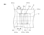
本発明の第1実施形態にかかるコイル部品1aについて、図1および図2を参照して説明する。なお、図1はコイル部品1aの平面図、図2はコイル電極4の配線構造を説明するための図で、図1の要部斜視図である。
<First Embodiment>
A
この実施形態にかかるコイル部品1aは、図1および図2に示すように、コイルコア3が埋設された絶縁層2と、コイルコア3の周囲に巻回された2つのコイル電極4とを備え、高周波信号が使用される携帯電話機等の電子機器に搭載される。
As shown in FIGS. 1 and 2, the
絶縁層2は、例えば、エポキシ樹脂などの樹脂で形成され、コイルコア3および後述する複数の金属ピン5a,5bを被覆するように、所定の厚みで形成される。
The insulating
コイルコア3は、Mn−Znフェライト等の一般的なコイルコアとして採用される磁性材料で形成されている。なお、この実施形態のコイルコア3は、環状を成している。
The
コイル電極4は、環状のコイルコア3の周囲を螺旋状に巻回するものであり、絶縁層2の厚み方向に立設された状態でコイルコア3の周囲に配置された複数の金属ピン5a,5bと、複数の上側配線パターン6aおよび複数の下側配線パターン6bとを備える。各金属ピン5a,5bは、Cu、Au、Ag、AlやCu系の合金など、配線電極として一般的に採用される金属材料で形成されている。また、各金属ピン5a,5bは、これらの金属材料のうちのいずれかで形成された金属線材をせん断加工するなどして形成することができる。
The
各上側配線パターン6aは、絶縁層2の上面に形成される。このとき、各上側配線パターン6aは、一端がコイルコア3の内側(本発明の「一方側」に相当)に配置され、他端がコイルコア3の外側(本発明の「他方側」に相当)に配置された状態で周方向に配列される。
Each
各下側配線パターン6bは、各上側配線パターン6aと複数の対を成すように絶縁層2の下面に形成される。このとき、各下側配線パターン6bは、各上側配線パターン6aと同様、一端がコイルコア3の内側に配置され、他端がコイルコア3の外側に配置された状態で周方向に配列される。
Each
各上側、下側配線パターン6a,6bは、例えば、CuやAg等の金属を含有する導電性ペーストを用いたスクリーン印刷により形成することができる。導電性ペーストは、CuやAgで形成されたフィラと有機溶剤などを混合して形成されるため、この実施形態では、各上側、下側配線パターン6a,6bは各金属ピン5a,5bと比較して比抵抗が高い。
Each of the upper and
なお、各上側、下側配線パターン6a,6bは、例えば、絶縁層2の上面(または、下面)に、CuやAg等の金属を含有する導電性ペーストで形成された下地電極と、該下地電極に、例えばCuめっきで積層された表面電極との2層構造で形成されていてもよい。この場合、各上側、下側配線パターン6a,6bを導電性ペーストのみで形成する場合と比較して、抵抗値を低くすることができる。なお、上側配線パターン6aが、本発明の「第1配線パターン」に相当し、下側配線パターン6bが、本発明の「第2配線パターン」に相当する。
Each of the upper and
各金属ピン5a,5bは、コイルコア3の内周面に沿って配列されたもの(以下、内側金属ピン5aという場合もある。)と、コイルコア3の外周面に沿って配列されたもの(以下、外側金属ピン5bという場合もある。)とで構成されている。この実施形態では、各内側金属ピン5aおよび各外側金属ピン5bそれぞれの上端面が、絶縁層2の上面から露出し、各内側金属ピン5aおよび各外側金属ピン5bそれぞれの下端面が、絶縁層2の下面から露出して設けられる。ここで、各内側金属ピン5aそれぞれが、本発明の「一方側導体」に相当し、各外側金属ピン5bそれぞれが、本発明の「他方側導体」に相当する。
Each of the metal pins 5a and 5b is arranged along the inner peripheral surface of the coil core 3 (hereinafter may be referred to as the
各内側金属ピン5aは、各上側配線パターン6aそれぞれの一端と、当該上側配線パターン6aと対を成す下側配線パターン6bの一端とをそれぞれ接続する。対を成す上側、下側配線パターン6a,6bは、平面視で所定の間隔L1で平行に配置されている。各内側金属ピン5aは、対を成す上側、下側配線パターン6a,6bの一端同士を接続できるように、平面視での間隔L1に等しい幅W1を有している。すなわち、接続する上側、下側配線パターン6a,6bの平面視での距離(間隔L1)に応じて各内側金属ピン5aの幅W1が調整されている。
Each
そして、各内側金属ピン5aそれぞれは、接続する上側配線パターン6aとの接触位置(内側金属ピン5aの上端面と上側配線パターン6aとの接触位置)と下側配線パターン6bとの接触位置(内側金属ピン5aの下端面と下側配線パターン6bとの接触位置)とが平面視でずれて配置される。ここで、上述の「内側金属ピン5aの幅W1が、間隔L1に等しい」とは実質的に等しい場合も含む。なお、内側金属ピン5aの幅W1は、間隔L1よりも大きくてもかまわない。
Each
各外側金属ピン5bは、各上側配線パターン6aそれぞれの他端と、当該上側配線パターン6aと対を成す下側配線パターン6bの所定側(この実施形態では、反時計方向)に隣接する下側配線パターン6bの他端とをそれぞれ接続する。そして、各外側金属ピン5bは、各内側金属ピン5aと同様、接続する上側、下側配線パターン6a,6bの平面視での間隔L1に等しい幅W1を有し、接続する上側配線パターン6aとの接触位置(外側金属ピン5bの上端面と上側配線パターン6aとの接触位置)と下側配線パターン6bとの接触位置(外側金属ピン5bの下端面と下側配線パターン6bとの接触位置)とが平面視でずれて配置される。ここで、上述の「外側金属ピン5bの幅W1が、間隔L1に等しい」とは、内側金属ピン5aと同様、実質的に等しい場合も含む。さらに、内側金属ピン5aと同様、外側金属ピン5bの幅W1は、間隔L1よりも大きくてもかまわない。
Each
なお、この実施形態では、各内側、外側金属ピン5a,5bは、横断面が略楕円の柱状に形成されているが、例えば、角柱状などに形成されていてもよい。また、各内側、外側金属ピン5a,5bに相当するものを、ビア導体で形成してもかまわない。
In this embodiment, each of the inner and
以上のような構成により、コイルコア3の周囲を螺旋状に巻回するコイル電極4が形成されるが、この実施形態では、当該コイル電極4の巻数を容易に増やすことができるように、工夫されている。具体的には、図1に示すように、各上側配線パターン6aおよび各下側配線パターン6bの1つ1つが、コイル電極4の巻回軸方向と平行なコイルコア3の中心軸CA1に平面視で直交するように配置されている。換言すれば、各上側、下側配線パターン6a,6bの1つ1つが、平面視でコイルコア3の外周または内周の接線方向に直交する方向に平行に配置されている。よって、従来の課題、すなわち、上側配線パターン6a又は下側配線パターン6bが斜めに配置され、上側配線パターン6aの前記中心軸CA1に対する角度と、下側配線パターン6bの前記中心軸CA1に対する角度が異なることによる、コイル電極4の巻数増加の妨げを低減することができる。なお、各上側、下側配線パターン6a,6bは、中心軸CA1に平面視で略直交または実質的に直交するように配置されていればよい。
With the configuration as described above, the
(コイル部品の製造方法)
次に、コイル部品1aの製造方法の一例について、簡単に説明する。
(Manufacturing method of coil parts)
Next, an example of a method for manufacturing the
まず、平板状の転写板の一方主面に各金属ピン5a,5bを配置する。この場合、各金属ピン5a,5bの上端面を転写板の一方主面に固定し、各金属ピン5a,5bを立った状態で固定する。なお、各金属ピン5a,5bは例えば、横断面が略楕円状の金属線材(例えば、Cu)をせん断加工するなどして形成することができる。
First, the metal pins 5a and 5b are arranged on one main surface of the flat transfer plate. In this case, the upper end surfaces of the metal pins 5a and 5b are fixed to one main surface of the transfer plate, and the metal pins 5a and 5b are fixed in a standing state. Each
次に、離型層付き樹脂シート(平板状)の一方主面に樹脂層を形成する。この場合、樹脂シート、離型層、樹脂層の順番で配置し、樹脂層を未硬化状態で形成する。 Next, a resin layer is formed on one main surface of the resin sheet with a release layer (flat plate shape). In this case, the resin sheet, the release layer, and the resin layer are arranged in this order, and the resin layer is formed in an uncured state.
次に、各金属ピン5a,5bの下端面と樹脂層とが当接するように、転写板を樹脂シート上に反転搭載後、樹脂層の樹脂を硬化させる。 Next, after mounting the transfer plate on the resin sheet so that the lower end surfaces of the metal pins 5a and 5b are in contact with the resin layer, the resin of the resin layer is cured.
次に、転写板を剥離した後、樹脂シート上の所定位置にコイルコア3を配置し、例えばエポキシ樹脂で各金属ピン5a,5bおよびコイルコア3をモールドして、樹脂シート上に絶縁層2を形成する。
Next, after peeling off the transfer plate, the
次に、離型層付き樹脂シートを剥離し、絶縁層2の表裏面を研磨または研削する。これにより、各金属ピン5a,5bの上端面が絶縁層2の上面から露出し、下端面が絶縁層2の下面から露出する。
Next, the resin sheet with a release layer is peeled off, and the front and back surfaces of the insulating
最後に、絶縁層2の上面に各上側配線パターン6aを形成し、絶縁層2の下面に各下側配線パターン6bを形成してコイル部品1aが完成する。各上側、下側配線パターン6a,6bは、例えば、Cu等の金属を含有する導電性ペーストを用いたスクリーン印刷などで形成することができる。また、この導電性ペーストで形成された配線パターン上にCuめっきを施すことで、各上側、下側配線パターン6a,6bを2層構造にしてもよい。また、各上側、下側配線パターン6a,6bの形成方法の他の例としては、例えば、板状部材の一方主面にCu箔を張り付けたものをエッチングにより所定のパターン形状(上側または下側配線パターン6a,6bの形状)に加工する。この板状部材は各上側、下側配線パターン6a,6bで個別に用意する。この場合、各上側、下側配線パターン6a,6bは、前記板状部材を用いた超音波接合により、各金属ピン5a,5bの上端面または下端面に接合することができる。
Finally, each
したがって、上記した実施形態によれば、各上側配線パターン6aだけでなく、各下側配線パターン6bもコイルコア3の中心軸CA1に平面視で直交するように配置される。そして、各上側配線パターン6aと各下側配線パターン6bとが平面視で同じ方向に配置されるため、従来と比較してコイル電極4の巻数を容易に増やすことができる。
Therefore, according to the above-described embodiment, not only the
また、この種のコイル部品では、コイル電極全体の抵抗値を下げることでコイル特性(例えば、Q値)を向上することができる。そのため、この実施形態のように、各上側、下側配線パターン6a,6bの比抵抗が高い場合は、各上側、下側配線パターン6a,6bの長さを短くするとコイル特性の向上を図ることができる。この点、この実施形態では、各上側、下側配線パターン6a,6bをコイルコア3の前記中心軸CA1に平面視で直交するように配置することで、斜めに配置する従来例と比べて、内側金属ピン5aと外側金属ピン5bとの接続距離を短くすることができる。すなわち、コイル電極4全体の長さの中で、比抵抗の高い各上側、下側配線パターン6a,6bの占める部分を少なくすることができるため、コイル特性の向上を図ることができる。
In this type of coil component, coil characteristics (for example, Q value) can be improved by lowering the resistance value of the entire coil electrode. Therefore, when the specific resistance of the upper and
また、各内側、外側金属ピン5a,5bの幅W1が、接続する上側、下側配線パターン6a,6bの平面視での間隔L1とほぼ等しく、または間隔L1よりも大きく形成されるため、接続する上側、下側配線パターン6a,6bが平面視でずれて配置されている場合であっても、容易に接続することができる。また、幅W1が、間隔L1と略等しくまたは大きくなるように各内側、外側金属ピン5a,5bを幅広に形成することで、コイル電極4全体の長さの中で、比抵抗の高い各上側、下側配線パターン6a,6bの占める部分を少なくすることができるため、コイル電極4全体の抵抗値を低くすることができる。
Further, the width W1 of each inner and
また、各上側配線パターン6aそれぞれは、平面視でいずれの下側配線パターン6bにも重ならない位置に配置されているため、上側配線パターン6aと下側配線パターン6bとの間に生じる寄生容量を低減することができる。
In addition, each
また、金属ピン5a,5bの場合は、絶縁層2に貫通孔の形成が必要なビア導体やスルーホール導体と比較して隣接する金属ピン5a,5b間のギャップを狭くするのが容易であるため、コイル電極4の巻数を容易に増やすことができる。また、例えば図1に示す通り、金属ピン5a、5bの横断面を略楕円もしくは略矩形状とすることで、上側、下側配線パターン6a,6bを形成できる最小Gapにした上で、各上側、下側配線パターン6a,6bを結線することができる。また、金属ピン5a,5bは、ビアホールに導電性ペーストを充填して成るビア導体やスルーホール導体と比較して比抵抗が低いため、コイル電極4全体としての抵抗値を下げることができる。そのため、例えば、Q値などのコイル特性が優れたコイル部品1aを提供することができる。
Further, in the case of the metal pins 5a and 5b, it is easy to narrow the gap between the
(金属ピンの変形例)
次に、金属ピン5a,5bの変形例について、図3および図4を参照して説明する。なお、図3および図4は金属ピンの変形例を説明するための図であって、それぞれ図2に対応する図である。
(Modification of metal pin)
Next, modified examples of the metal pins 5a and 5b will be described with reference to FIGS. 3 and 4 are diagrams for explaining a modification example of the metal pin, each corresponding to FIG.
上記した実施形態では、各金属ピン5a,5bが、横断面が楕円の柱状に形成されている場合について説明したが、各金属ピン5a,5bの形状は、適宜、変更することができる。例えば、図3に示すように、各金属ピン50a,50bがL字状に形成されていてもよい。また、図4に示すように、各金属ピン51a,51bの長さ方向でくびれを有していてもよい。これらの構造であっても、第1実施形態と同様、接続する上側、下側配線パターン6a,6bが平面視でずれて配置されていても両者を容易に接続することができる。
In the above-described embodiment, the case where each of the metal pins 5a and 5b is formed in a columnar shape having an elliptical cross section has been described, but the shape of each of the metal pins 5a and 5b can be changed as appropriate. For example, as shown in FIG. 3, each
<第2実施形態>
本発明の第2実施形態にかかるコイル部品1bについて、図5を参照して説明する。なお、図5はコイル部品1bの平面図である。
Second Embodiment
A
この実施形態にかかるコイル部品1bが、図1および図2を参照して説明した第1実施形態のコイル部品1aと異なるところは、図5に示すように、各金属ピン52a,52bが、円柱状に形成されていることである。その他の構成は、第1実施形態と同じであるため、同一符号を付すことにより説明を省略する。
The
この場合、各金属ピン52a,52bそれぞれは、上端面が上側配線パターン6aに接続され、下端面が下側配線パターン6bに接続される。また、各金属ピン52a,52bの横断面の直径Rは、接続する上側、下側配線パターン6a,6bの平面視での間隔L1と略等しい大きさで形成されている。
In this case, each
このように、各金属ピン52a,52bを円柱状に形成する場合は、横断面の直径Rの大きさを調整することにより、第1実施形態のコイル部品1aと同様の効果を得ることができる。
Thus, when each
<第3実施形態>
本発明の第3実施形態にかかるコイル部品1cについて、図6を参照して説明する。なお、図6はコイル部品1cの平面図である。
<Third Embodiment>
A
この実施形態にかかるコイル部品1cが、図1および図2を参照して説明した第1実施形態のコイル部品1aと異なるところは、図6に示すように、コイルコア3が円環状に形成されていることと、各金属ピン53a,53bが、横断面が横長矩形状を有する角柱状に形成されていることとである。その他の構成は、第1実施形態のコイル部品1aと同じであるため、同一符号を付すことにより説明を省略する。
The
この場合、各上側、下側配線パターン6a,6bは、コイル電極4の巻回軸方向と平行なコイルコア3の中心軸CA2に平面視で直交するように配置されている。具体的には、図6に示すように、上側配線パターン6aと前記中心軸CA2との交点Aの接線TLに対して、当該上側配線パターン6aが直交するように配置される。各下側配線パターン6bも同様である。
In this case, the upper and
また、各金属ピン53a,53bの横断面のサイズ(長手方向の長さ)は、第1実施形態と同様、接続する上側、下側配線パターン6a,6bの平面視での間隔に合わせて調整されている。
Further, the size (longitudinal length) of the cross section of each
この構成によると、コイルコア3を円環状に構成した場合に、第1実施形態のコイル部品1aと同様の効果を得ることができる。
According to this configuration, when the
<第4実施形態>
本発明の第4実施形態にかかるコイル部品1dについて、図7および図8を参照して説明する。なお、図7はコイル部品1dの平面図、図8は図7の上側配線パターン6aの平面図である。
<Fourth embodiment>
A
この実施形態にかかるコイル部品1dが、図1および図2を参照して説明した第1実施形態のコイル部品1aと異なるところは、図7に示すように、各上側、下側配線パターン6a,6bの構成が異なることと、各金属ピン54a,54bの形状が異なることとである。その他の構成は、第1実施形態のコイル部品1aと同じであるため、同一符号を付すことにより説明を省略する。
The
各上側、下側配線パターン6a,6bは、平面視でL字状に形成される。例えば、図8に示すように、各上側配線パターン6aは、コイルコア3の前記中心軸CA1方向と直交する線状の本体部6a1と、その一端が本体部6a1の他端に接続されてL字状を成す屈曲部6a2とを有する。そして、本体部6a1の一端が内側金属ピン54aの上端面に接続されるとともに、屈曲部6a2の他端が外側金属ピン54bの上端面に接続される。各下側配線パターン6bも同様に、本体部6b1と屈曲部6b2とを有し、L字状に形成される。
The upper and
また、この実施形態では、各金属ピン54a,54bそれぞれは、円柱状に形成されており、その横断面は、第1実施形態の金属ピン5a,5bの横断面よりも小さいものが使用されている。 In this embodiment, each of the metal pins 54a and 54b is formed in a columnar shape, and the cross section thereof is smaller than that of the metal pins 5a and 5b of the first embodiment. Yes.
コイル電極4の接続構造について具体的に説明すると、各上側配線パターン6aの本体部6a1は、平面視でいずれの下側配線パターン6bの本体部6b1にも重ならないように配置される。各上側配線パターン6aそれぞれの屈曲部6a2の他端は、平面視で1つの下側配線パターン6bの本体部6b1の一端(屈曲部6b2と接続しない方の端)と重なるように配置され、この重なったところで両者6a,6bが外側金属ピン54bにより接続される。これに対し、各下側配線パターン6bそれぞれの屈曲部6b2の他端は、平面視で1つの上側配線パターン6aの本体部6a1の一端(屈曲部6a2と接続しない方の端)と重なるように配置され、この重なったところで両者6a,6bが内側金属ピン54aにより接続される。
The connection structure of the
この構成によると、各金属ピン5a,5bを細くしつつ、各上側配線パターン6aと各下側配線パターン6bとの平面視での重なりを少なくすることができる。また、各上側、下側配線パターン6a,6bに屈曲部6a2,6b2を設けることで、各上側、下側配線パターン6a,6bの平面視での重なりを容易に減らすことができる。
According to this configuration, it is possible to reduce the overlap of each
(上側、下側配線パターンの変形例)
次に、コイル部品1dの各上側、下側配線パターン6a,6bの変形例について、図9を参照して説明する。なお、図9は部分平面図である。
(Modified example of upper and lower wiring patterns)
Next, a modification of the upper and
上記した実施形態では、各上側、下側配線パターン6a,6bが、L字状に形成される場合について説明したが、各上側、下側配線パターン6a,6bそれぞれを、接続する内側、外側金属ピン54a,54bの平面視での間隔L2と略同じ幅W2を有する短冊状に形成してもかまわない。
In the above-described embodiment, the case where the upper and
この場合、接続される上側、下側配線パターン6a,6bの一部が平面視で重なるように配置される。そして、この重なったところに内側または外側金属ピン54a,54bが配置され、当該内側または外側金属ピン54a,54bにより、両配線パターン6a,6bが接続される。
In this case, the upper and
なお、本発明は上記した各実施形態に限定されるものではなく、その趣旨を逸脱しない限りにおいて、上記したもの以外に種々の変更を行なうことが可能である。例えば、上記した各実施形態では、コイルコア3が環状を有する場合について説明したが、棒状に形成されていてもよい。この場合のコイル部品の形状は、図2〜図4に示した、コイル部品1aの要部斜視図と略同様の形状になる。
The present invention is not limited to the above-described embodiments, and various modifications other than those described above can be made without departing from the spirit of the invention. For example, in each of the above-described embodiments, the case where the
また、絶縁層2を、例えば、セラミック材料で形成してもかまわない。
Further, the insulating
また、本発明は、コイルコアが埋設された絶縁層と、コイルコアの周囲に巻回されたコイル電極とを備える種々のコイル部品に広く適用することができる。 In addition, the present invention can be widely applied to various coil components including an insulating layer in which a coil core is embedded and a coil electrode wound around the coil core.
1a〜1d コイル部品
2 絶縁層
3 コイルコア
4 コイル電極
5a,50a,51a,52a,53a,54a 内側金属ピン(一方側導体)
5b,50b,51b,52b,53b,54b 外側金属ピン(他方側導体)
6a 上側配線パターン(第1配線パターン)
6b 下側配線パターン(第2配線パターン)
6a1,6b1 本体部
6a2,6b2 屈曲部
1a to
5b, 50b, 51b, 52b, 53b, 54b Outer metal pin (other side conductor)
6a Upper wiring pattern (first wiring pattern)
6b Lower wiring pattern (second wiring pattern)
6a1, 6b1 body part 6a2, 6b2 bent part
Claims (5)
前記コイルコアの周囲に巻回されたコイル電極とを備え、
前記コイル電極は、
一端が前記コイルコアの一方側に配置されるとともに他端が前記コイルコアの他方側に配置され、前記絶縁層の一方主面に配列された複数の第1配線パターンと、
一端が前記コイルコアの一方側に配置されるとともに他端が前記コイルコアの他方側に配置され、前記各第1配線パターンそれぞれと複数の対を成すように前記絶縁層の他方主面に配列された複数の第2配線パターンと、
前記コイルコアの前記一方側に配置され、前記各第1配線パターンそれぞれの一端と、当該第1配線パターンと対を成す前記第2配線パターンの一端とを接続する複数の一方側導体と、
前記コイルコアの前記他方側に配置され、前記各第1配線パターンそれぞれの他端と、当該第1配線パターンと対を成す前記第2配線パターンに隣接する前記第2配線パターンの他端とを接続する複数の他方側導体とを有し、
前記各第1配線パターンおよび前記各第2配線パターンが、前記コイルコアの前記コイル電極の巻回軸方向と平行な中心軸に平面視で直交するように配置され、
前記各一方側導体および前記各他方側導体は、対を成す前記第1配線パターンと前記第2配線パターンとの平面視での間隔に等しい幅を有して、前記第1配線パターンとの接触位置と、前記第2配線パターンとの接触位置とが平面視でずれて配置されていることを特徴とするコイル部品。 An insulating layer with a coil core embedded therein;
A coil electrode wound around the coil core,
The coil electrode is
A plurality of first wiring patterns having one end disposed on one side of the coil core and the other end disposed on the other side of the coil core and arranged on one main surface of the insulating layer;
One end is disposed on one side of the coil core and the other end is disposed on the other side of the coil core, and is arranged on the other main surface of the insulating layer so as to form a plurality of pairs with each of the first wiring patterns. A plurality of second wiring patterns;
A plurality of one-side conductors arranged on the one side of the coil core and connecting one end of each first wiring pattern and one end of the second wiring pattern paired with the first wiring pattern;
Arranged on the other side of the coil core to connect the other end of each of the first wiring patterns and the other end of the second wiring pattern adjacent to the second wiring pattern that forms a pair with the first wiring pattern A plurality of other side conductors,
The first wiring patterns and the second wiring patterns are arranged so as to be orthogonal to a central axis parallel to a winding axis direction of the coil electrode of the coil core in a plan view ,
Each of the one-side conductors and each of the other-side conductors have a width equal to a distance in plan view between the first wiring pattern and the second wiring pattern that form a pair, and contact with the first wiring pattern The coil component , wherein the position and the contact position with the second wiring pattern are shifted from each other in plan view .
前記コイルコアの周囲に巻回されたコイル電極とを備え、 A coil electrode wound around the coil core,
前記コイル電極は、 The coil electrode is
一端が前記コイルコアの一方側に配置されるとともに他端が前記コイルコアの他方側に配置され、前記絶縁層の一方主面に配列された複数の第1配線パターンと、 A plurality of first wiring patterns having one end disposed on one side of the coil core and the other end disposed on the other side of the coil core and arranged on one main surface of the insulating layer;
一端が前記コイルコアの一方側に配置されるとともに他端が前記コイルコアの他方側に配置され、前記各第1配線パターンそれぞれと複数の対を成すように前記絶縁層の他方主面に配列された複数の第2配線パターンと、 One end is disposed on one side of the coil core and the other end is disposed on the other side of the coil core, and is arranged on the other main surface of the insulating layer so as to form a plurality of pairs with each of the first wiring patterns. A plurality of second wiring patterns;
前記コイルコアの前記一方側に配置され、前記各第1配線パターンそれぞれの一端と、当該第1配線パターンと対を成す前記第2配線パターンの一端とを接続する複数の一方側導体と、 A plurality of one-side conductors arranged on the one side of the coil core and connecting one end of each first wiring pattern and one end of the second wiring pattern paired with the first wiring pattern;
前記コイルコアの前記他方側に配置され、前記各第1配線パターンそれぞれの他端と、当該第1配線パターンと対を成す前記第2配線パターンに隣接する前記第2配線パターンの他端とを接続する複数の他方側導体とを有し、 Arranged on the other side of the coil core to connect the other end of each of the first wiring patterns and the other end of the second wiring pattern adjacent to the second wiring pattern that forms a pair with the first wiring pattern A plurality of other side conductors,
前記各第1配線パターンおよび前記各第2配線パターンが、前記コイルコアの前記コイル電極の巻回軸方向と平行な中心軸に平面視で直交するように配置され、 The first wiring patterns and the second wiring patterns are arranged so as to be orthogonal to a central axis parallel to a winding axis direction of the coil electrode of the coil core in a plan view,
前記各一方側導体および前記各他方側導体は、対を成す前記第1配線パターンと前記第2配線パターンとの平面視での間隔よりも大きい幅を有して、前記第1配線パターンとの接触位置と、前記第2配線パターンとの接触位置とが平面視でずれて配置されていることを特徴とするコイル部品。 Each of the one-side conductors and each of the other-side conductors has a width larger than a distance in plan view between the first wiring pattern and the second wiring pattern that form a pair, and the first wiring pattern The coil component, wherein the contact position and the contact position with the second wiring pattern are shifted from each other in plan view.
3. The coil component according to claim 1, wherein a specific resistance of each of the one side conductor and the other side conductor is smaller than a specific resistance of each of the first and second wiring patterns.
Each one side conductor and the respective other side conductor, a coil component according to any of claims 1 to 4, characterized in that it is formed by a metal pin.
Priority Applications (1)
| Application Number | Priority Date | Filing Date | Title |
|---|---|---|---|
| JP2014222717A JP6439384B2 (en) | 2014-10-31 | 2014-10-31 | Coil parts |
Applications Claiming Priority (1)
| Application Number | Priority Date | Filing Date | Title |
|---|---|---|---|
| JP2014222717A JP6439384B2 (en) | 2014-10-31 | 2014-10-31 | Coil parts |
Publications (2)
| Publication Number | Publication Date |
|---|---|
| JP2016092104A JP2016092104A (en) | 2016-05-23 |
| JP6439384B2 true JP6439384B2 (en) | 2018-12-19 |
Family
ID=56018904
Family Applications (1)
| Application Number | Title | Priority Date | Filing Date |
|---|---|---|---|
| JP2014222717A Active JP6439384B2 (en) | 2014-10-31 | 2014-10-31 | Coil parts |
Country Status (1)
| Country | Link |
|---|---|
| JP (1) | JP6439384B2 (en) |
Families Citing this family (1)
| Publication number | Priority date | Publication date | Assignee | Title |
|---|---|---|---|---|
| CN111834339A (en) * | 2019-04-23 | 2020-10-27 | 福建省福联集成电路有限公司 | Inductor structure for integrated circuit and manufacturing method |
Family Cites Families (4)
| Publication number | Priority date | Publication date | Assignee | Title |
|---|---|---|---|---|
| EP0725407A1 (en) * | 1995-02-03 | 1996-08-07 | International Business Machines Corporation | Three-dimensional integrated circuit inductor |
| JP2002100733A (en) * | 2000-09-21 | 2002-04-05 | Nec Corp | High-frequency ic device |
| US7821374B2 (en) * | 2007-01-11 | 2010-10-26 | Keyeye Communications | Wideband planar transformer |
| JP2014038884A (en) * | 2012-08-10 | 2014-02-27 | Murata Mfg Co Ltd | Electronic component and method for manufacturing electronic component |
-
2014
- 2014-10-31 JP JP2014222717A patent/JP6439384B2/en active Active
Also Published As
| Publication number | Publication date |
|---|---|
| JP2016092104A (en) | 2016-05-23 |
Similar Documents
| Publication | Publication Date | Title |
|---|---|---|
| JP6323553B2 (en) | Coil parts | |
| JP6540808B2 (en) | Flexible inductor | |
| JP6827487B2 (en) | Manufacturing method using magnetic device and flex circuit | |
| US11056261B2 (en) | Inductor | |
| JP6365692B2 (en) | Coil parts | |
| JP2016051765A (en) | Inductor component | |
| JP6551546B2 (en) | Inductor component and method of manufacturing the same | |
| JP6414645B2 (en) | Inductor component and manufacturing method thereof | |
| JP6292300B2 (en) | Coil component and module including the coil component | |
| JP6428792B2 (en) | Coil parts | |
| JP6406354B2 (en) | Inductor parts | |
| JP6439384B2 (en) | Coil parts | |
| JP6390715B2 (en) | Coil parts | |
| JP6521104B2 (en) | Inductor component and method of manufacturing the same | |
| JP6447090B2 (en) | Coil parts | |
| JP6607312B2 (en) | Inductor parts | |
| WO2016068067A1 (en) | Coil component | |
| JP6520130B2 (en) | Coil parts | |
| JPWO2019131581A1 (en) | Inductor bridge and electronics | |
| JP6573027B2 (en) | Inductor parts | |
| JP6432674B2 (en) | Inductor parts | |
| JP6504270B2 (en) | Inductor component and method of manufacturing the same | |
| JP2005072032A (en) | Thin-film core inductor and manufacturing method thereof |
Legal Events
| Date | Code | Title | Description |
|---|---|---|---|
| A621 | Written request for application examination |
Free format text: JAPANESE INTERMEDIATE CODE: A621 Effective date: 20170707 |
|
| A977 | Report on retrieval |
Free format text: JAPANESE INTERMEDIATE CODE: A971007 Effective date: 20180709 |
|
| A131 | Notification of reasons for refusal |
Free format text: JAPANESE INTERMEDIATE CODE: A131 Effective date: 20180807 |
|
| A521 | Written amendment |
Free format text: JAPANESE INTERMEDIATE CODE: A523 Effective date: 20181004 |
|
| TRDD | Decision of grant or rejection written | ||
| A01 | Written decision to grant a patent or to grant a registration (utility model) |
Free format text: JAPANESE INTERMEDIATE CODE: A01 Effective date: 20181023 |
|
| A61 | First payment of annual fees (during grant procedure) |
Free format text: JAPANESE INTERMEDIATE CODE: A61 Effective date: 20181105 |
|
| R150 | Certificate of patent or registration of utility model |
Ref document number: 6439384 Country of ref document: JP Free format text: JAPANESE INTERMEDIATE CODE: R150 |