JP6418968B2 - Electronic component mounting package, electronic device and electronic module - Google Patents

Electronic component mounting package, electronic device and electronic module Download PDF

Info

Publication number
JP6418968B2
JP6418968B2 JP2015015635A JP2015015635A JP6418968B2 JP 6418968 B2 JP6418968 B2 JP 6418968B2 JP 2015015635 A JP2015015635 A JP 2015015635A JP 2015015635 A JP2015015635 A JP 2015015635A JP 6418968 B2 JP6418968 B2 JP 6418968B2
Authority
JP
Japan
Prior art keywords
external circuit
electronic component
connection electrode
base
circuit connection
Prior art date
Legal status (The legal status is an assumption and is not a legal conclusion. Google has not performed a legal analysis and makes no representation as to the accuracy of the status listed.)
Active
Application number
JP2015015635A
Other languages
Japanese (ja)
Other versions
JP2016139771A (en
Inventor
拓治 岡村
拓治 岡村
智仁 吉田
智仁 吉田
Current Assignee (The listed assignees may be inaccurate. Google has not performed a legal analysis and makes no representation or warranty as to the accuracy of the list.)
Kyocera Corp
Original Assignee
Kyocera Corp
Priority date (The priority date is an assumption and is not a legal conclusion. Google has not performed a legal analysis and makes no representation as to the accuracy of the date listed.)
Filing date
Publication date
Application filed by Kyocera Corp filed Critical Kyocera Corp
Priority to JP2015015635A priority Critical patent/JP6418968B2/en
Publication of JP2016139771A publication Critical patent/JP2016139771A/en
Application granted granted Critical
Publication of JP6418968B2 publication Critical patent/JP6418968B2/en
Active legal-status Critical Current
Anticipated expiration legal-status Critical

Links

Images

Description

本発明は、電子部品、例えばCCD(Charge Coupled Device)型またはCMOS(Complementary Metal Oxide Semiconductor)型等の撮像素子、LED(Light Emitting Diode)等の発光素子等の電子部品が実装される電子部品実装用パッケージ、電子装
置および電子モジュールに関するものである。
The present invention is an electronic component mounting in which an electronic component, for example, an image pickup device such as a CCD (Charge Coupled Device) type or a CMOS (Complementary Metal Oxide Semiconductor) type, or a light emitting device such as an LED (Light Emitting Diode) is mounted. The present invention relates to an electronic package, an electronic device, and an electronic module.

従来から電子部品が実装される基体と、基体の下面に設けられた外部回路接続用電極とを有する電子部品実装用パッケージが知られている。また、電子部品実装用パッケージは、下面に設けられた外部回路接続用電極と、外部回路基板とをハンダ等の外部回路接合部材を介して接合する構造が知られている。   2. Description of the Related Art Conventionally, an electronic component mounting package having a base on which an electronic component is mounted and an external circuit connection electrode provided on the lower surface of the base is known. In addition, an electronic component mounting package has a known structure in which an external circuit connection electrode provided on a lower surface and an external circuit board are joined via an external circuit joining member such as solder.

特開2001−189550号公報JP 2001-189550 A

一般的に、電子部品実装用パッケージを含む電子装置を外部回路基板に実装する工程において、熱を加える工程がある。さらに、近年、電子部品は高機能化に伴い、電子部品が作動する際に発生する熱が大きくなっており、これら2点のことから電子装置および外部回路基板に熱が加わる機会は少なくない。また、一般的に電子部品実装用パッケージと外部回路基板とでは、熱膨張率が異なる。よって、この電子部品が作動する際に発生する熱による熱膨張の大きさが、電子部品実装用パッケージと外部回路基板との間で異なる。このことで、電子部品実装用パッケージと外部回路基板との間の外部回路接合部材、電子部品実装用パッケージの下面に設けられた外部回路接続用電極、または外部回路基板の接続電極にクラックまたは剥離が発生し、電子装置と外部回路基板を実装する工程における熱、または電子装置を使用する際の熱による信頼性の低下が懸念されていた。   Generally, there is a step of applying heat in a step of mounting an electronic device including an electronic component mounting package on an external circuit board. Furthermore, in recent years, as electronic components become more sophisticated, heat generated when the electronic components operate increases, and there are not a few opportunities for heat to be applied to the electronic device and the external circuit board because of these two points. In general, the electronic component mounting package and the external circuit board have different coefficients of thermal expansion. Therefore, the magnitude of thermal expansion due to heat generated when the electronic component is operated differs between the electronic component mounting package and the external circuit board. As a result, the external circuit bonding member between the electronic component mounting package and the external circuit board, the external circuit connection electrode provided on the lower surface of the electronic component mounting package, or the connection electrode of the external circuit board is cracked or peeled off. As a result, there has been a concern about reliability degradation due to heat in the process of mounting the electronic device and the external circuit board or heat when using the electronic device.

本発明の1つの態様に係る電子部品実装用パッケージは、電子部品が実装される基体と、該基体の下面に設けられた外部回路接続用電極と、前記基体の下面かつ平面視において前記外部接続用電極と重なる位置に、前記外部接続用電極よりも小さい貫通孔を有する絶縁層とを有し、該外部回路接続用電極は、前記基体との間に間隙を有するように、前記基体に取り囲まれている。 An electronic component mounting package according to an aspect of the present invention includes a base on which an electronic component is mounted, an external circuit connection electrode provided on a lower surface of the base, and the external connection in the lower surface and the plan view of the base. And an insulating layer having a through hole smaller than the external connection electrode at a position overlapping with the external electrode , and the external circuit connection electrode is surrounded by the base so as to have a gap between the base and the base. It is.

本発明の1つの態様に係る電子装置は、上記の電子部品実装用パッケージと、該電子部品実装用パッケージに実装された前記電子部品とを有する。   An electronic device according to one aspect of the present invention includes the electronic component mounting package described above and the electronic component mounted on the electronic component mounting package.

本発明の電子部品実装用パッケージは、電子部品が実装される基体と、基体の下面に設けられた外部回路接続用電極とを有し、外部回路接続用電極は、基体との間に間隙を有するように、基体に取り囲まれている。これにより、電子部品が作動し、発熱した場合において、基体と外部回路接続用電極との間に間隙を有することで電子部品の発熱による基体と外部回路基板との熱膨張差による応力を外部回路接続用電極が傾くことにより吸収することができ、電子部品実装用パッケージと外部回路基板との間の外部回路接合部材、電子部品実装用パッケージの下面に設けられた外部回路接続用電極、または外部回路基板の接続電極にかかる応力を低減させることが可能となる。よって、外部回路接合部材、外部回路接続用電極、または接続電極にクラックまたは剥離が発生することを低減させることが
できる。
The electronic component mounting package of the present invention has a base on which the electronic component is mounted and an external circuit connection electrode provided on the lower surface of the base, and the external circuit connection electrode has a gap between the base and the base. It is surrounded by a substrate to have. As a result, when the electronic component is activated and generates heat, a gap is provided between the base and the external circuit connection electrode, so that the stress due to the thermal expansion difference between the base and the external circuit board due to heat generation of the electronic component can be reduced. It can be absorbed by the inclination of the connection electrode, and an external circuit joint member between the electronic component mounting package and the external circuit board, an external circuit connection electrode provided on the lower surface of the electronic component mounting package, or the outside It is possible to reduce the stress applied to the connection electrode of the circuit board. Therefore, it is possible to reduce the occurrence of cracks or peeling in the external circuit bonding member, the external circuit connection electrode, or the connection electrode.

本発明の1つの態様に係る電子装置は、上述の電子部品実装用パッケージを有することにより、電子部品が作動時の発熱に外部回路接続部材等のストレスを緩和することが可能となり、電子装置の連続使用による信頼性の向上を図ることが可能となる。   An electronic device according to one aspect of the present invention includes the above-described electronic component mounting package, whereby the electronic component can relieve stress generated by an external circuit connection member due to heat generated during operation. It becomes possible to improve the reliability by continuous use.

(a)は、本発明の第1の実施形態に係る電子部品実装用パッケージ、および電子装置の外観を示す上面図であり、(b)は、(a)のA−A線に対応する縦断面図である。(A) is a top view which shows the external appearance of the electronic component mounting package and electronic device which concern on the 1st Embodiment of this invention, (b) is a longitudinal section corresponding to the AA line of (a) FIG. (a)は、本発明の第1の実施形態に係る電子部品実装用パッケージ、および電子装置と外部回路基板とが接合された一例を示す上面図であり、(b)は、(a)のA−A線に対応する縦断面図である。(A) is a top view which shows an example in which the electronic component mounting package according to the first embodiment of the present invention and the electronic device and the external circuit board are joined, and (b) is a diagram of (a). It is a longitudinal cross-sectional view corresponding to an AA line. 本発明の第2の実施形態に係る電子部品実装用パッケージ、および電子装置の外観を示す縦断面図である。It is a longitudinal cross-sectional view which shows the external appearance of the electronic component mounting package which concerns on the 2nd Embodiment of this invention, and an electronic device. (a)及び(b)は、それぞれ本発明の第2の実施形態のその他の形態に係る電子装置の外観を示す縦断面図である。(A) And (b) is a longitudinal cross-sectional view which shows the external appearance of the electronic device which concerns on the other form of the 2nd Embodiment of this invention, respectively. 本発明の第3の実施形態に係る電子部品実装用パッケージ、および電子装置の外観を示す縦断面図である。It is a longitudinal cross-sectional view which shows the external appearance of the electronic component mounting package which concerns on the 3rd Embodiment of this invention, and an electronic device. (a)は、本発明の第4の実施形態に係る電子部品実装用パッケージ、および電子装置の外観を示す上面図であり、(b)は、(a)のA−A線に対応する縦断面図である。(A) is a top view which shows the external appearance of the electronic component mounting package and electronic device which concern on the 4th Embodiment of this invention, (b) is a longitudinal section corresponding to the AA line of (a) FIG. (a)は、本発明の第5の実施形態に係る電子部品実装用パッケージ、および電子装置の外観を示す上面図であり、(b)は、(a)のA−A線に対応する縦断面図である。(A) is a top view which shows the external appearance of the electronic component mounting package and electronic device which concern on the 5th Embodiment of this invention, (b) is a longitudinal section corresponding to the AA line of (a) FIG. 本発明の第6の実施形態に係る電子部品実装用パッケージ、および電子装置の外観を示す縦断面図である。It is a longitudinal cross-sectional view which shows the external appearance of the electronic component mounting package which concerns on the 6th Embodiment of this invention, and an electronic device. 本発明の第7の実施形態に係る電子部品実装用パッケージ、および電子装置の縦断面図である。It is a longitudinal cross-sectional view of the electronic component mounting package and electronic device which concern on the 7th Embodiment of this invention. (a)及び(b)はそれぞれ本発明の実施形態に係る電子部品実装用パッケージ、および電子装置の一例を示す下面図である。(A) And (b) is a bottom view which shows an example of the electronic component mounting package and electronic device which concern on embodiment of this invention, respectively. 本発明の実施形態に係る電子部品実装用パッケージ、および電子装置の一例を示す下面図である。1 is a bottom view illustrating an example of an electronic component mounting package and an electronic device according to an embodiment of the present invention.

以下、本発明のいくつかの例示的な実施形態について図面を参照して説明する。なお、以下の説明では、電子部品実装用パッケージに電子部品が実装された構成を電子装置とする。電子部品実装用パッケージおよび電子装置は、いずれの方向が上方若しくは下方とされてもよいものであるが、便宜的に、直交座標系xyzを定義するとともに、z方向の正側を上方として、上面若しくは下面の語を用いるものとする。   Hereinafter, some exemplary embodiments of the present invention will be described with reference to the drawings. In the following description, a configuration in which an electronic component is mounted on an electronic component mounting package is referred to as an electronic device. The electronic component mounting package and the electronic device may be either upward or downward, but for convenience, the orthogonal coordinate system xyz is defined and the positive side in the z direction is defined as the upper surface. Or use the word on the bottom.

(第1の実施形態)
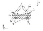
図1および図2を参照して本発明の第1の実施形態における電子装置21、及び電子部品実装用パッケージ1について説明する。本実施形態における電子装置21は、電子部品実装用パッケージ1と電子部品10とを有している。
(First embodiment)
The electronic device 21 and the electronic component mounting package 1 according to the first embodiment of the present invention will be described with reference to FIGS. 1 and 2. The electronic device 21 in this embodiment includes an electronic component mounting package 1 and an electronic component 10.

図1および図2に示す例において、電子部品実装用パッケージ1は、電子部品10が実装される基体2と、基体2の下面に設けられた外部回路接続用電極9とを有し、外部回路接続用電極9は、基体2との間に間隙6を有するように、基体2に取り囲まれている。   In the example shown in FIGS. 1 and 2, the electronic component mounting package 1 includes a base 2 on which the electronic component 10 is mounted and an external circuit connection electrode 9 provided on the lower surface of the base 2. The connection electrode 9 is surrounded by the base body 2 so as to have a gap 6 between the connection electrode 9 and the base body 2.

図1および図2に示す例では、電子部品10が実装される基体2を有している。   In the example shown in FIG. 1 and FIG. 2, it has the base | substrate 2 with which the electronic component 10 is mounted.

基体2は、絶縁基体に後述する配線導体が形成されて成る。この絶縁基体の材料は例えば、電気絶縁性セラミックス、または樹脂等が使用される。   The base 2 is formed by forming a wiring conductor described later on an insulating base. As the material of the insulating base, for example, electrically insulating ceramics or resin is used.

基体2の絶縁基体の材料として使用される電気絶縁性セラミックスとしては例えば、酸化アルミニウム質焼結体,ムライト質焼結体,炭化珪素質焼結体,窒化アルミニウム質焼結体,窒化珪素質焼結体,またはガラスセラミックス焼結体等が挙げられる。   Examples of the electrically insulating ceramic used as the material of the insulating substrate of the substrate 2 include an aluminum oxide sintered body, a mullite sintered body, a silicon carbide sintered body, an aluminum nitride sintered body, and a silicon nitride sintered body. Examples include a sintered body or a glass ceramic sintered body.

基体2の絶縁基体の材料として使用される樹脂としては例えば、エポキシ樹脂,ポリイミド樹脂,アクリル樹脂,フェノール樹脂,またはフッ素系樹脂等が挙げられる。フッ素系樹脂としては例えば、ポリエステル樹脂、または四フッ化エチレン樹脂が挙げられる。   Examples of the resin used as the material of the insulating base of the base 2 include an epoxy resin, a polyimide resin, an acrylic resin, a phenol resin, or a fluorine resin. Examples of the fluorine-based resin include polyester resin and tetrafluoroethylene resin.

図1および図2に示す例では、基体2は、前述した材料から成る絶縁層を複数上下に積層して形成されている。   In the example shown in FIGS. 1 and 2, the base 2 is formed by laminating a plurality of insulating layers made of the above-described materials.

基体2は、図1および図2に示す例のように4層の絶縁層から形成されていてもよいし、単層〜3層または5層以上の絶縁層から形成されていてもよい。また、基体2は貫通孔を有する枠体と貫通孔を有さない基部とから形成される凹部を有していてもよく、さらに枠体から成る基体は大きさの異なる枠体を2つ有し、段差部を形成していてもよい。図1および図2に示す例では、この段差部が段差部に電子部品接続用パッド3が設けられている。   The substrate 2 may be formed of four insulating layers as in the examples shown in FIGS. 1 and 2, or may be formed of a single layer to three layers or five or more insulating layers. The base 2 may have a recess formed by a frame having a through hole and a base having no through hole, and the base made of the frame has two frames having different sizes. However, a stepped portion may be formed. In the example shown in FIGS. 1 and 2, this step portion is provided with an electronic component connecting pad 3 at the step portion.

基体2の内部には、各絶縁層間を導通させる貫通導体と内部配線とから成る配線導体が設けられていてもよいし、基体2は、表面に露出した配線導体を有していてもよい。また、基体2を形成する各絶縁層のそれぞれの内部に設けられた配線導体が、各絶縁層の表面に露出した配線導体等によって電気的に接続されていてもよい。   Inside the base body 2, a wiring conductor composed of a through conductor and internal wiring for conducting each insulating layer may be provided, or the base body 2 may have a wiring conductor exposed on the surface. In addition, the wiring conductors provided in the respective insulating layers forming the base 2 may be electrically connected by wiring conductors exposed on the surfaces of the respective insulating layers.

電子部品接続用パッド3及び配線導体は、基体2が電気絶縁性セラミックスから成る場合には、タングステン(W),モリブデン(Mo),マンガン(Mn),銀(Ag)若しくは銅(Cu)、または、これらから選ばれる少なくとも1種以上の金属材料を含有する合金等から成る。また、電子部品接続用パッド3及び配線導体は、基体2が樹脂から成る場合には、銅(Cu),金(Au),アルミニウム(Al),ニッケル(Ni),クロム(Cr),モリブデン(Mo)若しくはチタン(Ti)、または、これらから選ばれる少なくとも1種以上の金属材料を含有する合金等から成る。   When the base 2 is made of an electrically insulating ceramic, the electronic component connecting pad 3 and the wiring conductor are tungsten (W), molybdenum (Mo), manganese (Mn), silver (Ag) or copper (Cu), or And an alloy containing at least one metal material selected from these. The electronic component connecting pad 3 and the wiring conductor are made of copper (Cu), gold (Au), aluminum (Al), nickel (Ni), chromium (Cr), molybdenum (when the base 2 is made of resin). Mo) or titanium (Ti), or an alloy containing at least one metal material selected from these.

電子部品接続用パッド3および配線導体の露出した表面に、めっき層が設けられることが好ましい。この構成によれば、電子部品接続用パッド3および配線導体の露出表面を保護して酸化を防止できる。また、この構成によれば、電子部品接続用パッド3と電子部品10との接続部材13(ワイヤボンディング等)を介した電気的接続を良好にできる。めっき層は、例えば、厚さ0.5〜10μmのNiめっき層を被着させる。または、このNiめっき層の上に、厚さ0.5〜3μmの金(Au)めっき層を被着させてもよい。   It is preferable that a plating layer is provided on the exposed surface of the electronic component connecting pad 3 and the wiring conductor. According to this configuration, the electronic component connection pad 3 and the exposed surface of the wiring conductor can be protected to prevent oxidation. Moreover, according to this structure, the electrical connection through the connection member 13 (wire bonding etc.) of the electronic component connection pad 3 and the electronic component 10 can be improved. As the plating layer, for example, a Ni plating layer having a thickness of 0.5 to 10 μm is deposited. Alternatively, a gold (Au) plating layer having a thickness of 0.5 to 3 μm may be deposited on the Ni plating layer.

図1及び図2に示す例のように、電子部品実装用パッケージ1は凹部に、電子部品10が実装されている。また、図1及び図2に示す例では基体2に設けられた凹部に電子部品10が実装されているが、基体2に凹部を設けず直接基体2の表面に電子部品10を実装しても良い。   As in the example shown in FIGS. 1 and 2, the electronic component mounting package 1 has the electronic component 10 mounted in the recess. In the example shown in FIGS. 1 and 2, the electronic component 10 is mounted in the recess provided in the base 2. However, the electronic component 10 may be mounted directly on the surface of the base 2 without providing the recess in the base 2. good.

図1及び図2に示す例では、電子部品実装用パッケージ1の基体2は下面に設けられた外部回路接続用電極9を有している。   In the example shown in FIGS. 1 and 2, the base 2 of the electronic component mounting package 1 has an external circuit connection electrode 9 provided on the lower surface.

外部回路接続用電極9は、基体2が電気絶縁性セラミックスから成る場合には、タングステン(W),モリブデン(Mo),マンガン(Mn),銀(Ag)若しくは銅(Cu)、または、これらから選ばれる少なくとも1種以上の金属材料を含有する合金等から成る。また、外部回路接続用電極9は、基体2が樹脂から成る場合には、銅(Cu),金(Au),アルミニウム(Al),ニッケル(Ni),クロム(Cr),モリブデン(Mo)若しくはチタン(Ti)、または、これらから選ばれる少なくとも1種以上の金属材料を含有する合金等から成る。   The external circuit connection electrode 9 is made of tungsten (W), molybdenum (Mo), manganese (Mn), silver (Ag), copper (Cu), or the like when the substrate 2 is made of an electrically insulating ceramic. It consists of an alloy containing at least one selected metal material. The external circuit connection electrode 9 is made of copper (Cu), gold (Au), aluminum (Al), nickel (Ni), chromium (Cr), molybdenum (Mo) or the like when the substrate 2 is made of resin. It consists of titanium (Ti) or an alloy containing at least one metal material selected from these.

また、外部回路接続用電極9は電子部品接続用パッド3と前述した内部配線を介して電気的に接続されていてもよい。   The external circuit connection electrode 9 may be electrically connected to the electronic component connection pad 3 via the internal wiring described above.

外部回路接続用電極9の露出した表面に、めっき層が設けられることが好ましい。この構成によれば、外部回路接続用電極9の露出表面を保護して酸化を防止できる。また、この構成によれば、外部回路接続用電極9と外部回路基板20との外部回路接続部材(はんだ等)を介した電気的接続を良好にできる。めっき層は、例えば、厚さ0.5〜10μmのNiめっき層を被着させる。または、このNiめっき層の上に、厚さ0.5〜3μmの金(Au)めっき層を被着させてもよい。   A plating layer is preferably provided on the exposed surface of the external circuit connection electrode 9. According to this configuration, the exposed surface of the external circuit connection electrode 9 can be protected to prevent oxidation. Moreover, according to this structure, the electrical connection between the external circuit connection electrode 9 and the external circuit board 20 through the external circuit connection member (solder or the like) can be improved. As the plating layer, for example, a Ni plating layer having a thickness of 0.5 to 10 μm is deposited. Alternatively, a gold (Au) plating layer having a thickness of 0.5 to 3 μm may be deposited on the Ni plating layer.

図1及び図2では、電子部品実装用パッケージ1の外部回路接続用電極9は、基体2との間に間隙6を有するように、基体2に取り囲まれている。   In FIG. 1 and FIG. 2, the external circuit connection electrode 9 of the electronic component mounting package 1 is surrounded by the base 2 so as to have a gap 6 between the base 2.

図1及び図2に示す例のように、外部回路接続用電極9は、基体2との間に間隙6を有するように、前記基体に取り囲まれていることで、電子装置21を外部回路基板20に実装する工程での加熱、または電子部品実装用パッケージ1に実装される電子部品10が作動し、発熱した場合において、電子部品10の発熱による基体2と外部回路基板20との熱膨張差による応力を外部回路接続用電極9が基体2または外部回路基板20に追従し傾くことにより吸収することができる。このことから電子部品実装用パッケージ1と外部回路基板20との間の外部回路接続部材23、電子部品実装用パッケージ1の下面に設けられた外部回路接続用電極9、または外部回路基板20の接続電極にかかる応力を低減させることが可能となる。よって、外部回路接続部材23、外部回路接続用電極9、または接続電極にクラックまたは剥離が発生することを低減させることができる。   As shown in FIGS. 1 and 2, the external circuit connection electrode 9 is surrounded by the base so as to have a gap 6 between the base 2 and the electronic device 21 is connected to the external circuit board. When the electronic component 10 mounted on the electronic component mounting package 1 is heated in the process of mounting on the electronic component 20 and generates heat, the difference in thermal expansion between the base 2 and the external circuit board 20 due to heat generation of the electronic component 10 The external circuit connecting electrode 9 can absorb the stress caused by the inclination by following the base 2 or the external circuit board 20. Therefore, the external circuit connection member 23 between the electronic component mounting package 1 and the external circuit board 20, the external circuit connection electrode 9 provided on the lower surface of the electronic component mounting package 1, or the connection of the external circuit board 20. It is possible to reduce the stress applied to the electrode. Therefore, it is possible to reduce the occurrence of cracks or peeling in the external circuit connection member 23, the external circuit connection electrode 9, or the connection electrode.

また、間隙6は、電子部品実装用パッケージ1の基体2の熱膨張率と外部回路基板20の熱膨張率との関係によってより好ましい位置が異なる。例えば、基体2の熱膨張率が外部回路基板20の熱膨張率よりも小さい場合、外部回路基板20は基体2よりも熱膨張時の変形が大きい。よって、間隙6は断面視において外部回路接続用電極9の基体2の外縁部側に設けられていることによって、外部回路接続用電極9が熱膨張する方向に追従し傾き、外部回路接続用電極9、または外部回路基板20の接続電極にかかる応力を低減させることが可能となる。また例えば、例えば、基体2の熱膨張率が外部回路基板20の熱膨張率よりも大きい場合、外部回路基板20は基体2よりも熱膨張時の変形が小さい。よって、間隙6は断面視において外部回路接続用電極9の基体2の内側部側に設けられていることによって、外部回路接続用電極9が熱膨張する方向に追従し傾き、外部回路接続用電極9、または外部回路基板20の接続電極にかかる応力を低減させることが可能となる。   The gap 6 has a more preferable position depending on the relationship between the thermal expansion coefficient of the base 2 of the electronic component mounting package 1 and the thermal expansion coefficient of the external circuit board 20. For example, when the thermal expansion coefficient of the base 2 is smaller than the thermal expansion coefficient of the external circuit board 20, the external circuit board 20 is more deformed during thermal expansion than the base 2. Therefore, the gap 6 is provided on the outer edge side of the base body 2 of the external circuit connection electrode 9 in a cross-sectional view, so that the external circuit connection electrode 9 follows and inclines in the direction of thermal expansion, and the external circuit connection electrode 9 or the stress applied to the connection electrode of the external circuit board 20 can be reduced. Further, for example, when the thermal expansion coefficient of the base 2 is larger than the thermal expansion coefficient of the external circuit board 20, the external circuit board 20 is less deformed during thermal expansion than the base 2. Therefore, the gap 6 is provided on the inner side of the base body 2 of the external circuit connection electrode 9 in a cross-sectional view, so that the external circuit connection electrode 9 is inclined following the direction of thermal expansion, and the external circuit connection electrode 9 or the stress applied to the connection electrode of the external circuit board 20 can be reduced.

また、間隙6の大きさは電子部品実装用パッケージ1及び外部回路基板20の熱膨張率から変形の大きさを算出し、その差以上の大きさであることがより好ましい。例えば、基体2と外部回路基板20の熱膨張率の差が15ppmであり、外部回路接続用電極9間の大きさが64mmであり、温度差が200℃であった場合、間隙6は80μm以上設けることが好ましいこととなる。このことによって、電子装置21と外部回路基板20とを接
合する工程での加熱、または電子部品10の作動時の発熱において、外部回路基板20と電子部品実装用パッケージ1の熱膨張差による応力を確実に吸収することができる。
The size of the gap 6 is more preferably larger than the difference obtained by calculating the size of deformation from the thermal expansion coefficients of the electronic component mounting package 1 and the external circuit board 20. For example, when the difference in coefficient of thermal expansion between the base 2 and the external circuit board 20 is 15 ppm, the size between the external circuit connection electrodes 9 is 64 mm, and the temperature difference is 200 ° C., the gap 6 is 80 μm or more. It is preferable to provide it. As a result, the stress due to the difference in thermal expansion between the external circuit board 20 and the electronic component mounting package 1 during the heating in the process of joining the electronic device 21 and the external circuit board 20 or the heat generated when the electronic component 10 is activated. Can be absorbed reliably.

また、外部回路接続用電極9と基体2とは例えば熱硬化性樹脂、または銀エポキシ等のろう材等で接合していても良い。   Further, the external circuit connection electrode 9 and the base 2 may be joined together with, for example, a thermosetting resin or a brazing material such as silver epoxy.

また、図1および図2に示す例では、外部回路接続用電極9の側面と基体2とが接する部分とは接着剤等で固定せず、外部回路接続用電極9の上面と基体2とが接する部分のみで固定していることが好ましい。これは、外部回路接続用電極9が基体2または外部回路基板20に追従して傾くことで電子部品実装用パッケージ1と外部回路基板20との熱膨張差を吸収しやすくなるためである。   In the example shown in FIGS. 1 and 2, the side of the external circuit connection electrode 9 and the portion where the base 2 is in contact are not fixed with an adhesive or the like, and the upper surface of the external circuit connection electrode 9 and the base 2 are not fixed. It is preferable to fix only at the contact part. This is because the external circuit connection electrode 9 is inclined to follow the base 2 or the external circuit board 20 so that the thermal expansion difference between the electronic component mounting package 1 and the external circuit board 20 is easily absorbed.

また、外部回路接続用電極9は平面視において円形、矩形状のいずれであっても良いが、外部回路基板20との接合信頼性の為に、長辺が250μm以上であることが好ましい。またさらに、外部回路接続用電極9は縦断面視において20μm以上であることで、外部回路接続用電極9が基体2または外部回路基板20に追従して傾くことで電子部品実装用パッケージ1と外部回路基板20との熱膨張差を吸収する際、外部回路接続用電極9が吸収する方向に追従しやすく、外部回路接続用電極9にクラック等が発生しにくいため好ましい。   In addition, the external circuit connection electrode 9 may be either circular or rectangular in plan view, but it is preferable that the long side is 250 μm or more for bonding reliability with the external circuit board 20. Furthermore, the external circuit connection electrode 9 is 20 μm or more in a longitudinal sectional view, and the external circuit connection electrode 9 is inclined following the base 2 or the external circuit board 20 so that the electronic component mounting package 1 and the outside When absorbing the difference in thermal expansion from the circuit board 20, it is preferable because it easily follows the direction absorbed by the external circuit connection electrode 9, and the external circuit connection electrode 9 is less likely to crack.

また、外部回路接続用電極9を形成する材料は複数の元素(材料)から成っても良い。また、例えば基体2が電気絶縁性セラミックスから成る場合、その複数の元素(材料)にはガラス成分を含まないことで、後述する製造方法の焼成を行う工程において、外部回路接続用電極9と基体2とが結合し、間隙6が設けられなくなることを低減させることが可能となる。   The material for forming the external circuit connection electrode 9 may be composed of a plurality of elements (materials). Further, for example, when the substrate 2 is made of an electrically insulating ceramic, the plurality of elements (materials) do not contain a glass component, so that the external circuit connection electrode 9 and the substrate can be used in the firing process of the manufacturing method described later. 2 can be reduced and the gap 6 cannot be provided.

次に、図1および図2を用いて、電子装置21について説明する。図1および図2に示す例において、電子装置21は電子部品実装用パッケージ1と、電子部品実装用パッケージ1に実装された電子部品10とを有している。   Next, the electronic device 21 will be described with reference to FIGS. 1 and 2. In the example shown in FIGS. 1 and 2, the electronic device 21 has an electronic component mounting package 1 and an electronic component 10 mounted on the electronic component mounting package 1.

電子部品10は例えば、CCD型またはCMOS型等の撮像素子、LED等の発光素子、または半導体回路素子等が用いられる。図1および図2に示す例においては、電子部品10の各電極は、接続部材13(ボンディングワイヤ)によって電子部品接続用パッド3に電気的に接続されている。また、例えば電子部品10と電子部品実装用パッケージ1とは例えば金、はんだ、銀等からなるボール等で接合されていても良い。(はんだボール実装等)。   As the electronic component 10, for example, an image sensor such as a CCD type or a CMOS type, a light emitting element such as an LED, or a semiconductor circuit element is used. In the example shown in FIGS. 1 and 2, each electrode of the electronic component 10 is electrically connected to the electronic component connecting pad 3 by a connecting member 13 (bonding wire). In addition, for example, the electronic component 10 and the electronic component mounting package 1 may be joined by, for example, a ball made of gold, solder, silver, or the like. (Solder ball mounting etc.).

なお、図示していないが、電子部品10の下面と基体2の電子部品実装用パッケージ1とは、例えば熱硬化性の樹脂等で接合することで、電子部品10を強固に実装し、取り扱い時等において電子部品10の位置ズレを低減させることができる。また、電子部品10を実装する工程において、電子部品10の下面と基体2の電子部品実装用パッケージ1との間に上述の熱硬化性の樹脂等を介することで、実装箇所、傾きを調整する際に基体と電子部品10とが擦れて、ダスト等が発生することを低減させることができる。   Although not shown, the lower surface of the electronic component 10 and the electronic component mounting package 1 of the base 2 are bonded with, for example, a thermosetting resin, so that the electronic component 10 is firmly mounted and handled. Thus, the positional deviation of the electronic component 10 can be reduced. In the step of mounting the electronic component 10, the mounting location and inclination are adjusted by interposing the above-described thermosetting resin between the lower surface of the electronic component 10 and the electronic component mounting package 1 of the base 2. At this time, the generation of dust or the like due to rubbing between the base and the electronic component 10 can be reduced.

本発明の電子装置21は、上記構成の電子部品実装用パッケージ1と、電子部品実装用パッケージ1に実装された電子部品10と有していることにより、電子装置21を外部回路基板20に実装する工程の加熱、または電子部品10が作動時の発熱等による外部回路接続部材23等のストレスを緩和することが可能となる。よって、電子装置21と外部回路基板20との接合時の加熱、または電子装置21の使用時の発熱による信頼性の向上を図ることが可能となる。   The electronic device 21 of the present invention includes the electronic component mounting package 1 having the above-described configuration and the electronic component 10 mounted on the electronic component mounting package 1, thereby mounting the electronic device 21 on the external circuit board 20. It is possible to relieve stress on the external circuit connection member 23 and the like due to heating in the process to be performed or heat generation during operation of the electronic component 10. Therefore, it is possible to improve reliability by heating at the time of joining the electronic device 21 and the external circuit board 20 or by heat generation at the time of using the electronic device 21.

次に、本実施形態の電子部品実装用パッケージ1の製造方法の一例について説明する。   Next, an example of a method for manufacturing the electronic component mounting package 1 of the present embodiment will be described.

なお、下記で示す製造方法の一例は、多数個取り配線基板を用いた製造方法である。   In addition, an example of the manufacturing method shown below is a manufacturing method using a multi-piece wiring board.

(1)まず、基体2を構成するセラミックグリーンシートを形成する。例えば、酸化アルミニウム(Al)質焼結体である基体2を得る場合には、Alの粉末に焼結助材としてシリカ(SiO),マグネシア(MgO)またはカルシア(CaO)等の粉末を添加し、さらに適当なバインダー、溶剤および可塑剤を添加し、次にこれらの混合物を混錬してスラリー状となす。その後、従来周知のドクターブレード法またはカレンダーロール法等の成形方法によって多数個取り用のセラミックグリーンシートを得る。 (1) First, a ceramic green sheet constituting the substrate 2 is formed. For example, when obtaining the base body 2 which is an aluminum oxide (Al 2 O 3 ) sintered body, silica (SiO 2 ), magnesia (MgO) or calcia (CaO) as a sintering aid is added to the Al 2 O 3 powder. ) And the like, and further an appropriate binder, solvent and plasticizer are added, and then the mixture is kneaded to form a slurry. Thereafter, a ceramic green sheet for multi-piece production is obtained by a conventionally known forming method such as a doctor blade method or a calender roll method.

なお、基体2が、例えば樹脂から成る場合は、所定の形状に成形できるような金型を用いて、トランスファーモールド法またはインジェクションモールド法等で成形することによって基体2を形成することができる。   When the substrate 2 is made of, for example, a resin, the substrate 2 can be formed by molding by a transfer molding method, an injection molding method, or the like using a mold that can be molded into a predetermined shape.

また、基体2は、例えばガラスエポキシ樹脂のように、ガラス繊維から成る基材に樹脂を含浸させたものであってもよい。この場合には、ガラス繊維から成る基材にエポキシ樹脂の前駆体を含浸させ、このエポキシ樹脂前駆体を所定の温度で熱硬化させることによって基体2を形成できる。   Moreover, the base | substrate 2 may be what impregnated resin to the base material which consists of glass fiber like glass epoxy resin, for example. In this case, the substrate 2 can be formed by impregnating a base material made of glass fiber with an epoxy resin precursor and thermally curing the epoxy resin precursor at a predetermined temperature.

(2)次に、スクリーン印刷法等によって、上記(1)の工程で得られたセラミックグリーンシートに電子部品接続用パッド3、及び貫通導体や内部配線を含んだ配線導体となる部分に金属ペーストを塗布または充填する。   (2) Next, by a screen printing method or the like, a metal paste is applied to the ceramic green sheet obtained in the step (1) above on the part to be the wiring conductor including the electronic component connecting pad 3 and the through conductor and internal wiring. Apply or fill.

この金属ペーストは、前述した金属材料から成る金属粉末に適当な溶剤およびバインダーを加えて混練することによって、適度な粘度に調整して作製される。なお、金属ペーストは、基体2との接合強度を高めるために、ガラス、セラミックスを含んでいても構わない。   This metal paste is prepared by adjusting an appropriate viscosity by adding an appropriate solvent and binder to the metal powder made of the above-described metal material and kneading. The metal paste may contain glass or ceramics in order to increase the bonding strength with the substrate 2.

(3)次に基体2となるセラミックグリーンシートを作成する。また、基体2が凹部を有する場合、凹部を有する基体2を作成するためには、例えば枠体及び基部となるセラミックグリーンシートを作成して後述する積層して加圧する工程により一体化させる方法がある。枠体となるセラミックグリーンシートは例えば金型、またはレーザー加工を用いて開口部となる部分を打ち抜くことで作製することができる。また、複数のセラミックグリーンシートを積層して加圧し、セラミックグリーンシート積層体を作製してから開口部となる部分を打ち抜いてもよい。   (3) Next, a ceramic green sheet to be the base 2 is prepared. In addition, when the substrate 2 has a recess, in order to create the substrate 2 having a recess, for example, a method of forming a ceramic green sheet as a frame and a base and integrating them by a process of laminating and pressing described later is used. is there. The ceramic green sheet serving as the frame can be produced by punching out the portion that becomes the opening using, for example, a mold or laser processing. Alternatively, a plurality of ceramic green sheets may be laminated and pressed to produce a ceramic green sheet laminate, and a portion that becomes an opening may be punched out.

またこの工程において、銅、タングステン、またはモリブデン等から成る金属シートを用意し、前述したセラミックグリーンシートに重ねて所定の位置を金型等で打ち抜き押圧し、金属シートを埋め込むことにより外部回路接続用電極9を作製することができる。   In this process, a metal sheet made of copper, tungsten, molybdenum or the like is prepared, and is stacked on the above-described ceramic green sheet, punched and pressed at a predetermined position with a mold or the like, and embedded in the metal sheet for external circuit connection. The electrode 9 can be produced.

また、例えば金型などでセラミックグリーンシートを打ち抜いておき金属シートを上面から押圧することでも外部回路接続用電極9を作製することができる。   Further, the external circuit connection electrode 9 can also be produced by punching out a ceramic green sheet with a mold or the like and pressing the metal sheet from the upper surface.

また、外部回路接続用電極9を設ける開口部を金型などで作成しておき、後述する工程において外部回路接続用電極9を接合しても良い。   Further, an opening for providing the external circuit connection electrode 9 may be formed by a mold or the like, and the external circuit connection electrode 9 may be joined in a process described later.

(4)次に、各絶縁層となるセラミックグリーンシートを積層して加圧することにより基体2となるセラミックグリーンシート積層体を作製する。このとき、上述した枠体とな
るセラミックグリーンシートと基部となるセラミックグリーンシートを積層して加圧することで一体化した基体2となるセラミックグリーンシート積層体を作製することができる。
(4) Next, the ceramic green sheets used as each insulating layer are laminated | stacked and it pressurizes, The ceramic green sheet laminated body used as the base | substrate 2 is produced. At this time, the ceramic green sheet laminated body used as the base | substrate 2 integrated by laminating | stacking and pressing the ceramic green sheet used as the frame mentioned above and the ceramic green sheet used as a base can be produced.

(5)次に、このセラミックグリーンシート積層体を約1500〜1800℃の温度で焼成して、基体2が複数配列された多数個取り配線基板を得る。なお、この工程によって、前述した金属ペーストは、基体2となるセラミックグリーンシートと同時に焼成され、電子部品接続用パッド3、外部回路接続用電極9、または配線導体となる。   (5) Next, this ceramic green sheet laminate is fired at a temperature of about 1500 to 1800 ° C. to obtain a multi-piece wiring board in which a plurality of substrates 2 are arranged. In this step, the above-described metal paste is fired simultaneously with the ceramic green sheet serving as the substrate 2 to become the electronic component connecting pad 3, the external circuit connecting electrode 9, or the wiring conductor.

また、この時、外部回路接続用電極9となる金属体を用意し、(3)の工程で設けておいた開口部に間隙6を有するように配置し熱硬化性樹脂や銀エポキシ等のろう材等を用いて外部回路接続用電極9を基体2に接合しても良い。   At this time, a metal body to be the external circuit connection electrode 9 is prepared, and is arranged so as to have a gap 6 in the opening provided in the step (3), and is made of a thermosetting resin or silver epoxy. The external circuit connection electrode 9 may be bonded to the base 2 using a material or the like.

(6)次に、焼成して得られた多数個取り配線基板を複数の基体2に分断する。この分断においては、基体2の外縁となる箇所に沿って多数個取り配線基板に分割溝を形成しておき、この分割溝に沿って破断させて分割する方法、またはスライシング法等により基体2の外縁となる箇所に沿って切断する方法等を用いることができる。なお、分割溝は、焼成後にスライシング装置により多数個取り配線基板の厚みより小さく切り込むことによって形成することができるが、多数個取り配線基板用のセラミックグリーンシート積層体にカッター刃を押し当てたり、スライシング装置によりセラミックグリーンシート積層体の厚みより小さく切り込んだりすることによって形成してもよい。   (6) Next, the multi-piece wiring board obtained by firing is divided into a plurality of bases 2. In this division, a dividing groove is formed in a multi-piece wiring substrate along the outer edge of the substrate 2, and the substrate 2 is divided by a method of breaking along the dividing groove and dividing, or a slicing method. The method etc. which cut | disconnect along the location used as an outer edge can be used. In addition, the dividing groove can be formed by cutting less than the thickness of the multi-piece wiring board with a slicing device after firing, but the cutter blade is pressed against the ceramic green sheet laminate for the multi-piece wiring board, You may form by cutting smaller than the thickness of a ceramic green sheet laminated body with a slicing apparatus.

上記(1)〜(6)の工程によって、電子部品実装用パッケージ1が得られる。なお、上記(1)〜(6)の工程順番は指定されない。   Through the steps (1) to (6), the electronic component mounting package 1 is obtained. In addition, the process order of said (1)-(6) is not designated.

このようにして形成された電子部品実装用パッケージ1に電子部品10を実装することで、電子装置21を作製することができる。   The electronic device 21 can be manufactured by mounting the electronic component 10 on the electronic component mounting package 1 formed as described above.

また、電子装置21を外部回路基板20の接続電極に外部回路接続部材23を介して接続されるように実装することで、電子モジュールを作製することができる。   Further, by mounting the electronic device 21 so as to be connected to the connection electrode of the external circuit board 20 via the external circuit connection member 23, an electronic module can be manufactured.

(第2の実施形態)
次に、本発明の第2の実施形態による電子部品実装用パッケージ1および電子装置21について、図3および図4を参照しつつ説明する。
(Second Embodiment)
Next, an electronic component mounting package 1 and an electronic device 21 according to a second embodiment of the present invention will be described with reference to FIGS.

本実施形態における電子装置21において、第1の実施形態の電子装置21と異なる点は、図3については、外部回路接続用電極9が間隙6に囲まれている点、外部回路接続用電極9と基体2との間に導体層5が設けられている点であり、また、図4については電子部品10の実装方法が異なる点である。   The electronic device 21 in the present embodiment is different from the electronic device 21 in the first embodiment in that the external circuit connection electrode 9 is surrounded by the gap 6 in FIG. The conductive layer 5 is provided between the substrate 2 and the substrate 2, and the mounting method of the electronic component 10 is different with respect to FIG. 4.

図3及び図4に示す例では、外部回路接続用電極9は、間隙6に取り囲まれている。このことによって、電子装置21と外部回路基板20との接合時の加熱、または電子装置21の使用時の発熱による応力の吸収が可能となり、また電子装置21と外部回路基板20とが冷却されたときに生じる熱収縮の大きさの差による応力も外部回路接続用電極9が基体2または外部回路基板20に追従し傾くことで吸収することができる。よって、熱膨張及び熱収縮の両面において信頼性の向上を図ることが可能となる。   In the example shown in FIGS. 3 and 4, the external circuit connection electrode 9 is surrounded by the gap 6. As a result, it is possible to absorb stress due to heating when the electronic device 21 and the external circuit board 20 are joined, or heat generated when the electronic device 21 is used, and the electronic device 21 and the external circuit board 20 are cooled. The stress due to the difference in the magnitude of thermal shrinkage that occurs sometimes can be absorbed by the external circuit connection electrode 9 being tilted following the base 2 or the external circuit board 20. Therefore, it is possible to improve the reliability in both thermal expansion and thermal contraction.

また、外部回路接続用電極9が間隙6に囲まれていることで、基体2に外部回路接続用電極9を接合する工程において、外部回路接続用電極9と基体2とがこすれあい、欠け等のダストが発生する可能性を低減させることが可能となる。   In addition, since the external circuit connection electrode 9 is surrounded by the gap 6, the external circuit connection electrode 9 and the base 2 are rubbed and chipped in the step of bonding the external circuit connection electrode 9 to the base 2. It is possible to reduce the possibility of generation of dust.

なお、この構成において間隙6の大きさは、第1実施形態と同様に電子部品実装用パッケージ1及び外部回路基板20の熱膨張率から変形の大きさを算出し、その差以上の大きさであることがより好ましい。またこのとき、熱膨張時の変形の大きさの差と、熱収縮時の変形の大きさの差が異なる場合、間隙6の大きさはそれぞれ異なる設定をしていても良いし、最も大きい差に合わせて設定しても良い。   In this configuration, the size of the gap 6 is calculated by calculating the degree of deformation from the thermal expansion coefficients of the electronic component mounting package 1 and the external circuit board 20 as in the first embodiment, and is larger than the difference. More preferably. At this time, if the difference in deformation size at the time of thermal expansion and the difference in deformation size at the time of thermal contraction are different, the size of the gap 6 may be set differently or the largest difference. You may set according to.

また、図3及び図4に示す例では、基体2は内部に主成分が金属材料から成る導体層5を有しており、外部回路接続用電極9は導体層5と金属結合をしている。外部回路接続用電極9と基体2の内部に設けられた導体層5とが金属結合をしていることで、外部回路接続用電極9と基体2との接合をより強固なものとすることが可能となる。よって、外部回路接続用電極9が基体2または外部回路基板20に追従し傾くことで応力を吸収する際に、急激な熱膨張の変化が起きた場合においても基体2と外部回路接続用電極9とが剥離することを低減させることができ、より信頼性を高めることができる。   In the example shown in FIGS. 3 and 4, the base 2 has a conductor layer 5 made of a metal material as a main component, and the external circuit connection electrode 9 is metal-bonded to the conductor layer 5. . Since the external circuit connection electrode 9 and the conductor layer 5 provided inside the base body 2 are metal-bonded, the connection between the external circuit connection electrode 9 and the base body 2 can be made stronger. It becomes possible. Therefore, when the external circuit connection electrode 9 absorbs stress by tilting following the base body 2 or the external circuit board 20, even when a sudden change in thermal expansion occurs, the base body 2 and the external circuit connection electrode 9 Can be reduced, and reliability can be further improved.

また、外部回路接続用電極9と導体層5とが金属結合していることで、外部回路接続用電極9と導体層5との接合部に延性を有することができる。よって、熱膨張または熱収縮の応力を外部回路接続用電極9がより吸収することができるとともに、外部回路接続用電極9と基体2(導体層5)との間にクラックが発生する、または剥離することを低減させることができる。   Further, since the external circuit connection electrode 9 and the conductor layer 5 are metal-bonded, the joint portion between the external circuit connection electrode 9 and the conductor layer 5 can have ductility. Therefore, the external circuit connection electrode 9 can absorb more the stress of thermal expansion or contraction, and a crack is generated between the external circuit connection electrode 9 and the substrate 2 (conductor layer 5), or peeling. Can be reduced.

導体層5は図3で示す例のように、平面視で間隙6を覆っていても良いし平面視で外部回路接続用電極9と重なる位置のみに設けられていても良い。また、基体2が電気絶縁性セラミックスから成る場合、基体2に埋め込まれるように設けられていても良い。   As shown in the example shown in FIG. 3, the conductor layer 5 may cover the gap 6 in a plan view or may be provided only at a position overlapping the external circuit connection electrode 9 in a plan view. Further, when the base 2 is made of an electrically insulating ceramic, it may be provided so as to be embedded in the base 2.

導体層5は基体2が電気絶縁性セラミックスから成る場合には、タングステン(W),モリブデン(Mo),マンガン(Mn),銀(Ag)若しくは銅(Cu)、または、これらから選ばれる少なくとも1種以上の金属材料を含有する合金等から成る。また、外部回路接続用電極9は、基体2が樹脂から成る場合には、銅(Cu),金(Au),アルミニウム(Al),ニッケル(Ni),クロム(Cr),モリブデン(Mo)若しくはチタン(Ti)、または、これらから選ばれる少なくとも1種以上の金属材料を含有する合金等から成る。   When the substrate 2 is made of an electrically insulating ceramic, the conductor layer 5 is tungsten (W), molybdenum (Mo), manganese (Mn), silver (Ag), copper (Cu), or at least one selected from these. It consists of an alloy containing more than one kind of metal material. The external circuit connection electrode 9 is made of copper (Cu), gold (Au), aluminum (Al), nickel (Ni), chromium (Cr), molybdenum (Mo) or the like when the substrate 2 is made of resin. It consists of titanium (Ti) or an alloy containing at least one metal material selected from these.

また、好ましくは導体層5と外部回路接続用電極9とは同じ材質であることが好ましい。   Preferably, the conductor layer 5 and the external circuit connecting electrode 9 are made of the same material.

また、導体層5は電子部品接続用パッド3と前述した内部配線を介して電気的に接続されていてもよい。   The conductor layer 5 may be electrically connected to the electronic component connecting pad 3 through the internal wiring described above.

基体2の内部に導体層5を設ける方法としては、例えば基体2が電気絶縁性セラミックスから成る場合、スクリーン印刷法等によって、セラミックグリーンシートに所定の部分に金属ペーストを塗布することで形成することが可能となる。   As a method of providing the conductor layer 5 inside the base body 2, for example, when the base body 2 is made of an electrically insulating ceramic, it is formed by applying a metal paste to a predetermined portion of the ceramic green sheet by a screen printing method or the like. Is possible.

図4に示す例では電子部品10の実装方法が異なる。   In the example shown in FIG. 4, the mounting method of the electronic component 10 is different.

図4(a)に示す例では基体2は外部回路接続用電極9と同じ方向に凹部を有し、凹部と基体2の上面の2箇所に電子部品10がワイヤーボンディング実装されている。このような実装方法をすることで、電子装置21をより小型化にすることが可能となる。また、図4(a)に示す例のように電子部品10を2つ実装し発熱量が大きくなっても、その作動時の熱による熱膨張を外部回路接続用電極9で吸収することができる。   In the example shown in FIG. 4A, the base 2 has a recess in the same direction as the external circuit connection electrode 9, and electronic components 10 are mounted by wire bonding at two locations on the top of the recess and the base 2. By using such a mounting method, the electronic device 21 can be further downsized. Further, even when two electronic components 10 are mounted and the amount of heat generated is large as in the example shown in FIG. 4A, the thermal expansion due to heat during the operation can be absorbed by the external circuit connection electrode 9. .

図4(b)に示す例では、基体2は外部回路接続用電極9と同じ方向に凹部を有し、凹部の底面に貫通孔が設けられ、平面視で貫通孔と重なる位置に電子部品10がフリップチップ実装されている。このような場合においても、外部回路接続用電極9が基体2または外部回路基板20に追従し傾くことで吸収することができる。よって、熱膨張及び熱収縮の両面において信頼性の向上を図ることが可能となる。   In the example shown in FIG. 4B, the base body 2 has a recess in the same direction as the external circuit connection electrode 9, a through hole is provided on the bottom surface of the recess, and the electronic component 10 is located at a position overlapping the through hole in plan view. Is flip-chip mounted. Even in such a case, the external circuit connection electrode 9 can be absorbed by tilting following the base 2 or the external circuit board 20. Therefore, it is possible to improve the reliability in both thermal expansion and thermal contraction.

(第3の実施形態)
次に、本発明の第3の実施形態による電子部品実装用パッケージ1および電子装置21について、図5を参照しつつ説明する。
(Third embodiment)
Next, an electronic component mounting package 1 and an electronic device 21 according to a third embodiment of the present invention will be described with reference to FIG.

本実施形態における電子装置21において、第2の実施形態の電子装置21と異なる点は、外部回路接続用電極9の下面が断面視において、基体2の底面よりも下方に位置している点である。   The electronic device 21 in this embodiment is different from the electronic device 21 in the second embodiment in that the lower surface of the external circuit connection electrode 9 is located below the bottom surface of the base 2 in a cross-sectional view. is there.

図5に示す例では、外部回路接続用電極9は断面視において、基体2の底面よりも下方に位置している。このように、外部回路接続用電極9が長くなることで、外部回路接続用電極9が撓みやすくなる。よって、外部回路接続用電極9が基体2または外部回路基板20に追従し傾く際に、撓みやすくなることで熱膨張または熱収縮による応力を吸収することが可能となる。   In the example shown in FIG. 5, the external circuit connection electrode 9 is located below the bottom surface of the base 2 in a sectional view. Thus, the external circuit connection electrode 9 becomes easy to bend because the external circuit connection electrode 9 becomes long. Therefore, when the external circuit connection electrode 9 follows the substrate 2 or the external circuit board 20 and tilts, it becomes possible to absorb the stress due to thermal expansion or contraction because it is easily bent.

また、この時、外部回路接続用電極9の基体2の下面より下方側に突出している部分の高さは外部回路接続用電極9の縦断面視における全体の高さの30%以下であることが好ましい。このことで、外部回路接続用電極9が撓みすぎて隣接する外部回路接続用電極9と接触する可能性や、撓みによるクラックの発生などを低減させることができる。   At this time, the height of the portion of the external circuit connection electrode 9 protruding downward from the lower surface of the base 2 is 30% or less of the total height of the external circuit connection electrode 9 in the longitudinal sectional view. Is preferred. This can reduce the possibility that the external circuit connection electrode 9 is excessively bent and comes into contact with the adjacent external circuit connection electrode 9 and the occurrence of cracks due to the bending.

(第4の実施形態)
次に、本発明の第4の実施形態による電子部品実装用パッケージ1および電子装置21について、図6を参照しつつ説明する。
(Fourth embodiment)
Next, an electronic component mounting package 1 and an electronic device 21 according to a fourth embodiment of the present invention will be described with reference to FIG.

本実施形態における電子装置21において、第2の実施形態の電子装置21と異なる点は、基体2が枠体2aと基部2bとに分かれており、それぞれが異なる材料で形成されている点である。   The electronic device 21 in the present embodiment is different from the electronic device 21 in the second embodiment in that the base body 2 is divided into a frame body 2a and a base portion 2b, and each is formed of a different material. .

図6に示す例では、基体2は枠体2aと基部2bとに分かれており、枠体2aと基部2bとは異なる材料で形成されており、外部回路接続用電極9は、枠体2aに設けられた導体層5と接合している。このような構成の場合、間隙6の大きさは枠体2aと外部回路基板20との熱膨張率の差を用いて設定することで、より確実に外部回路接続用電極9が基体2または外部回路基板20に追従し傾くことで吸収することができる。また、基部2bの熱膨張率は外部回路基板20の熱膨張率と枠体2aの熱膨張率との間となるように選択することで、外部回路接続用電極9が応力を吸収するため、外部回路接続用電極9が傾いた場合に基部2bと接触することを低減させることが可能となる。   In the example shown in FIG. 6, the base 2 is divided into a frame 2a and a base 2b, the frame 2a and the base 2b are formed of different materials, and the external circuit connection electrode 9 is formed on the frame 2a. It is joined to the provided conductor layer 5. In such a configuration, the size of the gap 6 is set using the difference in thermal expansion coefficient between the frame body 2a and the external circuit board 20, so that the external circuit connection electrode 9 is more reliably connected to the base 2 or the external circuit board. Absorption can be achieved by following the circuit board 20 and tilting. In addition, by selecting the thermal expansion coefficient of the base 2b to be between the thermal expansion coefficient of the external circuit board 20 and the thermal expansion coefficient of the frame body 2a, the external circuit connection electrode 9 absorbs stress. When the external circuit connection electrode 9 is tilted, it is possible to reduce contact with the base 2b.

また、基部2bが外部回路接続用電極9よりも柔らかい素材である場合、外部回路接続用電極9が基部2bに触れた場合においても、外部回路接続用電極9にクラックや欠けが発生することを知恵減させることができる。   In addition, when the base 2b is made of a material softer than the external circuit connecting electrode 9, even when the external circuit connecting electrode 9 touches the base 2b, the external circuit connecting electrode 9 may be cracked or chipped. Wisdom can be reduced.

また、基部2bが金属材料等の熱伝導が高い材料から成ることで、電子部品10が作動した時の発熱等を基部2bが吸収することが可能となる。このことで、枠体2aの温度を下げることが可能となり、熱膨張による変形を小さくすることができる。よって、外部回
路基板20と枠体2aとの熱膨張により変形の差が小さくなり外部回路接続部材23、外部回路接続用電極9、または外部回基板の接続電極にクラックまたは剥離が発生することを低減させることができる。
Further, since the base 2b is made of a material having high heat conductivity such as a metal material, the base 2b can absorb heat generated when the electronic component 10 is operated. As a result, the temperature of the frame 2a can be lowered, and deformation due to thermal expansion can be reduced. Therefore, the difference in deformation is reduced due to thermal expansion between the external circuit board 20 and the frame body 2a, and the external circuit connection member 23, the external circuit connection electrode 9, or the connection electrode of the external circuit board is cracked or peeled off. Can be reduced.

ここで、基部2bが金属材料から成るとき、基部2bは、例えばステンレス(SUS)、Fe−Ni−Co合金、42アロイ,銅(Cu),または銅合金等から成る。また、枠体2aに用いられる材料としては、例えば電気絶縁性セラミックスまたは、樹脂等である。また例えば、枠体2aの主成分が約5×10⁻⁶/℃〜10×10−6/℃の熱膨張率を有する酸化アルミニウム質焼結体である場合、基部2bは約10×10−6/℃の熱膨張率を有するステンレス(SUS410)であることが好ましい。この場合には、電子装置21の作動時に枠体2aと基部2bとの熱収縮差または熱膨張差が小さくなるので、枠体2aと基部2bとの間を接合する接合材にかかる熱応力を緩和することができ、枠体2aがと基部2bとが剥がれるのを低減させることができる。 Here, when the base 2b is made of a metal material, the base 2b is made of, for example, stainless steel (SUS), Fe—Ni—Co alloy, 42 alloy, copper (Cu), or copper alloy. The material used for the frame 2a is, for example, electrically insulating ceramics or resin. For example, when the main component of the frame 2a is an aluminum oxide sintered body having a thermal expansion coefficient of about 5 × 10 −6 / ° C. to 10 × 10 −6 / ° C., the base 2b is about 10 × 10 Stainless steel (SUS410) having a thermal expansion coefficient of 6 / ° C. is preferable. In this case, the thermal contraction difference or thermal expansion difference between the frame body 2a and the base portion 2b is reduced when the electronic device 21 is operated, so that the thermal stress applied to the bonding material for joining the frame body 2a and the base portion 2b is reduced. It can relieve | moderate and it can reduce that the frame 2a and the base 2b peel.

枠体2aと基部2bを接合する方法として例えば、ペースト状の熱硬化性樹脂(接着部材)をスクリーン印刷法やディスペンス法等で枠体2aまたは基部2bのいずれか一方の接合面に塗布しトンネル式の雰囲気炉またはオーブン等で乾燥させた後、枠体2aと基部2bとを重ねた状態でトンネル式の雰囲気炉またはオーブン等に通炉させ約150℃で約90分間、加熱することで接合材を完全に熱硬化させ、枠体2aと基部2bとを強固に接着させる。   As a method of joining the frame body 2a and the base portion 2b, for example, a paste-like thermosetting resin (adhesive member) is applied to either the joint surface of the frame body 2a or the base portion 2b by a screen printing method or a dispensing method. After drying in a type atmosphere furnace or oven, etc., the frame 2a and the base 2b are stacked and passed through a tunnel type atmosphere furnace or oven, etc., and heated at about 150 ° C. for about 90 minutes. The material is completely thermoset to firmly bond the frame body 2a and the base portion 2b.

基部2bは、ろう材、熱硬化性樹脂または低融点ガラス等からなる接合材により枠体2aに接合されている。また、接合材は異方性導電フィルム(ACF)等の導電性を有する物であってもよい。熱硬化性樹脂としては、例えば、ビスフェノールA型液状エポキシ樹脂等が用いられる。接合材として、電子部品10の実装時または作動時の熱によって変性しないものを用いることによって、電子部品10の実装時または作動時に枠体2aと基部2bとが剥離することを良好に抑制することができるので好ましい。   The base 2b is joined to the frame 2a by a joining material made of brazing material, thermosetting resin, low melting point glass, or the like. The bonding material may be a conductive material such as an anisotropic conductive film (ACF). As the thermosetting resin, for example, bisphenol A type liquid epoxy resin or the like is used. By using a bonding material that is not denatured by heat at the time of mounting or operation of the electronic component 10, it is possible to satisfactorily suppress the peeling of the frame 2a and the base 2b at the time of mounting or operation of the electronic component 10. Is preferable.

接合材は、例えばビスフェノールA型液状エポキシ樹脂,ビスフェノールF型液状エポキシ樹脂,フェノールノボラック型液状樹脂等からなる主剤に、球状の酸化珪素等から成る充填材,テトラヒドロメチル無水フタル酸等の酸無水物などを主とする硬化剤および着色剤としてカーボン紛末等を添加し遠心攪拌機等を用いて混合,混練してペースト状とすることによって得られる。   The bonding material is, for example, a main agent made of bisphenol A type liquid epoxy resin, bisphenol F type liquid epoxy resin, phenol novolac type liquid resin, etc., a filler made of spherical silicon oxide or the like, or an acid anhydride such as tetrahydromethylphthalic anhydride. It is obtained by adding a carbon powder or the like as a curing agent mainly composed of, etc., and mixing and kneading using a centrifugal stirrer or the like to obtain a paste.

また、接合材としては、この他にも例えばビスフェノールA型エポキシ樹脂やビスフェノールA変性エポキシ樹脂,ビスフェノールF型エポキシ樹脂,フェノールノボラック型エポキシ樹脂,クレゾールノボラック型エポキシ樹脂,特殊ノボラック型エポキシ樹脂,フェノール誘導体エポキシ樹脂,ビスフェノール骨格型エポキシ樹脂等のエポキシ樹脂にイミダゾール系やアミン系,リン系,ヒドラジン系,イミダゾールアダクト系,アミンアダクト系,カチオン重合系,ジシアンジアミド系等の硬化剤を添加したもの等を使用することができる。   In addition, as the bonding material, for example, bisphenol A type epoxy resin, bisphenol A modified epoxy resin, bisphenol F type epoxy resin, phenol novolac type epoxy resin, cresol novolac type epoxy resin, special novolac type epoxy resin, phenol derivative Uses epoxy resins such as epoxy resins and bisphenol skeleton type epoxy resins with curing agents such as imidazole, amine, phosphorus, hydrazine, imidazole adduct, amine adduct, cationic polymerization, dicyandiamide, etc. can do.

また、例えば電子部品10が撮像素子である場合は基部2bの主面に黒ニッケル等を用いて被膜することでより乱反射した光が受光面へ到達することを低減させることができる。   Further, for example, when the electronic component 10 is an image pickup element, it is possible to reduce the light that is more irregularly reflected from reaching the light receiving surface by coating the main surface of the base 2b with black nickel or the like.

また、基部2bが金属材料から成る場合、基部2bの開口の側面は絶縁膜9cで覆っていることが好ましい。このことで、外部回路接続用電極9が応力を吸収するため、外部回路接続用電極9が撓み傾いた場合に基部2bと接触してショートを起こし、電子装置21が誤作動する可能性を低減させることが可能となる。   Further, when the base 2b is made of a metal material, the side surface of the opening of the base 2b is preferably covered with an insulating film 9c. As a result, since the external circuit connecting electrode 9 absorbs stress, when the external circuit connecting electrode 9 bends and tilts, it contacts the base 2b to cause a short circuit, thereby reducing the possibility that the electronic device 21 malfunctions. It becomes possible to make it.

(第5の実施形態)
次に、本発明の第5の実施形態による電子部品実装用パッケージ1および電子装置21について、図7を参照しつつ説明する。
(Fifth embodiment)
Next, an electronic component mounting package 1 and an electronic device 21 according to a fifth embodiment of the present invention will be described with reference to FIG.

本実施形態における電子装置21において、第4の実施形態の電子装置21と異なる点は、外部回路接続用電極9が1箇所に複数設けている点である。   The electronic device 21 according to the present embodiment is different from the electronic device 21 according to the fourth embodiment in that a plurality of external circuit connection electrodes 9 are provided at one location.

図7に示す例では、外部回路接続用電極9は複数有しており、それぞれ基体2を挟まない状態で隣り合って設けられている。このように、複数の外部回路接続用電極9の間に基体2を挟まないことで外部回路接続用電極9の狭小化を図ることが可能となる。   In the example shown in FIG. 7, a plurality of external circuit connection electrodes 9 are provided, and are provided adjacent to each other without sandwiching the base 2. Thus, the external circuit connection electrode 9 can be narrowed by not sandwiching the base 2 between the plurality of external circuit connection electrodes 9.

また、外部回路接続用電極9を細くすることによって、より外部回路接続用電極9が基体2または外部回路基板20に追従し傾く際に、より撓みやすくなることで熱膨張または熱収縮による応力をより吸収することが可能となる。   Further, by making the external circuit connection electrode 9 thinner, the external circuit connection electrode 9 becomes more easily bent when the external circuit connection electrode 9 follows and tilts the base body 2 or the external circuit board 20, thereby causing stress due to thermal expansion or contraction. More absorption is possible.

また、このような構成において隣り合う複数の外部回路接続用電極9は電位を有さないか、それぞれが同じ電位を有していることが好ましい。このことによって、外部回路接続用電極9同士が接触したとしても電子装置21の誤作動を低減させることが可能となる。   In such a configuration, it is preferable that a plurality of adjacent external circuit connection electrodes 9 have no potential or have the same potential. This makes it possible to reduce malfunctions of the electronic device 21 even if the external circuit connection electrodes 9 come into contact with each other.

(第6の実施形態)
次に、本発明の第6の実施形態による電子部品実装用パッケージ1および電子装置21について、図8を参照しつつ説明する。
(Sixth embodiment)
Next, an electronic component mounting package 1 and an electronic device 21 according to a sixth embodiment of the present invention will be described with reference to FIG.

本実施形態における電子装置21において、第2の実施形態の電子装置21と異なる点は、基体2は下面に絶縁層2dを有している点である。   The electronic device 21 in this embodiment is different from the electronic device 21 in the second embodiment in that the base 2 has an insulating layer 2d on the lower surface.

図8に示す例において、電子部品実装用パッケージ1の基体2は下面に絶縁層2dを有しており、絶縁層2dは平面視で外部回路接続用電極9と重なる位置に貫通孔を有しており、平面視において貫通孔は外部回路接続用電極9よりも小さくなっている。このことによって絶縁層2dが外部回路接続用電極9を支えることが可能となる。よって、外部回路接続用電極9が基体2から乖離したとしても、落下することを低減させることができ、近接する端子とショートする可能性を低減させることができる。   In the example shown in FIG. 8, the base 2 of the electronic component mounting package 1 has an insulating layer 2d on the lower surface, and the insulating layer 2d has a through hole at a position overlapping the external circuit connecting electrode 9 in plan view. In plan view, the through hole is smaller than the external circuit connecting electrode 9. As a result, the insulating layer 2d can support the external circuit connection electrode 9. Therefore, even if the external circuit connection electrode 9 is separated from the base 2, it can be prevented from dropping and the possibility of short-circuiting with an adjacent terminal can be reduced.

また、絶縁層2dは平面視において絶縁層2dと外部回路接続用電極9とが重なっている部分を有することによって、間隙6を絶縁層2dで塞ぐことができる。よって、電子装置21と外部回路基板20とを接合する工程において、はんだ等の外部回路接続部材23が間隙6に入りこむことを低減させることができる。このことにより、外部回路接続部材23によって、外部回路接続用電極9が撓み傾くことを阻害されることを低減させることができ、より良好に応力を吸収し、外部回路接続部材23、外部回路接続用電極9、または外部回路基板の接続電極にクラックまたは剥離が発生することを低減させることができる。   Further, the insulating layer 2d has a portion where the insulating layer 2d and the external circuit connecting electrode 9 overlap in a plan view, so that the gap 6 can be closed by the insulating layer 2d. Therefore, it is possible to reduce the external circuit connection member 23 such as solder from entering the gap 6 in the step of joining the electronic device 21 and the external circuit board 20. As a result, it is possible to reduce the obstruction of the external circuit connection electrode 9 from being bent and tilted by the external circuit connection member 23, and to absorb the stress more effectively, the external circuit connection member 23, the external circuit connection It is possible to reduce the occurrence of cracks or peeling in the connection electrode 9 or the connection electrode of the external circuit board.

絶縁層2dは基体2が電気絶縁性セラミックスから成る場合には、例えば基体2と同じ成分を主成分としており、空隙率や構成する成分の比率が異なっているものを使用しても良い。   When the base 2 is made of an electrically insulating ceramic, the insulating layer 2d may be composed of, for example, the same component as that of the base 2 but having a different porosity and ratio of constituent components.

また、基体2の下面に絶縁層2dを設ける方法としては、例えば基体2が電気絶縁性セラミックスから成る場合、スクリーン印刷法等によって、セラミックグリーンシートに所定の部分に絶縁ペーストを塗布することで形成することが可能となる。また、例えば外部
回路接続用電極9を作成後、基体2の下面に絶縁層を積層または接着することでも形成することが可能となる。
Further, as a method of providing the insulating layer 2d on the lower surface of the base 2, for example, when the base 2 is made of an electrically insulating ceramic, it is formed by applying an insulating paste to a predetermined portion on the ceramic green sheet by a screen printing method or the like. It becomes possible to do. Further, for example, after the external circuit connection electrode 9 is formed, it can be formed by laminating or bonding an insulating layer on the lower surface of the substrate 2.

(第7の実施形態)
次に、本発明の第7の実施形態による電子部品実装用パッケージ1および電子装置21について、図9を参照しつつ説明する。
(Seventh embodiment)
Next, an electronic component mounting package 1 and an electronic device 21 according to a seventh embodiment of the present invention will be described with reference to FIG.

本実施形態における電子装置21において、第6の実施形態の電子装置21と異なる点は、外部回路接続用電極9と絶縁層2dの間に間隙6を有している点である。   The electronic device 21 in this embodiment is different from the electronic device 21 in the sixth embodiment in that a gap 6 is provided between the external circuit connection electrode 9 and the insulating layer 2d.

図9に示す例では、電子部品実装用パッケージ1の外部回路接続用電極9と絶縁層2dとの間は間隙6を有している。このことによって、電子部品10の発熱による基体2と外部回路基板20との熱膨張差による応力を外部回路接続用電極9が吸収するため、基体2または外部回路基板20に追従し傾くことを阻害することを低減させることができ、より良好に熱膨張差による応力を吸収することができる。   In the example shown in FIG. 9, there is a gap 6 between the external circuit connection electrode 9 of the electronic component mounting package 1 and the insulating layer 2d. As a result, the external circuit connection electrode 9 absorbs the stress caused by the difference in thermal expansion between the base 2 and the external circuit board 20 due to the heat generated by the electronic component 10, and therefore obstructs the inclination of following the base 2 or the external circuit board 20. Can be reduced, and the stress due to the difference in thermal expansion can be absorbed better.

(第8の実施形態)
次に、本発明の第8の実施形態による電子部品実装用パッケージ1および電子装置21について、図10を参照しつつ説明する。
(Eighth embodiment)
Next, an electronic component mounting package 1 and an electronic device 21 according to an eighth embodiment of the present invention will be described with reference to FIG.

なお、本実施形態では本発明の平面視における外部回路接続用電極9の位置と、応力緩和についての関係を説明する。   In the present embodiment, the relationship between the position of the external circuit connection electrode 9 and the stress relaxation in the plan view of the present invention will be described.

図10(a)に示す例において、電子部品実装用パッケージ1の外部回路接続用電極9は、平面視で基体2の外縁部に設けられている。一般的に、電子部品10が電子部品実装用パッケージ1の中心に実装される。このとき、電子装置21を外部回路基板20に実装する工程での加熱、または電子部品実装用パッケージ1に実装される電子部品10が作動し、発熱したときに発生する電子部品実装用パッケージ1と外部回路基板20との熱膨張率の差による応力は中心部からの距離が大きい個所が中心部付近と比較して大きくなる。図10(a)に示す例のように、外部回路接続用電極9が平面視において、基体2の外縁部に設けられていることによって、より効率的に電子部品実装用パッケージ1と外部回路基板20との熱膨張差による応力を外部回路接続用電極9が基体2または外部回路基板20に追従し傾くことで吸収することができる。このことから電子部品実装用パッケージ1と外部回路基板20との間の外部回路接続部材23、電子部品実装用パッケージ1の下面に設けられた外部回路接続用電極9、または外部回路基板20の接続電極にかかる応力を低減させることが可能となる。   In the example shown in FIG. 10A, the external circuit connection electrode 9 of the electronic component mounting package 1 is provided on the outer edge portion of the substrate 2 in plan view. Generally, the electronic component 10 is mounted on the center of the electronic component mounting package 1. At this time, the heating in the process of mounting the electronic device 21 on the external circuit board 20 or the electronic component mounting package 1 generated when the electronic component 10 mounted on the electronic component mounting package 1 is activated and generates heat. The stress due to the difference in the coefficient of thermal expansion with the external circuit board 20 becomes larger at a location where the distance from the central portion is larger than that near the central portion. As in the example shown in FIG. 10A, the external circuit connection electrode 9 is provided on the outer edge portion of the base 2 in a plan view, so that the electronic component mounting package 1 and the external circuit board are more efficiently provided. The stress due to the difference in thermal expansion with respect to 20 can be absorbed by the external circuit connecting electrode 9 following the substrate 2 or the external circuit board 20 and tilting. Therefore, the external circuit connection member 23 between the electronic component mounting package 1 and the external circuit board 20, the external circuit connection electrode 9 provided on the lower surface of the electronic component mounting package 1, or the connection of the external circuit board 20. It is possible to reduce the stress applied to the electrode.

図10(b)に示す例において、電子部品実装用パッケージ1の基体2は、平面視で矩形状であり、外部回路接続用電極9は、平面視で基体2の角部に設けられている。この構造は、電子部品実装用パッケージ1の中心部から最も距離が大きい位置である角部に外部回路接続用電極9を設けることを意味する。よって、より効率的に電子部品実装用パッケージ1と外部回路基板20との熱膨張差による応力を外部回路接続用電極9が基体2または外部回路基板20に追従し傾くことで吸収することができる。   In the example shown in FIG. 10B, the base 2 of the electronic component mounting package 1 is rectangular in plan view, and the external circuit connection electrodes 9 are provided at the corners of the base 2 in plan view. . This structure means that the external circuit connection electrodes 9 are provided at the corners where the distance from the center of the electronic component mounting package 1 is the largest. Therefore, the stress due to the difference in thermal expansion between the electronic component mounting package 1 and the external circuit board 20 can be absorbed more efficiently as the external circuit connection electrodes 9 follow the base body 2 or the external circuit board 20 and tilt. .

(第9の実施形態)
次に、本発明の第9の実施形態による電子部品実装用パッケージ1および電子装置21について、図11を参照しつつ説明する。
(Ninth embodiment)
Next, an electronic component mounting package 1 and an electronic device 21 according to a ninth embodiment of the present invention will be described with reference to FIG.

本実施形態における電子装置21において、第8の実施形態の電子装置21と異なる点は、電子部品実装用パッケージ1は基体2との間に間隙6を有する第1の外部回路接続用
電極9aと基体2との間に間隙6を有さない第2の外部回路接続用電極9bの2種類の外部回路接続用電極9を有する点である。
The electronic device 21 in the present embodiment is different from the electronic device 21 in the eighth embodiment in that the electronic component mounting package 1 has a first external circuit connection electrode 9a having a gap 6 between the electronic device mounting package 1 and the base 2. The second type of external circuit connection electrode 9 is the second external circuit connection electrode 9b that does not have a gap 6 between the substrate 2 and the substrate 2.

図11に示す例において、電子部品実装用パッケージ1は基体2との間に間隙6を有する第1の外部回路接続用電極9aと基体2との間に間隙6を有さない第2の外部回路接続用電極9bの2種類の外部回路接続用電極9を有する。このように、第1の外部回路接続用電極9aと第2の外部回路接続用電極9bとを有することによって、第2の外部回路接続用電極9bにより電子装置21と外部回路基板20との信号の接続をより確かなもとしつつ、電子部品実装用パッケージ1と外部回路基板20との熱膨張差による応力を第1の外部回路接続用電極9aで吸収することが可能となる。また、第8の実施形態と同様に、電子部品実装用パッケージ1の中心部から最も遠い位置に第1の外部回路接続用電極9aを設けることでより効率的に熱膨張差による応力を低減させることが可能となる。   In the example shown in FIG. 11, the electronic component mounting package 1 has a second external portion having no gap 6 between the first external circuit connection electrode 9 a having a gap 6 and the base 2. There are two types of external circuit connection electrodes 9, that is, circuit connection electrodes 9 b. Thus, by having the first external circuit connection electrode 9a and the second external circuit connection electrode 9b, the signal between the electronic device 21 and the external circuit board 20 by the second external circuit connection electrode 9b. It is possible to absorb the stress due to the difference in thermal expansion between the electronic component mounting package 1 and the external circuit board 20 with the first external circuit connection electrode 9a. Further, similarly to the eighth embodiment, the stress due to the difference in thermal expansion is more efficiently reduced by providing the first external circuit connection electrode 9a at the position farthest from the center of the electronic component mounting package 1. It becomes possible.

また、図11に示す例のように、第1の外部回路接続用電極9aを電子部品10の直下つまりもっとも熱が大きい個所に設けることで、外部回路接続用電極9が膨張したとしても、間隙6により外部回路接続用電極9の膨張による応力が伝わりにくいため、基体2にかかる応力を低減させることができる。よって基体2にクラック等の発生を低減させることができる。   Further, as in the example shown in FIG. 11, even if the external circuit connection electrode 9 expands by providing the first external circuit connection electrode 9a immediately below the electronic component 10, that is, at the place where the heat is greatest, the gap 6, the stress due to expansion of the external circuit connection electrode 9 is difficult to be transmitted, so that the stress applied to the substrate 2 can be reduced. Therefore, generation | occurrence | production of a crack etc. in the base | substrate 2 can be reduced.

なお、本発明は上述の実施形態の例に限定されるものではなく、数値などの種々の変形は可能である。   In addition, this invention is not limited to the example of the above-mentioned embodiment, Various modifications, such as a numerical value, are possible.

また、例えば、図1〜図11に示す例では、電子部品接続用パッド3の形状は矩形状であるが、円形状やその他の多角形状であってもかまわない。   For example, in the example shown in FIGS. 1 to 11, the shape of the electronic component connecting pad 3 is a rectangular shape, but it may be a circular shape or other polygonal shapes.

また、本実施形態における電子部品接続用パッド3の配置、数、形状などは指定されない。   Further, the arrangement, number, shape, etc. of the electronic component connection pads 3 in this embodiment are not specified.

また、本実施形態における特徴部の種々の組み合わせは上述の実施形態の例に限定されるものではい。   In addition, various combinations of the characteristic portions in the present embodiment are not limited to the above-described embodiments.

1・・・・電子部品実装用パッケージ
2・・・・基体
2a・・・枠体
2b・・・基部
2c・・・開口部
2d・・・絶縁層
3・・・・電子部品接続用パッド
5・・・・導体層
6・・・・間隙
9・・・・外部回路接続用電極
9a・・・第1の外部回路接続用電極
9b・・・第2の外部回路接続用電極
9c・・・絶縁膜
10・・・電子部品
11・・・電子部品実装部
13・・・接続部材
20・・・外部回路基板
21・・・電子装置
23・・・外部回路接続部材
DESCRIPTION OF SYMBOLS 1 ... Electronic component mounting package 2 ... Base 2a ... Frame 2b ... Base 2c ... Opening 2d ... Insulating layer 3 ... Electronic component connecting pad 5 .... Conductor layer 6 ... Gap 9 ... External circuit connection electrode 9a ... First external circuit connection electrode 9b ... Second external circuit connection electrode 9c ... Insulating film 10 ... electronic component 11 ... electronic component mounting portion 13 ... connecting member 20 ... external circuit board 21 ... electronic device 23 ... external circuit connecting member

Claims (7)

電子部品が実装される基体と、
該基体の下面に設けられた外部回路接続用電極と
前記基体の下面かつ平面視において前記外部接続用電極と重なる位置に、前記外部接続用電極よりも小さい貫通孔を有する絶縁層とを有し、
該外部回路接続用電極は、前記基体との間に間隙を有するように、前記基体に取り囲まれていることを特徴とする電子部品実装用パッケージ。
A substrate on which electronic components are mounted;
And the electrode for external circuit connection provided on the lower surface of the base body,
An insulating layer having a through-hole smaller than the external connection electrode at a position overlapping the external connection electrode in a lower surface and a plan view of the base ;
The package for mounting an electronic component, wherein the external circuit connection electrode is surrounded by the base so as to have a gap between the external circuit connection electrode and the base.
前記外部回路接続用電極は、前記間隙に取り囲まれていることを特徴とする請求項1に記載の電子部品実装用パッケージ。   2. The electronic component mounting package according to claim 1, wherein the external circuit connection electrode is surrounded by the gap. 前記基体は内部に主成分が金属材料から成る導体層を有しており、
前記外部回路接続用電極は前記導体層と金属結合をしていることを特徴とする請求項1または請求項2に記載の電子部品実装用パッケージ。
The base body has a conductor layer composed mainly of a metal material inside,
3. The electronic component mounting package according to claim 1, wherein the external circuit connection electrode is metal-bonded to the conductor layer.
前記外部回路接続用電極は、平面視で前記基体の外縁部に設けられていることを特徴とする請求項1乃至請求項3のいずれかに記載の電子部品実装用パッケージ。   4. The electronic component mounting package according to claim 1, wherein the external circuit connection electrode is provided on an outer edge portion of the base body in a plan view. 前記基体は、平面視で矩形状であり、
前記外部回路接続用電極は、平面視で前記基体の角部に設けられていることを特徴とする請求項4に記載の電子部品実装用パッケージ。
The base body is rectangular in plan view,
5. The electronic component mounting package according to claim 4, wherein the external circuit connection electrode is provided at a corner of the base body in a plan view.
請求項1乃至請求項5に記載の電子部品実装用パッケージと、
該電子部品実装用パッケージに実装された前記電子部品とを有することを特徴とする電子装置。
An electronic component mounting package according to any one of claims 1 to 5,
An electronic device comprising the electronic component mounted on the electronic component mounting package.
請求項6に記載された電子装置が外部回路基板の接続電極に外部回路接続部材を介して接続されていることを特徴とする電子モジュール。   7. An electronic module, wherein the electronic device according to claim 6 is connected to a connection electrode of an external circuit board via an external circuit connection member.
JP2015015635A 2015-01-29 2015-01-29 Electronic component mounting package, electronic device and electronic module Active JP6418968B2 (en)

Priority Applications (1)

Application Number Priority Date Filing Date Title
JP2015015635A JP6418968B2 (en) 2015-01-29 2015-01-29 Electronic component mounting package, electronic device and electronic module

Applications Claiming Priority (1)

Application Number Priority Date Filing Date Title
JP2015015635A JP6418968B2 (en) 2015-01-29 2015-01-29 Electronic component mounting package, electronic device and electronic module

Publications (2)

Publication Number Publication Date
JP2016139771A JP2016139771A (en) 2016-08-04
JP6418968B2 true JP6418968B2 (en) 2018-11-07

Family

ID=56558360

Family Applications (1)

Application Number Title Priority Date Filing Date
JP2015015635A Active JP6418968B2 (en) 2015-01-29 2015-01-29 Electronic component mounting package, electronic device and electronic module

Country Status (1)

Country Link
JP (1) JP6418968B2 (en)

Families Citing this family (1)

* Cited by examiner, † Cited by third party
Publication number Priority date Publication date Assignee Title
US20220148933A1 (en) * 2019-03-29 2022-05-12 Kyocera Corporation Electronic element mounting substrate and electronic device

Family Cites Families (5)

* Cited by examiner, † Cited by third party
Publication number Priority date Publication date Assignee Title
JP3597913B2 (en) * 1995-07-20 2004-12-08 松下電器産業株式会社 Semiconductor device and its mounting method
JP3865989B2 (en) * 2000-01-13 2007-01-10 新光電気工業株式会社 Multilayer wiring board, wiring board, multilayer wiring board manufacturing method, wiring board manufacturing method, and semiconductor device
JP2004281470A (en) * 2003-03-12 2004-10-07 Kyocera Corp Wiring board
JP2006128300A (en) * 2004-10-27 2006-05-18 Kyocera Corp Wiring board
JP4819471B2 (en) * 2005-10-12 2011-11-24 日本電気株式会社 Wiring substrate, semiconductor device using the wiring substrate, and manufacturing method thereof

Also Published As

Publication number Publication date
JP2016139771A (en) 2016-08-04

Similar Documents

Publication Publication Date Title
JP6068649B2 (en) Electronic device mounting substrate and electronic device
JP6502925B2 (en) Electronic device mounting substrate and electronic device
JP6208889B2 (en) Electronic device mounting substrate and electronic device
JP6235713B2 (en) Imaging device mounting substrate and imaging apparatus
JP2015185622A (en) Electronic element mounting substrate and electronic device
JP6705861B2 (en) Electronic device
JP6495740B2 (en) Electronic device mounting substrate and electronic device
JP6592102B2 (en) Electronic device mounting substrate and electronic device
JP2018010890A (en) Electronic-element mounting substrate, electronic device, and electronic module
JP6297923B2 (en) Imaging device mounting substrate and imaging device
JP6892252B2 (en) Substrate for mounting electronic devices and electronic devices
JP6418968B2 (en) Electronic component mounting package, electronic device and electronic module
JP6499042B2 (en) Imaging device mounting substrate and imaging apparatus
JP6272052B2 (en) Electronic device mounting substrate and electronic device
JP2017152521A (en) Board for mounting image pick-up device and imaging device
JP6560076B2 (en) Imaging device
JP6144578B2 (en) Imaging device mounting substrate and imaging device
JP2016103520A (en) Electronic component mounting package and electronic device
JP6193784B2 (en) Imaging device mounting substrate and imaging device
JP6400985B2 (en) Electronic element mounting substrate and electronic device
JP6606008B2 (en) Imaging device mounting substrate, imaging device, and imaging module
JP2020188236A (en) Electronic component mounting package and electronic device

Legal Events

Date Code Title Description
A621 Written request for application examination

Free format text: JAPANESE INTERMEDIATE CODE: A621

Effective date: 20170810

A977 Report on retrieval

Free format text: JAPANESE INTERMEDIATE CODE: A971007

Effective date: 20180511

A131 Notification of reasons for refusal

Free format text: JAPANESE INTERMEDIATE CODE: A131

Effective date: 20180522

A521 Written amendment

Free format text: JAPANESE INTERMEDIATE CODE: A523

Effective date: 20180720

TRDD Decision of grant or rejection written
A01 Written decision to grant a patent or to grant a registration (utility model)

Free format text: JAPANESE INTERMEDIATE CODE: A01

Effective date: 20180906

A61 First payment of annual fees (during grant procedure)

Free format text: JAPANESE INTERMEDIATE CODE: A61

Effective date: 20181009

R150 Certificate of patent or registration of utility model

Ref document number: 6418968

Country of ref document: JP

Free format text: JAPANESE INTERMEDIATE CODE: R150