JP6414088B2 - Load drive device - Google Patents
Load drive device Download PDFInfo
- Publication number
- JP6414088B2 JP6414088B2 JP2016005286A JP2016005286A JP6414088B2 JP 6414088 B2 JP6414088 B2 JP 6414088B2 JP 2016005286 A JP2016005286 A JP 2016005286A JP 2016005286 A JP2016005286 A JP 2016005286A JP 6414088 B2 JP6414088 B2 JP 6414088B2
- Authority
- JP
- Japan
- Prior art keywords
- load
- fail
- safe
- circuit
- control circuit
- Prior art date
- Legal status (The legal status is an assumption and is not a legal conclusion. Google has not performed a legal analysis and makes no representation as to the accuracy of the status listed.)
- Active
Links
Images


Classifications
-
- H—ELECTRICITY
- H01—ELECTRIC ELEMENTS
- H01H—ELECTRIC SWITCHES; RELAYS; SELECTORS; EMERGENCY PROTECTIVE DEVICES
- H01H47/00—Circuit arrangements not adapted to a particular application of the relay and designed to obtain desired operating characteristics or to provide energising current
- H01H47/002—Monitoring or fail-safe circuits
-
- H—ELECTRICITY
- H03—ELECTRONIC CIRCUITRY
- H03K—PULSE TECHNIQUE
- H03K17/00—Electronic switching or gating, i.e. not by contact-making and –breaking
- H03K17/08—Modifications for protecting switching circuit against overcurrent or overvoltage
- H03K17/082—Modifications for protecting switching circuit against overcurrent or overvoltage by feedback from the output to the control circuit
- H03K17/0822—Modifications for protecting switching circuit against overcurrent or overvoltage by feedback from the output to the control circuit in field-effect transistor switches
-
- B—PERFORMING OPERATIONS; TRANSPORTING
- B60—VEHICLES IN GENERAL
- B60Q—ARRANGEMENT OF SIGNALLING OR LIGHTING DEVICES, THE MOUNTING OR SUPPORTING THEREOF OR CIRCUITS THEREFOR, FOR VEHICLES IN GENERAL
- B60Q1/00—Arrangement of optical signalling or lighting devices, the mounting or supporting thereof or circuits therefor
- B60Q1/0088—Details of electrical connections
- B60Q1/0094—Arrangement of electronic circuits separated from the light source, e.g. mounting of housings for starter circuits for discharge lamps
-
- B—PERFORMING OPERATIONS; TRANSPORTING
- B60—VEHICLES IN GENERAL
- B60R—VEHICLES, VEHICLE FITTINGS, OR VEHICLE PARTS, NOT OTHERWISE PROVIDED FOR
- B60R16/00—Electric or fluid circuits specially adapted for vehicles and not otherwise provided for; Arrangement of elements of electric or fluid circuits specially adapted for vehicles and not otherwise provided for
- B60R16/02—Electric or fluid circuits specially adapted for vehicles and not otherwise provided for; Arrangement of elements of electric or fluid circuits specially adapted for vehicles and not otherwise provided for electric constitutive elements
- B60R16/03—Electric or fluid circuits specially adapted for vehicles and not otherwise provided for; Arrangement of elements of electric or fluid circuits specially adapted for vehicles and not otherwise provided for electric constitutive elements for supply of electrical power to vehicle subsystems or for
-
- H—ELECTRICITY
- H03—ELECTRONIC CIRCUITRY
- H03K—PULSE TECHNIQUE
- H03K17/00—Electronic switching or gating, i.e. not by contact-making and –breaking
- H03K17/51—Electronic switching or gating, i.e. not by contact-making and –breaking characterised by the components used
- H03K17/56—Electronic switching or gating, i.e. not by contact-making and –breaking characterised by the components used by the use, as active elements, of semiconductor devices
- H03K17/687—Electronic switching or gating, i.e. not by contact-making and –breaking characterised by the components used by the use, as active elements, of semiconductor devices the devices being field-effect transistors
- H03K17/6871—Electronic switching or gating, i.e. not by contact-making and –breaking characterised by the components used by the use, as active elements, of semiconductor devices the devices being field-effect transistors the output circuit comprising more than one controlled field-effect transistor
-
- B—PERFORMING OPERATIONS; TRANSPORTING
- B60—VEHICLES IN GENERAL
- B60Q—ARRANGEMENT OF SIGNALLING OR LIGHTING DEVICES, THE MOUNTING OR SUPPORTING THEREOF OR CIRCUITS THEREFOR, FOR VEHICLES IN GENERAL
- B60Q11/00—Arrangement of monitoring devices for devices provided for in groups B60Q1/00 - B60Q9/00
-
- H—ELECTRICITY
- H03—ELECTRONIC CIRCUITRY
- H03K—PULSE TECHNIQUE
- H03K17/00—Electronic switching or gating, i.e. not by contact-making and –breaking
- H03K17/08—Modifications for protecting switching circuit against overcurrent or overvoltage
- H03K2017/0806—Modifications for protecting switching circuit against overcurrent or overvoltage against excessive temperature
Description
本発明は、負荷駆動装置に関するものである。 The present invention relates to a load driving device.
従来、運転席側のヘッドランプを駆動する第1MOSFETと、助手席側のヘッドランプを駆動する第2MOSFETと、を備えた基本駆動回路に、フェイルセーフ回路として機能する予備回路を備えた負荷駆動装置がある(例えば、特許文献1参照)。この装置は、制御回路に異常が生じて各ヘッドランプの両方の点灯が不可能となった場合、予備回路は第3MOSFETを駆動することにより、運転席側のヘッドランプを点灯させるよう構成されている。 2. Description of the Related Art Conventionally, a load driving device having a basic drive circuit including a first MOSFET for driving a driver-side headlamp and a second MOSFET for driving a passenger-side headlamp and a spare circuit functioning as a fail-safe circuit. (For example, refer to Patent Document 1). In this device, when an abnormality occurs in the control circuit and both of the headlamps cannot be turned on, the spare circuit is configured to drive the headlamp on the driver's seat side by driving the third MOSFET. Yes.
上記特許文献1に記載の装置は、各ヘッドランプの両方の点灯が不可能となった場合に、運転席側のヘッドランプを点灯させるための第3MOSFETを備えている。このような大電流対応の負荷駆動回路を予備的に備えた構成では、コストが高くなってしまうといった問題がある。
The device described in
特に、近年、ヘッドランプとテールランプ等の灯火系負荷を統合的に制御する灯火系負荷統合制御回路の要求が高まっている。このような制御回路に、上記特許文献1に記載された装置のような構成を適用した場合、第3MOSFETのような大電流対応の負荷駆動回路を予備として数多く備えることになり、さらにコストが高くなってしまうといった問題がある。
In particular, in recent years, there has been an increasing demand for a lighting system load integrated control circuit that integrally controls lighting system loads such as headlamps and tail lamps. When such a configuration as the device described in
本発明は上記問題に鑑みたもので、負荷駆動素子を予備として備えることなく、制御回路に異常が発生した場合でも負荷を駆動できるようにすることを目的とする。 The present invention has been made in view of the above problems, and an object thereof is to enable driving of a load even when an abnormality occurs in a control circuit without providing a load drive element as a spare.
上記目的を達成するため、請求項1に記載の発明は、左側ヘッドランプを第1負荷(10)として駆動する第1駆動素子(20)を独立に配置し、右側ヘッドランプを第2負荷(11)として駆動する第2駆動素子(21)と、第1負荷の駆動を指示する指令および第2負荷の駆動を指示する指令の入力に応じて第1駆動素子および第2駆動素子を制御する制御回路(40)と、制御回路に電力を供給する電源回路(30)と、を備えている。さらに、制御回路および電源回路の少なくとも一方に異常が生じているか否かを検出する異常検出部(72、76)を有し、該異常検出部により制御回路および電源回路の少なくとも一方に異常が生じていることが検出され、かつ、第1負荷の駆動を指示する指令および第2負荷の駆動を指示する指令の少なくとも一方が入力されている場合、第1負荷および第2負荷を駆動するよう第1駆動素子および第2駆動素子を制御するフェイルセーフ回路(70)を備えている。 To achieve the above object, a first aspect of the present invention, the left headlamp is arranged independently of the first driving element for driving (20) as the first load (10), the right headlamp second load ( 11) , the first drive element and the second drive element are controlled in response to an input of a second drive element (21) to be driven and a command for instructing driving of the first load and a command for instructing driving of the second load. A control circuit (40) and a power supply circuit (30) for supplying power to the control circuit are provided. Furthermore, an abnormality detection unit (72, 76) for detecting whether or not an abnormality has occurred in at least one of the control circuit and the power supply circuit, and an abnormality has occurred in at least one of the control circuit and the power supply circuit by the abnormality detection unit And at least one of a command for instructing driving of the first load and a command for instructing driving of the second load is input, the first load and the second load are driven to drive the first load. A fail safe circuit (70) for controlling the first drive element and the second drive element is provided.
このような構成によれば、異常検出部により制御回路および電源回路の少なくとも一方に異常が生じていることが検出され、かつ、第1負荷の駆動を指示する指令および第2負荷の駆動を指示する指令の少なくとも一方が入力されている場合、フェイルセーフ回路は、第1負荷および第2負荷を駆動するよう第1駆動素子および第2駆動素子を制御するので、負荷駆動素子を予備として備えることなく、制御回路に異常が発生した場合でも負荷を駆動することができる。さらに、例えば、車両の2つのヘッドランプをそれぞれ第1、第2の負荷とした場合、
第1、第2の駆動素子の一方が故障しても他方の駆動素子がヘッドランプを駆動するため、フェイルセーフを保つことができる。
According to such a configuration, it is detected by the abnormality detection unit that an abnormality has occurred in at least one of the control circuit and the power supply circuit, and a command for instructing driving of the first load and a command for driving the second load are instructed. When at least one of the commands to be input is input, the fail safe circuit controls the first drive element and the second drive element so as to drive the first load and the second load. The load can be driven even when an abnormality occurs in the control circuit. Furthermore, for example, when the two headlamps of the vehicle are used as the first and second loads, respectively,
Even if one of the first and second drive elements breaks down, the other drive element drives the headlamp, so that fail-safeness can be maintained.
また、請求項2に記載された発明は、制御回路は、クロック信号(FSM)を生成して出力し、異常検出部は、制御回路より出力されるクロック信号が正常であるか否かに基づいて制御回路および電源回路の少なくとも一方に異常が生じているか否かを検出する。 According to the second aspect of the present invention, the control circuit generates and outputs a clock signal (FSM), and the abnormality detection unit is based on whether or not the clock signal output from the control circuit is normal. Thus, it is detected whether or not an abnormality has occurred in at least one of the control circuit and the power supply circuit.
このように、簡素な構成で制御回路および電源回路の少なくとも一方に異常が生じているか否かを検出することができる。 In this way, it is possible to detect whether an abnormality has occurred in at least one of the control circuit and the power supply circuit with a simple configuration.
なお、請求項3に記載された発明のように、異常検出部は、制御回路より出力されるクロック信号のデューティー比およびクロック信号の一定期間のパルス数の少なくとも一方が正常であるか否かに基づいて制御回路および電源回路の少なくとも一方に異常が生じているか否かを検出することができる。 As in the third aspect of the invention, the abnormality detection unit determines whether at least one of the duty ratio of the clock signal output from the control circuit and the number of pulses of the clock signal for a certain period is normal. Based on this, it is possible to detect whether or not an abnormality has occurred in at least one of the control circuit and the power supply circuit.
また、請求項4に記載された発明は、制御回路は、第1駆動素子を制御する信号を出力する第1出力端子(CNT0)および第2駆動素子を制御する信号を出力する第2出力端子(CNT1)を有している。また、フェイルセーフ回路は、異常検出部により制御回路および電源回路の少なくとも一方に異常が生じていることが検出され、かつ、第1負荷の駆動を指示する指令および第2負荷の駆動を指示する指令の少なくとも一方が入力されている場合、第1負荷および第2負荷を駆動するよう第1駆動素子および第2駆動素子を制御するフェイルセーフ信号(FS)を出力するフェイルセーフ出力端子(T3)を有している。さらに、フェイルセーフ出力端子は、第1出力端子および第2出力端子と互いに接続されており、フェイルセーフ出力端子からフェイルセーフ信号が出力された場合、第1駆動素子および第2駆動素子は、フェイルセーフ出力端子より出力される信号のレベルに従って動作する。 According to a fourth aspect of the present invention, the control circuit includes a first output terminal (CNT0) for outputting a signal for controlling the first drive element and a second output terminal for outputting a signal for controlling the second drive element. (CNT1). The fail-safe circuit detects that an abnormality has occurred in at least one of the control circuit and the power supply circuit by the abnormality detection unit, and instructs to drive the first load and to drive the second load. A fail-safe output terminal (T3) that outputs a fail-safe signal (FS) for controlling the first drive element and the second drive element to drive the first load and the second load when at least one of the commands is input. have. Further, the fail safe output terminal is connected to the first output terminal and the second output terminal, and when a fail safe signal is output from the fail safe output terminal, the first drive element and the second drive element are Operates according to the level of the signal output from the safe output terminal.
このように、フェイルセーフ出力端子からフェイルセーフ信号が出力された場合、第1駆動素子および第2駆動素子は、フェイルセーフ出力端子より出力される信号のレベルに従って動作するので、制御回路に異常が発生した場合でも確実に負荷を駆動することができる。 As described above, when a fail-safe signal is output from the fail-safe output terminal, the first drive element and the second drive element operate according to the level of the signal output from the fail-safe output terminal. Even if it occurs, the load can be reliably driven.
また、請求項5に記載された発明は、フェイルセーフ出力端子からフェイルセーフ信号が出力されていない場合、第1駆動素子は第1出力端子より出力される信号のレベルに従って動作し、第2駆動素子は第2出力端子より出力される信号に従って動作する。 According to the fifth aspect of the present invention, when the fail-safe signal is not output from the fail-safe output terminal, the first drive element operates according to the level of the signal output from the first output terminal, and the second drive The element operates in accordance with a signal output from the second output terminal.
このように、フェイルセーフ出力端子からフェイルセーフ信号が出力されていない場合、制御回路の第1出力端子より出力される信号で第1駆動素子を制御するとともに、制御回路の第2出力端子より出力される信号で第2駆動素子を制御することができる。 As described above, when the fail-safe signal is not output from the fail-safe output terminal, the first drive element is controlled by the signal output from the first output terminal of the control circuit and output from the second output terminal of the control circuit. The second driving element can be controlled by the signal that is generated.
また、請求項6に記載された発明のように、フェイルセーフ回路に電力を供給するフェイルセーフ用電源回路(60)を備え、フェイルセーフ回路は、フェイルセーフ用電源回路より供給される電力により動作するので、制御回路および電源回路の少なくとも一方に異常が生じた場合でも、確実に第1負荷および第2負荷を駆動することが可能である。 According to a sixth aspect of the present invention, a fail-safe power supply circuit (60) for supplying power to the fail-safe circuit is provided, and the fail-safe circuit operates with power supplied from the fail-safe power circuit. Therefore, even when an abnormality occurs in at least one of the control circuit and the power supply circuit, the first load and the second load can be reliably driven.
また、請求項7に記載された発明のように、フェイルセーフ用電源回路は、車両から入力されるイグニッション信号(IG)からフェイルセーフ回路に電力を供給するので、イグニッション信号IGがオフしたときに第1、第2負荷10、11に電流が流れない。したがって、車両に搭載されたバッテリのバッテリ上がりを防止することができる。
Further, as in the invention described in claim 7, since the fail-safe power supply circuit supplies power to the fail-safe circuit from the ignition signal (IG) input from the vehicle, when the ignition signal IG is turned off. No current flows through the first and
なお、この欄および特許請求の範囲で記載した各手段の括弧内の符号は、後述する実施形態に記載の具体的手段との対応関係を示すものである。 In addition, the code | symbol in the bracket | parenthesis of each means described in this column and the claim shows the correspondence with the specific means as described in embodiment mentioned later.
本発明の一実施形態に係る負荷駆動装置の全体構成を図1に示す。本実施形態の負荷駆動装置1は、車両に搭載されたバッテリ2から供給される電力で作動する。負荷駆動装置1は、車両に搭載された左側ヘッドランプを第1負荷10として駆動するとともに、右側ヘッドランプを第2負荷11として駆動する。負荷駆動装置1は、第1駆動素子20、第2駆動素子21、電源回路30、制御回路40およびフェイルセーフ部50を備えている。
FIG. 1 shows an overall configuration of a load driving device according to an embodiment of the present invention. The
第1駆動素子20は、第1負荷10を駆動する大電流対応の負荷駆動回路であり、第2駆動素子21は、第2負荷11を駆動する大電流対応の負荷駆動回路である。第1駆動素子20および第2駆動素子21は、それぞれ負荷ショート保護機能、自己診断出力機能、過熱保護機能等を備えたIPD(Intelligent Power Device)として構成されている。第1駆動素子20および第2駆動素子21は独立に配置されている。
The
第1駆動素子20は、Nチャネル型パワーMOSFET20aと、このパワーMOSFET20aのゲート電圧を制御するMOSドライバ20bと、を有している。
The
MOSドライバ20bは、制御回路40から入力されるON/OFF制御信号に応じてパワーMOSFET20aを作動させるための電力を供給する。
The MOS
MOSFET20aのドレイン端子は、電源端子V1を介してバッテリ2に接続され、MOSFET20aのソース端子は、第1負荷10を介して接地されている。
The drain terminal of the
また、MOSFET20aのゲート端子には、MOSドライバ20bを介して制御回路40からON/OFF制御信号が入力される。MOSFET20aは、MOSドライバ20bを介してゲート端子に印加されるON/OFF制御信号に応じてオンオフする。MOSFET20aがオンすると、MOSFET20aのドレイン端子からMOSFET20aのソース端子を介して第1負荷10に電流が流れる。このように、MOSFET20aは、制御回路40から入力されるON/OFF制御信号に応じて第1負荷10を駆動する。
Further, an ON / OFF control signal is input from the
MOSFET21aのドレイン端子は、電源端子V1を介してバッテリ2に接続され、MOSFET21aのソース端子は、第2負荷11を介して接地されている。
The drain terminal of the
第2駆動素子21は、第1駆動素子20と同じ構成となっている。すなわち、第2駆動素子21は、パワーMOSFET21aと、このパワーMOSFET21aのゲート電圧を制御するMOSドライバ21bと、を有している。
The
MOSドライバ21bは、制御回路40から入力されるON/OFF制御信号に応じてパワーMOSFET21aを作動させるための電力を供給する。MOSFET21aは、制御回路40から入力されるON/OFF制御信号に応じて第2負荷11を駆動する。
The MOS
電源回路30は、バッテリ2より出力される直流電圧から所定電圧(例えば、5V)を生成する。電源回路30は、制御回路40に電力を供給するために設けられている。
The
制御回路40は、CPU、RAM、ROM、I/O等を備えたマイクロコンピュータとして構成されており、CPUは、ROMに記憶されたプログラムに従って各種処理を行う。車両よりイグニッションスイッチの状態を示すイグニッション信号IGが入力される。制御回路40は、第1出力端子CNT0および第2出力端子CNT1を有している。
The
制御回路40の第1出力端子CNT0と第1駆動素子20の間には抵抗43が設けられている。また、制御回路40の第2出力端子CNT1と第2駆動素子21の間には抵抗44が設けられている。
A
制御回路40には、外部制御装置(図示せず)より第1負荷10の駆動を指示する指令である左側ヘッドランプ入力信号HLPLが入力される。また、制御回路40には、外部制御装置(図示せず)より第2負荷11の駆動を指示する指令である右側ヘッドランプ入力信号HLPRが入力される。
The
制御回路40は、ローレベルの左側ヘッドランプ入力信号HLPLが入力されると、第1負荷10を駆動するよう第1駆動素子20を制御する。具体的には、第1出力端子CNT0から第1駆動素子20にハイレベルのON/OFF制御信号を出力する。
The
また、制御回路40は、ローレベルの右側ヘッドランプ入力信号HLPRが入力されると、第2負荷11を駆動するよう第2駆動素子21を制御する。具体的には、第2出力端子CNT1から第2駆動素子21にハイレベルのON/OFF制御信号を出力する。
Further, the
また、制御回路40は、内部で一定周波数のマイコンクロック信号FSMを生成し、このマイコンクロック信号FSMをフェイルセーフ部50へ出力する。
Further, the
フェイルセーフ部50は、後述する異常検出部72、76(図2参照)を有している。この異常検出部72、76は、制御回路40より出力されるマイコンクロック信号FSMが異常であるか否かに基づいて制御回路40および電源回路30の少なくとも一方に異常が生じているか否かを検出する。
The fail
本実施形態において、フェイルセーフ部50に左側ヘッドランプ入力信号HLPLが入力されているが、右側ヘッドランプ入力信号HLPRは入力されていない。
In the present embodiment, the left headlamp input signal HLPL is input to the fail
フェイルセーフ部50は、異常検出部72、76により制御回路40および電源回路30の少なくとも一方に異常が生じていることが検出され、かつ、ローレベルの左側ヘッドランプ入力信号HLPLが入力されている場合、第1負荷10および第2負荷11を駆動するよう第1駆動素子20および第2駆動素子21を制御するフェイルセーフ信号FSをフェイルセーフ出力端子T3から出力する。
The fail
フェイルセーフ部50のフェイルセーフ出力端子T3は、ダイオード41を介して第1駆動素子20に接続されるとともにダイオード42を介して第2駆動素子21に接続されている。
The fail safe output terminal T3 of the fail
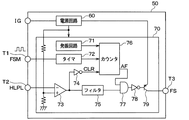
次に、フェイルセーフ部50について説明する。図2は、フェイルセーフ部50の回路図である。フェイルセーフ部50は、電源回路60およびフェイルセーフ回路70を備えている。フェイルセーフ回路70は、1つの集積回路として構成されている。フェイルセーフ回路70は、記憶部に記憶されたプログラムに従って演算処理を行うコンピュータにより構成されるものではなく、論理回路を組み合わせた組み合わせ回路、順序回路、トランジスタ等により構成されている。
Next, the fail
電源回路60は、フェイルセーフ回路70に電力を供給するフェイルセーフ用電源回路である。電源回路60は、イグニッション信号IGが入力されると、このイグニッション信号IGから所定電圧(例えば、5V)を生成する。電源回路60により生成された電圧はフェイルセーフ回路70の電源端子(図示せず)に印加される。
The
フェイルセーフ回路70は、発振回路71、タイマ72、コンパレータ73、インバータ74、78、フィルタ75、カウンタ76、AND回路77、pnp型トランジスタ79等を備えている。なお、タイマ72およびカウンタ76は、制御回路40に異常が生じているか否かを検出する異常検出部を構成している。
The fail
タイマ72には、入力端子T1から制御回路40により生成されたマイコンクロック信号FSMが入力される。タイマ52は、制御回路40より入力されたマイコンクロック信号FSMのデューティー比(マイコンクロック信号FSMの周期に対するパルス幅の比)が所定範囲内となっている場合には、このマイコンクロック信号FSMをカウンタ76へ出力する。また、制御回路40より入力されたマイコンクロック信号FSMのデューティー比が所定範囲内となっていない場合には、ローレベルの信号をカウンタ76へ出力する。つまり、このように、マイコンクロック信号FSMのデューティー比が異常となっている場合、タイマ72からカウンタ76へマイコンクロック信号FSMは出力されない。
The
コンパレータ73の反転入力端子には、入力端子T2から左側ヘッドランプ入力信号HLPLが入力される。コンパレータ73は、左側ヘッドランプ入力信号HLPLの電圧が閾値電圧以上の場合、ローレベルの信号を出力端子から出力し、左側ヘッドランプ入力信号HLPLの電圧が閾値電圧未満の場合、ハイレベルの信号を出力端子から出力する。
The left headlamp input signal HLPL is input to the inverting input terminal of the
カウンタ76は、クリア端子CLRを有し、このクリア端子CLRの電位がハイレベルなるとカウンタ76のカウント値はクリアされる。すなわち、左側ヘッドランプ入力信号HLPLの電位がハイレベルになると、カウンタ76のクリア端子CLRの電位はハイレベルとなり、カウンタ76のカウント値はクリアされる。
The
カウンタ76は、タイマ72より出力されるマイコンクロック信号FSMのパルス数を一定期間カウントし、この一定期間のマイコンクロック信号FSMのパルス数が正常範囲内となった場合には、ローレベルの信号をAND回路77へ出力する。なお、カウンタ76は、一定期間毎にカウント値をクリアして、再度、カウント動作を開始する。
The counter 76 counts the number of pulses of the microcomputer clock signal FSM output from the
また、カウンタ76は、マイコンクロック信号FSMの単位時間当たりのパルス数が正常範囲内となっていない場合には、ハイレベルの異常成立フラグAFをAND回路77へ出力する。
Further, the
フィルタ75は、ヘッドランプ入力信号HLPに含まれるノイズをカットする。フィルタ75は、ヘッドランプ入力信号HLPに含まれる高周波成分を除去し、この高周波成分を除去した信号を出力する。
The
AND回路77は、2つの入力端子と1つの出力端子を有している。AND回路77の出力端子には、インバータ78介してトランジスタ79が接続されている。
The AND circuit 77 has two input terminals and one output terminal. A
トランジスタ79のコレクタには、フェイルセーフ出力端子T3が接続されている。トランジスタ79は、オープンコレクタ出力となっている。トランジスタ79がオフすると、トランジスタ79のコレクタはハイインピーダンスとなり、トランジスタ79がオンすると、フェイルセーフ出力端子T3の電位はハイレベルとなる。
A fail safe output terminal T3 is connected to the collector of the
AND回路77の一方の入力端子にはカウンタ76の出力信号が入力され、AND回路77の他方の入力端子にはフィルタ75の出力信号が入力されている。AND回路77は、少なくとも一方の入力端子の電位がローレベルとなった場合、ローレベルの信号を出力端子から出力する。このとき、トランジスタ79のベース端子の電位はハイレベルとなり、トランジスタ79はオフする。
The output signal of the
また、AND回路77は、両方の入力端子の電位がハイレベルとなった場合、ハイレベルの信号を出力端子から出力する。このとき、トランジスタ79のベース端子の電位はローレベルとなり、トランジスタ79はオンする。
The AND circuit 77 outputs a high level signal from the output terminal when the potentials of both input terminals become high level. At this time, the potential of the base terminal of the
異常検出部72、76は、マイコンクロック信号FSMのデューティー異常、マイコンクロック信号FSMのレベルがハイレベルのままとなるハイ固着、マイコンクロック信号FSMのレベルがローレベルのままとなるロー固着、マイコンクロック信号FSMのクロック周期異常を検出する。そして、異常検出部72、76によりマイコンクロック信号FSMの異常が検出されるとカウンタ76からハイレベルの異常成立フラグAFが出力される。このとき、フィルタ75の出力信号がハイレベルであった場合、トランジスタ79はオンする。
The
また、電源回路30が異常となり制御回路40が動作を停止したときも、制御回路40からマイコンクロック信号FSMが出力されなくなるため、カウンタ76からハイレベルの異常成立フラグAFが出力される。このとき、フィルタ75の出力信号がハイレベルであった場合、トランジスタ79はオンする。
Further, when the
次に、図1〜図3を用いてフェイルセーフ回路70の作動について説明する。図3(1)に示すように、イグニッション信号IGがローレベルの状態では、電源回路60は動作しないため、フェイルセーフ回路70も動作しない。
Next, the operation of the fail
乗員の操作に応じてイグニッション信号IGがローレベルからハイレベルに変化すると、制御回路40およびフェイルセーフ回路70は動作を開始する。また、制御回路40が動作を開始すると、制御回路40からフェイルセーフ回路70へマイコンクロック信号FSMが入力される。
When the ignition signal IG changes from the low level to the high level according to the operation of the occupant, the
ここで、図3(2)に示すように、制御回路40にハイレベルの左側ヘッドランプ入力信号HLPLが入力されている場合、カウンタ76のクリア端子CLRの電位はハイレベルとなり、カウンタ76のカウント値はクリアされる。このとき、カウンタ76からローレベルの信号が出力され、トランジスタ79はオフする。また、トランジスタ79のコレクタはハイインピーダンス状態となる。
Here, as shown in FIG. 3B, when the high-level left headlamp input signal HLPL is input to the
なお、制御回路40にハイレベルの左側ヘッドランプ入力信号HLPLが入力されると、制御回路40は、第1負荷10の駆動を停止するよう第1駆動素子20を制御する。具体的には、制御回路40は、第1出力端子CNT0および第2出力端子CNT1からそれぞれローレベルの信号を出力する。
When the high-level left headlamp input signal HLPL is input to the
つまり、トランジスタ79のコレクタはハイインピーダンス状態となり、制御回路40は、第1出力端子CNT0および第2出力端子CNT1からそれぞれローレベルの信号を出力するため、第1駆動素子20のMOSFET20aのゲート端子の電位および第2駆動素子21のMOSFET21aのゲート端子の電位はそれぞれローレベルとなる。したがって、左右のヘッドランプは消灯する。
That is, the collector of the
次に、左側ヘッドランプ入力信号HLPLがハイレベルからローレベルに変化すると、カウンタ76のクリア端子CLRの電位はローレベルとなり、カウンタ76はカウント動作を開始する。このとき、マイコンクロック信号FSMが正常である場合、カウンタ76からローレベルの信号が出力される。
Next, when the left headlamp input signal HLPL changes from high level to low level, the potential of the clear terminal CLR of the
すなわち、マイコンクロック信号FSMのデューティー比が所定範囲内となっており、かつ、一定期間TFSのマイコンクロック信号FSMのパルス数が正常範囲内となっている場合、カウンタ76からローレベルの信号が出力される。このとき、フィルタ75からハイレベルの信号が出力され、トランジスタ79はオフする。また、トランジスタ79のコレクタはハイインピーダンス状態となる。
That is, the duty ratio of the microcomputer clock signal FSM has become within a predetermined range, and if the number of pulses of the microcomputer clock signal FSM for a certain period of time T FS is in the normal range, the
なお、制御回路40にローレベルの左側ヘッドランプ入力信号HLPLが入力されると、制御回路40は、第1負荷10を駆動するよう第1駆動素子20を制御する。具体的には、制御回路40は、第1出力端子CNT0からハイレベルの信号を出力するとともに、第2出力端子CNT1からハイレベルの信号を出力する。
Note that when the low-level left headlamp input signal HLPL is input to the
つまり、トランジスタ79のコレクタはハイインピーダンス状態となり、制御回路40は、第1出力端子CNT0からハイレベルの信号を出力するため、第1駆動素子20のMOSFET20aのゲート端子および第2駆動素子21のMOSFET21aのゲート端子の電位は、それぞれハイレベルとなる。したがって、左右のヘッドランプは点灯する。
That is, the collector of the
次に、マイコンクロック信号FSMが異常となり、異常検出部72、76により制御回路40および電源回路30の少なくとも一方に異常が生じていることが検出され、カウンタ76からハイレベルのフェイルセーフ信号FSが出力されると、トランジスタ79はオンする。
Next, the microcomputer clock signal FSM becomes abnormal, and it is detected by the
このように、トランジスタ79がオンすると、制御回路40の第1出力端子CNT0および第2出力端子CNT1の電位と関係なく、第1駆動素子20のMOSFET20aのゲート端子および第2駆動素子21のMOSFET21aのゲート端子の電位は、それぞれハイレベルとなる。したがって、左右のヘッドランプは点灯する。
Thus, when the
また、第1駆動素子20および第2駆動素子21は、互いに独立して第1、第2負荷10、11を駆動し、第1駆動素子20および第2駆動素子21の一方が機能しなくても他方が機能するので、夜間に左右のヘッドランプが消灯してしまうといったことを確実に防止することができる。
The
上記した構成によれば、異常検出部72、76により制御回路40および電源回路30の少なくとも一方に異常が生じていることが検出され、かつ、第1負荷10の駆動を指示する指令および第2負荷11の駆動を指示する指令の少なくとも一方が入力されている場合、フェイルセーフ回路70は、第1負荷10および第2負荷11を駆動するよう第1駆動素子20および第2駆動素子21を制御するので、負荷駆動素子を予備として備えることなく、制御回路に異常が発生した場合でも負荷を駆動することができる。さらに、車両の2つのヘッドランプをそれぞれ第1、第2の負荷とした場合、第1、第2の駆動素子の一方が故障しても他方の駆動素子がヘッドランプを駆動するため、フェイルセーフを保つことができる。
According to the configuration described above, it is detected by the
また、制御回路40は、クロック信号FSMを生成して出力し、異常検出部72、76は、制御回路40より出力されるクロック信号が正常であるか否かに基づいて制御回路40および電源回路30の少なくとも一方に異常が生じているか否かを検出するので、簡素な構成で制御回路40および電源回路30の少なくとも一方に異常が生じているか否かを検出することができる。
The
また、異常検出部72、76は、制御回路より出力されるクロック信号の電圧値、デューティー比およびクロック信号の一定期間のパルス数のいずれかが正常であるか否かに基づいて制御回路および電源回路の少なくとも一方に異常が生じているか否かを検出することができる。
Further, the
また、フェイルセーフ出力端子T3からフェイルセーフ信号が出力された場合、第1駆動素子20および第2駆動素子21は、フェイルセーフ出力端子T3より出力される信号のレベルに従って動作するので、制御回路40に異常が発生した場合でも確実に負荷を駆動することができる。
When a fail safe signal is output from the fail safe output terminal T3, the
また、フェイルセーフ出力端子T3からフェイルセーフ信号が出力されていない場合、制御回路40の第1出力端子CNT0より出力される信号で第1駆動素子20を制御するとともに、制御回路40の第2出力端子CNT1より出力される信号で第2駆動素子21を制御することができる。
When the fail safe signal is not output from the fail safe output terminal T3, the
また、フェイルセーフ回路70に電力を供給するフェイルセーフ用電源回路60を備え、フェイルセーフ回路70は、フェイルセーフ用電源回路60より供給される電力により動作するので、制御回路40および電源回路30の少なくとも一方に異常が生じた場合でも、確実に第1負荷10および第2負荷11を駆動することが可能である。
In addition, a fail-safe
また、フェイルセーフ用電源回路60は、車両から入力されるイグニッション信号IGからフェイルセーフ回路70に電力を供給するので、イグニッション信号IGがオフしたときに第1、第2負荷10、11に電流が流れない。したがって、車両に搭載されたバッテリ2のバッテリ上がりを防止することができる。
Further, since the fail-safe
車両バッテリから負荷駆動装置に供給される電圧が一時的に低下して、制御回路40にリセットがかかり制御回路40の制御による負荷の駆動が停止した場合、制御回路40の制御により第1負荷10および第2負荷11を駆動する構成では、ヘッドランプが消灯して再度点灯するまで比較的長い時間を要してしまう。しかし、本負荷駆動装置1は、組み合わせ回路、順序回路、トランジスタ等により構成されたフェイルセーフ回路70により第1負荷10および第2負荷11を駆動するので、ヘッドランプが一時的に消灯しても急点灯が可能である。
When the voltage supplied from the vehicle battery to the load driving device temporarily decreases and the
また、フェイルセーフ回路70は、第1負荷10および第2負荷11を駆動するよう第1駆動素子20および第2駆動素子21を制御するため、第1負荷10と第2負荷11の負荷電流が異なる場合でも、容易に対応することができる。
Further, since the fail
また、フェイルセーフ回路70は、回路規模が小さいため通信ドライバ等の集積回路に容易に取り込むことができ、コストを低減することが可能である。
Further, since the fail
また、フェイルセーフ回路70は、第1駆動素子20および第2駆動素子21が負荷ショート保護機能により第1、第2負荷10、11の駆動を停止した場合に、強制的に第1、第2負荷10、11を駆動するよう第1駆動素子20のMOSFET20aおよび第2駆動素子21のMOSFET21aを制御しない。したがって、負荷駆動装置の安全性を確保することができる。
Further, the fail
また、フェイルセーフ回路70は、カウンタ76を用いてマイコンクロック信号FSMの周期をモニタするため、マイコンクロック信号FSMの周期のばらつき精度を保証することができる。
Moreover, since the fail
また、フェイルセーフ回路70は、タイマ72を用いてマイコンクロック信号FSMのノイズを除去するため耐ノイズ性を向上することができる。
Further, since the fail
(他の実施形態)
(1)上記実施形態では、車両のヘッドランプを負荷として駆動するよう構成したが、例えば、車両のストップランプを負荷として駆動するよう構成してもよく、車両のヘッドランプとストップランプを負荷として駆動するよう構成してもよい。車両に搭載される上記負荷以外のものを負荷として駆動するように構成してもよい。
(Other embodiments)
(1) In the above-described embodiment, the vehicle headlamp is configured to be driven as a load. However, for example, the vehicle headlamp may be configured to be driven as a load. You may comprise so that it may drive. You may comprise so that things other than the said load mounted in a vehicle may be driven as a load.
(2)上記実施形態では、制御回路40がクロック信号(FSM)を生成して出力し、異常検出部72、76は、制御回路40より出力されるクロック信号が正常であるか否かに基づいて制御回路40および電源回路30の少なくとも一方に異常が生じているか否かを検出するようにした。
(2) In the above embodiment, the
これに対し、制御回路40が予め定められた信号パターンを生成して出力し、異常検出部72、76は、制御回路40より出力される信号パターンが予め定められた信号パターンとなっているか否かに基づいて制御回路40および電源回路30の少なくとも一方に異常が生じているか否かを検出するようにしてもよい。
In contrast, the
(3)上記実施形態では、制御回路40が1つのマイコンクロック信号FSMを生成し、異常検出部72、76が制御回路40から出力されるマイコンクロック信号FSMが正常であるか否かに基づいて制御回路40および電源回路30の少なくとも一方に異常が生じているか否かを検出するようにした。
(3) In the above embodiment, the
これに対し、制御回路40が複数のクロック信号を生成し、異常検出部72、76が制御回路40より出力される複数のクロック信号が正常であるか否かに基づいて制御回路40および電源回路30の少なくとも一方に異常が生じているか否かを検出するようにしてもよい。
In contrast, the
(4)上記実施形態では、フェイルセーフ部50に左側ヘッドランプ入力信号HLPLが入力され、右側ヘッドランプ入力信号HLPRが入力されないよう構成したが、フェイルセーフ部50に右側ヘッドランプ入力信号HLPRが入力され、左側ヘッドランプ入力信号HLPLが入力されないよう構成してもよい。
(4) In the above embodiment, the left headlamp input signal HLPL is input to the fail
(5)上記実施形態では、制御回路40に左側ヘッドランプ入力信号HLPLと右側ヘッドランプ入力信号HLPRが別々に入力されるよう構成したが、制御回路40に左右共通のヘッドランプ入力信号が入力されるよう構成してもよい。
(5) In the above embodiment, the left headlamp input signal HLPL and the right headlamp input signal HLPR are separately input to the
1 負荷駆動装置
10、11 負荷
20 第1駆動素子
21 第1駆動素子
30 電源回路
40 制御部
50 フェイルセーフ部
60 フェイルセーフ用電源回路
70 フェイルセーフ回路
DESCRIPTION OF
Claims (7)
右側ヘッドランプを第2負荷(11)として駆動する第2駆動素子(21)を独立に配置し、
前記第1負荷の駆動を指示する指令および前記第2負荷の駆動を指示する指令の入力に応じて前記第1駆動素子および前記第2駆動素子を制御する制御回路(40)と、
前記制御回路に電力を供給する電源回路(30)と、を備えた負荷駆動装置であって、
前記制御回路および前記電源回路の少なくとも一方に異常が生じているか否かを検出する異常検出部(72、76)を有し、該異常検出部により前記制御回路および前記電源回路の少なくとも一方に異常が生じていることが検出され、かつ、前記第1負荷の駆動を指示する指令および前記第2負荷の駆動を指示する指令の少なくとも一方が入力されている場合、前記第1負荷および前記第2負荷を駆動するよう前記第1駆動素子および前記第2駆動素子を制御するフェイルセーフ回路(70)を備えた負荷駆動装置。 A first drive element (20) for driving the left headlamp as a first load (10);
Second place independently driving element (21) for driving the right headlamp as a second load (11),
A control circuit (40) for controlling the first drive element and the second drive element in response to an instruction for instructing driving of the first load and an instruction for instructing driving of the second load;
A power supply circuit (30) for supplying power to the control circuit,
An abnormality detection unit (72, 76) that detects whether or not an abnormality has occurred in at least one of the control circuit and the power supply circuit, and an abnormality has occurred in at least one of the control circuit and the power supply circuit by the abnormality detection unit. Is detected, and at least one of a command for instructing driving of the first load and a command for instructing driving of the second load is input, the first load and the second A load driving device comprising a fail safe circuit (70) for controlling the first driving element and the second driving element so as to drive a load.
前記異常検出部は、前記制御回路より出力される前記クロック信号が正常であるか否かに基づいて前記制御回路および前記電源回路の少なくとも一方に異常が生じているか否かを検出する請求項1に記載の負荷駆動装置。 The control circuit generates and outputs a clock signal (FSM),
The abnormality detection unit detects whether or not an abnormality has occurred in at least one of the control circuit and the power supply circuit based on whether or not the clock signal output from the control circuit is normal. The load drive device described in 1.
前記フェイルセーフ回路は、前記異常検出部により前記制御回路および前記電源回路の少なくとも一方に異常が生じていることが検出され、かつ、前記第1負荷の駆動を指示する指令および前記第2負荷の駆動を指示する指令の少なくとも一方が入力されている場合、前記第1負荷および前記第2負荷を駆動するよう前記第1駆動素子および前記第2駆動素子を制御するフェイルセーフ信号(FS)を出力するフェイルセーフ出力端子(T3)を有し、
前記フェイルセーフ出力端子は、前記第1出力端子および前記第2出力端子と互いに接続されており、
前記フェイルセーフ出力端子から前記フェイルセーフ信号が出力された場合、前記第1駆動素子および前記第2駆動素子は、前記フェイルセーフ出力端子より出力される信号のレベルに従って動作する請求項1ないし3のいずれか1つに記載の負荷駆動装置。 The control circuit has a first output terminal (CNT0) for outputting a signal for controlling the first drive element and a second output terminal (CNT1) for outputting a signal for controlling the second drive element,
The fail safe circuit detects that an abnormality has occurred in at least one of the control circuit and the power supply circuit by the abnormality detection unit, and a command for instructing driving of the first load and the second load When at least one of commands instructing driving is input, a fail safe signal (FS) for controlling the first driving element and the second driving element is output so as to drive the first load and the second load. A fail-safe output terminal (T3)
The fail safe output terminal is connected to the first output terminal and the second output terminal,
4. The first drive element and the second drive element operate according to a level of a signal output from the fail-safe output terminal when the fail-safe signal is output from the fail-safe output terminal. The load drive apparatus as described in any one.
前記フェイルセーフ回路は、前記フェイルセーフ用電源回路より供給される電力により動作する請求項1ないし5のいずれか1つに記載の負荷駆動装置。 A fail-safe power supply circuit (60) for supplying power to the fail-safe circuit;
The load driving device according to any one of claims 1 to 5, wherein the fail-safe circuit is operated by electric power supplied from the fail-safe power supply circuit.
Priority Applications (2)
| Application Number | Priority Date | Filing Date | Title |
|---|---|---|---|
| JP2016005286A JP6414088B2 (en) | 2016-01-14 | 2016-01-14 | Load drive device |
| US15/399,786 US10262822B2 (en) | 2016-01-14 | 2017-01-06 | Load drive apparatus |
Applications Claiming Priority (1)
| Application Number | Priority Date | Filing Date | Title |
|---|---|---|---|
| JP2016005286A JP6414088B2 (en) | 2016-01-14 | 2016-01-14 | Load drive device |
Publications (2)
| Publication Number | Publication Date |
|---|---|
| JP2017124748A JP2017124748A (en) | 2017-07-20 |
| JP6414088B2 true JP6414088B2 (en) | 2018-10-31 |
Family
ID=59314926
Family Applications (1)
| Application Number | Title | Priority Date | Filing Date |
|---|---|---|---|
| JP2016005286A Active JP6414088B2 (en) | 2016-01-14 | 2016-01-14 | Load drive device |
Country Status (2)
| Country | Link |
|---|---|
| US (1) | US10262822B2 (en) |
| JP (1) | JP6414088B2 (en) |
Families Citing this family (3)
| Publication number | Priority date | Publication date | Assignee | Title |
|---|---|---|---|---|
| US10666257B1 (en) | 2018-11-02 | 2020-05-26 | Texas Instruments Incorporated | Failsafe, ultra-wide voltage input output interface using low-voltage gate oxide transistors |
| US10673436B1 (en) * | 2018-11-30 | 2020-06-02 | Texas Instruments Incorporated | Failsafe device |
| WO2023010250A1 (en) * | 2021-08-02 | 2023-02-09 | 华为技术有限公司 | Control apparatus, electronic control system, and vehicle |
Family Cites Families (11)
| Publication number | Priority date | Publication date | Assignee | Title |
|---|---|---|---|---|
| JP4094827B2 (en) * | 2001-05-29 | 2008-06-04 | 矢崎総業株式会社 | Drive control device |
| DE10325363A1 (en) * | 2003-05-23 | 2005-01-13 | Pilz Gmbh & Co. | Safety switching device for fail-safe disconnection of an electrical consumer and corresponding method |
| JP4561715B2 (en) * | 2006-09-21 | 2010-10-13 | 住友電装株式会社 | Headlamp control circuit |
| JP4776596B2 (en) | 2007-08-01 | 2011-09-21 | 株式会社小糸製作所 | Lighting control device for vehicle lamp |
| JP2010018170A (en) * | 2008-07-10 | 2010-01-28 | Denso Corp | Vehicular auto-light device |
| US9013105B2 (en) * | 2009-09-10 | 2015-04-21 | Mitsubishi Electric Corporation | Headlamp light source lighting device and vehicle headlamp lighting system |
| JP5267425B2 (en) * | 2009-11-04 | 2013-08-21 | アンデン株式会社 | Load drive device having fail-safe function |
| JP2011213289A (en) * | 2010-04-01 | 2011-10-27 | Denso Corp | Vehicle hazard control system and vehicle hazard control device |
| JP5483475B2 (en) * | 2011-09-13 | 2014-05-07 | オムロンオートモーティブエレクトロニクス株式会社 | Load control device |
| JP5586554B2 (en) | 2011-09-28 | 2014-09-10 | オムロンオートモーティブエレクトロニクス株式会社 | Load control device |
| US9517715B1 (en) * | 2015-12-20 | 2016-12-13 | Toyota Motor Engineering & Manufacturing North America, Inc. | Light driver arrangements for vehicle headlamps |
-
2016
- 2016-01-14 JP JP2016005286A patent/JP6414088B2/en active Active
-
2017
- 2017-01-06 US US15/399,786 patent/US10262822B2/en active Active
Also Published As
| Publication number | Publication date |
|---|---|
| JP2017124748A (en) | 2017-07-20 |
| US10262822B2 (en) | 2019-04-16 |
| US20170207050A1 (en) | 2017-07-20 |
Similar Documents
| Publication | Publication Date | Title |
|---|---|---|
| JP6199721B2 (en) | Vehicle lighting | |
| JP6414088B2 (en) | Load drive device | |
| EP2881286B1 (en) | Direction-indication device | |
| JP2006103404A (en) | Lighting control circuit of vehicle lamp | |
| JP6390916B2 (en) | Anomaly detection device | |
| JP5037414B2 (en) | Power supply control device | |
| JP6762419B2 (en) | Load drive | |
| JP6240587B2 (en) | Disconnection detection device and disconnection detection method | |
| JP4318300B2 (en) | Lighting control device and failure detection device | |
| JP2019097124A (en) | Load drive circuit | |
| JP2008276727A (en) | Load drive system | |
| JP6416718B2 (en) | Fail-safe circuit | |
| JP4725492B2 (en) | Load control device and load control method | |
| EP3264864B1 (en) | Led drive circuit | |
| JP7421958B2 (en) | drive device | |
| JP2014216765A (en) | Led anomaly detection device | |
| JP5904375B2 (en) | Power supply control device | |
| JP2009266723A (en) | Lighting control device | |
| JP4415655B2 (en) | Vehicle lamp control device | |
| KR100672258B1 (en) | Turn signal lamp fail sensing device | |
| JP2010129258A (en) | Lamp tool for vehicle | |
| JP2009159697A (en) | Motor control device | |
| KR20200069677A (en) | Apparatus for driving warning light and method for driving the same | |
| JP6666776B2 (en) | Error protection circuit | |
| KR101903970B1 (en) | Tell-Tale Circuit of LED Lamp in Vehicle |
Legal Events
| Date | Code | Title | Description |
|---|---|---|---|
| A977 | Report on retrieval |
Free format text: JAPANESE INTERMEDIATE CODE: A971007 Effective date: 20171122 |
|
| A131 | Notification of reasons for refusal |
Free format text: JAPANESE INTERMEDIATE CODE: A131 Effective date: 20171128 |
|
| A521 | Request for written amendment filed |
Free format text: JAPANESE INTERMEDIATE CODE: A523 Effective date: 20180126 |
|
| A131 | Notification of reasons for refusal |
Free format text: JAPANESE INTERMEDIATE CODE: A131 Effective date: 20180424 |
|
| A521 | Request for written amendment filed |
Free format text: JAPANESE INTERMEDIATE CODE: A523 Effective date: 20180620 |
|
| TRDD | Decision of grant or rejection written | ||
| A01 | Written decision to grant a patent or to grant a registration (utility model) |
Free format text: JAPANESE INTERMEDIATE CODE: A01 Effective date: 20180904 |
|
| A61 | First payment of annual fees (during grant procedure) |
Free format text: JAPANESE INTERMEDIATE CODE: A61 Effective date: 20180917 |
|
| R150 | Certificate of patent or registration of utility model |
Ref document number: 6414088 Country of ref document: JP Free format text: JAPANESE INTERMEDIATE CODE: R150 |
|
| S533 | Written request for registration of change of name |
Free format text: JAPANESE INTERMEDIATE CODE: R313533 |
|
| R350 | Written notification of registration of transfer |
Free format text: JAPANESE INTERMEDIATE CODE: R350 |
|
| R250 | Receipt of annual fees |
Free format text: JAPANESE INTERMEDIATE CODE: R250 |
|
| R250 | Receipt of annual fees |
Free format text: JAPANESE INTERMEDIATE CODE: R250 |
|
| R250 | Receipt of annual fees |
Free format text: JAPANESE INTERMEDIATE CODE: R250 |