JP6400845B2 - Elastic electrical contact terminal with improved environmental resistance and method for manufacturing the same - Google Patents
Elastic electrical contact terminal with improved environmental resistance and method for manufacturing the same Download PDFInfo
- Publication number
- JP6400845B2 JP6400845B2 JP2017516940A JP2017516940A JP6400845B2 JP 6400845 B2 JP6400845 B2 JP 6400845B2 JP 2017516940 A JP2017516940 A JP 2017516940A JP 2017516940 A JP2017516940 A JP 2017516940A JP 6400845 B2 JP6400845 B2 JP 6400845B2
- Authority
- JP
- Japan
- Prior art keywords
- contact terminal
- electrical contact
- polymer film
- copper foil
- elastic
- Prior art date
- Legal status (The legal status is an assumption and is not a legal conclusion. Google has not performed a legal analysis and makes no representation as to the accuracy of the status listed.)
- Active
Links
Images


Classifications
-
- H—ELECTRICITY
- H01—ELECTRIC ELEMENTS
- H01R—ELECTRICALLY-CONDUCTIVE CONNECTIONS; STRUCTURAL ASSOCIATIONS OF A PLURALITY OF MUTUALLY-INSULATED ELECTRICAL CONNECTING ELEMENTS; COUPLING DEVICES; CURRENT COLLECTORS
- H01R4/00—Electrically-conductive connections between two or more conductive members in direct contact, i.e. touching one another; Means for effecting or maintaining such contact; Electrically-conductive connections having two or more spaced connecting locations for conductors and using contact members penetrating insulation
- H01R4/58—Electrically-conductive connections between two or more conductive members in direct contact, i.e. touching one another; Means for effecting or maintaining such contact; Electrically-conductive connections having two or more spaced connecting locations for conductors and using contact members penetrating insulation characterised by the form or material of the contacting members
- H01R4/62—Connections between conductors of different materials; Connections between or with aluminium or steel-core aluminium conductors
- H01R4/625—Soldered or welded connections
-
- H—ELECTRICITY
- H01—ELECTRIC ELEMENTS
- H01R—ELECTRICALLY-CONDUCTIVE CONNECTIONS; STRUCTURAL ASSOCIATIONS OF A PLURALITY OF MUTUALLY-INSULATED ELECTRICAL CONNECTING ELEMENTS; COUPLING DEVICES; CURRENT COLLECTORS
- H01R4/00—Electrically-conductive connections between two or more conductive members in direct contact, i.e. touching one another; Means for effecting or maintaining such contact; Electrically-conductive connections having two or more spaced connecting locations for conductors and using contact members penetrating insulation
- H01R4/58—Electrically-conductive connections between two or more conductive members in direct contact, i.e. touching one another; Means for effecting or maintaining such contact; Electrically-conductive connections having two or more spaced connecting locations for conductors and using contact members penetrating insulation characterised by the form or material of the contacting members
-
- H—ELECTRICITY
- H01—ELECTRIC ELEMENTS
- H01R—ELECTRICALLY-CONDUCTIVE CONNECTIONS; STRUCTURAL ASSOCIATIONS OF A PLURALITY OF MUTUALLY-INSULATED ELECTRICAL CONNECTING ELEMENTS; COUPLING DEVICES; CURRENT COLLECTORS
- H01R11/00—Individual connecting elements providing two or more spaced connecting locations for conductive members which are, or may be, thereby interconnected, e.g. end pieces for wires or cables supported by the wire or cable and having means for facilitating electrical connection to some other wire, terminal, or conductive member, blocks of binding posts
- H01R11/01—Individual connecting elements providing two or more spaced connecting locations for conductive members which are, or may be, thereby interconnected, e.g. end pieces for wires or cables supported by the wire or cable and having means for facilitating electrical connection to some other wire, terminal, or conductive member, blocks of binding posts characterised by the form or arrangement of the conductive interconnection between the connecting locations
-
- H—ELECTRICITY
- H01—ELECTRIC ELEMENTS
- H01R—ELECTRICALLY-CONDUCTIVE CONNECTIONS; STRUCTURAL ASSOCIATIONS OF A PLURALITY OF MUTUALLY-INSULATED ELECTRICAL CONNECTING ELEMENTS; COUPLING DEVICES; CURRENT COLLECTORS
- H01R12/00—Structural associations of a plurality of mutually-insulated electrical connecting elements, specially adapted for printed circuits, e.g. printed circuit boards [PCB], flat or ribbon cables, or like generally planar structures, e.g. terminal strips, terminal blocks; Coupling devices specially adapted for printed circuits, flat or ribbon cables, or like generally planar structures; Terminals specially adapted for contact with, or insertion into, printed circuits, flat or ribbon cables, or like generally planar structures
- H01R12/50—Fixed connections
- H01R12/51—Fixed connections for rigid printed circuits or like structures
- H01R12/55—Fixed connections for rigid printed circuits or like structures characterised by the terminals
- H01R12/57—Fixed connections for rigid printed circuits or like structures characterised by the terminals surface mounting terminals
-
- H—ELECTRICITY
- H01—ELECTRIC ELEMENTS
- H01R—ELECTRICALLY-CONDUCTIVE CONNECTIONS; STRUCTURAL ASSOCIATIONS OF A PLURALITY OF MUTUALLY-INSULATED ELECTRICAL CONNECTING ELEMENTS; COUPLING DEVICES; CURRENT COLLECTORS
- H01R13/00—Details of coupling devices of the kinds covered by groups H01R12/70 or H01R24/00 - H01R33/00
- H01R13/02—Contact members
- H01R13/22—Contacts for co-operating by abutting
- H01R13/24—Contacts for co-operating by abutting resilient; resiliently-mounted
-
- H—ELECTRICITY
- H01—ELECTRIC ELEMENTS
- H01R—ELECTRICALLY-CONDUCTIVE CONNECTIONS; STRUCTURAL ASSOCIATIONS OF A PLURALITY OF MUTUALLY-INSULATED ELECTRICAL CONNECTING ELEMENTS; COUPLING DEVICES; CURRENT COLLECTORS
- H01R13/00—Details of coupling devices of the kinds covered by groups H01R12/70 or H01R24/00 - H01R33/00
- H01R13/648—Protective earth or shield arrangements on coupling devices, e.g. anti-static shielding
- H01R13/658—High frequency shielding arrangements, e.g. against EMI [Electro-Magnetic Interference] or EMP [Electro-Magnetic Pulse]
- H01R13/6581—Shield structure
- H01R13/6582—Shield structure with resilient means for engaging mating connector
- H01R13/6583—Shield structure with resilient means for engaging mating connector with separate conductive resilient members between mating shield members
- H01R13/6584—Shield structure with resilient means for engaging mating connector with separate conductive resilient members between mating shield members formed by conductive elastomeric members, e.g. flat gaskets or O-rings
-
- H—ELECTRICITY
- H01—ELECTRIC ELEMENTS
- H01R—ELECTRICALLY-CONDUCTIVE CONNECTIONS; STRUCTURAL ASSOCIATIONS OF A PLURALITY OF MUTUALLY-INSULATED ELECTRICAL CONNECTING ELEMENTS; COUPLING DEVICES; CURRENT COLLECTORS
- H01R43/00—Apparatus or processes specially adapted for manufacturing, assembling, maintaining, or repairing of line connectors or current collectors or for joining electric conductors
- H01R43/007—Apparatus or processes specially adapted for manufacturing, assembling, maintaining, or repairing of line connectors or current collectors or for joining electric conductors for elastomeric connecting elements
-
- H—ELECTRICITY
- H05—ELECTRIC TECHNIQUES NOT OTHERWISE PROVIDED FOR
- H05K—PRINTED CIRCUITS; CASINGS OR CONSTRUCTIONAL DETAILS OF ELECTRIC APPARATUS; MANUFACTURE OF ASSEMBLAGES OF ELECTRICAL COMPONENTS
- H05K1/00—Printed circuits
- H05K1/02—Details
- H05K1/11—Printed elements for providing electric connections to or between printed circuits
-
- H—ELECTRICITY
- H05—ELECTRIC TECHNIQUES NOT OTHERWISE PROVIDED FOR
- H05K—PRINTED CIRCUITS; CASINGS OR CONSTRUCTIONAL DETAILS OF ELECTRIC APPARATUS; MANUFACTURE OF ASSEMBLAGES OF ELECTRICAL COMPONENTS
- H05K3/00—Apparatus or processes for manufacturing printed circuits
- H05K3/30—Assembling printed circuits with electric components, e.g. with resistor
- H05K3/32—Assembling printed circuits with electric components, e.g. with resistor electrically connecting electric components or wires to printed circuits
- H05K3/34—Assembling printed circuits with electric components, e.g. with resistor electrically connecting electric components or wires to printed circuits by soldering
-
- H—ELECTRICITY
- H01—ELECTRIC ELEMENTS
- H01R—ELECTRICALLY-CONDUCTIVE CONNECTIONS; STRUCTURAL ASSOCIATIONS OF A PLURALITY OF MUTUALLY-INSULATED ELECTRICAL CONNECTING ELEMENTS; COUPLING DEVICES; CURRENT COLLECTORS
- H01R13/00—Details of coupling devices of the kinds covered by groups H01R12/70 or H01R24/00 - H01R33/00
- H01R13/02—Contact members
- H01R13/22—Contacts for co-operating by abutting
- H01R13/24—Contacts for co-operating by abutting resilient; resiliently-mounted
- H01R13/2407—Contacts for co-operating by abutting resilient; resiliently-mounted characterized by the resilient means
- H01R13/2414—Contacts for co-operating by abutting resilient; resiliently-mounted characterized by the resilient means conductive elastomers
-
- H—ELECTRICITY
- H05—ELECTRIC TECHNIQUES NOT OTHERWISE PROVIDED FOR
- H05K—PRINTED CIRCUITS; CASINGS OR CONSTRUCTIONAL DETAILS OF ELECTRIC APPARATUS; MANUFACTURE OF ASSEMBLAGES OF ELECTRICAL COMPONENTS
- H05K2201/00—Indexing scheme relating to printed circuits covered by H05K1/00
- H05K2201/10—Details of components or other objects attached to or integrated in a printed circuit board
- H05K2201/10227—Other objects, e.g. metallic pieces
- H05K2201/1031—Surface mounted metallic connector elements
-
- H—ELECTRICITY
- H05—ELECTRIC TECHNIQUES NOT OTHERWISE PROVIDED FOR
- H05K—PRINTED CIRCUITS; CASINGS OR CONSTRUCTIONAL DETAILS OF ELECTRIC APPARATUS; MANUFACTURE OF ASSEMBLAGES OF ELECTRICAL COMPONENTS
- H05K3/00—Apparatus or processes for manufacturing printed circuits
- H05K3/30—Assembling printed circuits with electric components, e.g. with resistor
- H05K3/32—Assembling printed circuits with electric components, e.g. with resistor electrically connecting electric components or wires to printed circuits
- H05K3/34—Assembling printed circuits with electric components, e.g. with resistor electrically connecting electric components or wires to printed circuits by soldering
- H05K3/341—Surface mounted components
- H05K3/3431—Leadless components
-
- Y—GENERAL TAGGING OF NEW TECHNOLOGICAL DEVELOPMENTS; GENERAL TAGGING OF CROSS-SECTIONAL TECHNOLOGIES SPANNING OVER SEVERAL SECTIONS OF THE IPC; TECHNICAL SUBJECTS COVERED BY FORMER USPC CROSS-REFERENCE ART COLLECTIONS [XRACs] AND DIGESTS
- Y02—TECHNOLOGIES OR APPLICATIONS FOR MITIGATION OR ADAPTATION AGAINST CLIMATE CHANGE
- Y02P—CLIMATE CHANGE MITIGATION TECHNOLOGIES IN THE PRODUCTION OR PROCESSING OF GOODS
- Y02P70/00—Climate change mitigation technologies in the production process for final industrial or consumer products
- Y02P70/50—Manufacturing or production processes characterised by the final manufactured product
Description
本発明は弾性電気接触端子に関するものであり、特に、腐食しにくく、耐環境性が向上され、はんだ付けの強度の信頼性がよく向上された弾性電気接触端子に関する。 The present invention relates to an elastic electrical contact terminal, and more particularly, to an elastic electrical contact terminal that is not easily corroded, has improved environmental resistance, and has improved soldering strength reliability.
一般に、はんだ付け(soldering)が可能な弾性接触端子は、電気伝導度がよく、弾性回復力が優秀で、はんだ付け温度に耐えられることが要求される。 In general, an elastic contact terminal that can be soldered is required to have good electrical conductivity, excellent elastic recovery, and withstand the soldering temperature.
弾性電気接触端子の例として、本発明者による特許文献1は、一定体積を有する絶縁発泡ゴムと、前記絶縁発泡ゴムを包みながら接触される絶縁非発泡接着剤層と、一面が前記絶縁非発泡接着剤層を包むように前記絶縁非発泡層に接着され、他面に金属層が一体に形成された耐熱ポリマーフィルムと、を含むことを特徴とするはんだ付け可能な弾性電気接触端子を開示する。 As an example of the elastic electrical contact terminal, Patent Document 1 by the present inventor discloses an insulating foam rubber having a certain volume, an insulating non-foamed adhesive layer that is contacted while wrapping the insulating foam rubber, and one surface of the insulating non-foaming surface. A solderable elastic electrical contact terminal comprising: a heat-resistant polymer film bonded to the insulating non-foamed layer so as to wrap an adhesive layer and having a metal layer integrally formed on the other surface.
また、特許文献2は、内部に長さ方向に貫通孔が形成された絶縁弾性耐熱ゴムコアと、前記絶縁弾性耐熱ゴムコアを包むように接着される絶縁耐熱接着剤層と、一面が前記絶縁耐熱接着剤層を包むように前記絶縁耐熱接着剤層に接着されて、他の面に金属層が一体に形成された耐熱ポリマーフィルムと、を含むが、前記ポリマーフィルムは両端が離隔されるように前記耐熱接着剤層に接着され、前記絶縁弾性耐熱ゴムコアの下面は、幅方向の両端から中間部分に向かって凹む形状に傾斜して形成されることを特徴とするリフローはんだ付けが可能な弾性電気接触端子を開示する。 Patent Document 2 discloses an insulating elastic heat resistant rubber core having a through hole formed in the length direction therein, an insulating heat resistant adhesive layer bonded so as to wrap the insulating elastic heat resistant rubber core, and one surface of the insulating heat resistant adhesive. A heat-resistant polymer film that is adhered to the insulating heat-resistant adhesive layer so as to wrap the layer and a metal layer is integrally formed on the other surface, and the polymer film has the heat-resistant adhesion so that both ends are separated from each other. An elastic electrical contact terminal capable of reflow soldering, characterized in that the lower surface of the insulating elastic heat resistant rubber core is bonded to the agent layer, and is inclined so as to be recessed from both ends in the width direction toward the middle portion. Disclose.
前記のような電気接触端子を製造する過程では、ロール(Roll)状のシリコンゴムを用意し、シリコンゴムの上に長さ方向に液状のシリコンゴム接着剤を連続して介在させ、液状のシリコンゴム接着剤の上に金属層が形成されたポリマーフィルムを金属層が外部に露出するように包んだ後、シリコンゴム接着剤を硬化させてポリマーフィルムを接着し、一定長さ、例えば500mmに切断し、次に顧客の必要な長さ、例えば3mmに切断した後、金属がめっきされた製品をリールテーピングする。 In the process of manufacturing the electrical contact terminal as described above, a roll-shaped silicon rubber is prepared, and a liquid silicon rubber adhesive is continuously disposed on the silicon rubber in the length direction to form liquid silicon. After wrapping the polymer film with the metal layer on the rubber adhesive so that the metal layer is exposed to the outside, the silicone rubber adhesive is cured to adhere the polymer film and cut to a certain length, for example 500mm Then, after cutting to a length required by the customer, for example, 3 mm, the product plated with metal is reel-taped.
ここで、金属層は銅箔の上に錫や銀がめっきされるか、ニッケルめっきの後、その上に錫または金をめっきして形成される。銅箔の厚さは略0.01mmであって、錫、ニッケルまたは金の厚さより相当厚い。 Here, the metal layer is formed by plating tin or silver on a copper foil, or plating nickel or gold on the copper foil. The thickness of the copper foil is about 0.01 mm, which is considerably thicker than the thickness of tin, nickel or gold.
このように、従来の接触端子の銅箔の上には、取り付けられることが防止されてはんだクリームによるはんだ付けがよくできるように耐環境性が銅より優れた金属めっき層が形成されるが、接触端子を製造する過程で顧客の望む長さに切断するため、接触端子の長さ方向の側面に形成される切断面には銅箔が外部に露出してしまう。 Thus, on the copper foil of the conventional contact terminal, a metal plating layer having an environment resistance superior to that of copper is formed so that it can be prevented from being attached and soldering with a solder cream can be performed well. Since the contact terminal is cut to a length desired by the customer in the process of manufacturing the contact terminal, the copper foil is exposed to the outside on the cut surface formed on the side surface in the length direction of the contact terminal.
言い換えると、従来の接触端子では、錫などの金属層がめっきされた銅箔を有するポリマーフィルムをコアに包んだ後、切断して製造していたため、切断面では当然銅箔が外部に露出されてしまっていた。 In other words, in conventional contact terminals, a polymer film having a copper foil plated with a metal layer such as tin is wrapped in a core and then cut, so that the copper foil is naturally exposed to the outside at the cut surface. It was.
その結果、塩水テストのような信頼性テストにおいて、外部に露出された銅箔に塩水が接触することで塩水による腐食のため塩水テストに通らなくなるか、使用中に外部に露出した銅箔に錆がよく付着し、品質低下をもたらす。 As a result, in reliability tests such as the salt water test, salt water does not pass the salt water test due to salt water corrosion due to contact with the copper foil exposed to the outside, or the copper foil exposed outside during use is rusted. Adheres well and causes quality degradation.
また、接触端子をリフローはんだ付けして回路基板に実装する場合、外部に露出した切断面では銅箔が露出するため銅箔では金属めっき層に比べ鉛上がり現象が少なく発生し、結果的に切断面のはんだ付けの強度が弱くなる短所がある。 Also, when reflow soldering the contact terminals and mounting them on the circuit board, the copper foil is exposed on the cut surface exposed to the outside, so there is less lead rise in the copper foil than the metal plating layer, resulting in cutting There is a disadvantage that the soldering strength of the surface is weakened.
また、ポリマーフィルムを包みながら接着される銅箔はコアの下面両端から曲げられるため、曲げられた銅箔はその大きさは小さいが常に元の位置に復帰しようとする弾性復元力を受けている。これと共に、接触端子をリフローはんだ付けで回路基板に実装する場合、溶融されたはんだクリームが銅箔に作用し、銅箔を下方に引っ張りながら銅箔自体の弾性復元力にこの力を加えるため、ポリマーフィルムの両端がコアまたは接着剤から剥離されて毛羽立つ恐れがある問題がある。 Also, since the copper foil that is bonded while wrapping the polymer film is bent from both ends of the lower surface of the core, the bent copper foil is subjected to an elastic restoring force that always tries to return to its original position, although its size is small . At the same time, when the contact terminals are mounted on the circuit board by reflow soldering, the melted solder cream acts on the copper foil, and this force is applied to the elastic restoring force of the copper foil itself while pulling the copper foil downward. There is a problem that both ends of the polymer film may be peeled off from the core or the adhesive and become fuzzy.
同じく、製造工程中にポリマーフィルムとコアを接着剤で接着する際、接着が完全に行われる前に、前述のような原理によってポリマーフィルムの両端部がコアまたは接着剤から剥離する確率が大きい問題点がある。 Similarly, when the polymer film and the core are bonded with an adhesive during the manufacturing process, there is a high probability that both ends of the polymer film will peel off from the core or the adhesive according to the principle described above before the bonding is completely performed. There is a point.
よって、本発明の目的は、腐食に強い弾性電気接触端子を提供することである。 Accordingly, an object of the present invention is to provide an elastic electrical contact terminal that is resistant to corrosion.
また、本発明の他の目的は、はんだ付けの強度や信頼性を向上させた弾性電気接触端子を提供することにある。 Another object of the present invention is to provide an elastic electrical contact terminal with improved soldering strength and reliability.
本発明のまた他の目的は、側方向から印加される外部の力に強く対向することができるはんだ付けの強度を有する弾性電気接触端子を提供することである。 Another object of the present invention is to provide an elastic electric contact terminal having a soldering strength capable of strongly opposing an external force applied from the side direction.
本発明の更に他の目的は、製造工程中やはんだ付けの後、ポリマーフィルムの両端が剥離することを最小化することができる弾性電気接触端子を提供することである。 Still another object of the present invention is to provide an elastic electrical contact terminal capable of minimizing peeling of both ends of the polymer film during the manufacturing process or after soldering.
前記目的は、弾性コア、接着剤層を介在して前記コアを包みながら接着されるポリマーフィルム、及び前記ポリマーフィルムを包みながら接着されるはんだ付けが可能な銅箔を含み、前記銅箔が外部に露出される全ての面に金属めっき層が形成されることを特徴とする弾性電気接触端子によって達成される。 The object includes an elastic core, a polymer film bonded while wrapping the core with an adhesive layer interposed therebetween, and a solderable copper foil that is bonded while wrapping the polymer film, the copper foil being external This is achieved by an elastic electrical contact terminal characterized in that a metal plating layer is formed on all surfaces exposed to the surface.
好ましくは、前記電気接触端子の比重は水の比重より小さく、前記電気接触端子は幅が長さより大きい。 Preferably, the specific gravity of the electric contact terminal is smaller than the specific gravity of water, and the width of the electric contact terminal is larger than the length.
好ましくは、前記金属めっき層は、錫(Sn)や銀(Ag)をめっきして形成されるか、ニッケル(Ni)めっきの後、錫や金(Au)をめっきして形成されてもよく、銅箔より腐食性が小さい。 Preferably, the metal plating layer may be formed by plating tin (Sn) or silver (Ag), or may be formed by plating tin or gold (Au) after nickel (Ni) plating. Less corrosive than copper foil.
好ましくは、前記銅箔の厚さが前記金属めっき層の厚さより厚くてもよく、前記銅箔は電解銅箔または圧延銅箔であって、前記銅箔の上に前記ポリマーフィルムに対応する液状のポリマーを塗布し硬化して接着される。 Preferably, the thickness of the copper foil may be larger than the thickness of the metal plating layer, and the copper foil is an electrolytic copper foil or a rolled copper foil, and a liquid corresponding to the polymer film on the copper foil. The polymer is applied and cured to be bonded.
好ましくは、はんだ付けの際、前記金属めっき層は前記銅箔よりはんだ付けを容易に行うことができる。 Preferably, at the time of soldering, the metal plating layer can be soldered more easily than the copper foil.
好ましくは、前記弾性コアはチューブ状または発泡状のシリコンゴムであり、前記接着剤はシリコンゴム接着剤であって、前記ポリマーフィルムはポリイミド(IP)である。 Preferably, the elastic core is tube-shaped or foamed silicon rubber, the adhesive is a silicon rubber adhesive, and the polymer film is polyimide (IP).
好ましくは、前記金属めっき層は無電解めっきで形成され、表面粗さが増加することではんだ付けの強度が向上する。 Preferably, the metal plating layer is formed by electroless plating, and the strength of soldering is improved by increasing the surface roughness.
好ましくは、前記電気接触端子は回路基板の導電パターンにはんだクリームによってはんだ付けされ、対向する電気伝導性対象物と弾性を有して電気的に連結する。 Preferably, the electrical contact terminal is soldered to the conductive pattern of the circuit board with a solder cream, and is electrically connected to the opposing electrically conductive object with elasticity.
好ましくは、前記コアの下面において、前記ポリマーフィルムの両端から一定部分だけ前記金属層が除去されて前記ポリマーフィルムが外部に露出されてもよく、前記一定部分は前記金属層を露光及びエッチングして形成される。 Preferably, on the lower surface of the core, the metal layer may be removed from the both ends of the polymer film to expose the polymer film to the outside, and the constant portion may be exposed and etched to the metal layer. It is formed.
好ましくは、前記コアの下面において、前記ポリマーフィルムの両端から幅方向に一定幅だけ、そして長さ方向に連続して前記金属層が除去される。 Preferably, on the lower surface of the core, the metal layer is removed from both ends of the polymer film by a certain width in the width direction and continuously in the length direction.
好ましくは、前記コアは、その上面から下方に一定な幅と深さで凹んで形成され、長さ方向に沿って延長する少なくとも一つ以上のチャネル(channel)を備える。 Preferably, the core includes at least one channel that is formed to be recessed downward with a constant width and depth from an upper surface thereof and extends along a length direction.
好ましくは、前記ポリマーフィルムは前記チャネルを横切って前記両側壁の上にかけられるか前記コアの外面に密着して接着され、前記チャネルの両側壁が前記対象物を弾性的に支持する。 Preferably, the polymer film is placed on the both side walls across the channel or in close contact with the outer surface of the core, and the both side walls of the channel elastically support the object.
好ましくは、前記チャネルは多数個形成され、前記チャネルの間に前記両側壁に対応する高さで突出され、前記長さ方向に延長された支持壁を更に含む。 Preferably, a plurality of the channels are formed, and further include support walls protruding at a height corresponding to the side walls between the channels and extending in the length direction.
好ましくは、前記支持壁の上面は前記接着剤層を介在して前記ポリマーフィルムに接着される。 Preferably, the upper surface of the support wall is bonded to the polymer film via the adhesive layer.
好ましくは、前記両側壁の前記チャネル側の側面は傾斜を成し、前記対象物による加圧の際、前記両側壁が前記チャネル側に傾く。 Preferably, the side surface of the both side walls on the channel side is inclined, and the both side walls are inclined toward the channel side when being pressed by the object.
前記目的は、弾性コア、接着剤層を介在して前記コアを包みながら接着されるポリマーフィルム、及び前記ポリマーフィルムを包みながら接着されるはんだ付けが可能な金属層を含み、前記金属層は、前記ポリマーフィルムの上に金属シード(seed)をスパッタリングした後、その上にめっきによって形成される銅めっき層を含み、前記銅めっき層の表面、幅方向の両端面及び前記電気接触端子を切断して形成される前記銅めっき層の切断面を覆うように金属めっき層が形成されることを特徴とする弾性電気接触端子によって達成される。 The object includes an elastic core, a polymer film that is bonded while wrapping the core through an adhesive layer, and a solderable metal layer that is bonded while wrapping the polymer film, and the metal layer includes: After sputtering a metal seed on the polymer film, a copper plating layer formed by plating is formed on the polymer film, and the surface of the copper plating layer, both end faces in the width direction, and the electrical contact terminal are cut. A metal plating layer is formed so as to cover the cut surface of the copper plating layer formed by the elastic electric contact terminal.
前記目的は、ロール状のシリコンゴムを用意するステップと、前記シリコンゴムの長さ方向に液状のシリコンゴム接着剤を連続して塗布するステップと、一面に銅箔が接着されたポリマーフィルムの他の面が前記液状のシリコンゴム接着剤を介在し前記シリコンゴムを包んだ後、前記シリコンゴム接着剤を硬化させて前記シリコンゴムと前記ポリマーフィルムを接着して積層体を形成するステップと、前記積層体を一定長さに切断するステップと、前記銅箔の表面、幅方向の両端面及び前記切断によって形成された前記銅箔の切断面に金属をめっきする金属めっき層を形成するステップと、を含むことを特徴とする弾性電気接触端子の製造方法によって達成される。 The purpose is to provide a roll-shaped silicon rubber, a step of continuously applying a liquid silicone rubber adhesive in the length direction of the silicon rubber, and a polymer film having a copper foil bonded on one side. Wrapping the silicone rubber with the liquid silicone rubber adhesive interposed therebetween, curing the silicone rubber adhesive to bond the silicone rubber and the polymer film to form a laminate, and Cutting the laminate into a certain length, forming a metal plating layer for plating a metal on the surface of the copper foil, both end faces in the width direction, and the cut surface of the copper foil formed by the cutting; It is achieved by a method for manufacturing an elastic electrical contact terminal characterized by comprising:
上述した構造によると、長さ方向の切断面から露出された銅箔を耐環境性のよい金属めっき層で覆うことで、結果的に信頼性のテストにて塩水と銅箔の接触を根源的に遮断することができ、使用中にも銅箔が外部に露出されずさび付く恐れがないため、信頼性が向上する。 According to the above-described structure, the copper foil exposed from the cut surface in the length direction is covered with a metal plating layer having good environmental resistance, and as a result, the contact between salt water and copper foil is fundamental in the reliability test. Since the copper foil is not exposed to the outside and is not likely to rust during use, the reliability is improved.
また、長さ方向の切断面で銅箔を覆うように形成された金属めっき層の上にはんだクリームがよく広がって、切断面におけるはんだ付けの強度が増加する。 Also, the solder cream spreads well on the metal plating layer formed so as to cover the copper foil with the cut surface in the length direction, and the strength of soldering on the cut surface increases.
また、接触端子の下面に形成された金属層の面積が小さいため、従来のはんだクリームの量を適用しても相対的に接触端子のより高い位置まではんだフィレットが形成され、その結果、側方向から接触端子に加えられる力に強く対向することができる。 In addition, since the area of the metal layer formed on the lower surface of the contact terminal is small, a solder fillet is formed up to a relatively higher position of the contact terminal even if the amount of conventional solder cream is applied. Can be strongly opposed to the force applied to the contact terminal.
また、接触端子の下面に折曲された金属層が占める面積が減少することで、相対的に弾性復元力が減り、はんだ付けされる面積も減ることで、接着工程の途中またははんだ付けの後でポリマーフィルムの幅方向の両端部がコアや接着剤から剥離されて毛羽立つことを防止することができる。 In addition, the area occupied by the metal layer bent on the lower surface of the contact terminal is reduced, so that the elastic restoring force is relatively reduced and the area to be soldered is also reduced. Thus, both ends in the width direction of the polymer film can be prevented from peeling off from the core or the adhesive and becoming fluffy.
なお、金型による外部圧力によってポリマーフィルムの両端からはみ出る接着剤がポリマーフィルムに沿って流れても、金属層の両端部の厚さによって形成された段差が接着剤の流れを阻止することができる。 In addition, even if the adhesive protruding from both ends of the polymer film flows along the polymer film due to the external pressure by the mold, the step formed by the thickness of both ends of the metal layer can prevent the flow of the adhesive. .
また、接触端子の下面に折曲された金属層が占める面積が減少しはんだが接着される面積も減少することで、相対的に接触端子の下面により大きい体積の空間が形成され、この空間が追加的な緩衝空間として作用して外部から印加される力を弾性的に受容するようになる。 Further, the area occupied by the metal layer bent on the lower surface of the contact terminal is reduced and the area to which the solder is bonded is also reduced, so that a relatively larger volume space is formed on the lower surface of the contact terminal. It acts as an additional buffering space and elastically receives an externally applied force.
以下、添付した図面を参照して本発明の実施例を詳細に説明する。 Hereinafter, embodiments of the present invention will be described in detail with reference to the accompanying drawings.
図1は、本発明の一実施例による電気接触端子を示す図である。 FIG. 1 is a diagram illustrating an electrical contact terminal according to an embodiment of the present invention.
弾性電気接触端子100は、コア(core)10、接着剤層20、ポリマーフィルム30及び金属層40が順次に積層されて形成される。
The elastic
電気接触端子100は回路基板と電気伝導性対象物質との間に介在して、電気的に連結する役割をする。例えば回路基板の導電パターンと電気伝導性対象物との間に強制的に差し込まれて設置されるか、回路基板の導電パターンにはんだクリームによってはんだ付けされて対向する電気伝導性対象物と接触するようにしてもよい。
The
リフローはんだ付けの場合、電気接触端子100はキャリアにリールテーピングされて供給され、真空ピックアップとはんだクリームによるリフローはんだ付けが行われる。
In the case of reflow soldering, the
1.1 コア10
ゴム材質のコア10は耐熱性と弾性を備え、電気的に絶縁性であることが好ましい。結果的に、リフローはんだ付けと弾性条件とを満足するチューブ状の非発泡シリコンであるか、発泡ゴム、例えばスポンジであってもよいが、これに限ることはない。
1.1
The
コア10は、例えば圧出工程によって製造され、はんだ付けの際に水平方向に均衡を成すように左右対称を成して形成されることで、はんだクリームによるリフローはんだ付けの際に、浮く現象や偏る現象を減らすことができる。
The
コア10の上面には真空ピックアップのための平面が提供され、上面両側の角はそれぞれラウンド状に形成することで、取り扱いが容易なだけでなく完成された電気接触端子100がプリント回路基板などにはんだ付けされたときに、対向する対象物と組み立てられる過程で両側の角にかかることを防止することができる。
A flat surface for vacuum pick-up is provided on the upper surface of the core 10, and the corners on both sides of the upper surface are formed in a round shape, so that the
コア10はチューブ(tube)または長さ方向に内部に一つ以上の貫通孔が形成される形状であるか、スポンジのように貫通孔が形成されなくてもよい。
The
コア10の貫通孔の両側壁の厚さは上下側壁の厚さより薄く形成して、弾性を高めて押すときにかかる力を少なくする。
The thickness of both side walls of the through hole of the
一方、コア10の断面形状がチューブ状であるか内部に貫通孔が形成される形状である際、電気接触端子100の高さが0.5mm以下でサイズが小さければ貫通孔を形成することが難しいだけでなく、チューブ状に製造することが難しく、製造効率も落ちる。
On the other hand, when the cross-sectional shape of the
図2aと図2bは、それぞれコアの変形例を示す図である。 2a and 2b are diagrams showing modifications of the core, respectively.
コア100は上面から下方に凹んで一定幅と深さを有する一対のチャネル211、212が離隔形成されて長さ方向に沿って延長され、その結果、チャネル211、212の間に側壁214、216と略同じ高さで支持壁218が形成される。
The
チャネル212、212の底は、コア210の下面のように傾斜を成して底の外側の角から内側に行くほど上方に傾斜を成すように形成する。
The bottoms of the
上述した構造によると、チャネル211、212の外側にはそれぞれ側壁214、216が形成され、内側には支持壁218が形成されて、上部に加圧される対象物は側壁214、216と支持壁218によって支持される。
According to the above-described structure, the
支持壁218の断面形状は特に限らないが、例えば上面に行くほど大きさが小さくなる台形であってもよく、上端の両角は丸く形成されてもよい。
The cross-sectional shape of the
前記一実施例にように、両側壁214、216は断面から見ると上端の外側がラウンド処理された形状に形成されるが、これは完成された電気接触端子がプリント回路基板などにはんだ付けされた後、対向する対象物によって加圧される際に内側に容易に押されるようにし、外部の物体が両側の角にかかることを防止する。
As shown in the embodiment, the
この実施例では一対のチャネル211、212が形成されることを例に挙げたが、一つのチャネルを形成し別途支持壁を形成しないか、これとは逆に多数このチャネルが形成されてもよいが、この場合はチャネル間の多数の支持壁218が形成され得ることはもちろんである。
In this embodiment, a pair of
コア210は小さいサイズに形成されるが、例えば幅が2mm、高さが0.5mm、長さが1mmであってもよく、これに限らずにこれに相応するかそれより小さくてもよい。
The
上述したように、このような大きさのコア210では従来のようにコア210の内部に貫通孔を形成するかコア210自体をチューブ状に製造する場合、高さを0.7mm以下にすることが難しかったが、この実施例では上面から下方に掘って一定幅と深さを有し長さ方向に延長するチャネル211、212を形成すればよいため、高さが0.5mm以下の電気接触端子を容易に製造することができる。
As described above, in the case of the
両側壁214、216のチャネル211、212側の側面、つまり内側面は、垂直を成すか対象物による加圧の際に両側壁214、216がチャネル211、212側に傾きやすくすることで、押す力を減らすことができる。
The side surfaces of the
一方、上面に金属層40が積層形成されたポリマーフィルム30は、図2aのように両側壁214、216と支持壁218の上にかけられるようにコア210を包むか、図2bのようにコア210の外面に密着して接着されることでコア210を包む。
On the other hand, the
図2aの場合、支持壁218の上面はコア210の他の部分のように接着剤層220を介在させることでポリマーフィルム230に接着され、ポリマーフィルム230が浮くことを防止する。
In the case of FIG. 2 a, the upper surface of the
コア10の下面は幅方向に両端から中間部分に向かって凹む形状に傾斜して形成される。言い換えると、コア10を垂直に切断する際、コア10の下面に二等辺三角形の斜辺が形成されるように、幅方向の両角から下面の中央部分に向かって凹む形状に傾斜して形成される。
The lower surface of the
傾斜角度は特に限られないが、コア10の下面の下部に接着剤層20から漏洩する接着剤を受容し、はんだ付けに影響を与えない程度の空間を形成すればよい。
Although the inclination angle is not particularly limited, a space that does not affect soldering may be formed in the lower part of the lower surface of the core 10 by receiving the adhesive leaking from the
このような構造によると、コア10の下面が両端から中間部分に向かって凹む形状を有するため、リフローはんだ付けの際に電気接触端子100の下面両側が溶融はんだに均一に接触し、下面のいずれか一方のみはんだ付けされて浮いてしまう現象を防止することができる。
According to such a structure, since the bottom surface of the
また、コア10の下面が両端から中間部分に向かって凹む形状を有するため、製造工程の際に接着剤層20から外部に漏洩する接着剤を受容する空間を提供し、リフローはんだ付けの際にはんだ付けされない現象を最小化する。
Moreover, since the lower surface of the
1.2 接着剤層20
接着剤層20は柔軟性、弾性及び絶縁性を有し、電気接触端子100がリフローはんだ付けに適用される場合には耐熱性を有してもよく、コア10とポリマーフィルム30との間に位置してコア10とポリマーフィルム30を信頼性よく接着する。
1.2
The
接着剤層20は、例えば液状シリコンゴムの熱硬化によって形成されてもよく、液状シリコンゴムは硬化しながら対向する対象物と接着し、硬化後固相の接着剤層20を形成するが、一度硬化されてからは弾性を維持し、更に熱が加えられても溶融されずに接着を維持し、はんだ付けの際にも接着力を維持する。
The
好ましくは、接着剤層20は自己接着性を有するシリコンゴム接着剤の硬化によって形成されるが、厚さは略0.005mm乃至0.003mmである。
Preferably, the
1.3 ポリマーフィルム30
ポリマーフィルム30は、例えば、耐熱性のよいポリイミド(PI)フィルムやその他の耐熱ポリマーフィルムであってもよいが、柔軟性と機具的強度を考慮して厚さが決定される。
1.3
The
ポリマーフィルム30は、通常柔軟性のあるフレキシブル回路基板に使用されるポリマーフィルム30である。
The
一例として、ポリマーフィルム30は液状のポリマーがキャスティングされてから硬化によって形成されてもよいが、硬化されたポリマーフィルム30の厚さは0.007mm乃至0.030mmである。
As an example, the
1.4 金属層40
金属層40は一面がポリマーフィルム30を包むように接着形成され、銅層41を覆うように金属めっき層42が形成される。
1.4
The
言い換えると、金属めっき層42は銅層41の全ての露出面上に形成され、露出面は銅層41の表面、つまり上面と側面及び下面を含み、切断面と幅方向の両端面を全て含む。
In other words, the
ここで、銅層41は電解銅箔または圧延銅箔の銅箔であるか、またはポリマーフィルムの一面にシードとしてタングステンをスパッタリングした後、その上に形成された銅めっき層を指すが、以下では説明の便宜上、銅箔を例に挙げて説明する。 Here, the copper layer 41 is an electrolytic copper foil or a rolled copper foil, or refers to a copper plating layer formed thereon after sputtering tungsten as a seed on one surface of a polymer film. For convenience of explanation, a copper foil will be described as an example.
銅箔41の厚さは略10μm程度であり、銅めっき層の厚さは略3μm程度に薄く形成される。 The thickness of the copper foil 41 is about 10 μm, and the thickness of the copper plating layer is thinly about 3 μm.
銅めっき層42は銅箔41より腐食性が小さいことに注目する必要があり、銅箔41の厚さは金属めっき層42より厚い。
It should be noted that the
金属層40がポリマーフィルム30を包むよう接着形成されるように銅箔41をポリマーフィルム30の上に接着剤を介在して接着するか、銅箔41の上にポリマーフィルム30に対応する液状のポリマーを塗布し硬化して接着する。
A copper foil 41 is bonded on the
金属めっき層42は錫や銀をめっきして形成するか、ニッケルめっきの後、錫または金をめっきして形成し、好ましくは、厚さが錫や銀であれば略2μmであり、ニッケル/金であればニッケルと金の厚さはそれぞれ1μm以下である。
The
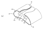
金属めっき層42は銅箔41の表面の腐食を防止するか電気がよく通じるように、そしてはんだ付けがよくできるように形成されるが、この実施例によると、図1の円の中に拡大して示したように、金属めっき層42が接触端子100の切断面に露出された銅箔41の上に形成されて銅箔41を覆う。
The
図1では、銅箔41と金属めっき層42の境界を点線で示しており、切断面で銅箔41が金属めっき層42によって覆われることを示している。
In FIG. 1, the boundary between the copper foil 41 and the
よって、従来は切断によって形成される切断面において、銅箔が外部に露出されることで塩水テストのような信頼性テストで露出された銅箔に塩水が接触し腐食を起こすため塩水テストに通ることができないか、使用中に露出された銅箔に錆が付いて信頼性が低下していた。 Therefore, conventionally, the copper foil is exposed to the outside at the cut surface formed by cutting, so that the salt water comes into contact with the copper foil exposed in the reliability test such as the salt water test and causes corrosion, so the test passes. The copper foil exposed during use was rusted and reliability was reduced.
しかし、本発明によると、切断面から露出された銅箔41を金属めっき層42で覆うことで、結果的に信頼性テストにおいて塩水の接触を根源的に遮断することができ、使用中にも銅箔41が露出されずに錆び付く恐れがないため、信頼性が向上される。
However, according to the present invention, the copper foil 41 exposed from the cut surface is covered with the
なお、リフローはんだ付けの際に切断面で銅箔41を覆うように形成された金属めっき層42の上にはんだクリームがよりよく広がって自然にはんだ付けの強度が増加するが、特に切断面におけるはんだ付けの強度が向上する。
It should be noted that the solder cream spreads better on the
特に、接触端子100の幅が長さより長ければ切断面のはんだ付けの強度は非常に重要であり、本発明はこのような場合に非常に有用である。
In particular, if the width of the
また、外部にはみ出た接着剤の上に金属めっき層42が形成されないため、電気接触端子100の外観、特に上面と下面を容易に肉眼で選別できる利点がある。
Further, since the
この実施例による電気接触端子100を製造するためには、一面に銅箔41が接着されたポリマーフィルム30で液状の接着剤層20を介在させ、コア10を連続的に包んで供給される接触端子バー(bar)を一定長さに切断するが、一例としては、接触端子バーは500mm程度の長さを有する。
In order to manufacture the
次に、接触端子バーを顧客の望む長さ、例えば3mm程度に切断して接触端子を形成し、上述したように、接触端子の銅箔41の露出面を覆うように錫や銀またはニッケル/金でめっきした金属めっき層42を形成させて、最終的な接触端子100を製造する。
Next, the contact terminal bar is cut to a length desired by the customer, for example, about 3 mm to form a contact terminal, and as described above, tin, silver, nickel / nickel / sodium is used to cover the exposed surface of the copper foil 41 of the contact terminal. A
ここで、シリコンゴム材質のコア10によって接触端子100の比重は水の比重より小さいため、バルク(bulk)方式で無電界めっきを利用して金属めっき層42を形成してもよいが、これに限らず電解めっきを適用してもよい。
Here, since the specific gravity of the
特に、無電界めっきによって金属めっき層42を形成する場合、金属めっき層42の表面粗さは増加し、その結果、はんだクリームとの接着力が向上してはんだ付けの強度が増加する。
In particular, when the
上述したように、コア10は非発泡シリコンゴムであるか発泡ゴム、例えばスポンジで構成され、接着剤層20は液状シリコンゴムが熱硬化によって形成され、ポリマーフィルム30はポリイミドフィルムで構成されて、めっき工程によって切断面に金属めっき層42が形成されない。
As described above, the
上述したように、電気接触端子100において、表面と切断面、そして幅方向の両端面を含んで外部に露出された全ての銅箔41の上には金属めっき層42が形成され、銅箔41と外部とを遮断する。
As described above, in the
次に、金属めっき層42が形成された製品をリールテーピング装置を使用してキャリアテープに自動的にリールテーピングする。
Next, the product on which the
このように、本発明の電気接触端子100は銅箔41全てを金属めっき層42で覆うことで信頼性テストで塩水の接触を根源的に遮断することができ、使用中にも錆び付く恐れがなく、リフローはんだ付けの際に切断面にもはんだクリームがよく広がってはんだ付けの強度も増加する利点がある。
As described above, the
特に、切断した後、外部に露出された銅箔41全体に対してめっき工程を行うことで、コア10の下面に位置した銅箔41の幅方向の両端面の上にも同時に金属めっき層42が形成されるため、結果的に銅箔41は外部に全く露出しない。
In particular, by performing a plating process on the entire copper foil 41 exposed to the outside after cutting, the
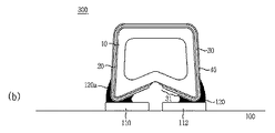
図3は、本発明の他の実施例による他の電気接触端子が回路基板にはんだ付けされた状態を示す図である。 FIG. 3 is a view illustrating a state in which another electrical contact terminal according to another embodiment of the present invention is soldered to a circuit board.
この実施例では、長さが1mmであって幅が2mmで、長さより幅が大きい電気接触端子200が開示される。
In this embodiment, an
図3の拡大された円の内部に示したように、電気接触端子200は回路基板の導電パターン110の上にはんだクリーム120を介在させてはんだ付けされるが、はんだクリーム120は銅箔41の側面に沿って広がると共に、接触端子200の切断面から銅箔41を覆う金属めっき層部分42aに沿って広がる。
As shown in the enlarged circle of FIG. 3, the
その結果、電気接触端子200の切断面から銅箔41を覆う金属めっき層部分42aに沿ってはんだクリーム120が続くため、鉛上がり性が向上されると共にはんだ付け性がよくなり、結果的にはんだ付けの強度が向上される。
As a result, since the
特に、この実施例のように、長さより幅が大きい電気接触端子200の場合、幅が大きいだけに金属めっき層部分42aが占める面積も増加するため、リフローはんだ付けの際に鉛上がり性が向上され、はんだ付け性がよくなってはんだ付けの強度が向上されることで、電気接触端子200としての信頼性及び性能が向上する。
In particular, in the case of the
図4は本発明の他の実施例による電気接触端子を示し、図5は図4の電気接触端子の下面を示し、図6は電気接触端子を回路基板に実装した状態を対比して示すが、図6aは本発明の電気接触端子であって、図6bは従来の電気接触端子である。 FIG. 4 shows an electrical contact terminal according to another embodiment of the present invention, FIG. 5 shows a lower surface of the electrical contact terminal of FIG. 4, and FIG. 6 shows a state in which the electrical contact terminal is mounted on a circuit board. 6a is an electrical contact terminal of the present invention, and FIG. 6b is a conventional electrical contact terminal.
接触端子300の下面において、金属層40が両端から一部除去されてポリマーフィルム30の両端から一定部分31が外部に露出する。
On the lower surface of the
例えば、ポリマーフィルム30の両端からそれぞれ0.05mm乃至0.3mmの幅だけ金属層40が除去されて露出するが、除去される金属層40の幅は接触端子300の幅によって異なり得る。言い換えると、除去される金属層40の幅が増加すると相対的にはんだ付けされる面積が減少し、結果的にはんだ付けの強度が弱くなる恐れがあるため、これを考慮すべきである。
For example, the
つまり、図4のCを拡大した円の内部と図5を見ると、ポリマーフィルム30の両端から幅方向に一定幅だけ、そして長さ方向に連続して金属層40が除去されてポリマーフィルム30が外部に露出する。
That is, when the inside of the circle enlarged from FIG. 4C and FIG. 5 are viewed, the
このような構成によると、接触端子300の下面に形成された金属層40の面積が減少するため、同じ構成の接触端子300に同じはんだパターンで同じ量のはんだクリームを適用する場合、接触端子300の下面の金属層40に沿って広がる溶融はんだクリームの量が減少するため、相対的に側面に沿って溶融はんだクリームが多く広がって、結果的に高い位置まではんだフィレット120aが形成されるため、はんだ付けの後で接触端子300の側面を信頼性よく支持する。その結果、側方向から接触端子300の側面を信頼性よく支持し、側方向から接触端子300に加えられる力に対して強く対応するようになる。
According to such a configuration, since the area of the
また、金属層40の両端部はポリマーフィルム30の両端部より内側に位置するため、弾性コア10の液状のポリマー接着剤を介在させてポリマーフィルム30で包んでから硬化し、接触端子300を製造する際にポリマー接着剤が完全に硬化される前にポリマーフィルム30の両端部が金属層40の弾性復元力によってコア10から剥離する傾向を大幅に減少させる。
In addition, since both ends of the
また、接触端子300の下面に折曲された金属層40が占める面積が減少し溶融されたはんだクリームが塗布される面積も減るため、はんだ付け過程で溶融はんだクリームが銅箔41を下方に引っ張る力も減って、ポリマーフィルム30の両端部がコア10から剥離して毛羽立つことを防止する。
Further, since the area occupied by the
なお、金型による外部圧力によってポリマーフィルム30に沿って流れても銅箔41の両端部によって形成された段差がはんだ付けされない接着剤の流れを阻止するため、結果的にはんだ付けの強度を上昇させ、浮く現象を減らす。
In addition, even if it flows along the
また、接触端子300の下面に折曲された金属層40が占める面積が減少することで、接触端子300の下面ではんだクリームが占める面積が減るようになり、その結果、相対的に接触端子の下面により大きい体積の空間が形成されて外部から印加される力を弾性的に受容する。
In addition, since the area occupied by the
金属層40を構成する銅箔41は、例えばポリマーフィルム30の上に銅箔41が形成された状態で露光やエッチングなどの工程によってポリマーフィルム30の一定部分31に対応する銅箔41が除去される。
The copper foil 41 constituting the
銅箔41が除去された後には、前記一実施例のように、銅箔41の上に錫や銀をめっきするか、ニッケルめっきの後、錫や金をめっきして金属めっき層42を形成する。
After the copper foil 41 is removed, the
図6aを参照すると、溶融されたはんだクリームは接触端子の下面と側面を囲む金属層40に沿って広がるが、ポリマーフィルム30の両端部と金属層40の両端部が同じであるため、溶融されたはんだクリームは主に下面に形成された金属層40に沿って広がり、相対的に側面には小さい大きさのはんだフィレット122、122aが形成される。
Referring to FIG. 6a, the melted solder cream spreads along the
よって、側方向から印加される力に十分に対応できずに接触端子が導電パターン110、112から容易に落ちる恐れがある。また、はんだ付け工程の途中、溶融されたはんだクリームによって下面の金属層40が下方に引っ張られるが、金属層40固有の復元力と溶融されたはんだクリームに引っ張られる力によってコア10に接着されたポリマーフィルム30の両端部が毛羽立って落ちるようになる。
Therefore, there is a possibility that the contact terminal may easily fall from the
一方、本発明の電気接触端子がはんだ付けされた状態を示す図5bを見ると、ポリマーフィルム30がポリマーフィルム30の両端から一定部分31が外部に露出されて接触端子300の下面に形成された金属層40の面積が小さく、相対的に同じ量の溶融はんだクリーム120は接触端子300の側面に沿って更に広がるようになり、その結果、接触端子300の側面に沿ってより高い位置まではんだフィレット120aが形成される。
Meanwhile, referring to FIG. 5 b, which shows a state in which the electrical contact terminal of the present invention is soldered, the
よって、側方向から接触端子に力が加えられても、接触端子300の側面に形成されたはんだフィレット120aがこれに十分に対応するため、接触端子300が導電パターン110、112から剥離することを減らすことができる。
Therefore, even if a force is applied to the contact terminal from the side direction, the
また、はんだ付けの際に溶融されたはんだクリームによって下面の金属層40が下方に引っ張られるが、金属層40の両端部がポリマーフィルム30の両端部より内側に位置するため溶融されたはんだクリームによって引っ張られる力が減少するだけでなく、金属層40の面積が減少して固有の弾性復元力が減少し、その結果コア10に接着されたポリマーフィルム30の両端部が金属層40によって下方に引っ張られて落ちる現象を防止することができる。
In addition, the
一方、接着剤が塗布されたポリマーフィルム30でコア10を包み、金型(図示せず)を通過しながら圧着及び熱硬化によってポリマーフィルム30がコア10に接着される際、金型による外部圧力によってポリマーフィルム30の両端からはみ出る接着剤がポリマーフィルム30に沿って流れたとしても、金属層40の両端部が段差を成すため接着剤の流れを阻止することができる。このような接着剤ははんだクリームによるはんだ付けができないため、このような段差は結果的に接着端子のはんだ付けの強度をよくし、浮く現象を減少させる。
On the other hand, when the
前記実施例では、電気接触端子100、200、300が回路基板の導電パターンにはんだクリームによってはんだ付けされて対向する電気伝導性対象物と接触する場合を例に挙げて説明したが、これに限ることなく、上述したように回路基板の導電パターンと電気伝導性対象物との間に強制的に挟まれて設置されてもよい。この場合、リフローはんだ付けのような工程がないため、構成要素の材質が耐熱性を有する必要はない。
In the above-described embodiment, the case where the
これまで本発明の実施例を中心に説明したが、当業者の水準で多様な変更や変形が加えられてもよい。このような変更と変形が本発明の範囲を逸脱しない限り、本発明に属するといえる。本発明の権利範囲は、以下に記載される特許請求の範囲によって判断されるべきである。
Although the embodiments of the present invention have been described so far, various changes and modifications may be made at the level of those skilled in the art. Unless such changes and modifications depart from the scope of the present invention, it can be said to belong to the present invention. The scope of the present invention should be determined by the claims set forth below.
Claims (22)
前記銅箔の外部に露出される全ての面に金属めっき層が形成され
前記露出面は、前記銅箔の表面と幅方向の両端面及び前記電気接触端子を切断して形成される前記銅箔の切断面を含む、ことを特徴とする弾性電気接触端子。 An elastic core, a polymer film is adhered while wrapping the core with interposition of the adhesive layer, and the soldering which can copper foil to be bonded while wrapping the polymer film, in the including elastic electric contact terminal,
A metal plating layer is formed on all surfaces exposed to the outside of the copper foil.
The elastic electric contact terminal , wherein the exposed surface includes a surface of the copper foil, both end surfaces in the width direction, and a cut surface of the copper foil formed by cutting the electric contact terminal.
前記金属層は前記ポリマーフィルムの上に金属シードをスパッタリングした後、その上にめっきによって形成される銅めっき層を含み、前記銅めっき層の表面、幅方向の両端面及び電気接触端子を切断して形成される前記銅めっき層の切断面を覆うように金属めっき層が形成されることを特徴とする弾性電気接触端子。 An elastic core, a polymer film that is bonded while wrapping the core through an adhesive layer, and a solderable metal layer that is bonded while wrapping the polymer film,
After the metal layer is obtained by sputtering a metal seed on the polymer film comprises a copper plating layer formed by plating thereon, the surface of the copper plating layer, the end surfaces and the electrical contact terminal in the width direction cutting An elastic electrical contact terminal, wherein a metal plating layer is formed so as to cover a cut surface of the copper plating layer formed.
前記シリコンゴムの長さ方向に液状のシリコンゴム接着剤を連続して塗布するステップと、
一面に銅箔が接着されたポリマーフィルムの他面が前記液状のシリコンゴム接着剤を介在して前記シリコンゴムを包んだ後、前記シリコンゴム接着剤を硬化して前記シリコンゴムと前記ポリマーフィルムを接着して積層体を形成するステップと、
前記積層体を一定長さに切断するステップと、
前記銅箔の表面、幅方向の両端面及び前記切断によって形成された前記銅箔の切断面に金属をめっきして金属めっき層を形成するステップと、を含むことを特徴とする弾性電気接触端子の製造方法。 Comprising the steps of: providing a silicone rubber formed by roll,
Continuously applying a liquid silicone rubber adhesive in the length direction of the silicone rubber;
The other side of the polymer film having a copper foil bonded on one side wraps the silicone rubber with the liquid silicone rubber adhesive interposed therebetween, and then the silicone rubber adhesive is cured to form the silicone rubber and the polymer film. Bonding to form a laminate;
Cutting the laminate to a certain length;
Forming a metal plating layer by plating a metal on the surface of the copper foil, both end surfaces in the width direction, and the cut surface of the copper foil formed by the cutting. Manufacturing method.
The method of manufacturing an elastic electrical contact terminal according to claim 21 , wherein the metal plating layer is formed by electroless plating, and the strength of soldering is improved by increasing the surface roughness.
Applications Claiming Priority (5)
| Application Number | Priority Date | Filing Date | Title |
|---|---|---|---|
| KR20150040000 | 2015-03-23 | ||
| KR10-2015-0040000 | 2015-03-23 | ||
| KR1020150075063A KR101711016B1 (en) | 2015-03-23 | 2015-05-28 | Elastic electric contact terminal having improved environmental property and Method for making the same |
| KR10-2015-0075063 | 2015-05-28 | ||
| PCT/KR2015/006956 WO2016153116A1 (en) | 2015-03-23 | 2015-07-06 | Elastic electric contact terminal with improved environmental resistance, and fabrication method therefor |
Publications (2)
| Publication Number | Publication Date |
|---|---|
| JP2017532741A JP2017532741A (en) | 2017-11-02 |
| JP6400845B2 true JP6400845B2 (en) | 2018-10-03 |
Family
ID=57165246
Family Applications (1)
| Application Number | Title | Priority Date | Filing Date |
|---|---|---|---|
| JP2017516940A Active JP6400845B2 (en) | 2015-03-23 | 2015-07-06 | Elastic electrical contact terminal with improved environmental resistance and method for manufacturing the same |
Country Status (4)
| Country | Link |
|---|---|
| US (1) | US10128584B2 (en) |
| EP (1) | EP3276751B1 (en) |
| JP (1) | JP6400845B2 (en) |
| KR (1) | KR101711016B1 (en) |
Families Citing this family (9)
| Publication number | Priority date | Publication date | Assignee | Title |
|---|---|---|---|---|
| CN110391527A (en) * | 2018-04-23 | 2019-10-29 | 卓英社有限公司 | Electric contact terminal and its mounting structure, installation method and mounting device |
| KR102173791B1 (en) * | 2018-12-27 | 2020-11-04 | 김만곤 | Silicone Gap Supporter |
| US11929212B2 (en) * | 2019-04-23 | 2024-03-12 | Intel Corporation | Method to form high capacitance thin film capacitors (TFCs) as embedded passives in organic substrate packages |
| KR102236798B1 (en) * | 2019-05-21 | 2021-04-06 | 조인셋 주식회사 | Elastic electric connect terminal assembly |
| KR102416027B1 (en) * | 2019-11-15 | 2022-07-05 | 조인셋 주식회사 | Elastic electrical contact terminal |
| KR102258846B1 (en) * | 2020-01-15 | 2021-06-01 | 조인셋 주식회사 | Press-contact electrical interconnector |
| CN112351666A (en) * | 2020-07-27 | 2021-02-09 | 深圳市卓汉材料技术有限公司 | Wrapped heat-conducting grounding elastic piece and electronic equipment |
| CN112310671B (en) * | 2020-07-27 | 2022-04-12 | 深圳市卓汉材料技术有限公司 | High-temperature-resistant grounding elastic piece and electronic equipment |
| CN113993362B (en) | 2021-09-30 | 2022-05-10 | 深圳市卓汉材料技术有限公司 | Grounding elastic body and electronic equipment |
Family Cites Families (17)
| Publication number | Priority date | Publication date | Assignee | Title |
|---|---|---|---|---|
| US4857668A (en) * | 1988-04-15 | 1989-08-15 | Schlegel Corporation | Multi-function gasket |
| KR200182453Y1 (en) * | 1999-11-22 | 2000-05-15 | 익스팬전자주식회사 | Conductive gasket for improving contact reliablity |
| JP2003197289A (en) * | 2001-12-25 | 2003-07-11 | Shin Etsu Polymer Co Ltd | Pressure-contact electric connector |
| WO2005053328A1 (en) * | 2003-11-28 | 2005-06-09 | Joinset Co., Ltd. | Electric conductive gasket |
| KR200390440Y1 (en) | 2005-04-14 | 2005-07-22 | 조인셋 주식회사 | Zebra typed anisotropic conductive connector terminal |
| JP4427565B2 (en) * | 2006-07-03 | 2010-03-10 | 日本ジッパーチュービング株式会社 | Solderable elastic electrical contact terminals |
| KR200428000Y1 (en) * | 2006-07-03 | 2006-10-04 | 조인셋 주식회사 | Solderable Electric contact terminal |
| KR100783588B1 (en) | 2006-11-08 | 2007-12-07 | 조인셋 주식회사 | Solderable electric contact terminal |
| JP4739169B2 (en) * | 2006-11-13 | 2011-08-03 | 北川工業株式会社 | Elastic contact |
| MY147054A (en) * | 2008-03-07 | 2012-10-15 | Joinset Co Ltd | Solderable elastic electric contact terminal |
| KR101001354B1 (en) | 2008-07-01 | 2010-12-14 | 조인셋 주식회사 | Reflow solderable electric contacts having elasticity |
| KR101018735B1 (en) * | 2008-12-15 | 2011-03-04 | 조인셋 주식회사 | Solderable Elastic Conductive Contact Terminal |
| JP2011086557A (en) * | 2009-10-16 | 2011-04-28 | Zippertubing (Japan) Ltd | Jumper for surface mounting |
| KR100993253B1 (en) * | 2010-04-28 | 2010-11-10 | 김선기 | Elastic electric contact terminal |
| KR101201410B1 (en) | 2011-05-31 | 2012-11-14 | 주식회사 이엔씨테크 | Elastic electric contact terminal for the printed circuit board |
| KR101084282B1 (en) * | 2011-06-15 | 2011-11-17 | 김선기 | Solderable elastic electric contact terminal |
| KR101562938B1 (en) * | 2013-08-13 | 2015-10-30 | 조인셋 주식회사 | Electric contact terminal |
-
2015
- 2015-05-28 KR KR1020150075063A patent/KR101711016B1/en active IP Right Grant
- 2015-07-06 JP JP2017516940A patent/JP6400845B2/en active Active
- 2015-07-06 EP EP15886564.2A patent/EP3276751B1/en active Active
-
2017
- 2017-03-20 US US15/463,509 patent/US10128584B2/en active Active
Also Published As
| Publication number | Publication date |
|---|---|
| KR101711016B1 (en) | 2017-02-28 |
| US10128584B2 (en) | 2018-11-13 |
| KR20160113956A (en) | 2016-10-04 |
| EP3276751B1 (en) | 2021-01-06 |
| US20170229795A1 (en) | 2017-08-10 |
| EP3276751A4 (en) | 2018-11-21 |
| JP2017532741A (en) | 2017-11-02 |
| EP3276751A1 (en) | 2018-01-31 |
Similar Documents
| Publication | Publication Date | Title |
|---|---|---|
| JP6400845B2 (en) | Elastic electrical contact terminal with improved environmental resistance and method for manufacturing the same | |
| CN102237582B (en) | Elastic electric contact terminal | |
| KR101662261B1 (en) | Solderable elastic electric contact terminal | |
| KR101001354B1 (en) | Reflow solderable electric contacts having elasticity | |
| KR100892720B1 (en) | Solderable elastic electric contact terminal | |
| KR101084282B1 (en) | Solderable elastic electric contact terminal | |
| CN105990728B (en) | Elastic electric contact terminal with improved environmental resistance and method for manufacturing the same | |
| KR101022037B1 (en) | Electric and Elastic Contact Terminal | |
| US20160336093A1 (en) | Elastic electric contact terminal adapted to small size | |
| JP6121583B2 (en) | Elastic electrical contact terminal | |
| KR101025792B1 (en) | Solderable electric and elastic contacts | |
| KR200442294Y1 (en) | Solderable Electric contact terminal | |
| CN107809012B (en) | It is suitable for the centreless elastic electric contact terminal of low clearance | |
| KR101018735B1 (en) | Solderable Elastic Conductive Contact Terminal | |
| KR101046765B1 (en) | Solderable Elastic Electrical Contact Terminals | |
| KR101735656B1 (en) | Elastic electric contact terminal having improved environmental property and Method for making the same | |
| KR101038980B1 (en) | Electric contacts for SMT | |
| KR101001355B1 (en) | Elastic conductive Contact Terminal for Surface Mount | |
| KR101793719B1 (en) | Elastic electric contact terminal having improved corrosive property and Method for making the same | |
| KR101804882B1 (en) | Solderable Elastic Electric Contact Terminal | |
| KR101759712B1 (en) | Elastic electric contact terminal having stability for signal transfer | |
| KR20180028392A (en) | Coreless elastic electric contact terminal | |
| KR20150024242A (en) | Solderable Intenna and Method for making the same |
Legal Events
| Date | Code | Title | Description |
|---|---|---|---|
| A977 | Report on retrieval |
Free format text: JAPANESE INTERMEDIATE CODE: A971007 Effective date: 20180216 |
|
| A131 | Notification of reasons for refusal |
Free format text: JAPANESE INTERMEDIATE CODE: A131 Effective date: 20180227 |
|
| A521 | Request for written amendment filed |
Free format text: JAPANESE INTERMEDIATE CODE: A523 Effective date: 20180516 |
|
| TRDD | Decision of grant or rejection written | ||
| A01 | Written decision to grant a patent or to grant a registration (utility model) |
Free format text: JAPANESE INTERMEDIATE CODE: A01 Effective date: 20180821 |
|
| A61 | First payment of annual fees (during grant procedure) |
Free format text: JAPANESE INTERMEDIATE CODE: A61 Effective date: 20180905 |
|
| R150 | Certificate of patent or registration of utility model |
Ref document number: 6400845 Country of ref document: JP Free format text: JAPANESE INTERMEDIATE CODE: R150 |
|
| R250 | Receipt of annual fees |
Free format text: JAPANESE INTERMEDIATE CODE: R250 |
|
| R250 | Receipt of annual fees |
Free format text: JAPANESE INTERMEDIATE CODE: R250 |
|
| R250 | Receipt of annual fees |
Free format text: JAPANESE INTERMEDIATE CODE: R250 |