JP6361290B2 - Image processing apparatus, display apparatus, and image processing method - Google Patents
Image processing apparatus, display apparatus, and image processing method Download PDFInfo
- Publication number
- JP6361290B2 JP6361290B2 JP2014112522A JP2014112522A JP6361290B2 JP 6361290 B2 JP6361290 B2 JP 6361290B2 JP 2014112522 A JP2014112522 A JP 2014112522A JP 2014112522 A JP2014112522 A JP 2014112522A JP 6361290 B2 JP6361290 B2 JP 6361290B2
- Authority
- JP
- Japan
- Prior art keywords
- data
- storage unit
- pixels
- unit
- stored
- Prior art date
- Legal status (The legal status is an assumption and is not a legal conclusion. Google has not performed a legal analysis and makes no representation as to the accuracy of the status listed.)
- Expired - Fee Related
Links
- 238000012545 processing Methods 0.000 title claims description 45
- 238000003672 processing method Methods 0.000 title claims description 6
- 238000012937 correction Methods 0.000 claims description 89
- 239000013598 vector Substances 0.000 claims description 56
- 238000000034 method Methods 0.000 claims description 22
- 238000010586 diagram Methods 0.000 description 20
- 230000003287 optical effect Effects 0.000 description 19
- 238000012986 modification Methods 0.000 description 14
- 230000004048 modification Effects 0.000 description 14
- 239000000872 buffer Substances 0.000 description 12
- 239000000284 extract Substances 0.000 description 7
- 230000006870 function Effects 0.000 description 4
- 230000000694 effects Effects 0.000 description 2
- 230000005484 gravity Effects 0.000 description 2
- 239000007787 solid Substances 0.000 description 2
- 241000406668 Loxodonta cyclotis Species 0.000 description 1
- 230000005540 biological transmission Effects 0.000 description 1
- 230000003111 delayed effect Effects 0.000 description 1
- 229910052736 halogen Inorganic materials 0.000 description 1
- 150000002367 halogens Chemical class 0.000 description 1
- 238000003384 imaging method Methods 0.000 description 1
- 239000004973 liquid crystal related substance Substances 0.000 description 1
- 239000011159 matrix material Substances 0.000 description 1
- 238000005259 measurement Methods 0.000 description 1
- QSHDDOUJBYECFT-UHFFFAOYSA-N mercury Chemical compound [Hg] QSHDDOUJBYECFT-UHFFFAOYSA-N 0.000 description 1
- 229910052753 mercury Inorganic materials 0.000 description 1
- 229910001507 metal halide Inorganic materials 0.000 description 1
- 150000005309 metal halides Chemical class 0.000 description 1
- 239000004065 semiconductor Substances 0.000 description 1
- 238000004904 shortening Methods 0.000 description 1
- 230000001360 synchronised effect Effects 0.000 description 1
- 238000012360 testing method Methods 0.000 description 1
Images


Classifications
-
- G—PHYSICS
- G06—COMPUTING; CALCULATING OR COUNTING
- G06T—IMAGE DATA PROCESSING OR GENERATION, IN GENERAL
- G06T3/00—Geometric image transformation in the plane of the image
-
- G—PHYSICS
- G06—COMPUTING; CALCULATING OR COUNTING
- G06T—IMAGE DATA PROCESSING OR GENERATION, IN GENERAL
- G06T1/00—General purpose image data processing
- G06T1/60—Memory management
-
- G06T3/18—
Description
本発明は、画像を補正する技術に関する。 The present invention relates to a technique for correcting an image.
プロジェクターにおいては、スクリーンと投写系との位置関係が理想的な状態からずれると、スクリーンに投写される画像が歪む。この歪みを解消するため、入力映像に対してこれと逆の歪みを与える画像処理が用いられている。この画像処理は入力映像のうち処理対象の画素に対して、この画素に対応するオフセットベクトルで指定される位置にある他の画素のデータを参照して行われる。この場合において、オフセットベクトルの成分が整数でないときは、オフセットベクトルで指定される位置の周囲の4画素のデータを参照して、画像処理が行われる。 In the projector, when the positional relationship between the screen and the projection system deviates from an ideal state, the image projected on the screen is distorted. In order to eliminate this distortion, image processing that gives a distortion opposite to the input video is used. This image processing is performed on the pixel to be processed in the input video with reference to data of other pixels at the position specified by the offset vector corresponding to this pixel. In this case, when the component of the offset vector is not an integer, image processing is performed with reference to the data of the four pixels around the position specified by the offset vector.
4画素のデータを用いて画像処理を行うには、当然のことながら4画素分のデータをメモリーから読み出す必要がある。すなわち、1つのRAMに4回アクセスする必要があり、データの読み出しに4クロック分の時間がかかってしまう。例えば、オフセットベクトルの成分が整数である場合と比較すると、データの読み出しに4倍の時間がかかってしまい、その分、映像信号出力が遅くなってしまう。 In order to perform image processing using data of 4 pixels, it is natural that data for 4 pixels needs to be read from the memory. That is, it is necessary to access one RAM four times, and it takes time for four clocks to read data. For example, compared with the case where the offset vector component is an integer, it takes four times longer to read data, and the video signal output is delayed correspondingly.
特許文献1は、垂直方向の2画素のデータを用いてズーム画像を生成するため、画像クロックの2倍のクロックレートでメモリーにアクセスする技術を開示している。
特許文献1に記載の技術においては、高速のクロックを生成する必要があり、画像処理回路が高コストになってしまうという問題があった。
In the technique described in
これに対し本発明は、メモリーアクセス用の高速クロックを用いずに、補正に用いられるデータを得る時間を短縮する技術を提供する。 In contrast, the present invention provides a technique for shortening the time for obtaining data used for correction without using a high-speed clock for memory access.
本発明は、r行c列の画素を有する表示部に表示される画像を処理する画像処理装置であって、前記画像のうちk1行分のデータに相当する複数の記憶領域を有し、当該複数の記憶領域の各々に、隣り合う少なくとも2画素のデータを記憶する第1記憶部と、前記画像のうちk2行分(k1およびk2は、Omax<(k1+k2)<rを満たす自然数であり、Omaxは前記表示部に対してあらかじめ設定されたオフセット最大値である)のデータに相当する複数の記憶領域を有し、当該複数の記憶領域の各々に、前記第1記憶部にデータが記憶されている画素とは異なる行において隣り合う少なくとも2画素のデータを記憶する第2記憶部と、前記r行c列の画素のうち処理対象となる対象画素のデータを、前記第1記憶部および前記第2記憶部において当該対象画素に対応するオフセットベクトルにより示される位置に対応する記憶領域に記憶されている複数の画素のデータを用いて補正を行う補正部とを有する画像処理装置を提供する。 The present invention is an image processing apparatus for processing an image displayed on a display unit having pixels of r rows and c columns, and having a plurality of storage areas corresponding to data for k1 rows of the image, A first storage unit that stores data of at least two adjacent pixels in each of a plurality of storage areas, and k2 rows of the image (k1 and k2 are natural numbers that satisfy Omax <(k1 + k2) <r; Omax is a maximum offset value set in advance for the display unit), and each of the plurality of storage regions stores data in the first storage unit. A second storage unit that stores data of at least two pixels adjacent to each other in a row that is different from the current pixel, and data of a target pixel to be processed among the pixels in the r row and the c column, the first storage unit and the First In the storage unit using the data of a plurality of pixels stored in the storage area corresponding to the position indicated by the offset vector corresponding to the target pixel to provide an image processing apparatus and a correcting unit for correcting.
この画像処理装置によれば、メモリーアクセス用の高速クロックを用いずに、補正に用いられるデータを得る時間を短縮することができる。 According to this image processing apparatus, the time for obtaining data used for correction can be shortened without using a high-speed clock for memory access.
前記オフセットベクトルにより示される位置が前記第1記憶部の第1記憶領域に記憶されている画素および前記第2記憶部の第2記憶領域に記憶されている画素の間の位置だった場合、前記補正部は、当該第1記憶領域および当該第2記憶領域に記憶されているデータを用いて、前記補正を行ってもよい。 When the position indicated by the offset vector is a position between a pixel stored in the first storage area of the first storage unit and a pixel stored in the second storage area of the second storage unit, The correction unit may perform the correction using data stored in the first storage area and the second storage area.
この画像処理装置によれば、オフセットベクトルにより示される位置が第1記憶部の第1記憶領域に記憶されている画素および第2記憶部の第2記憶領域に記憶されている画素の間の位置であった場合も補正をすることができる。 According to this image processing apparatus, the position indicated by the offset vector is a position between the pixel stored in the first storage area of the first storage unit and the pixel stored in the second storage area of the second storage unit. If it is, it can be corrected.
前記オフセットベクトルにより示される位置が前記第1記憶部の2つの記憶領域に記憶されている2つの画素の間に対応する位置だった場合、前記補正部は、当該2つの記憶領域から順次読み出されたデータを用いて、前記補正を行ってもよい。 When the position indicated by the offset vector corresponds to a position between two pixels stored in the two storage areas of the first storage unit, the correction unit sequentially reads from the two storage areas. The correction may be performed using the corrected data.
この画像処理装置によれば、オフセットベクトルにより示される位置が第1記憶部の2つの記憶領域に記憶されている2つの画素の間に対応する位置であった場合も補正をすることができる。 According to this image processing apparatus, it is possible to perform correction even when the position indicated by the offset vector is a position corresponding to between two pixels stored in the two storage areas of the first storage unit.
この画像処理装置は、直近の単位期間において前記補正部が用いたデータを記憶するキャッシュ記憶部を有し、前記対象画素が、前記直近の単位期間から1画素分移動した場合、前記補正部は、前記キャッシュ記憶部に記憶されているデータ、並びに前記第1記憶部および前記第2記憶部のいずれかに記憶されているデータを用いて前記補正を行ってもよい。 The image processing apparatus includes a cache storage unit that stores data used by the correction unit in the most recent unit period. When the target pixel moves by one pixel from the most recent unit period, the correction unit The correction may be performed using data stored in the cache storage unit and data stored in either the first storage unit or the second storage unit.
この画像処理装置によれば、キャッシュ記憶部を用いない場合と比較してよりデータ読み出しの時間を短縮することができる。 According to this image processing apparatus, it is possible to shorten the data reading time as compared with the case where the cache storage unit is not used.
この画像処理装置は、前記第1記憶部にデータが記憶されている画素と同じ行において当該画素と隣り合う画素を含み、互いに隣り合う少なくとも2画素のデータを記憶する第3記憶部と、前記第2記憶部にデータが記憶されている画素と同じ行において当該画素と隣り合う画素を含み、互いに隣り合う少なくとも2画素のデータを記憶する第4記憶部とを有し、前記補正部は、前記対象画素のデータを、前記第1記憶部、前記第2記憶部、前記第3記憶部、および前記第4記憶部において当該対象画素に対応するオフセットベクトルにより示される位置に対応する記憶領域に記憶されている複数の画素のデータを用いて補正を行ってもよい。 The image processing apparatus includes a third storage unit that includes pixels adjacent to the pixel in the same row as the pixels in which data is stored in the first storage unit, and stores data of at least two pixels adjacent to each other; A fourth storage unit that stores data of at least two pixels adjacent to each other and includes a pixel adjacent to the pixel in the same row as the pixel in which data is stored in the second storage unit, and the correction unit includes: Data of the target pixel is stored in a storage area corresponding to a position indicated by an offset vector corresponding to the target pixel in the first storage unit, the second storage unit, the third storage unit, and the fourth storage unit. You may correct | amend using the data of the some pixel memorize | stored.
この画像処理装置によれば、第3記憶部および第4記憶部を用いない場合と比較してよりデータ読み出しの時間を短縮することができる。 According to this image processing apparatus, it is possible to shorten the data reading time as compared with the case where the third storage unit and the fourth storage unit are not used.
また、本発明は、r行c列の画素を有する表示部と、前記表示部に表示される画像のうちk1行分のデータに相当する複数の記憶領域を有し、当該複数の記憶領域の各々に、隣り合う少なくとも2画素のデータを記憶する第1記憶部と、前記画像のうちk2行分(k1およびk2は、Omax<(k1+k2)<rを満たす自然数であり、Omaxは前記表示部に対してあらかじめ設定されたオフセット最大値である)のデータに相当する複数の記憶領域を有し、当該複数の記憶領域の各々に、前記第1記憶部にデータが記憶されている画素とは異なる行において隣り合う少なくとも2画素のデータを記憶する第2記憶部と、前記r行c列の画素のうち処理対象となる対象画素のデータを、前記第1記憶部および前記第2記憶部において当該対象画素に対応するオフセットベクトルにより示される位置に対応する記憶領域に記憶されている複数の画素のデータを用いて補正を行う補正部とを有する表示装置を提供する。 In addition, the present invention includes a display unit having pixels of r rows and c columns, and a plurality of storage areas corresponding to data for k1 rows in the image displayed on the display unit. A first storage unit that stores data of at least two pixels adjacent to each other, and k2 rows of the image (k1 and k2 are natural numbers satisfying Omax <(k1 + k2) <r, and Omax is the display unit A pixel having a plurality of storage areas corresponding to the data of the offset maximum value set in advance for each of the plurality of storage areas and the data being stored in the first storage unit A second storage unit that stores data of at least two pixels adjacent to each other in different rows, and data of a target pixel to be processed among pixels in the r rows and c columns are stored in the first storage unit and the second storage unit. Concerned To provide a display device having a correcting unit that performs correction using the data of a plurality of pixels stored in the corresponding storage area in the position indicated by the offset vector corresponding to the elephant pixel.
この表示装置によれば、メモリーアクセス用の高速クロックを用いずに、補正に用いられるデータを得る時間を短縮することができる。 According to this display device, the time for obtaining data used for correction can be shortened without using a high-speed clock for memory access.
さらに、本発明は、r行c列の画素を有する表示部に表示される画像を処理する画像処理方法であって、前記画像のうちk1行分のデータに相当する複数の記憶領域を有し、当該複数の記憶領域の各々に、隣り合う少なくとも2画素のデータを第1記憶部に記憶するステップと、前記画像のうちk2行分(k1およびk2は、Omax<(k1+k2)<rを満たす自然数であり、Omaxは前記表示部に対してあらかじめ設定されたオフセット最大値である)のデータに相当する複数の記憶領域を有し、当該複数の記憶領域の各々に、前記第1記憶部にデータが記憶されている画素とは異なる行において隣り合う少なくとも2画素のデータを第2記憶部に記憶するステップと、前記r行c列の画素のうち処理対象となる対象画素のデータを、前記第1記憶部および前記第2記憶部において当該対象画素に対応するオフセットベクトルにより示される位置に対応する記憶領域に記憶されている複数の画素のデータを用いて補正を行うステップとを有する画像処理方法を提供する。 Furthermore, the present invention is an image processing method for processing an image displayed on a display unit having pixels of r rows and c columns, and having a plurality of storage areas corresponding to data for k1 rows of the image. Storing the data of at least two adjacent pixels in each of the plurality of storage areas in the first storage unit, and k2 rows of the image (k1 and k2 satisfy Omax <(k1 + k2) <r) A natural number, and Omax is a preset offset maximum value for the display unit), and each of the plurality of storage regions has the first storage unit. Storing data of at least two pixels adjacent to each other in a row different from the pixel in which the data is stored in the second storage unit; and data of a target pixel to be processed among the pixels in the r row and the c column An image having a step of performing correction using data of a plurality of pixels stored in a storage area corresponding to a position indicated by an offset vector corresponding to the target pixel in the first storage unit and the second storage unit. A processing method is provided.
この画像処理方法によれば、メモリーアクセス用の高速クロックを用いずに、補正に用いられるデータを得る時間を短縮することができる。 According to this image processing method, the time for obtaining data used for correction can be shortened without using a high-speed clock for memory access.
1.構成
図1は、一実施形態に係る表示装置1の構成を示すブロック図である。表示装置1は、例えば、自動車、電車、または飛行機のフロントガラスに画像を投写する投写型の表示装置、いわゆるHUD(Head-Up Display)である。表示装置1が自動車に用いられる場合、投写される画像は、例えば、カーナビゲーションの画面または各種計器(例えば速度計や回転計)の測定結果を示す画像である。
1. Configuration FIG. 1 is a block diagram illustrating a configuration of a
表示装置1は、ホスト装置11と、コントローラー12と、投写ユニット13と、記憶部14と、IF部15と、操作パネル16とを有する。
The
ホスト装置11は、表示装置1の他の構成要素を制御する。ホスト装置11は、CPU(Central Processing Unit)111と、ROM(Read Only Memory)112と、RAM(Random Access Memory)113とを有する。CPU111は、表示装置1の各部を制御する制御装置である。ROM112は、各種プログラムおよびデータを記憶した不揮発性の記憶装置である。RAM113は、データを記憶する揮発性の記憶装置であり、CPU111が処理を実行する際のワークエリアとして機能する。
The
コントローラー12は、投写ユニット13を制御する装置である。この例で、コントローラー12は、入力された映像信号(以下「入力映像信号」という)に所定の画像処理を施す画像処理装置として機能する。コントローラー12は、画像処理を施した映像信号を、投写ユニット13に出力する。
The
投写ユニット13は、画像処理が施された映像信号に従って、スクリーンに画像を投写する。投写ユニット13は、光源、光変調器131、および光学系、並びにこれらの駆動回路を有する(光変調器131以外は図示略)。光源は、高圧水銀ランプ、ハロゲンランプ、若しくはメタルハライドランプなどのランプ、またはLED(Light Emitting Diode)若しくはレーザーダイオードなどの固体光源である。光変調器131は、光源から照射された光を映像信号に応じて変調する装置であり、例えば液晶パネルまたはDMD(Digital Mirror Device)等の表示部を有する。光変調器131は、r行c列のマトリクス状に配置された画素を有し、画素毎に光を変調する。光学系は、光変調器により変調された光をスクリーンに投写する素子であり、例えばレンズおよびプリズムを有する。
The
記憶部14は、データおよびプログラムを記憶する不揮発性の記憶装置、例えばHDD(Hard Disk Drive)またはSSD(Solid State Drive)である。記憶部14は、例えば、カーナビゲーションを実行するためのプログラムおよび地図データを記憶している。ホスト装置11は、記憶部14に記憶されているプログラムおよびデータを用いてカーナビゲーションの画像を生成し、後段の回路に出力する。
The
IF部15は、外部装置(例えば各種計器)と信号またはデータの送受信を仲介するインターフェースである。IF部15は、外部装置と信号またはデータの送受信をするための端子を有する。
The
操作パネル16は、ユーザーが表示装置1に対し指示を入力するための入力装置であり、例えば、キーパッド、ボタン、またはタッチパネルを含む。
The operation panel 16 is an input device for a user to input an instruction to the
図2は、コントローラー12の構成を示す図である。コントローラー12は、VRAM(Video RAM)121と、アービター122と、映像入力部123と、書き込みIF124と、読み出しアドレス生成部125と、読み出しIF126と、補正部127と、映像出力部128と、オフセットテーブル129とを有する。
FIG. 2 is a diagram illustrating the configuration of the
VRAM121は、全部でk行分の画像データを記憶する記憶領域を有し、フレームバッファーとして用いられるメモリー(記憶部)である。ここで、kは、
Omax<k<r …(1)
を満たす自然数である。Omaxは、用いられる光変調器131に応じてあらかじめ設定されたオフセット最大値である。オフセット最大値については後述する。
The
Omax <k <r (1)
It is a natural number that satisfies Omax is a maximum offset value set in advance according to the
VRAM121は、詳細には、VRAM1211、VRAM1212、VRAM1213、およびVRAM1214の4つのフレームバッファー(第1〜第4記憶部の一例)を有する。VRAM1211、VRAM1212、VRAM1213、およびVRAM1214を区別する必要が無いときは、VRAM121と記載する。VRAM1211、VRAM1212、VRAM1213、およびVRAM1214は、それぞれ、k1、k2、k3、およびk4行分のデータを記憶する記憶領域を有する。なお、k1、k2、k3、およびk4は、k1+k2+k3+k4=kを満たす自然数である。また、k1=k2=k3=k4であることが好ましい。
Specifically, the
VRAM1211〜1214の各々は、複数の単位記憶領域に区分されている。各単位記憶領域は、アドレスにより特定される。各単位記憶領域には、行方向において隣り合う(一連の)少なくとも2つの画素のデータが記憶される。すなわち、あるアドレスで特定される記憶領域には、行方向において隣り合う一連の少なくとも2画素のデータがパッキングされて記憶されており、データの読み出しおよび書き込みはこれら複数の画素を単位として行われる。 Each of the VRAMs 1211 to 1214 is divided into a plurality of unit storage areas. Each unit storage area is specified by an address. Each unit storage area stores data of at least two (sequential) pixels adjacent in the row direction. That is, in a storage area specified by a certain address, data of a series of at least two pixels adjacent in the row direction are packed and stored, and reading and writing of data are performed in units of the plurality of pixels.
本実施形態において、各単位記憶領域には、隣り合う2つの画素のデータが記憶されている。例えば、1画素のデータが24ビットである場合には、単位記憶領域は48ビットの記憶容量を有する。上位24ビットにはx座標が小さい画素のデータが、下位24ビットにはx座標が大きい画素のデータが記憶されている。なお、VRAM1211〜1214の記憶領域と画素との関係については後述する。 In the present embodiment, data of two adjacent pixels is stored in each unit storage area. For example, when the data of one pixel is 24 bits, the unit storage area has a storage capacity of 48 bits. The upper 24 bits store pixel data with a small x coordinate, and the lower 24 bits store pixel data with a large x coordinate. The relationship between the storage areas of the VRAMs 1211 to 1214 and the pixels will be described later.
なおVRAM121は、必ずしも全体でk行c列の記憶領域を有していなくてもよい。VRAM121はk行c列よりもより多くの記憶領域を有していてもよい。この場合、VRAM121の一部の記憶領域をブロック分割して用いることができる。あるいは、ハードウェアとしては単一のRAMの記憶領域を4つに分割して、それぞれVRAM1211〜1214として用いてもよい。また、図2ではコントローラー12がVRAM121を内蔵している例を示したが、VRAM121はコントローラー12の外部に設けられていてもよい。
Note that the
アービター122は、VRAM121へアクセスする権利を調停する回路である。
The
映像入力部123は、ホスト装置11から映像信号(「入力映像信号」という)を受け付ける。映像入力部123は、入力映像信号を、書き込みIF124に出力する。
The
書き込みIF124は、入力映像信号をデータとしてVRAM121に書き込む。このとき、書き込みIF124は、VRAM121の記憶領域のうち、ライトカウンターで指定される行に対応する記憶領域にデータを書き込む。ライトカウンターは、データの書き込みが行われる行を指定するパラメーターである。書き込みIF124は、ライトカウンターを記憶するためのレジスター(記憶部)を有している(図示略)。
The write IF 124 writes the input video signal as data in the
読み出しアドレス生成部125は、処理対象画素のデータの補正に用いられるデータが記憶されている記憶領域を示すアドレス(以下「読み出しアドレス」という)を生成する。読み出しアドレス生成部125は、リードカウンターおよびオフセットベクトルを用いて読み出しアドレスを生成する。リードカウンターは、データ読み出しの基準となる行を指定するパラメーターである。読み出しアドレス生成部125は、リードカウンターを記憶するためのレジスター(記憶部)を有している(図示略)。オフセットベクトルは、オフセットテーブル129から得られる。オフセットテーブル129は、オフセットベクトルが記録されたテーブルを記憶したメモリーである。オフセットベクトルについては後述する。
The read
読み出しIF126は、VRAM121からデータを読み出す。この例で、1つのアドレスで指定される記憶領域には、隣り合う2つの画素のデータが含まれている。読み出しIF126は、読み出したデータのうち、画像処理に用いるデータを、補正部124に出力する。
The read IF 126 reads data from the
また、読み出しIF126は、キャッシュ1261を有する。キャッシュ1261は、既にVRAM121から読み出したデータを一時記憶するメモリー(キャッシュ記憶部の一例)である。
The read IF 126 includes a
補正部127は、データの補正を行う。補正部127は、VRAM121に記憶されているデータのうち読み出しアドレス生成部125が生成したアドレスで指定される記憶領域に記憶されているデータを用いて補正する。補正の具体的方法については後述する。
The
映像出力部128は、補正部127により補正されたデータを、映像信号として、後段の投写ユニット13に出力する。
The
なお、図示は省略したが、コントローラー12はこれ以外にも、ホスト装置11との間でデータおよび命令の送受信をするインターフェースを有する。
Although not shown, the
2.歪み補正の概要
図3は、投写される画像の歪みを例示する図である。図3(A)は光変調器131に表示される画像を、図3(B)はスクリーンScに投写される画像を例示している。光変調器131は、表示領域181を有する。この例では、表示領域181に長方形182が表示されている。表示領域181に表示されている長方形182に応じて、スクリーンScには図形183が投写されている。投写ユニット13の光学系とスクリーンとの位置関係が理想的であれば図形183は長方形になるはずであるが、この例では光学系とスクリーンとの位置関係が理想状態からずれており、図形183は長方形から歪んでいる。図形183は、長方形182の頂点に対応する点1831、1832、1833、および1834を有する。以下、この歪みを解消する方法の概要を説明する。
2. Outline of Distortion Correction FIG. 3 is a diagram illustrating distortion of a projected image. 3A illustrates an image displayed on the
図4は、補正後の目標となる図形184を例示する図である。図4(A)はスクリーンSc上における図形184を示している。スクリーンSc上において、図形184は、例えば、(i)所定の向き(例えば、鉛直方向および水平方向)の辺を有し、(ii)長方形182と同じ縦横比を有し、かつ(iii)図形184の基準位置と図形183の基準位置が所定の位置関係にある(例えば、図形184の重心と図形183の重心とが一致する)という条件を満たす図形である。図形184は、頂点1841、1842、1843、および1844を有する。なお図形184は、補正後の画像の面積を最大にする観点から、さらに(iv)図形183に内接する、という条件を満たすことが好ましい。図4の例では、図形183および図形184を見やすくするため、条件(iv)は満たしていない。
FIG. 4 is a diagram illustrating a figure 184 as a target after correction. FIG. 4A shows a graphic 184 on the screen Sc. On the screen Sc, the figure 184 has, for example, (i) a side in a predetermined direction (for example, vertical direction and horizontal direction), (ii) the same aspect ratio as the
説明を簡単にするため、まず図形183の点1831、1832、1833、および1834だけを考える。補正後の形状を図形184とするには、これらの点を、それぞれ、頂点1841、1842、1843、および1844に移動すればよい。すなわち、補正後の頂点1841のデータ(例えば階調値)は、点1831のデータを参照すればよい。ここで、補正後の点(例えば頂点1841)を基準としたときに、参照すべき補正前の点(例えば点1831)を示すベクトルをオフセットベクトル(オフセットベクター)という。頂点1841、1842、1843、および1844は、それぞれ異なる点1831、1832、1833、および1834を参照するので、オフセットベクトルは各点で定義される。
For simplicity of explanation, only the
この考え方は図形184の頂点だけでなく、表示領域181の全ての点(すなわち全ての画素)について適用できる。例えば、単なる長方形ではなく格子状のパターンを投写すれば、各格子のずれを用いてオフセットベクトルを定義することができる。
This concept can be applied not only to the vertices of the graphic 184 but also to all points (that is, all pixels) in the
オフセットベクトルは、投写ユニット13の光学系とスクリーンとの位置関係が決まれば一意に定まる。例えば、投写ユニット13に所定のテストパターンを投写させ、投写された画像をカメラで撮影して解析することにより、オフセットベクトルを決定することができる。例えば自動車のHUDとして用いる場合のように、投写ユニット13を設置すればスクリーンとの位置関係がその後変わらないときは、決定されたオフセットベクトルをメモリーに記憶しておき、補正の時はこれを参照すればよい。
The offset vector is uniquely determined if the positional relationship between the optical system of the
図4(B)は、光変調器131上における図形185を示している。このように、図形183と逆の歪みを与えた画像を表示すれば、歪みが補正された図形184がスクリーンScに表示される。
FIG. 4B shows a graphic 185 on the
ここで、表示領域181上の画素P(x,y)におけるオフセットベクトルをVos(x,y)と表す。なお、ここでは、図中の左上端の画素の座標を(0,0)と定義し、右方向および下方向をx軸およびy軸の正方向と定義する。画素P(x,y)の補正後のデータDr(P)は、補正前のデータDoを用いて以下のように表される。
Dr(P(x,y))=Do(P(x,y)+Vos(x,y)) …(2)
Here, the offset vector in the pixel P (x, y) on the
Dr (P (x, y)) = Do (P (x, y) + Vos (x, y)) (2)
オフセットベクトルの大きさをオフセット量という。x方向およびy方向のそれぞれにおけるオフセットベクトルの大きさを、x方向のオフセット量およびy方向のオフセット量という。オフセットベクトルの向きによって、オフセット量は正負いずれの値も取り得る。 The magnitude of the offset vector is called an offset amount. The magnitude of the offset vector in each of the x direction and the y direction is referred to as an x direction offset amount and a y direction offset amount. Depending on the direction of the offset vector, the offset amount can be either positive or negative.
オフセット量は光学系とスクリーンとの位置関係によって決まるが、例えば自動車向けのように用途が決められている場合、オフセット量の取り得る範囲はある程度限定される。想定されるオフセット量の最大値を、オフセット最大値という。オフセット最大値は正負両方向に対してそれぞれ個別に設定されてもよいし、単一のオフセット最大値が正負両方向に共通に設定されてもよい。 The offset amount is determined by the positional relationship between the optical system and the screen. However, when the application is determined, for example, for an automobile, the range that the offset amount can take is limited to some extent. The maximum value of the assumed offset amount is referred to as the maximum offset value. The maximum offset value may be set individually for both positive and negative directions, or a single maximum offset value may be set in common for both positive and negative directions.
なおオフセット最大値がリードカウンターの進行方向に対して正方向および負方向の双方について個別に設定されていた場合、式(1)におけるOmaxは、これら2つの値のうち大きい方の値を有する。 When the maximum offset value is individually set for both the positive direction and the negative direction with respect to the traveling direction of the lead counter, Omax in equation (1) has the larger value of these two values.
なお、画素P(x,y)は現実の画素なのでxおよびyは整数であるが、オフセットベクトルVosの成分は整数でなくてもよい。オフセットベクトルVosの成分が整数でない場合、オフセットベクトルVosが指す位置は画素そのものではなく、複数の画素の間の点である。このデータの処理に関し、まず、VRAM121へのデータの割り当てについて説明する。
Since the pixel P (x, y) is an actual pixel, x and y are integers, but the components of the offset vector Vos may not be integers. When the component of the offset vector Vos is not an integer, the position indicated by the offset vector Vos is not a pixel itself but a point between a plurality of pixels. Regarding this data processing, data allocation to the
図5は、記憶領域の割り当てを例示する図である。破線の四角は画素を示している。この例で、入力映像のデータは、2行4列の8画素を単位として、VRAM121の単位記憶領域が割り当てられている。具体的には、これらの8画素は、行方向に隣り合う2画素(単位記憶領域の容量)を単位として、2行2列の4つの領域に分割される。このうち、左上の領域のデータはVRAM1211に、右上の領域のデータVRAM1212に、左下の領域のデータはVRAM1213に、右下の領域のデータはVRAM1214に、それぞれ記憶されている。
FIG. 5 is a diagram illustrating allocation of storage areas. Dashed squares indicate pixels. In this example, the unit video area of the
VRAM121の各々において、第j行第i列の単位記憶領域をA(i,j)と表すと、VRAM1211の単位記憶領域A(s,t)には、画素P(4s,2t)および画素P(4s+1,2t)のデータが記憶される。VRAM1212の単位記憶領域A(s,t)には、画素P(4s+2,2t)および画素P(4s+3,2t)のデータが記憶される。VRAM1213の単位記憶領域A(s,t)には、画素P(4s,2t+1)および画素P(4s+1,2t+1)のデータが記憶される。VRAM1214の単位記憶領域A(s,t)には、画素P(4s+2,2t+1)および画素P(4s+3,2t+1)のデータが記憶される。
In each
図6は、記憶領域の割り当ての具体例を示す図である。例えば、VRAM1211の単位記憶領域A(0,0)には、画素P(0,0)および画素P(1,0)のデータが、単位記憶領域A(1,0)には、画素P(4,0)および画素P(5,0)のデータが、それぞれ記憶される。VRAM1212の単位記憶領域A(0,0)には、画素P(2,0)および画素P(3,0)のデータが、単位記憶領域A(1,0)には、画素P(6,0)および画素P(7,0)のデータが、それぞれ記憶される。例えば、VRAM1213の単位記憶領域A(0,0)には、画素P(0,1)および画素P(1,1)のデータが、単位記憶領域A(1,0)には、画素P(4,1)および画素P(5,1)のデータが、それぞれ記憶される。VRAM1214の単位記憶領域A(0,0)には、画素P(2,1)および画素P(3,1)のデータが、単位記憶領域A(1,0)には、画素P(6,1)および画素P(7,1)のデータが、それぞれ記憶される。
FIG. 6 is a diagram illustrating a specific example of storage area allocation. For example, in the unit storage area A (0, 0) of the VRAM 1211, the data of the pixel P (0, 0) and the pixel P (1, 0) are stored, and in the unit storage area A (1, 0), the pixel P ( 4,0) and data of pixel P (5,0) are stored respectively. In the unit storage area A (0, 0) of the VRAM 1212, data of the pixel P (2, 0) and the pixel P (3, 0) is stored, and in the unit storage area A (1, 0), the pixel P (6, 6) is stored. 0) and pixel P (7, 0) data are respectively stored. For example, in the unit storage area A (0, 0) of the
図7は、オフセットベクトルが指す位置Pdを例示する図である。位置Pdのx座標xdおよびy座標ydがいずれも整数でない場合、位置Pdの周囲には4つの画素が存在する。これら4つの画素を、参照画素P1(x1,y1)、P2(x2,y2)、P3(x3,y3)、およびP4(x4,y4)という。なお、これらの座標は、
x2=x1+1
y2=y1
x3=x1
y3=y1+1
x4=x2
y4=y3
x1≦xd<x2
y1≦yd<y2 …(3)
を満たす。
FIG. 7 is a diagram illustrating the position Pd pointed to by the offset vector. When neither the x coordinate xd nor the y coordinate yd of the position Pd is an integer, there are four pixels around the position Pd. These four pixels are referred to as reference pixels P 1 (x 1 , y 1 ), P 2 (x 2 , y 2 ), P 3 (x 3 , y 3 ), and P 4 (x 4 , y 4 ). These coordinates are
x 2 = x 1 +1
y 2 = y 1
x 3 = x 1
y 3 = y 1 +1
x 4 = x 2
y 4 = y 3
x 1 ≦ xd <x 2
y 1 ≦ yd <y 2 (3)
Meet.
再び図6を参照する。例えば、参照画素P1〜P4が、(0,0)、(1,0)、(0,1)、および(1,1)であった場合、VRAM1211の単位記憶領域A(0,0)に記憶されているデータ(P(0,0)およびP(1,0)のデータ)およびVRAM1213の単位記憶領域A(0,0)に記憶されているデータ(P(0,1)およびP(1,1)のデータ)が読み出される。この場合は、メモリーへのアクセスは2回であり、1画素ずつのデータにアクセスする場合と比較してメモリーへのアクセス回数は半分で済む。 Refer to FIG. 6 again. For example, when the reference pixels P 1 to P 4 are (0, 0), (1, 0), (0, 1), and (1, 1), the unit storage area A (0, 0) of the VRAM 1211 ) (P (0,0) and P (1,0) data) stored in the unit storage area A (0,0) of the VRAM 1213 (P (0,1) and P (1,1) data) is read out. In this case, access to the memory is performed twice, and the number of accesses to the memory can be halved as compared with the case of accessing data for each pixel.
例えば、参照画素P1〜P4が、(3,1)、(4,1)、(3,2)、および(4,2)の間にあった場合、VRAM1211の単位記憶領域A(1,1)に記憶されているデータ(P(4,2)およびP(5,2)のデータ)、VRAM1212の単位記憶領域A(0,1)に記憶されているデータ(P(2,2)およびP(3,2)のデータ)、VRAM1213の単位記憶領域A(1,0)に記憶されているデータ(P(4,1)およびP(5,1)のデータ)、およびVRAM1214の単位記憶領域A(0,0)に記憶されているデータ(P(2,1)およびP(3,1)のデータ)が読み出される。この場合は、メモリーへのアクセスは4回である。
For example, when the reference pixels P1 to P4 are between (3, 1), (4, 1), (3, 2), and (4, 2), the unit storage area A (1, 1) of the VRAM 1211 is stored. Stored data (data of P (4, 2 ) and P (5, 2 )), data stored in the unit storage area A (0, 1) of the VRAM 1212 (P (2, 2) and P ( 3, 2)), data stored in the unit storage area A (1,0) of the VRAM 1213 (data of P (4, 1 ) and P (5, 1 )), and unit storage area A of the
なおこの場合、キャッシュ1261に記憶されているデータを用いることにより、VRAM121へのアクセス回数を減らすことができる。詳細は後述する。
In this case, the number of accesses to the
3.動作
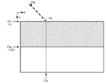
以下、表示装置1の動作例を説明する。ここでは、光変調器131が、WVGA相当の解像度を有する例を用いて説明する。すなわち、光変調器131は、480行800列の画素を有する(r=480、c=800)。オフセット最大値は120に設定されている(Omax=120)。VRAM121は、241行分のデータを記憶するための記憶領域を有する。なお、241行分とは、オフセット最大値(この例では120行)の2倍に、処理対象画素(この例では1行)の記憶領域を加算した値である。オフセットテーブル129は、各画素のオフセットベクトルを記憶している。
3. Operation Hereinafter, an operation example of the
3−1.概要
図8は、表示装置1の動作を示すフローチャートである。
3-1. Overview FIG. 8 is a flowchart showing the operation of the
ステップS101において、書き込みIF124は、画像データの一部を、VRAM121に書き込む。ここで書き込まれるデータは、オフセット最大値に相当する量のデータ、この例では、120行分のデータである。すなわち、書き込みIF124は、画像データのうち第1行から第120行までのデータを、VRAM121に書き込む。
In step S <b> 101, the writing IF 124 writes a part of the image data to the
VRAM121は、第1〜241行の記憶領域を有している。ステップS101においては、第1〜120行の記憶領域に画像データが書き込まれる。
The
ステップS102において、読み出しアドレス生成部125および書き込みIF124は、それぞれ、リードカウンターCrおよびライトカウンターCwを初期化する。この例では、Cr=1、Cw=Omax+Cr=121に初期化される。リードカウンターCrおよびライトカウンターCwは、画像データ上の行の位置を示すカウンターであり、この例では、いずれも1〜480の値をとる。なお、ライトカウンターCwとリードカウンターCrとの差は、少なくとも正方向側のオフセット最大値よりも大きい。
In step S102, the read
ステップS103において、読み出しアドレス生成部125および補正部127はxカウンターCxを初期化する。xカウンターCxは、処理対象の画素を特定するためのパラメーターである。読み出しアドレス生成部125および補正部127はそれぞれ個別にxカウンターCxを保持しているが、これらは同期信号で同期している。この例では、Cx=1に初期化される。以下、補正対象の画素を画素Pcと表す。画素Pcの座標は、(Cx,Cr)である。
In step S103, the read
ステップS104において、読み出しアドレス生成部125は、読み出しアドレスを生成する。画素Pcを基準としてオフセットベクトルVosが指す位置を、位置Pdと表す。位置Pdの座標(xd,yd)は、次式(4)で表される。
(xd,yd)=Pc+Vos …(4)
位置Pd(xd,yd)のデータは、VRAM121において、第kd行の記憶領域に記憶されている。読み出しアドレス生成部125は、次式(5)を用いて読み出しアドレスkdを計算する。
kd=yd(mod k) …(5)
例えば、k=241の場合においてyd=1〜241のときは、kd=ydである。yd=243の場合、kd=2である。
In step S104, the read
(Xd, yd) = Pc + Vos (4)
Data at the position Pd (xd, yd) is stored in the storage area of the kd-th row in the
kd = yd (mod k) (5)
For example, when k = 241 and yd = 1 to 241, kd = yd. In the case of yd = 243, kd = 2.
図9は、ステップS104における読み出しアドレス生成処理の詳細を示す図である。 FIG. 9 is a diagram showing details of the read address generation process in step S104.
ステップS1401において、読み出しアドレス生成部125は、参照画素を特定する。
In step S1401, the read
ステップS1402において、読み出しアドレス生成部125は、カウンターuを初期化する。カウンターuは、画素P1〜P4のうち対象となる画素を特定するカウンターである。ここではu=1に初期化される。
In step S1402, the read
ステップS1403において、読み出しアドレス生成部125は、画素Puのデータがキャッシュ1261に記憶されているか判断する。キャッシュ1261には、前回の補正に用いられた画素のデータが、その画素の座標とともに記憶されている。画素Puのデータがキャッシュ1261に記憶されていると判断された場合(S1403:YES)、読み出しアドレス生成部125は、処理をステップS1411に移行する。画素Puのデータがキャッシュ1261に記憶されていないと判断された場合(S1403:NO)、読み出しアドレス生成部125は、処理をステップS1404に移行する。
In step S1403, the
ステップS1404において、読み出しアドレス生成部125は、画素Puに対応する読み出しアドレスを生成する。読み出しアドレス生成部125は、次式(6)および(7)を用いて読み出しアドレスのx座標xrおよびy座標yr生成する。
xr=quotient(4,xu)−1 …(6)
yr=quotient(2,yu)−1 …(7)
なお、quotient(m,n)は、nをmで除した商を示す。
In step S1404, the
x r = quotient (4, x u) -1 ... (6)
y r = quatient (2, y u ) −1 (7)
Here, quotient (m, n) indicates a quotient obtained by dividing n by m.
ステップS1405において、読み出しアドレス生成部125は、以下の条件(8)〜(11)を用いて、画素Puのデータが記憶されているVRAMを特定する。
mod(xu 4)=0or1の場合、VRAM1211or1213 …(8)
mod(xu 4)=2or3の場合、VRAM1212or1214 …(9)
mod(yu 2)=0の場合、VRAM1211or1212 …(10)
mod(yu 2)=1の場合、VRAM1213or1214 …(11)
In step S1405, the read
When mod (x u 4) = 0 or 1, VRAM 1211 or 1213 (8)
When mod (x u 4) = 2 or 3, VRAM 1212 or 1214 (9)
mod the case of (y u 2) = 0, VRAM1211or1212 ... (10)
mod the case of (y u 2) = 1, VRAM1213or1214 ... (11)
ステップS1406において、読み出しアドレス生成部125は、読み出しアドレスで指定される単位記憶領域に含まれる参照画素の数を判断する。カウンターuが奇数の場合においてmod(xu 2)=0のときは、読み出しアドレス生成部125は、読み出しアドレス(xr,yr)で指定される単位記憶領域に、画素PuおよびPu+1の2つの参照画素のデータが含まれると判断する。カウンターuが奇数の場合においてmod(xu 2)=1のときは、読み出しアドレス生成部125は、読み出しアドレス(xr,yr)で指定される単位記憶領域に、1つの参照画素(画素Pu)のデータが含まれると判断する(残り1画素のデータは、補正には用いられない)。読み出しアドレス(xr,yr)で指定される単位記憶領域に含まれる参照画素の数が2つである場合(S1406:2)、読み出しアドレス生成部125は、処理をステップS1407に移行する。読み出しアドレス(xr,yr)で指定される単位記憶領域に含まれる参照画素の数が1つである場合(S1406:1)、読み出しアドレス生成部125は、処理をステップS1409に移行する。
In step S1406, the read
ステップS1407において、読み出しアドレス生成部125は、VRAM121に対しデータの読み出し要求を出力する。読み出し要求は、ステップS1405で特定されたVRAMに対して出力される。また、読み出し要求は、読み出しアドレスおよび画素P1〜P4のうちそのアドレスにデータが記憶されている2つの画素の識別子を含む。
In step S <b> 1407, the read
ステップS1408において、読み出しアドレス生成部125は、カウンターuを更新する。ここでは、u=u+2としてカウンターuを更新する。
In step S1408, the read
ステップS1409において、読み出しアドレス生成部125は、VRAM121に対しデータの読み出し要求を出力する。読み出し要求は、ステップS1405で特定されたVRAMに対して出力される。また、読み出し要求は、読み出しアドレスおよび画素P1〜P4のうちそのアドレスにデータが記憶されている1つの画素の識別子を含む。
In step S <b> 1409, the read
ステップS1410において、読み出しアドレス生成部125は、カウンターuを更新する。ここでは、u=u+1としてカウンターuを更新する。
In step S1410, the read
ステップS1411において、読み出しアドレス生成部125は、画素Puのデータがキャッシュ1261に記憶されている旨の情報を、読み出しIF126に出力する。
In step S1411, the read
ステップS1412において、読み出しアドレス生成部125は、画素P1〜P4の全てについて処理が完了したか判断する。画素P1〜P4の全てについて処理が完了したと判断された場合(S1412:YES)、読み出しアドレス生成部125は、ステップS104の処理を終了する。画素P1〜P4のうち処理されていない画素があると判断された場合(S1412:NO)、読み出しアドレス生成部125は、処理をステップS1403に移行する。
In step S1412, the read
再び図8を参照する。ステップS105において、読み出しIF126は、VRAM121からデータを取得する。ステップS1407またはS1409で読み出しアドレス生成部125から出力された読み出し要求は、アービター122を介してVRAM121に出力される。VRAM121は、指定されたアドレスの記憶領域からデータを読み出し、アービター122を介して読み出しIF126に出力する。
Refer to FIG. 8 again. In step S <b> 105, the read IF 126 acquires data from the
図10は、キャッシュ1261の構成を例示する図である。この例で、キャッシュ1261は、記憶領域1262および記憶領域1263を有する。記憶領域1262および記憶領域1263は、それぞれ、2行2列の4画素分のデータを記憶する。記憶領域1262および記憶領域1263の一方には前回の補正に用いられたデータが、他方には今回の補正に用いられるデータが記憶される。ここでは説明を簡単にするため、記憶領域1262に前回のデータが、記憶領域1263に今回のデータが記憶される例を説明する。
FIG. 10 is a diagram illustrating the configuration of the
読み出しIF126は、取得したデータから参照画素のデータを抽出する。VRAM121から出力されるデータには、そのデータに含まれる参照画素の識別子が付加されている。そのデータに参照画素P1およびP2のデータが含まれることが示されている場合、読み出しIF126は、上位24ビットのデータをP1のデータとして、下位24ビットをP2のデータとして抽出する。そのデータに参照画素P1のみのデータが含まれることが示されている場合、読み出しIF126は、下位24ビットのデータをP1のデータとして抽出する。そのデータに参照画素P2のみのデータが含まれることが示されている場合、読み出しIF126は、上位24ビットのデータをP2のデータとして抽出する。そのデータに参照画素P3およびP4のデータが含まれることが示されている場合、読み出しIF126は、上位24ビットのデータをP3のデータとして、下位24ビットをP4のデータとして抽出する。そのデータに参照画素P3のみのデータが含まれることが示されている場合、読み出しIF126は、下位24ビットのデータをP3のデータとして抽出する。そのデータに参照画素P4のみのデータが含まれることが示されている場合、読み出しIF126は、上位24ビットのデータをP4のデータとして抽出する。
The read-out IF 126 extracts reference pixel data from the acquired data. To the data output from the
読み出しIF126は、抽出した参照画素のデータを記憶領域1263に書き込む。
The read-out IF 126 writes the extracted reference pixel data in the
なお、キャッシュ1261に画素Puのデータが記憶されていることが読み出しアドレス生成部125から通知された場合、読み出しIF126は、記憶領域1262から画素Puのデータを読み出し、読み出したデータを記憶領域1263に書き込む。
Incidentally, when it is notified from the read
図9のフローで参照画素P1〜P4について処理が完了すると、それに応じて、記憶領域1263には参照画素P1〜P4のデータが書き込まれる。読み出しIF126は、記憶領域1263に記憶されているデータを、補正部127に出力する。その後、読み出しIF126は、記憶領域1263に記憶されているデータを、記憶領域1262にコピーする。
When the processing for the reference pixels P 1 to P 4 is completed in the flow of FIG. 9, the data of the reference pixels P 1 to P 4 is written in the
ステップS106において、補正部127は、式(2)を用いて画素Pcのデータを補正する。
In step S106, the
図11は、補正に用いられる画素を例示する図である。この例では、Pc=P(14,12)であり、Vos(14,12)=(−8,−10)である。式(4)から、
Pd=(6,2) …(12)
である。式(2)とあわせて、
Dr(14,12)=Do(6,2) …(13)
が得られる。
FIG. 11 is a diagram illustrating pixels used for correction. In this example, Pc = P (14,12) and Vos (14,12) = (− 8, −10). From equation (4)
Pd = (6,2) (12)
It is. Together with equation (2)
Dr (14,12) = Do (6,2) (13)
Is obtained.
再び図8を参照する。ステップS107において、映像出力部128は、補正部127により補正された画素Pcのデータを後段の回路(例えば光変調器131の駆動回路)に出力する。
Refer to FIG. 8 again. In step S107, the
ステップS108において、読み出しアドレス生成部125および補正部127は、xカウンターCxをインクリメントする。
In step S108, the read
ステップS109において、補正部127は、1行分の処理が完了したか、すなわち、Cx=801となったか判断する。まだ1行分の処理が完了していないと判断された場合(S109:NO)、補正部127は、処理をステップS104に移行する。1行分の処理が完了したと判断された場合(S109:YES)、補正部127は、処理をステップS110に移行する。
In step S109, the
ステップS110において、書き込みIF124は、ライトカウンターCwで指定される行のデータを、VRAM121に書き込む。ライトカウンターCwで指定される行のデータは、VRAM121において第kw行の記憶領域に書き込まれる。kwは次式(14)により計算される。
kw=Cw(mod k) …(14)
例えば、k=241の場合においてCw=1〜241のときは、kw=Cwである。Cw=243の場合、kw=2である。
In step S <b> 110, the write IF 124 writes the data of the row specified by the write counter Cw to the
kw = Cw (mod k) (14)
For example, when k = 241 and Cw = 1 to 241, kw = Cw. In the case of Cw = 243, kw = 2.
ステップS111において、読み出しアドレス生成部125および書き込みIF124は、カウンターCrおよびCwをインクリメントする。
In step S111, the read
ステップS112において、読み出しアドレス生成部125は、全ての行について処理が完了したか、すなわち、Cr=480となったか判断する。まだ全ての行について処理が完了していないと判断された場合(S112:NO)、読み出しアドレス生成部125は、処理をステップS103に移行する。全ての行について処理が完了したと判断された場合(S112:YES)、コントローラー12は、図8の処理を終了する。
In step S112, the read
なおここでは1枚(1フレーム)の画像のみを処理する例を説明したが、動画を処理する場合、複数フレームの画像を連続して処理してもよい。例えば、第iフレームについて処理をしている場合において、Cw>rとなったときは、ライトカウンターCwを初期化し、第(i+1)フレームのデータをVRAM121に書き込んでもよい。この場合において、Cr>rとなったときは、リードカウンターCrを初期化し、第(i+1)フレームのデータの処理を開始する。
In addition, although the example which processes only one image (one frame) was demonstrated here, when processing a moving image, you may process the image of several frames continuously. For example, when processing is performed for the i-th frame, when Cw> r, the write counter Cw may be initialized and the data of the (i + 1) -th frame may be written into the
以上で説明したように、本実施形態によれば、補正に用いられる画素を含む行を選択してラインバッファーに記憶する構成と比較して、処理の負荷を低減することができる。また、リードカウンターとライトカウンターとは同じスピードで行送りされるので、リードがライトを追い越す(書き込みが終わる前の画像データを誤って読み出してしまう)ことはない。 As described above, according to the present embodiment, it is possible to reduce the processing load as compared with a configuration in which a row including pixels used for correction is selected and stored in a line buffer. In addition, since the read counter and the write counter are advanced at the same speed, the read does not overtake the write (the image data before writing is not read in error).
また、本実施形態によれば、本発明を用いない構成(図1の例でコントローラー12を有さない構成)に対し、ホスト装置11と投写ユニット13(光変調器131)との間に本実施形態に係るコントローラー12を設ければよく、歪み補正に対応していないシステムに簡単に低コストで歪み補正の機能を導入することができる。
In addition, according to the present embodiment, a configuration that does not use the present invention (a configuration that does not include the
3−2.動作例
以下、より具体的な動作例を説明する。
3-2. Operation Example Hereinafter, a more specific operation example will be described.
3−2−1.データ読み出しの例
ここでは、VRAM1211〜1214からのデータの読み出しの例を説明する。
3-2-1. Data Reading Example Here, an example of reading data from the VRAMs 1211 to 1214 will be described.
3−2−1−1.動作例1
図12は動作例1を示す図である。この例では、参照画素P1〜P4が、(0,0)、(1,0)、(0,1)、および(1,1)である例を説明する。なおこの例では、キャッシュ1261に参照画素のデータは記憶されていない。この場合、VRAM1211の単位記憶領域A(0,0)およびVRAM1213の単位記憶領域A(0,0)から読み出したデータを用いて補正が行われる。図において、読み出されるデータには丸印が付されている。
3-2-1-1. Operation example 1
FIG. 12 is a diagram illustrating the first operation example. In this example, an example in which the reference pixels P 1 to P 4 are (0, 0), (1, 0), (0, 1), and (1, 1) will be described. In this example, reference pixel data is not stored in the
3−2−1−2.動作例2
図13は動作例2を示す図である。この例では、参照画素P1〜P4が、(1,0)、(2,0)、(1,1)、および(2,1)である例を説明する。なおこの例では、キャッシュ1261に参照画素のデータは記憶されていない。この場合、VRAM1211の単位記憶領域A(0,0)、VRAM1212の単位記憶領域A(0,0)、VRAM1213の単位記憶領域A(0,0)、およびVRAM1214の単位記憶領域A(0,0)から読み出したデータを用いて補正が行われる。
3-2-1-2. Operation example 2
FIG. 13 is a diagram illustrating the second operation example. In this example, an example in which the reference pixels P 1 to P 4 are (1, 0), (2, 0), (1, 1), and (2, 1) will be described. In this example, reference pixel data is not stored in the
3−2−1−3.動作例3
図14は動作例3を示す図である。この例では、参照画素P1〜P4が、(3,1)、(4,1)、(3,2)、および(4,2)である例を説明する。なおこの例では、キャッシュ1261に参照画素のデータは記憶されていない。この場合、VRAM1211の単位記憶領域A(1,1)、VRAM1212の単位記憶領域A(0,1)、VRAM1213の単位記憶領域A(1,0)、およびVRAM1214の単位記憶領域A(0,0)から読み出したデータを用いて補正が行われる。
3-2-1-3. Operation example 3
FIG. 14 is a diagram illustrating the third operation example. In this example, an example in which the reference pixels P 1 to P 4 are (3, 1), (4, 1), (3, 2), and (4, 2) will be described. In this example, reference pixel data is not stored in the
3−2−1−4.動作例4
図15は動作例4を示す図である。この例では、前回補正時の参照画素P1〜P4が、(0,0)、(1,0)、(0,1)、および(1,1)であり、かつ、今回補正時の参照画素P1〜P4が、(1,0)、(2,0)、(1,1)、(2,1)である。キャッシュ1261には、画素(0,0)、(1,0)、(0,1)、および(1,1)のデータが記憶されている。この場合、VRAM1212の単位記憶領域A(0,0)およびVRAM1214の単位記憶領域A(0,0)から読み出したデータ、並びにキャッシュ1261に記憶されているデータが用いられる。この場合、VRAM121へ2回アクセスすれば、補正に用いられるデータを得ることができる。
3-2-1-4. Operation example 4
FIG. 15 is a diagram illustrating the fourth operation example. In this example, the reference pixels P 1 to P 4 at the previous correction are (0, 0), (1, 0), (0, 1), and (1, 1), and at the time of the current correction. The reference pixels P 1 to P 4 are (1, 0), (2, 0), (1, 1), and (2, 1). The
オフセットベクトルは画素毎に定義されるが、隣り合う画素でオフセットベクトルが大きく異なることは少ない。すなわち、今回補正時の参照画素は、前回補正時の参照画素から1画素分だけ移動しているケースがほとんどである。したがって、キャッシュ1261を用いることにより、VRAM121へのアクセス回数を大幅に低減することができる。
Although the offset vector is defined for each pixel, the offset vector is rarely greatly different between adjacent pixels. That is, in most cases, the reference pixel at the current correction is moved by one pixel from the reference pixel at the previous correction. Therefore, by using the
3−2−1−5.動作例5
この例では、参照画素P1〜P4が、(0,−1)、(1,−1)、(0,0)、および(1,0)である例を説明する。すなわち、参照画素P1およびP2は、元の画像データ(以下「元データ」という)の範囲外の画素である。元データの範囲外の画素のデータとしては、所定値のデータが用いられる。所定値のデータは、読み出しIF126内のレジスター(図示略)に記憶されている。参照画素が元データの範囲外であった場合、読み出しアドレス生成部125は、その旨を読み出しIF126に通知する。
3-2-1-5. Operation example 5
In this example, an example in which the reference pixels P 1 to P 4 are (0, −1), (1, −1), (0, 0), and (1, 0) will be described. That is, the reference pixels P 1 and P 2 are pixels outside the range of the original image data (hereinafter referred to as “original data”). Data of a predetermined value is used as pixel data outside the range of the original data. The predetermined value data is stored in a register (not shown) in the read IF 126. If the reference pixel is outside the range of the original data, the read
3−2−1−6.動作例6
この例では、参照画素P1〜P4が、(0,−2)、(1,−2)、(0,−1)、および(1,−1)である例を説明する。すなわち、すべての参照画素が元データの範囲外の画素である。すべての参照画素が元データの範囲外であった場合、読み出しアドレス生成部125は、その旨を読み出し補正部127に通知する。この場合、補正部127は、補正(補間演算)を行わず、所定値をそのまま処理対象画素のデータとして出力する。
3-2-1-6. Operation example 6
In this example, the
なお、動作例4〜6のように、キャッシュ1261またはレジスターからデータを読み出している期間はアービター122からVRAM121にアクセスしていないので、他の装置(例えばホスト装置11)からVRAM121にアクセスすることができる。
As in the operation examples 4 to 6, since the
3−2−2.VRAM121へのデータ書き込み/読み出しの例
ここでは、VRAM121に対するデータの書き込みおよび読み出しの例を説明する。ここでは説明の便宜上、VRAM1211〜1214を区別せず、単一のVRAM121として説明する。
3-2-2. Example of Data Writing / Reading to VRAM 121 Here, an example of data writing / reading to / from the
図16は、Cr=1およびCw=121の状態(ステップS107)を示す図である。図は、VRAM121の状態を示している。ハッチングされた部分は、第1〜120行のデータが記憶されていることを示している。白抜きの部分は、データが記憶されていない(ヌル値が記憶されている)ことを示している。
FIG. 16 is a diagram illustrating a state where Cr = 1 and Cw = 121 (step S107). The figure shows the state of the
この例で、オフセットベクトルVos(Pc)のx成分およびy成分はともに負である。すなわち、参照画素は元データにおいて存在しない画素である。この場合、補正部127は、補正後のデータを所定の値(例えばヌル値または黒に相当する階調)にする。図16では便宜的に、VosおよびPdを破線で示し、元データにおいて存在しない画素を参照していることを示している。
In this example, the x component and the y component of the offset vector Vos (Pc) are both negative. That is, the reference pixel is a pixel that does not exist in the original data. In this case, the
図17は、Cr=120およびCw=241の状態(ステップS107)を示す図である。このとき、VRAM121の第1〜241行の記憶領域には、画像の第1〜241行のデータが記憶されている。
FIG. 17 is a diagram illustrating a state where Cr = 120 and Cw = 241 (step S107). At this time, the data of the first to 241th rows of the image is stored in the storage area of the first to 241th rows of the
図18は、Cr=200およびCw=321の状態(ステップS107)を示す図である。このとき、VRAM121の第1〜80行の記憶領域には、画像の第242〜321行のデータが記憶されている。VRAM121の第81〜241行の記憶領域には、画像の第81〜241行のデータが記憶されている。この例で、Pc=(300,200)、Vos(Pc)=(20,100)である。これらを式(4)に代入して
Pd=(320,300) …(15)
が得られる。式(5)から
kd=59 …(16)
であるので、参照画素Puのデータは、VRAM121の第59行の記憶領域に記憶されている。
FIG. 18 is a diagram illustrating a state where Cr = 200 and Cw = 321 (step S107). At this time, the storage areas of the 1st to 80th lines of the
Is obtained. From equation (5), kd = 59 (16)
Since it is, the data of the reference pixel P u is stored in a storage area of the first 59 rows of
VRAM121においては、リードカウンターの進行方向に対し正方向および負方向の双方において、オフセット最大値分の行数のデータが記憶されているので、補正に用いるデータを読み出すことができる。
In the
4.変形例
本発明は上述の実施形態に限定されるものではなく、種々の変形実施が可能である。以下、変形例をいくつか説明する。以下の変形例のうち2つ以上のものが組み合わせて用いられてもよい。
4). Modifications The present invention is not limited to the above-described embodiments, and various modifications can be made. Hereinafter, some modifications will be described. Two or more of the following modifications may be used in combination.
4−1.変形例1
VRAM121に含まれるフレームバッファーの数は4つに限定されない。例えば、VRAM121は、2つのフレームバッファーを有していてもよい。
4-1.
The number of frame buffers included in the
図19は、2つのフレームバッファー(VRAM1211およびVRAM1212)を用いる場合の記憶領域の割り当てを例示する図である。VRAM1211の単位記憶領域A(s,t)には、画素P(2s,2t)および画素P(2s+1,2t)のデータが記憶される。VRAM1212の単位記憶領域A(s,t)には、画素P(2s,2t+1)および画素P(2s+1,2t+1)のデータが記憶される。 FIG. 19 is a diagram illustrating allocation of storage areas when two frame buffers (VRAM 1211 and VRAM 1212) are used. In the unit storage area A (s, t) of the VRAM 1211, data of the pixel P (2s, 2t) and the pixel P (2s + 1, 2t) are stored. In the unit storage area A (s, t) of the VRAM 1212, data of the pixel P (2s, 2t + 1) and the pixel P (2s + 1, 2t + 1) are stored.
この場合、参照画素P1〜P4が例えば、(1,0)、(2,0)、(1,1)、および(2,1)であった場合、単一のフレームバッファーに順次2回アクセスする必要がある。すなわち、データの読み出しに2クロックを要する。しかし、フレームバッファーの分割数が少なくなるため、回路規模をより縮小できる。 In this case, when the reference pixels P 1 to P 4 are, for example, (1, 0), (2, 0), (1, 1), and (2, 1), 2 are sequentially added to a single frame buffer. Need to access once. That is, two clocks are required for reading data. However, since the number of frame buffer divisions is reduced, the circuit scale can be further reduced.
また、VRAM121は複数のフレームバッファーを含まず、単一のフレームバッファーとして機能してもよい。
The
4−2.変形例2
補正に用いられる参照画素の数は4つに限定されない。例えば、オフセットベクトルが指す位置Pdの周辺m行n列の(m×n)個の画素が参照画素として用いられてもよい。例えば、オフセットベクトルが指す位置Pdの周辺4行4列の16個の画素が参照画素として用いられてもよい。
4-2.
The number of reference pixels used for correction is not limited to four. For example, (m × n) pixels in m rows and n columns around the position Pd pointed to by the offset vector may be used as reference pixels. For example, 16 pixels of 4 rows and 4 columns around the position Pd pointed to by the offset vector may be used as the reference pixels.
4−3.変形例3
VRAM121の記憶容量は、k行分に限定されない。1フレームの全画素分、すなわちr行分の記憶領域を有していてもよい。この場合、VRAM121の容量は大きくなるが、リードカウンターおよびライトカウンターによる読み出しおよび書き込みの制御は不要になる。
4-3.
The storage capacity of the
4−4.変形例4
オフセットベクトルが指す位置Pdが、パッキングされていない2つの画素の間に入った場合、パッキングされた2つの画素の間に位置Pdをずらす補正が行われてもよい。この補正がなければVRAM121に4回のアクセスが必要であるが、この補正をすればVRAM121へのアクセスは2回で済む。
4-4.
When the position Pd pointed to by the offset vector enters between two unpacked pixels, a correction for shifting the position Pd between the two packed pixels may be performed. Without this correction, the
図20は、変形例4に係る位置Pdの補正を例示する図である。点Xが補正前の位置Pdを、点Yが補正後の位置Pdを示している。 FIG. 20 is a diagram illustrating correction of the position Pd according to the fourth modification. Point X indicates a position Pd before correction, and point Y indicates a position Pd after correction.
また、図19の例において、位置Pdが、パッキングされていない2つの画素の間に入った場合、パッキングされた2つの画素の間に位置Pdをずらす補正が行われてもよい。この補正をすれば、1つのフレームバッファーへのアクセスは1回で済むので1クロックでデータを読み出すことができる。 In the example of FIG. 19, when the position Pd enters between two unpacked pixels, correction for shifting the position Pd between the two packed pixels may be performed. With this correction, data can be read out in one clock because one frame buffer needs to be accessed only once.
4−5.変形例5
読み出しIF126はキャッシュ1261を有していなくてもよい。
4-5. Modification 5
The read IF 126 may not have the
4−6.変形例6
オフセットベクトルVosは、理論的には全ての画素P(x,y)について定義することが可能であるが全ての画素P(x,y)についてオフセットベクトルを記憶すると多くのメモリー容量が必要になる場合には、記憶しておくオフセットベクトルを間引いてもよい。例えば、行方向および列方向ともに2画素毎にオフセットベクトルをオフセットテーブル129に記憶しておくと、3行3列の9個の画素のうち4隅の画素のみオフセットベクトルが記憶されていることになる。このとき、オフセットベクトルが記憶されていない画素に関しては、近接する、オフセットベクトルが記憶されている画素のオフセットベクトルを用いた補間により、その画素のオフセットベクトルを算出する。
4-6. Modification 6
The offset vector Vos can theoretically be defined for all the pixels P (x, y), but if the offset vector is stored for all the pixels P (x, y), a large memory capacity is required. In this case, the stored offset vector may be thinned out. For example, if the offset vector is stored in the offset table 129 for every two pixels in both the row direction and the column direction, the offset vector is stored only in the four corner pixels of the nine pixels in the third row and the third column. Become. At this time, for a pixel for which no offset vector is stored, the offset vector of the pixel is calculated by interpolation using the offset vector of the adjacent pixel in which the offset vector is stored.
例えば、Vos(1,1)=(p1,q1)およびVos(1,3)=(p2,q2)がオフセットテーブル129に記憶されており、Vos(1,2)がオフセットテーブル129に記憶されていないときは、
Vos(1,2)={Vos(1,1)+Vos(1,3)}/2
=[{(p1+p2)/2},{(q1+q2)/2}] …(17)
によりVos(1,2)が算出される。
For example, Vos (1,1) = (p1, q1) and Vos (1,3) = (p2, q2) are stored in the offset table 129, and Vos (1,2) is stored in the offset table 129. When not
Vos (1,2) = {Vos (1,1) + Vos (1,3)} / 2
= [{(P1 + p2) / 2}, {(q1 + q2) / 2}] (17)
Thus, Vos (1, 2) is calculated.
4−7.変形例7
VRAM121の記憶容量は、実施形態で説明したものに限定されない。例えば、オフセット最大値がリードカウンターの進行方向に対して正方向および負方向の双方について個別に設定されていた場合、正方向のオフセット最大値、負方向のオフセット最大値、および処理対象画素の記憶領域を加算した値に相当する行数の記憶領域を有していてもよい。具体的には、正方向のオフセット最大値O+max=120、負方向のオフセット最大値O−max=80、処理対象の画素数が1の場合、VRAM121は、201(=120+80+1)行分の記憶領域を有していればよい。このとき、ライトカウンターCwの値は、次式(18)のように、リードカウンターCrに対して、負方向のオフセット最大値分ずらしておけばよい。
Cw=Cr+O−max …(18)
4-7. Modification 7
The storage capacity of the
Cw = Cr + O − max (18)
4−8.他の変形例
表示装置1はHUDに限定されない。表示装置1は、いわゆる通常のプロジェクターであってもよい。この場合において、プロジェクターのキーストーン補正に本発明が適用されてもよい。特に、いわゆるピコプロジェクターのような小型のプロジェクターにおいて有効である。
4-8. Other Modifications The
表示装置1および表示装置1の各部の構成は、図1および図2で例示したものに限定されない。実施形態では、ハードウェア(コントローラー12)が図8のフローを実行する例を説明したが、ホスト装置11のCPU111が、プログラムに従って図8のフローを実行してもよい。この場合、コントローラー12は無くてもよい。また、実施形態においてはリードカウンターおよびライトカウンターが読み出しアドレス生成部125および書き込みIF124のレジスターに記憶される例を説明したが、これらのカウンターはVRAM121等、他の記憶装置に記憶されてもよい。
The configurations of the
CPU111が実行するプログラムは、磁気記録媒体(磁気テープ、磁気ディスク(HDD、FD(Flexible Disk))など)、光記録媒体(光ディスク(CD(Compact Disk)、DVD(Digital Versatile Disk))など)、光磁気記録媒体、半導体メモリ(フラッシュROMなど)などのコンピューター読取り可能な記録媒体に記憶した状態で提供されてもよい。また、このプログラムは、インターネットのようなネットワーク経由でダウンロードされてもよい。
The programs executed by the
本発明は、表示装置以外の電子機器、例えば撮像装置に適用されてもよい。例えば、デジタルスチルカメラ、デジタルビデオカメラ、ドライブレコーダーにおける補正に、本発明が適用されてもよい。 The present invention may be applied to electronic equipment other than a display device, for example, an imaging device. For example, the present invention may be applied to correction in a digital still camera, a digital video camera, and a drive recorder.
1…表示装置、11…ホスト装置、111…CPU、112…ROM、113…RAM、12…コントローラー、121…VRAM、1211…VRAM、1212…VRAM、1213…VRAM、1214…VRAM、122…アービター、123…映像入力部、124…書き込みIF、125…読み出しアドレス生成部、126…読み出しIF、1261…キャッシュ、127…補正部、128…映像出力部、129…オフセットテーブル、13…投写ユニット、131…光変調器、14…記憶部、15…IF部、16…操作パネル、181…表示領域、182…長方形、1821〜1824…頂点、183…図形、1831〜1834…点、184…図形、1841〜1844…点、185…図形、1851〜1854…点
DESCRIPTION OF
Claims (7)
前記画像のうちk1行分のデータに相当する複数の記憶領域を有し、当該複数の記憶領域の各々に、隣り合う少なくとも2画素のデータを記憶する第1記憶部と、
前記画像のうちk2行分(k1およびk2は、Omax<(k1+k2)<rを満たす自然数であり、Omaxは前記表示部に対してあらかじめ設定されたオフセット最大値である)のデータに相当する複数の記憶領域を有し、当該複数の記憶領域の各々に、前記第1記憶部にデータが記憶されている画素とは異なる行において隣り合う少なくとも2画素のデータを記憶する第2記憶部と、
前記r行c列の画素のうち処理対象となる対象画素のデータを、前記第1記憶部および前記第2記憶部において当該対象画素に対応するオフセットベクトルにより示される位置に対応する記憶領域に記憶されている複数の画素のデータを用いて補正を行う補正部と
を有し、
前記画像の少なくとも一部が1行おきに、互い違いに、前記第1記憶部および前記第2記憶部に分割されて記憶される
画像処理装置。 An image processing apparatus that processes an image displayed on a display unit having pixels of r rows and c columns,
A first storage unit having a plurality of storage areas corresponding to data for k1 rows of the image, and storing data of at least two adjacent pixels in each of the plurality of storage areas;
A plurality of data corresponding to k2 lines of the image (k1 and k2 are natural numbers satisfying Omax <(k1 + k2) <r, and Omax is a maximum offset value set in advance for the display unit). A second storage unit that stores data of at least two pixels adjacent to each other in a row different from the pixels in which data is stored in the first storage unit,
Data of a target pixel to be processed among the pixels in the r row and c column is stored in a storage area corresponding to a position indicated by an offset vector corresponding to the target pixel in the first storage unit and the second storage unit. using data of a plurality of pixels that are to have a correction unit that performs correction,
An image processing apparatus in which at least a part of the image is alternately divided and stored in the first storage unit and the second storage unit every other row .
ことを特徴とする請求項1に記載の画像処理装置。 When the position indicated by the offset vector is a position between a pixel stored in the first storage area of the first storage unit and a pixel stored in the second storage area of the second storage unit, The image processing apparatus according to claim 1, wherein the correction unit performs the correction using data stored in the first storage area and the second storage area.
ことを特徴とする請求項1または2に記載の画像処理装置。 When the position indicated by the offset vector corresponds to a position between two pixels stored in the two storage areas of the first storage unit, the correction unit sequentially reads from the two storage areas. The image processing apparatus according to claim 1, wherein the correction is performed using the processed data.
前記対象画素が、前記直近の単位期間から1画素分移動した場合、前記補正部は、前記キャッシュ記憶部に記憶されているデータ、並びに前記第1記憶部および前記第2記憶部のいずれかに記憶されているデータを用いて前記補正を行う
ことを特徴とする請求項1ないし3のいずれか一項に記載の画像処理装置。 A cache storage unit for storing data used by the correction unit in the most recent unit period;
When the target pixel has moved by one pixel from the most recent unit period, the correction unit stores data stored in the cache storage unit, and one of the first storage unit and the second storage unit. The image processing apparatus according to claim 1, wherein the correction is performed using stored data.
前記第2記憶部にデータが記憶されている画素と同じ行において当該画素と隣り合う画素を含み、互いに隣り合う少なくとも2画素のデータを記憶する第4記憶部と
を有し、
前記画像の一部が2列おきに、互い違いに、前記第1記憶部および前記第3記憶部に分割されて記憶され、
前記画像の残りが2列おきに、互い違いに、前記第2記憶部および前記第4記憶部に分割されて記憶され、
前記補正部は、前記対象画素のデータを、前記第1記憶部、前記第2記憶部、前記第3記憶部、および前記第4記憶部において当該対象画素に対応するオフセットベクトルにより示される位置に対応する記憶領域に記憶されている複数の画素のデータを用いて前記補正を行う
ことを特徴とする請求項1ないし4のいずれか一項に記載の画像処理装置。 A third storage unit that stores data of at least two pixels adjacent to each other, including a pixel adjacent to the pixel in the same row as the pixel in which data is stored in the first storage unit;
A fourth storage unit that stores data of at least two pixels adjacent to each other, including pixels adjacent to the pixel in the same row as the pixels in which data is stored in the second storage unit;
A part of the image is stored in two rows, alternately divided into the first storage unit and the third storage unit,
The rest of the image is stored in two rows alternately, divided into the second storage unit and the fourth storage unit,
The correction unit moves the data of the target pixel to a position indicated by an offset vector corresponding to the target pixel in the first storage unit, the second storage unit, the third storage unit, and the fourth storage unit. The image processing apparatus according to any one of claims 1 to 4, wherein the correction is performed using data of a plurality of pixels stored in a corresponding storage area.
前記表示部に表示される画像のうちk1行分のデータに相当する複数の記憶領域を有し、当該複数の記憶領域の各々に、隣り合う少なくとも2画素のデータを記憶する第1記憶部と、
前記画像のうちk2行分(k1およびk2は、Omax<(k1+k2)<rを満たす自然数であり、Omaxは前記表示部に対してあらかじめ設定されたオフセット最大値である)のデータに相当する複数の記憶領域を有し、当該複数の記憶領域の各々に、前記第1記憶部にデータが記憶されている画素とは異なる行において隣り合う少なくとも2画素のデータを記憶する第2記憶部と、
前記r行c列の画素のうち処理対象となる対象画素のデータを、前記第1記憶部および前記第2記憶部において当該対象画素に対応するオフセットベクトルにより示される位置に対応する記憶領域に記憶されている複数の画素のデータを用いて補正を行う補正部と
を有し、
前記画像の少なくとも一部が1行おきに、互い違いに、前記第1記憶部および前記第2記憶部に分割されて記憶される
表示装置。 a display unit having pixels of r rows and c columns;
A first storage unit having a plurality of storage areas corresponding to data for k1 rows of the image displayed on the display unit, and storing data of at least two adjacent pixels in each of the plurality of storage areas; ,
A plurality of data corresponding to k2 lines of the image (k1 and k2 are natural numbers satisfying Omax <(k1 + k2) <r, and Omax is a maximum offset value set in advance for the display unit). A second storage unit that stores data of at least two pixels adjacent to each other in a row different from the pixels in which data is stored in the first storage unit,
Data of a target pixel to be processed among the pixels in the r row and c column is stored in a storage area corresponding to a position indicated by an offset vector corresponding to the target pixel in the first storage unit and the second storage unit. using data of a plurality of pixels that are to have a correction unit that performs correction,
A display device in which at least a part of the image is alternately divided and stored in the first storage unit and the second storage unit every other row .
前記画像のうちk1行分のデータに相当する複数の記憶領域を有し、当該複数の記憶領域の各々に、隣り合う少なくとも2画素のデータを第1記憶部に記憶するステップと、
前記画像のうちk2行分(k1およびk2は、Omax<(k1+k2)<rを満たす自然数であり、Omaxは前記表示部に対してあらかじめ設定されたオフセット最大値である)のデータに相当する複数の記憶領域を有し、当該複数の記憶領域の各々に、前記第1記憶部にデータが記憶されている画素とは異なる行において隣り合う少なくとも2画素のデータを第2記憶部に記憶するステップと、
前記r行c列の画素のうち処理対象となる対象画素のデータを、前記第1記憶部および前記第2記憶部において当該対象画素に対応するオフセットベクトルにより示される位置に対応する記憶領域に記憶されている複数の画素のデータを用いて補正を行うステップと
を有し、
前記画像の少なくとも一部が1行おきに、互い違いに、前記第1記憶部および前記第2記憶部に分割されて記憶される
画像処理方法。 An image processing method for processing an image displayed on a display unit having pixels of r rows and c columns,
Having a plurality of storage areas corresponding to k1 rows of data in the image, and storing data of at least two adjacent pixels in each of the plurality of storage areas in the first storage unit;
A plurality of data corresponding to k2 lines of the image (k1 and k2 are natural numbers satisfying Omax <(k1 + k2) <r, and Omax is a maximum offset value set in advance for the display unit). A step of storing, in each of the plurality of storage areas, data of at least two pixels adjacent to each other in a row different from the pixels in which data is stored in the first storage unit in the second storage unit When,
Data of a target pixel to be processed among the pixels in the r row and c column is stored in a storage area corresponding to a position indicated by an offset vector corresponding to the target pixel in the first storage unit and the second storage unit. possess and performing a correction using the data of a plurality of pixels being,
An image processing method in which at least a part of the image is alternately divided and stored in the first storage unit and the second storage unit every other row .
Priority Applications (3)
| Application Number | Priority Date | Filing Date | Title |
|---|---|---|---|
| JP2014112522A JP6361290B2 (en) | 2014-05-30 | 2014-05-30 | Image processing apparatus, display apparatus, and image processing method |
| US14/719,914 US9336565B2 (en) | 2014-05-30 | 2015-05-22 | Image processing device, display apparatus, and image processing method |
| CN201510289890.7A CN105323519A (en) | 2014-05-30 | 2015-05-29 | Image processing device, display apparatus, and image processing method |
Applications Claiming Priority (1)
| Application Number | Priority Date | Filing Date | Title |
|---|---|---|---|
| JP2014112522A JP6361290B2 (en) | 2014-05-30 | 2014-05-30 | Image processing apparatus, display apparatus, and image processing method |
Publications (3)
| Publication Number | Publication Date |
|---|---|
| JP2015228056A JP2015228056A (en) | 2015-12-17 |
| JP2015228056A5 JP2015228056A5 (en) | 2017-06-29 |
| JP6361290B2 true JP6361290B2 (en) | 2018-07-25 |
Family
ID=54702403
Family Applications (1)
| Application Number | Title | Priority Date | Filing Date |
|---|---|---|---|
| JP2014112522A Expired - Fee Related JP6361290B2 (en) | 2014-05-30 | 2014-05-30 | Image processing apparatus, display apparatus, and image processing method |
Country Status (3)
| Country | Link |
|---|---|
| US (1) | US9336565B2 (en) |
| JP (1) | JP6361290B2 (en) |
| CN (1) | CN105323519A (en) |
Families Citing this family (4)
| Publication number | Priority date | Publication date | Assignee | Title |
|---|---|---|---|---|
| JP5924020B2 (en) * | 2012-02-16 | 2016-05-25 | セイコーエプソン株式会社 | Projector and projector control method |
| US11240475B2 (en) | 2018-04-17 | 2022-02-01 | Sony Corporation | Information processing apparatus and method |
| CN112130325B (en) * | 2020-09-25 | 2022-07-12 | 东风汽车有限公司 | Parallax correction system and method for vehicle-mounted head-up display, storage medium and electronic device |
| JP2023046936A (en) * | 2021-09-24 | 2023-04-05 | シャープディスプレイテクノロジー株式会社 | Display device and manufacturing method of display device |
Family Cites Families (22)
| Publication number | Priority date | Publication date | Assignee | Title |
|---|---|---|---|---|
| JP2702930B2 (en) * | 1987-06-29 | 1998-01-26 | 株式会社日立製作所 | Filtering method |
| JPH03154175A (en) | 1989-11-13 | 1991-07-02 | Toshiba Corp | Picture storage device |
| JPH0844862A (en) | 1994-07-29 | 1996-02-16 | Sony Corp | Image processor |
| JPH08138039A (en) | 1994-11-10 | 1996-05-31 | Sumitomo Metal Ind Ltd | Semiconductor memory, affine transformation method for picture, picture processor, and address generation circuit |
| JPH09147097A (en) | 1995-11-27 | 1997-06-06 | Matsushita Electric Ind Co Ltd | Data interpolating device |
| JPH09311934A (en) | 1996-05-24 | 1997-12-02 | Sharp Corp | Image processor |
| JP3133702B2 (en) | 1997-05-30 | 2001-02-13 | 三洋電機株式会社 | Digital still camera |
| JP4021566B2 (en) | 1998-07-30 | 2007-12-12 | 株式会社日立コミュニケーションテクノロジー | Data memory device and data memory control method |
| JP4313863B2 (en) | 1998-09-11 | 2009-08-12 | 株式会社タイトー | Image processing device |
| JP3633807B2 (en) | 1998-12-16 | 2005-03-30 | 松下電器産業株式会社 | Intermediate pixel arithmetic unit |
| JP4019757B2 (en) | 2002-03-15 | 2007-12-12 | 富士ゼロックス株式会社 | Storage device |
| JP3843902B2 (en) * | 2002-07-11 | 2006-11-08 | セイコーエプソン株式会社 | Projector to correct keystone distortion |
| JP4432786B2 (en) | 2005-01-28 | 2010-03-17 | カシオ計算機株式会社 | Camera device and image processing method |
| JP5227502B2 (en) * | 2006-09-15 | 2013-07-03 | 株式会社半導体エネルギー研究所 | Liquid crystal display device driving method, liquid crystal display device, and electronic apparatus |
| JP5117762B2 (en) * | 2007-05-18 | 2013-01-16 | 株式会社半導体エネルギー研究所 | Liquid crystal display |
| JP2009236955A (en) * | 2008-03-25 | 2009-10-15 | Seiko Epson Corp | Projector |
| JP5556234B2 (en) * | 2010-02-25 | 2014-07-23 | セイコーエプソン株式会社 | VIDEO PROCESSING CIRCUIT, ITS PROCESSING METHOD, LIQUID CRYSTAL DISPLAY DEVICE, AND ELECTRONIC DEVICE |
| JP5744418B2 (en) * | 2010-05-18 | 2015-07-08 | キヤノン株式会社 | Projection apparatus and projection method |
| JP2012019338A (en) | 2010-07-07 | 2012-01-26 | Renesas Electronics Corp | Semiconductor device |
| CN102156969B (en) * | 2011-04-12 | 2013-09-25 | 潘林岭 | Processing method for correcting deviation of image |
| JP5958079B2 (en) * | 2012-05-22 | 2016-07-27 | 株式会社Jvcケンウッド | Projection apparatus, image correction method, and program |
| JP6201290B2 (en) * | 2012-10-02 | 2017-09-27 | セイコーエプソン株式会社 | Image display device and image adjustment method of image display device |
-
2014
- 2014-05-30 JP JP2014112522A patent/JP6361290B2/en not_active Expired - Fee Related
-
2015
- 2015-05-22 US US14/719,914 patent/US9336565B2/en active Active
- 2015-05-29 CN CN201510289890.7A patent/CN105323519A/en active Pending
Also Published As
| Publication number | Publication date |
|---|---|
| JP2015228056A (en) | 2015-12-17 |
| US20150348267A1 (en) | 2015-12-03 |
| CN105323519A (en) | 2016-02-10 |
| US9336565B2 (en) | 2016-05-10 |
Similar Documents
| Publication | Publication Date | Title |
|---|---|---|
| JP2591770B2 (en) | Comprehensive distortion correction in real-time image generation systems | |
| JP6361290B2 (en) | Image processing apparatus, display apparatus, and image processing method | |
| CN102196223B (en) | Image processing method in projector, projective transformation processing means and projector | |
| WO2017140438A1 (en) | A method of stabilizing a sequence of images | |
| US8928782B2 (en) | Image processing device and image capture device | |
| CN109360229B (en) | Laser projection image processing method, device and equipment | |
| US20160337639A1 (en) | Projection apparatus | |
| JP6427961B2 (en) | Image processing apparatus, display apparatus, image processing method, and program | |
| US20150193915A1 (en) | Technique for projecting an image onto a surface with a mobile device | |
| JP5348035B2 (en) | projector | |
| CN109634032B (en) | Image processing method and device | |
| US10657622B2 (en) | Controlling projected image frame rate in response to determined projection surface curvature | |
| JP5533109B2 (en) | Image display device, projector, and data acquisition method in image display device | |
| JP2018088669A (en) | Projection image distortion correction device and method | |
| US8509568B2 (en) | Image processing apparatus and image processing method | |
| JP2012230302A (en) | Image generation device, projection type image display device, image display system, image generation method and computer program | |
| JP2005208413A (en) | Image processor and image display device | |
| JP2013061420A (en) | Projector and image processing device | |
| JP6648985B2 (en) | Image processing apparatus and image processing method | |
| JP2002278507A (en) | Image processor and image display device | |
| US11114001B2 (en) | Image processing device, method of controlling image processing device, and display device | |
| JP4266150B2 (en) | Projection apparatus and projection method | |
| JP5353772B2 (en) | projector | |
| JP6064699B2 (en) | Image processing apparatus, projector, and image processing method | |
| JP2018133772A (en) | Image processing device and image processing method |
Legal Events
| Date | Code | Title | Description |
|---|---|---|---|
| A521 | Request for written amendment filed |
Free format text: JAPANESE INTERMEDIATE CODE: A523 Effective date: 20170522 |
|
| A621 | Written request for application examination |
Free format text: JAPANESE INTERMEDIATE CODE: A621 Effective date: 20170522 |
|
| A131 | Notification of reasons for refusal |
Free format text: JAPANESE INTERMEDIATE CODE: A131 Effective date: 20180320 |
|
| A521 | Request for written amendment filed |
Free format text: JAPANESE INTERMEDIATE CODE: A523 Effective date: 20180517 |
|
| TRDD | Decision of grant or rejection written | ||
| A01 | Written decision to grant a patent or to grant a registration (utility model) |
Free format text: JAPANESE INTERMEDIATE CODE: A01 Effective date: 20180529 |
|
| A61 | First payment of annual fees (during grant procedure) |
Free format text: JAPANESE INTERMEDIATE CODE: A61 Effective date: 20180611 |
|
| R150 | Certificate of patent or registration of utility model |
Ref document number: 6361290 Country of ref document: JP Free format text: JAPANESE INTERMEDIATE CODE: R150 |
|
| LAPS | Cancellation because of no payment of annual fees |