JP2015228056A5 - - Google Patents
Download PDFInfo
- Publication number
- JP2015228056A5 JP2015228056A5 JP2014112522A JP2014112522A JP2015228056A5 JP 2015228056 A5 JP2015228056 A5 JP 2015228056A5 JP 2014112522 A JP2014112522 A JP 2014112522A JP 2014112522 A JP2014112522 A JP 2014112522A JP 2015228056 A5 JP2015228056 A5 JP 2015228056A5
- Authority
- JP
- Japan
- Prior art keywords
- storage area
- data
- vram
- pixel
- stored
- Prior art date
- Legal status (The legal status is an assumption and is not a legal conclusion. Google has not performed a legal analysis and makes no representation as to the accuracy of the status listed.)
- Granted
Links
- 238000000034 method Methods 0.000 description 2
- 230000000051 modifying Effects 0.000 description 2
- 230000003287 optical Effects 0.000 description 2
- 230000004048 modification Effects 0.000 description 1
- 238000006011 modification reaction Methods 0.000 description 1
Images
Description
VRAM121の各々において、第j行第i列の単位記憶領域をA(i,j)と表すと、VRAM1211の単位記憶領域A(s,t)には、画素P(4s,2t)および画素P(4s+1,2t)のデータが記憶される。VRAM1212の単位記憶領域A(s,t)には、画素P(4s+2,2t)および画素P(4s+3,2t)のデータが記憶される。VRAM1213の単位記憶領域A(s,t)には、画素P(4s,2t+1)および画素P(4s+1,2t+1)のデータが記憶される。VRAM1214の単位記憶領域A(s,t)には、画素P(4s+2,2t+1)および画素P(4s+3,2t+1)のデータが記憶される。 In each VRAM 121, when the unit storage area in the j-th row and the i-th column is represented as A (i, j), the unit storage area A (s, t) of the VRAM 1211 includes the pixel P (4s, 2t) and the pixel P. Data of (4s + 1, 2t) is stored. In the unit storage area A (s, t) of the VRAM 1212, data of the pixel P (4s + 2, 2t) and the pixel P (4s + 3, 2t) are stored. In the unit storage area A (s, t) of the VRAM 1213, data of the pixel P (4s, 2t + 1) and the pixel P (4s + 1, 2t + 1) are stored. VRAM121 4 of unit storage area A (s, t), the data of the pixel P (4s + 2,2t + 1) and pixel P (4s + 3,2t + 1) is stored.
例えば、参照画素P1〜P4が、(3,1)、(4,1)、(3,2)、および(4,2)の間にあった場合、VRAM1211の単位記憶領域A(1,1)に記憶されているデータ(P(4,2)およびP(5,2)のデータ)、VRAM1212の単位記憶領域A(0,1)に記憶されているデータ(P(2,2)およびP(3,2)のデータ)、VRAM1213の単位記憶領域A(1,0)に記憶されているデータ(P(4,1)およびP(5,1)のデータ)、およびVRAM1214の単位記憶領域A(0,0)に記憶されているデータ(P(2,1)およびP(3,1)のデータ)が読み出される。この場合は、メモリーへのアクセスは4回である。 For example, when the reference pixels P1 to P4 are between (3, 1), (4, 1), (3, 2), and (4, 2), the unit storage area A (1, 1) of the VRAM 1211 is stored. Stored data (data of P (4, 2 ) and P (5, 2 )), data stored in the unit storage area A (0, 1) of the VRAM 1212 (P (2, 2) and P ( 3, 2)), data stored in the unit storage area A (1,0) of the VRAM 1213 (data of P (4, 1 ) and P (5, 1 )), and unit storage area A of the VRAM 1214 Data (P (2,1) and P (3,1) data) stored in (0,0) is read. In this case, the memory is accessed four times.
3.動作
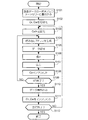
以下、表示装置1の動作例を説明する。ここでは、光変調器131が、WVGA相当の解像度を有する例を用いて説明する。すなわち、光変調器131は、480行800列の画素を有する(r=480、c=800)。オフセット最大値は120に設定されている(Omax=120)。VRAM121は、241行分のデータを記憶するための記憶領域を有する。なお、241行分とは、オフセット最大値(この例では120行)の2倍に、処理対象画素(この例では1行)の記憶領域を加算した値である。オフセットテーブル129は、各画素のオフセットベクトルを記憶している。
3. Operation Hereinafter, an operation example of the display device 1 will be described. Here, an example in which the optical modulator 131 has a resolution equivalent to WVGA will be described. In other words, the optical modulator 131 has 480 rows and 800 columns of pixels (r = 480, c = 800). The maximum offset value is set to 120 (Omax = 120). The VRAM 121 has a storage area for storing 241 rows of data. The 241 rows are values obtained by adding the storage area of the pixel to be processed (1 row in this example) to twice the maximum offset value (120 rows in this example). The offset table 129 stores an offset vector of each pixel.
ステップS109において、補正部127は、1行分の処理が完了したか、すなわち、Cx=801となったか判断する。まだ1行分の処理が完了していないと判断された場合(S109:NO)、補正部127は、処理をステップS104に移行する。1行分の処理が完了したと判断された場合(S109:YES)、補正部127は、処理をステップS110に移行する。 In step S109, the correction unit 127 determines whether the processing for one row is completed, that is, whether Cx = 801. When it is determined that the process for one line has not been completed (S109: NO), the correction unit 127 shifts the process to step S104. If the processing of one line is determined to be completed (S109: YES), the correction unit 127, the flow goes to step S11 0.
4−7.変形例7
VRAM121の記憶容量は、実施形態で説明したものに限定されない。例えば、オフセット最大値がリードカウンターの進行方向に対して正方向および負方向の双方について個別に設定されていた場合、正方向のオフセット最大値、負方向のオフセット最大値、および処理対象画素の記憶領域を加算した値に相当する行数の記憶領域を有していてもよい。具体的には、正方向のオフセット最大値O+max=120、負方向のオフセット最大値O−max=80、処理対象の画素数が1の場合、VRAM121は、201(=120+80+1)行分の記憶領域を有していればよい。このとき、ライトカウンターCwの値は、次式(18)のように、リードカウンターCrに対して、負方向のオフセット最大値分ずらしておけばよい。
Cw=Cr+O−max …(18)
4-7. Modification 7
The storage capacity of the VRAM 121 is not limited to that described in the embodiment. For example, when the offset maximum value is set separately for both the positive direction and the negative direction with respect to the traveling direction of the lead counter, the positive offset maximum value, the negative offset maximum value, and the processing target pixel are stored. You may have a storage area of the number of lines equivalent to the value which added the area | region. Specifically, when the maximum offset value in the positive direction O + max = 120, the maximum offset value in the negative direction O − max = 80, and the number of pixels to be processed is 1, the VRAM 121 stores 201 (= 120 + 80 + 1) rows. It only needs to have a storage area. At this time, the value of the write counter Cw may be shifted by the maximum offset value in the negative direction with respect to the read counter Cr as shown in the following equation (1 8 ).
Cw = Cr + O − max (18)
Priority Applications (3)
| Application Number | Priority Date | Filing Date | Title |
|---|---|---|---|
| JP2014112522A JP6361290B2 (en) | 2014-05-30 | 2014-05-30 | Image processing apparatus, display apparatus, and image processing method |
| US14/719,914 US9336565B2 (en) | 2014-05-30 | 2015-05-22 | Image processing device, display apparatus, and image processing method |
| CN201510289890.7A CN105323519A (en) | 2014-05-30 | 2015-05-29 | Image processing device, display apparatus, and image processing method |
Applications Claiming Priority (1)
| Application Number | Priority Date | Filing Date | Title |
|---|---|---|---|
| JP2014112522A JP6361290B2 (en) | 2014-05-30 | 2014-05-30 | Image processing apparatus, display apparatus, and image processing method |
Publications (3)
| Publication Number | Publication Date |
|---|---|
| JP2015228056A JP2015228056A (en) | 2015-12-17 |
| JP2015228056A5 true JP2015228056A5 (en) | 2017-06-29 |
| JP6361290B2 JP6361290B2 (en) | 2018-07-25 |
Family
ID=54702403
Family Applications (1)
| Application Number | Title | Priority Date | Filing Date |
|---|---|---|---|
| JP2014112522A Expired - Fee Related JP6361290B2 (en) | 2014-05-30 | 2014-05-30 | Image processing apparatus, display apparatus, and image processing method |
Country Status (3)
| Country | Link |
|---|---|
| US (1) | US9336565B2 (en) |
| JP (1) | JP6361290B2 (en) |
| CN (1) | CN105323519A (en) |
Families Citing this family (4)
| Publication number | Priority date | Publication date | Assignee | Title |
|---|---|---|---|---|
| JP5924020B2 (en) * | 2012-02-16 | 2016-05-25 | セイコーエプソン株式会社 | Projector and projector control method |
| WO2019203002A1 (en) * | 2018-04-17 | 2019-10-24 | ソニー株式会社 | Information processing device and method |
| CN112130325B (en) * | 2020-09-25 | 2022-07-12 | 东风汽车有限公司 | Parallax correction system and method for vehicle-mounted head-up display, storage medium and electronic device |
| JP2023046936A (en) * | 2021-09-24 | 2023-04-05 | シャープディスプレイテクノロジー株式会社 | Display device and manufacturing method of display device |
Family Cites Families (22)
| Publication number | Priority date | Publication date | Assignee | Title |
|---|---|---|---|---|
| JP2702930B2 (en) * | 1987-06-29 | 1998-01-26 | 株式会社日立製作所 | Filtering method |
| JPH03154175A (en) | 1989-11-13 | 1991-07-02 | Toshiba Corp | Picture storage device |
| JPH0844862A (en) | 1994-07-29 | 1996-02-16 | Sony Corp | Image processor |
| JPH08138039A (en) | 1994-11-10 | 1996-05-31 | Sumitomo Metal Ind Ltd | Semiconductor memory, affine transformation method for picture, picture processor, and address generation circuit |
| JPH09147097A (en) | 1995-11-27 | 1997-06-06 | Matsushita Electric Ind Co Ltd | Data interpolating device |
| JPH09311934A (en) | 1996-05-24 | 1997-12-02 | Sharp Corp | Image processor |
| JP3133702B2 (en) | 1997-05-30 | 2001-02-13 | 三洋電機株式会社 | Digital still camera |
| JP4021566B2 (en) | 1998-07-30 | 2007-12-12 | 株式会社日立コミュニケーションテクノロジー | Data memory device and data memory control method |
| JP4313863B2 (en) | 1998-09-11 | 2009-08-12 | 株式会社タイトー | Image processing device |
| JP3633807B2 (en) | 1998-12-16 | 2005-03-30 | 松下電器産業株式会社 | Intermediate pixel arithmetic unit |
| JP4019757B2 (en) | 2002-03-15 | 2007-12-12 | 富士ゼロックス株式会社 | Storage device |
| JP3843902B2 (en) * | 2002-07-11 | 2006-11-08 | セイコーエプソン株式会社 | Projector to correct keystone distortion |
| JP4432786B2 (en) | 2005-01-28 | 2010-03-17 | カシオ計算機株式会社 | Camera device and image processing method |
| JP5227502B2 (en) * | 2006-09-15 | 2013-07-03 | 株式会社半導体エネルギー研究所 | Liquid crystal display device driving method, liquid crystal display device, and electronic apparatus |
| JP5117762B2 (en) * | 2007-05-18 | 2013-01-16 | 株式会社半導体エネルギー研究所 | Liquid crystal display |
| JP2009236955A (en) * | 2008-03-25 | 2009-10-15 | Seiko Epson Corp | Projector |
| JP5556234B2 (en) * | 2010-02-25 | 2014-07-23 | セイコーエプソン株式会社 | VIDEO PROCESSING CIRCUIT, ITS PROCESSING METHOD, LIQUID CRYSTAL DISPLAY DEVICE, AND ELECTRONIC DEVICE |
| JP5744418B2 (en) * | 2010-05-18 | 2015-07-08 | キヤノン株式会社 | Projection apparatus and projection method |
| JP2012019338A (en) | 2010-07-07 | 2012-01-26 | Renesas Electronics Corp | Semiconductor device |
| CN102156969B (en) * | 2011-04-12 | 2013-09-25 | 潘林岭 | Processing method for correcting deviation of image |
| JP5958079B2 (en) * | 2012-05-22 | 2016-07-27 | 株式会社Jvcケンウッド | Projection apparatus, image correction method, and program |
| JP6201290B2 (en) * | 2012-10-02 | 2017-09-27 | セイコーエプソン株式会社 | Image display device and image adjustment method of image display device |
-
2014
- 2014-05-30 JP JP2014112522A patent/JP6361290B2/en not_active Expired - Fee Related
-
2015
- 2015-05-22 US US14/719,914 patent/US9336565B2/en active Active
- 2015-05-29 CN CN201510289890.7A patent/CN105323519A/en active Pending
Similar Documents
| Publication | Publication Date | Title |
|---|---|---|
| JP2015228056A5 (en) | ||
| MY182446A (en) | Region identifying operation for identfying region of a memory attribute unit corresponding to a target memory address | |
| JP2010096864A5 (en) | ||
| WO2016023003A3 (en) | Failure mapping in a storage array | |
| JP2016086306A5 (en) | ||
| JP2016190089A5 (en) | ||
| JP2016032623A5 (en) | ||
| WO2016022993A3 (en) | Adjustable error correction based on memory health in a storage unit | |
| JP2015128537A5 (en) | ||
| JP2018046985A5 (en) | ||
| RU2017137745A (en) | CONSUMPTION COMPONENTS FOR IMAGE FORMATION | |
| MY193452A (en) | Image loading method and device | |
| US9007279B2 (en) | Controlling one or more displays | |
| WO2015112148A3 (en) | Atomically committing write requests | |
| JP2017070380A5 (en) | ||
| JP2016082358A5 (en) | ||
| EP4242975A3 (en) | Image processing method and display apparatus therefor | |
| EP3273390A3 (en) | Hardware implementation of a temporal memory system | |
| JP2015227913A5 (en) | ||
| JP2017083625A5 (en) | Display driver and display device | |
| US20150293786A1 (en) | Method for processing cr algorithm by actively utilizing shared memory of multi-processor, and processor using the same | |
| JP2015201672A5 (en) | ||
| JP2020081277A5 (en) | ||
| JP2017117402A5 (en) | ||
| WO2016034421A3 (en) | Device and process for improving efficiency of image rendering |