JP6337026B2 - 基板貫通ビア(tsv)を備えた容量性微細加工超音波トランスデューサ(cumt)デバイス - Google Patents
基板貫通ビア(tsv)を備えた容量性微細加工超音波トランスデューサ(cumt)デバイス Download PDFInfo
- Publication number
- JP6337026B2 JP6337026B2 JP2015560307A JP2015560307A JP6337026B2 JP 6337026 B2 JP6337026 B2 JP 6337026B2 JP 2015560307 A JP2015560307 A JP 2015560307A JP 2015560307 A JP2015560307 A JP 2015560307A JP 6337026 B2 JP6337026 B2 JP 6337026B2
- Authority
- JP
- Japan
- Prior art keywords
- thin film
- substrate
- cumt
- layer
- transducer
- Prior art date
- Legal status (The legal status is an assumption and is not a legal conclusion. Google has not performed a legal analysis and makes no representation as to the accuracy of the status listed.)
- Active
Links
- 239000000758 substrate Substances 0.000 title claims description 81
- 239000010409 thin film Substances 0.000 claims description 61
- 239000002184 metal Substances 0.000 claims description 39
- 229910052751 metal Inorganic materials 0.000 claims description 39
- 239000010949 copper Substances 0.000 claims description 14
- 229910021421 monocrystalline silicon Inorganic materials 0.000 claims description 8
- 238000002161 passivation Methods 0.000 claims description 6
- RYGMFSIKBFXOCR-UHFFFAOYSA-N Copper Chemical compound [Cu] RYGMFSIKBFXOCR-UHFFFAOYSA-N 0.000 claims description 5
- 229910052802 copper Inorganic materials 0.000 claims description 5
- 239000010408 film Substances 0.000 claims description 5
- 239000012528 membrane Substances 0.000 claims description 5
- 210000004027 cell Anatomy 0.000 claims 12
- 239000011231 conductive filler Substances 0.000 claims 7
- 210000001744 T-lymphocyte Anatomy 0.000 claims 4
- 239000002210 silicon-based material Substances 0.000 claims 3
- 239000000945 filler Substances 0.000 claims 1
- 238000000034 method Methods 0.000 description 37
- 230000008569 process Effects 0.000 description 19
- XUIMIQQOPSSXEZ-UHFFFAOYSA-N Silicon Chemical compound [Si] XUIMIQQOPSSXEZ-UHFFFAOYSA-N 0.000 description 18
- 239000000463 material Substances 0.000 description 18
- 229910052710 silicon Inorganic materials 0.000 description 18
- 239000010703 silicon Substances 0.000 description 18
- VYPSYNLAJGMNEJ-UHFFFAOYSA-N Silicium dioxide Chemical compound O=[Si]=O VYPSYNLAJGMNEJ-UHFFFAOYSA-N 0.000 description 15
- 238000004519 manufacturing process Methods 0.000 description 14
- 229910052814 silicon oxide Inorganic materials 0.000 description 13
- 238000005530 etching Methods 0.000 description 12
- 230000000873 masking effect Effects 0.000 description 8
- 230000003647 oxidation Effects 0.000 description 6
- 238000007254 oxidation reaction Methods 0.000 description 6
- 229910016570 AlCu Inorganic materials 0.000 description 5
- 230000004888 barrier function Effects 0.000 description 5
- 238000000059 patterning Methods 0.000 description 5
- 239000004065 semiconductor Substances 0.000 description 4
- 238000002604 ultrasonography Methods 0.000 description 4
- 241000724291 Tobacco streak virus Species 0.000 description 3
- 238000003491 array Methods 0.000 description 3
- 238000004140 cleaning Methods 0.000 description 3
- 239000013078 crystal Substances 0.000 description 3
- 238000000151 deposition Methods 0.000 description 3
- 230000008021 deposition Effects 0.000 description 3
- 238000004806 packaging method and process Methods 0.000 description 3
- 239000007787 solid Substances 0.000 description 3
- MHAJPDPJQMAIIY-UHFFFAOYSA-N Hydrogen peroxide Chemical compound OO MHAJPDPJQMAIIY-UHFFFAOYSA-N 0.000 description 2
- 230000008901 benefit Effects 0.000 description 2
- 230000005540 biological transmission Effects 0.000 description 2
- 239000000356 contaminant Substances 0.000 description 2
- 230000008878 coupling Effects 0.000 description 2
- 238000010168 coupling process Methods 0.000 description 2
- 238000005859 coupling reaction Methods 0.000 description 2
- 238000000708 deep reactive-ion etching Methods 0.000 description 2
- 238000009792 diffusion process Methods 0.000 description 2
- 230000003628 erosive effect Effects 0.000 description 2
- 238000000227 grinding Methods 0.000 description 2
- 238000002844 melting Methods 0.000 description 2
- 230000008018 melting Effects 0.000 description 2
- 238000001465 metallisation Methods 0.000 description 2
- 238000012858 packaging process Methods 0.000 description 2
- 229920002120 photoresistant polymer Polymers 0.000 description 2
- 238000005498 polishing Methods 0.000 description 2
- WGTYBPLFGIVFAS-UHFFFAOYSA-M tetramethylammonium hydroxide Chemical compound [OH-].C[N+](C)(C)C WGTYBPLFGIVFAS-UHFFFAOYSA-M 0.000 description 2
- 239000010936 titanium Substances 0.000 description 2
- XLYOFNOQVPJJNP-UHFFFAOYSA-N water Substances O XLYOFNOQVPJJNP-UHFFFAOYSA-N 0.000 description 2
- 238000001039 wet etching Methods 0.000 description 2
- VHUUQVKOLVNVRT-UHFFFAOYSA-N Ammonium hydroxide Chemical compound [NH4+].[OH-] VHUUQVKOLVNVRT-UHFFFAOYSA-N 0.000 description 1
- 238000009623 Bosch process Methods 0.000 description 1
- 241000587161 Gomphocarpus Species 0.000 description 1
- BPQQTUXANYXVAA-UHFFFAOYSA-N Orthosilicate Chemical compound [O-][Si]([O-])([O-])[O-] BPQQTUXANYXVAA-UHFFFAOYSA-N 0.000 description 1
- 229910052581 Si3N4 Inorganic materials 0.000 description 1
- BOTDANWDWHJENH-UHFFFAOYSA-N Tetraethyl orthosilicate Chemical compound CCO[Si](OCC)(OCC)OCC BOTDANWDWHJENH-UHFFFAOYSA-N 0.000 description 1
- RTAQQCXQSZGOHL-UHFFFAOYSA-N Titanium Chemical compound [Ti] RTAQQCXQSZGOHL-UHFFFAOYSA-N 0.000 description 1
- 239000000853 adhesive Substances 0.000 description 1
- 230000001070 adhesive effect Effects 0.000 description 1
- 229910045601 alloy Inorganic materials 0.000 description 1
- 239000000956 alloy Substances 0.000 description 1
- 239000000908 ammonium hydroxide Substances 0.000 description 1
- 238000000137 annealing Methods 0.000 description 1
- 238000011109 contamination Methods 0.000 description 1
- VYQRBKCKQCRYEE-UHFFFAOYSA-N ctk1a7239 Chemical compound C12=CC=CC=C2N2CC=CC3=NC=CC1=C32 VYQRBKCKQCRYEE-UHFFFAOYSA-N 0.000 description 1
- 239000003989 dielectric material Substances 0.000 description 1
- 239000003814 drug Substances 0.000 description 1
- 238000009713 electroplating Methods 0.000 description 1
- 239000007789 gas Substances 0.000 description 1
- XLYOFNOQVPJJNP-UHFFFAOYSA-M hydroxide Chemical compound [OH-] XLYOFNOQVPJJNP-UHFFFAOYSA-M 0.000 description 1
- 238000003384 imaging method Methods 0.000 description 1
- 238000007654 immersion Methods 0.000 description 1
- 239000012212 insulator Substances 0.000 description 1
- 238000012804 iterative process Methods 0.000 description 1
- 150000002739 metals Chemical class 0.000 description 1
- 150000004767 nitrides Chemical class 0.000 description 1
- 238000000206 photolithography Methods 0.000 description 1
- 238000000678 plasma activation Methods 0.000 description 1
- 238000001020 plasma etching Methods 0.000 description 1
- 238000007747 plating Methods 0.000 description 1
- 230000004044 response Effects 0.000 description 1
- 239000000523 sample Substances 0.000 description 1
- 239000000377 silicon dioxide Substances 0.000 description 1
- 235000012239 silicon dioxide Nutrition 0.000 description 1
- HQVNEWCFYHHQES-UHFFFAOYSA-N silicon nitride Chemical compound N12[Si]34N5[Si]62N3[Si]51N64 HQVNEWCFYHHQES-UHFFFAOYSA-N 0.000 description 1
- 125000006850 spacer group Chemical group 0.000 description 1
- 239000000126 substance Substances 0.000 description 1
- 230000003746 surface roughness Effects 0.000 description 1
- 229910052719 titanium Inorganic materials 0.000 description 1
Images


Classifications
-
- B—PERFORMING OPERATIONS; TRANSPORTING
- B06—GENERATING OR TRANSMITTING MECHANICAL VIBRATIONS IN GENERAL
- B06B—METHODS OR APPARATUS FOR GENERATING OR TRANSMITTING MECHANICAL VIBRATIONS OF INFRASONIC, SONIC, OR ULTRASONIC FREQUENCY, e.g. FOR PERFORMING MECHANICAL WORK IN GENERAL
- B06B1/00—Methods or apparatus for generating mechanical vibrations of infrasonic, sonic, or ultrasonic frequency
- B06B1/02—Methods or apparatus for generating mechanical vibrations of infrasonic, sonic, or ultrasonic frequency making use of electrical energy
- B06B1/0292—Electrostatic transducers, e.g. electret-type
-
- A—HUMAN NECESSITIES
- A61—MEDICAL OR VETERINARY SCIENCE; HYGIENE
- A61B—DIAGNOSIS; SURGERY; IDENTIFICATION
- A61B8/00—Diagnosis using ultrasonic, sonic or infrasonic waves
- A61B8/44—Constructional features of the ultrasonic, sonic or infrasonic diagnostic device
- A61B8/4483—Constructional features of the ultrasonic, sonic or infrasonic diagnostic device characterised by features of the ultrasound transducer
-
- H—ELECTRICITY
- H02—GENERATION; CONVERSION OR DISTRIBUTION OF ELECTRIC POWER
- H02N—ELECTRIC MACHINES NOT OTHERWISE PROVIDED FOR
- H02N1/00—Electrostatic generators or motors using a solid moving electrostatic charge carrier
- H02N1/002—Electrostatic motors
-
- H—ELECTRICITY
- H02—GENERATION; CONVERSION OR DISTRIBUTION OF ELECTRIC POWER
- H02N—ELECTRIC MACHINES NOT OTHERWISE PROVIDED FOR
- H02N1/00—Electrostatic generators or motors using a solid moving electrostatic charge carrier
- H02N1/002—Electrostatic motors
- H02N1/006—Electrostatic motors of the gap-closing type
- H02N1/008—Laterally driven motors, e.g. of the comb-drive type
-
- B—PERFORMING OPERATIONS; TRANSPORTING
- B06—GENERATING OR TRANSMITTING MECHANICAL VIBRATIONS IN GENERAL
- B06B—METHODS OR APPARATUS FOR GENERATING OR TRANSMITTING MECHANICAL VIBRATIONS OF INFRASONIC, SONIC, OR ULTRASONIC FREQUENCY, e.g. FOR PERFORMING MECHANICAL WORK IN GENERAL
- B06B2201/00—Indexing scheme associated with B06B1/0207 for details covered by B06B1/0207 but not provided for in any of its subgroups
- B06B2201/70—Specific application
- B06B2201/76—Medical, dental
Landscapes
- Health & Medical Sciences (AREA)
- Life Sciences & Earth Sciences (AREA)
- Engineering & Computer Science (AREA)
- Biomedical Technology (AREA)
- Medical Informatics (AREA)
- Gynecology & Obstetrics (AREA)
- Biophysics (AREA)
- Nuclear Medicine, Radiotherapy & Molecular Imaging (AREA)
- Pathology (AREA)
- Radiology & Medical Imaging (AREA)
- Mechanical Engineering (AREA)
- Heart & Thoracic Surgery (AREA)
- Physics & Mathematics (AREA)
- Molecular Biology (AREA)
- Surgery (AREA)
- Animal Behavior & Ethology (AREA)
- General Health & Medical Sciences (AREA)
- Public Health (AREA)
- Veterinary Medicine (AREA)
- Transducers For Ultrasonic Waves (AREA)
- Pressure Sensors (AREA)
- Internal Circuitry In Semiconductor Integrated Circuit Devices (AREA)
- Micromachines (AREA)
Description
Claims (20)
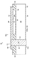
- 容量性微細加工超音波トランスデューサ(CMUT)セルを含むCMUTデバイスであって、
前記CMUTセルが、
頂部側と底部側とを含む基板と、
前記基板の頂部側の上の誘電体層であって、第1の領域と、前記第1の領域により横方向に囲まれて前記第1の領域よりも薄い第2の領域とを含み、前記第1及び第2の領域がキャビティを定める、前記誘電体層と、
前記誘電体層の第1の領域上に直接に接合され、前記誘電体層の第2の領域の上で前記キャビティを取り囲む薄膜層であって、前記キャビティ内に可動薄膜を含む、前記薄膜層と、
前記基板と前記誘電体層と前記薄膜層とに入り込み、前記可動薄膜から横方向に離れて位置する基板貫通ビア(TSV)であって、前記薄膜層と共面になるように、前記基板の底部側から延在する導電性充填材を含む、前記基板貫通ビア(TSV)と、
前記基板の頂部側の上で前記導電性充填材に接する金属層であって、前記薄膜層に沿って横方向に延び、前記可動薄膜に接する、前記金属層と、
を含む、デバイス。 - 請求項1に記載のCMUTデバイスであって、
前記金属層の上の誘電性パッシベーション層を更に含む、デバイス。 - 請求項1に記載のCMUTデバイスであって、
第2のCMUTセルと、
前記基板の底部側の下の前記第1のCMUTセルの前記導電性充填材に接して前記第1のCMUTセルを前記第2のCMUTセルに接続する第2の金属層と、
を更に含む、デバイス。 - 請求項1に記載のCMUTデバイスであって、
前記薄膜層が単結晶シリコン材料を含む、デバイス。 - 請求項1に記載のCMUTデバイスであって、
前記導電性充填材が、銅を含み、前記基板の前記底部側から突出する、デバイス。 - 請求項1に記載のCMUTデバイスであって、
前記基板が、0.1Ω−cmより小さいか又はそれに等しい抵抗を有する、デバイス。 - 請求項1に記載のCMUTデバイスであって、
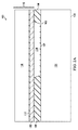
前記薄膜層が前記誘電体層に真空融解ボンディングされる、デバイス。 - トランスデューサデバイスであって、
第1の側と第1の側の反対の第2の側とを有する基板と、
トランスデューサセルと、
を含み、
前記トランスデューサセルが、
前記基板の第1の側の上の誘電体層であって、第1の領域と、第1の領域よりも薄く、キャビティを定めるために前記第1の領域により横方向に囲まれる第2の領域とを有する、前記誘電体層と、
前記キャビティを取り囲み、前記誘電体層の第2の領域の上に可動薄膜を含む薄膜層と、
前記基板と前記誘電体層と前記薄膜層とに入り込む貫通基板ビア(TSV)と、
を含む、デバイス。 - 請求項8に記載のトランスデューサデバイスであって、
前記薄膜層が前記誘電体層の第1の領域上に直接に接合される、デバイス。 - 請求項8に記載のトランスデューサデバイスであって、
前記TSVが、前記可動薄膜に垂直に重なっていない、デバイス。 - 請求項8に記載のトランスデューサデバイスであって、
前記TSVが、前記薄膜層と共面になるように前記基板の第2の側から延びる導電性充填材を含む、デバイス。 - 請求項8に記載のトランスデューサデバイスであって、
前記基板の第1の側に隣接する前記TSVに接する金属層であって、前記薄膜層に沿って横方向に延び、前記可動薄膜に接する、前記金属層を更に含む、デバイス。 - 請求項8に記載のトランスデューサデバイスであって、
前記薄膜層が単結晶シリコン材料を含む、デバイス。 - 請求項8に記載のトランスデューサデバイスであって、
第2のトランスデューサセルと、
前記第2のトランスデューサセルを前記基板の第2の側に隣接する前記トランスデューサセルの前記TSVに接続する金属層と、
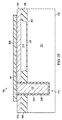
を更に含む、デバイス。 - トランスデューサデバイスであって、
第1の側と前記第1の側の反対の第2の側とを有する基板と、
複数のトランスデューサセルであって、各トランスデューサセルが、
前記基板の第1の側の上の誘電体層であって、第1の領域と、前記第1の領域よりも薄く、キャビティを定めるように前記第1の領域により横方向に囲まれる第2の領域とを有する、前記誘電体層と、
前記キャビティを取り囲む薄膜層であって、前記誘電体層の第2の領域の上に可動薄膜を含む、前記薄膜層と、
前記基板と前記誘電体層と前記薄膜層とに入り込む貫通基板ビア(TSV)であって、誘電体充填材を含む、前記TSVと、
を含む、前記複数のトランスデューサセルと、
前記基板の第2の側に隣接する少なくとも2つの前記トランスデューサセルの導電性充填材に接続する相互接続金属層と、
を含む、デバイス。 - 請求項15に記載のトランスデューサデバイスであって、
前記薄膜層が前記誘電体層の第1の領域に直接に接合される、デバイス。 - 請求項15に記載のトランスデューサデバイスであって、
前記TSVが、前記可動薄膜に垂直に重ならない、デバイス。 - 請求項15に記載のトランスデューサデバイスであって、
前記導電性充填材が、前記薄膜層と共面となるように前記基板の第2の側から延びる、デバイス。 - 請求項15に記載のトランスデューサデバイスであって、
前記基板の第1の側に隣接する前記TSVに接する相互セル金属層であって、前記薄膜層に沿って横方向に延び、前記可動薄膜に接する、前記相互セル金属層を更に含む、デバイス。 - 請求項15に記載のトランスデューサデバイスであって、
前記薄膜層が単結晶シリコン材料を含む、デバイス。
Applications Claiming Priority (3)
| Application Number | Priority Date | Filing Date | Title |
|---|---|---|---|
| US13/779,376 US9520811B2 (en) | 2013-02-27 | 2013-02-27 | Capacitive micromachined ultrasonic transducer (CMUT) device with through-substrate via (TSV) |
| US13/779,376 | 2013-02-27 | ||
| PCT/US2014/019011 WO2014134301A1 (en) | 2013-02-27 | 2014-02-27 | Capacitive micromachined ultrasonic transducer (cmut) device with through-substrate via (tsv) |
Publications (3)
| Publication Number | Publication Date |
|---|---|
| JP2016511607A JP2016511607A (ja) | 2016-04-14 |
| JP2016511607A5 JP2016511607A5 (ja) | 2017-04-06 |
| JP6337026B2 true JP6337026B2 (ja) | 2018-06-06 |
Family
ID=51387424
Family Applications (1)
| Application Number | Title | Priority Date | Filing Date |
|---|---|---|---|
| JP2015560307A Active JP6337026B2 (ja) | 2013-02-27 | 2014-02-27 | 基板貫通ビア(tsv)を備えた容量性微細加工超音波トランスデューサ(cumt)デバイス |
Country Status (4)
| Country | Link |
|---|---|
| US (2) | US9520811B2 (ja) |
| JP (1) | JP6337026B2 (ja) |
| CN (1) | CN105025802B (ja) |
| WO (1) | WO2014134301A1 (ja) |
Families Citing this family (16)
| Publication number | Priority date | Publication date | Assignee | Title |
|---|---|---|---|---|
| US9470710B2 (en) | 2013-02-27 | 2016-10-18 | Texas Instruments Incorporated | Capacitive MEMS sensor devices |
| US9351081B2 (en) * | 2013-02-27 | 2016-05-24 | Texas Instruments Incorporated | Capacitive micromachined ultrasonic transducer (CMUT) with through-substrate via (TSV) substrate plug |
| US9520811B2 (en) * | 2013-02-27 | 2016-12-13 | Texas Instruments Incorporated | Capacitive micromachined ultrasonic transducer (CMUT) device with through-substrate via (TSV) |
| JP6221582B2 (ja) * | 2013-09-30 | 2017-11-01 | セイコーエプソン株式会社 | 超音波デバイスおよびプローブ並びに電子機器および超音波画像装置 |
| US9761509B2 (en) * | 2015-12-29 | 2017-09-12 | United Microelectronics Corp. | Semiconductor device with throgh-substrate via and method for fabrication the semiconductor device |
| CA3052485A1 (en) * | 2017-02-27 | 2018-08-30 | Butterfly Network, Inc. | Capacitive micromachined ultrasonic transducers (cmuts) and related apparatus and methods |
| US10662055B2 (en) | 2017-04-27 | 2020-05-26 | Seiko Epson Corporation | MEMS element, sealing structure, electronic device, electronic apparatus, and vehicle |
| KR102450580B1 (ko) | 2017-12-22 | 2022-10-07 | 삼성전자주식회사 | 금속 배선 하부의 절연층 구조를 갖는 반도체 장치 |
| CN112004611A (zh) * | 2018-03-09 | 2020-11-27 | 蝴蝶网络有限公司 | 超声换能器装置以及制造超声换能器装置的方法 |
| WO2020100112A1 (en) * | 2018-11-16 | 2020-05-22 | Vermon S.A. | Capacitive micromachined ultrasonic transducer and method of manufacturing the same |
| KR102244601B1 (ko) * | 2019-05-29 | 2021-04-26 | 인하대학교 산학협력단 | 정전용량형 미세가공 초음파 트랜스듀서 및 그 제조방법 |
| CN114302774B (zh) * | 2019-08-30 | 2023-05-23 | 维蒙股份公司 | Cmut换能器 |
| WO2021142554A1 (en) * | 2020-01-17 | 2021-07-22 | The University Of British Columbia | Flexible capacitive micromachined ultrasonic transducer arrays |
| US11440051B2 (en) | 2020-02-26 | 2022-09-13 | General Electric Company | Capacitive micromachined ultrasonic transducer (CMUT) devices and methods of manufacturing |
| CN111889341B (zh) * | 2020-07-30 | 2021-07-13 | 中国兵器工业集团第二一四研究所苏州研发中心 | 一种超薄柔性硅基电容式微机械超声波换能器及加工方法 |
| EP4059440A1 (en) | 2021-03-15 | 2022-09-21 | Pulsify Medical | Ultrasound system |
Family Cites Families (25)
| Publication number | Priority date | Publication date | Assignee | Title |
|---|---|---|---|---|
| US6312581B1 (en) | 1999-11-30 | 2001-11-06 | Agere Systems Optoelectronics Guardian Corp. | Process for fabricating an optical device |
| TWI221343B (en) | 2003-10-21 | 2004-09-21 | Advanced Semiconductor Eng | Wafer structure for preventing contamination of bond pads during SMT process and process for the same |
| EP1761104A4 (en) * | 2004-06-03 | 2016-12-28 | Olympus Corp | ULTRASONIC VIBRATOR OF THE ELECTROSTATIC CAPABILITY TYPE, METHOD OF MANUFACTURE, AND ELECTROSTATIC CAPACITY-TYPE ULTRASONIC PROBE |
| JP4575372B2 (ja) * | 2004-06-10 | 2010-11-04 | オリンパス株式会社 | 静電容量型超音波プローブ装置 |
| US7405637B1 (en) * | 2004-06-29 | 2008-07-29 | Hrl Laboratories, Llc | Miniature tunable filter having an electrostatically adjustable membrane |
| EP1810619B1 (en) * | 2004-10-27 | 2011-09-14 | Olympus Corporation | Capacitive ultrasonic transducer and endo cavity ultrasonic diagnosis system using the same |
| CA2607885A1 (en) * | 2005-05-18 | 2006-11-23 | Kolo Technologies, Inc. | Through-wafer interconnection |
| US8120229B2 (en) * | 2005-05-18 | 2012-02-21 | Kolo Technologies, Inc. | Middle spring supported micro-electro-mechanical transducers |
| EP1929285B1 (en) | 2005-09-30 | 2017-02-22 | Silicon Laboratories Inc. | An integrated electronic sensor and method for its production |
| DE102005058977A1 (de) | 2005-12-09 | 2007-06-14 | Atmel Germany Gmbh | Transpondereinrichtung mit Mega-Pads |
| US7741686B2 (en) * | 2006-07-20 | 2010-06-22 | The Board Of Trustees Of The Leland Stanford Junior University | Trench isolated capacitive micromachined ultrasonic transducer arrays with a supporting frame |
| JP4891182B2 (ja) * | 2007-08-28 | 2012-03-07 | オリンパスメディカルシステムズ株式会社 | 超音波トランスデューサ、超音波診断装置及び超音波顕微鏡 |
| US7843022B2 (en) * | 2007-10-18 | 2010-11-30 | The Board Of Trustees Of The Leland Stanford Junior University | High-temperature electrostatic transducers and fabrication method |
| US7799678B2 (en) * | 2008-01-30 | 2010-09-21 | Freescale Semiconductor, Inc. | Method for forming a through silicon via layout |
| US7943514B2 (en) * | 2009-09-03 | 2011-05-17 | Texas Instruments Incorporated | Integrated circuits having TSVs including metal gettering dielectric liners |
| US8143704B2 (en) * | 2009-10-02 | 2012-03-27 | Texas Instruments Incorporated | Electronic assemblies including mechanically secured protruding bonding conductor joints |
| US8563345B2 (en) * | 2009-10-02 | 2013-10-22 | National Semiconductor Corporated | Integration of structurally-stable isolated capacitive micromachined ultrasonic transducer (CMUT) array cells and array elements |
| US8324006B1 (en) * | 2009-10-28 | 2012-12-04 | National Semiconductor Corporation | Method of forming a capacitive micromachined ultrasonic transducer (CMUT) |
| US7969013B2 (en) * | 2009-10-22 | 2011-06-28 | Taiwan Semiconductor Manufacturing Company, Ltd. | Through silicon via with dummy structure and method for forming the same |
| JP5404335B2 (ja) * | 2009-11-17 | 2014-01-29 | キヤノン株式会社 | 電気機械変換装置及びその作製方法 |
| DE102010045649A1 (de) | 2010-09-17 | 2012-03-22 | Texas Instruments Deutschland Gmbh | Elektronische Vorrichtung und Verfahren zum direkten Montieren passiver Komponenten |
| US20140187957A1 (en) * | 2012-12-31 | 2014-07-03 | Volcano Corporation | Ultrasonic Transducer Electrode Assembly |
| US9520811B2 (en) * | 2013-02-27 | 2016-12-13 | Texas Instruments Incorporated | Capacitive micromachined ultrasonic transducer (CMUT) device with through-substrate via (TSV) |
| US9351081B2 (en) * | 2013-02-27 | 2016-05-24 | Texas Instruments Incorporated | Capacitive micromachined ultrasonic transducer (CMUT) with through-substrate via (TSV) substrate plug |
| KR102176584B1 (ko) * | 2013-11-20 | 2020-11-09 | 삼성전자주식회사 | 정전용량 미세가공 초음파 변환기 및 그 제조방법 |
-
2013
- 2013-02-27 US US13/779,376 patent/US9520811B2/en active Active
-
2014
- 2014-02-27 CN CN201480010856.5A patent/CN105025802B/zh active Active
- 2014-02-27 WO PCT/US2014/019011 patent/WO2014134301A1/en active Application Filing
- 2014-02-27 JP JP2015560307A patent/JP6337026B2/ja active Active
-
2016
- 2016-11-08 US US15/345,741 patent/US10335827B2/en active Active
Also Published As
| Publication number | Publication date |
|---|---|
| CN105025802B (zh) | 2018-01-05 |
| JP2016511607A (ja) | 2016-04-14 |
| CN105025802A (zh) | 2015-11-04 |
| US20170050217A1 (en) | 2017-02-23 |
| US20140239769A1 (en) | 2014-08-28 |
| US9520811B2 (en) | 2016-12-13 |
| WO2014134301A1 (en) | 2014-09-04 |
| US10335827B2 (en) | 2019-07-02 |
Similar Documents
| Publication | Publication Date | Title |
|---|---|---|
| JP6337026B2 (ja) | 基板貫通ビア(tsv)を備えた容量性微細加工超音波トランスデューサ(cumt)デバイス | |
| US9937528B2 (en) | Capacitive micromachined ultrasonic transducer (CMUT) forming | |
| US10967400B2 (en) | Microfabricated ultrasonic transducer having individual cells with electrically isolated electrode sections | |
| US10107830B2 (en) | Method of forming capacitive MEMS sensor devices | |
| US8563345B2 (en) | Integration of structurally-stable isolated capacitive micromachined ultrasonic transducer (CMUT) array cells and array elements | |
| US10093534B2 (en) | Capacitive micromachined ultrasonic transducer and method of fabricating the same | |
| US8222065B1 (en) | Method and system for forming a capacitive micromachined ultrasonic transducer | |
| US9596528B2 (en) | Capacitive micromachined ultrasonic transducer and method of fabricating the same | |
| JP2012519958A (ja) | 低温ウエハ接合によって作製されるモノリシック集積型cmut | |
| CN104160721A (zh) | 高频cmut |
Legal Events
| Date | Code | Title | Description |
|---|---|---|---|
| A521 | Request for written amendment filed |
Free format text: JAPANESE INTERMEDIATE CODE: A523 Effective date: 20170227 |
|
| A621 | Written request for application examination |
Free format text: JAPANESE INTERMEDIATE CODE: A621 Effective date: 20170227 |
|
| A131 | Notification of reasons for refusal |
Free format text: JAPANESE INTERMEDIATE CODE: A131 Effective date: 20180404 |
|
| A521 | Request for written amendment filed |
Free format text: JAPANESE INTERMEDIATE CODE: A523 Effective date: 20180404 |
|
| TRDD | Decision of grant or rejection written | ||
| A01 | Written decision to grant a patent or to grant a registration (utility model) |
Free format text: JAPANESE INTERMEDIATE CODE: A01 Effective date: 20180418 |
|
| A61 | First payment of annual fees (during grant procedure) |
Free format text: JAPANESE INTERMEDIATE CODE: A61 Effective date: 20180507 |
|
| R150 | Certificate of patent or registration of utility model |
Ref document number: 6337026 Country of ref document: JP Free format text: JAPANESE INTERMEDIATE CODE: R150 |
|
| S111 | Request for change of ownership or part of ownership |
Free format text: JAPANESE INTERMEDIATE CODE: R313117 |
|
| S533 | Written request for registration of change of name |
Free format text: JAPANESE INTERMEDIATE CODE: R313533 |
|
| R350 | Written notification of registration of transfer |
Free format text: JAPANESE INTERMEDIATE CODE: R350 |
|
| R360 | Written notification for declining of transfer of rights |
Free format text: JAPANESE INTERMEDIATE CODE: R360 |
|
| R250 | Receipt of annual fees |
Free format text: JAPANESE INTERMEDIATE CODE: R250 |
|
| R350 | Written notification of registration of transfer |
Free format text: JAPANESE INTERMEDIATE CODE: R350 |
|
| R250 | Receipt of annual fees |
Free format text: JAPANESE INTERMEDIATE CODE: R250 |
|
| R250 | Receipt of annual fees |
Free format text: JAPANESE INTERMEDIATE CODE: R250 |