JP6337026B2 - Capacitive micromachined ultrasonic transducer (CUMT) device with through-substrate vias (TSV) - Google Patents
Capacitive micromachined ultrasonic transducer (CUMT) device with through-substrate vias (TSV) Download PDFInfo
- Publication number
- JP6337026B2 JP6337026B2 JP2015560307A JP2015560307A JP6337026B2 JP 6337026 B2 JP6337026 B2 JP 6337026B2 JP 2015560307 A JP2015560307 A JP 2015560307A JP 2015560307 A JP2015560307 A JP 2015560307A JP 6337026 B2 JP6337026 B2 JP 6337026B2
- Authority
- JP
- Japan
- Prior art keywords
- thin film
- substrate
- cumt
- layer
- transducer
- Prior art date
- Legal status (The legal status is an assumption and is not a legal conclusion. Google has not performed a legal analysis and makes no representation as to the accuracy of the status listed.)
- Active
Links
- 239000000758 substrate Substances 0.000 title claims description 81
- 239000010409 thin film Substances 0.000 claims description 61
- 239000002184 metal Substances 0.000 claims description 39
- 229910052751 metal Inorganic materials 0.000 claims description 39
- 239000010949 copper Substances 0.000 claims description 14
- 229910021421 monocrystalline silicon Inorganic materials 0.000 claims description 8
- 238000002161 passivation Methods 0.000 claims description 6
- RYGMFSIKBFXOCR-UHFFFAOYSA-N Copper Chemical compound [Cu] RYGMFSIKBFXOCR-UHFFFAOYSA-N 0.000 claims description 5
- 229910052802 copper Inorganic materials 0.000 claims description 5
- 239000010408 film Substances 0.000 claims description 5
- 239000012528 membrane Substances 0.000 claims description 5
- 210000004027 cell Anatomy 0.000 claims 12
- 239000011231 conductive filler Substances 0.000 claims 7
- 210000001744 T-lymphocyte Anatomy 0.000 claims 4
- 239000002210 silicon-based material Substances 0.000 claims 3
- 239000000945 filler Substances 0.000 claims 1
- 238000000034 method Methods 0.000 description 37
- 230000008569 process Effects 0.000 description 19
- XUIMIQQOPSSXEZ-UHFFFAOYSA-N Silicon Chemical compound [Si] XUIMIQQOPSSXEZ-UHFFFAOYSA-N 0.000 description 18
- 239000000463 material Substances 0.000 description 18
- 229910052710 silicon Inorganic materials 0.000 description 18
- 239000010703 silicon Substances 0.000 description 18
- VYPSYNLAJGMNEJ-UHFFFAOYSA-N Silicium dioxide Chemical compound O=[Si]=O VYPSYNLAJGMNEJ-UHFFFAOYSA-N 0.000 description 15
- 238000004519 manufacturing process Methods 0.000 description 14
- 229910052814 silicon oxide Inorganic materials 0.000 description 13
- 238000005530 etching Methods 0.000 description 12
- 230000000873 masking effect Effects 0.000 description 8
- 230000003647 oxidation Effects 0.000 description 6
- 238000007254 oxidation reaction Methods 0.000 description 6
- 229910016570 AlCu Inorganic materials 0.000 description 5
- 230000004888 barrier function Effects 0.000 description 5
- 238000000059 patterning Methods 0.000 description 5
- 239000004065 semiconductor Substances 0.000 description 4
- 238000002604 ultrasonography Methods 0.000 description 4
- 241000724291 Tobacco streak virus Species 0.000 description 3
- 238000003491 array Methods 0.000 description 3
- 238000004140 cleaning Methods 0.000 description 3
- 239000013078 crystal Substances 0.000 description 3
- 238000000151 deposition Methods 0.000 description 3
- 230000008021 deposition Effects 0.000 description 3
- 238000004806 packaging method and process Methods 0.000 description 3
- 239000007787 solid Substances 0.000 description 3
- MHAJPDPJQMAIIY-UHFFFAOYSA-N Hydrogen peroxide Chemical compound OO MHAJPDPJQMAIIY-UHFFFAOYSA-N 0.000 description 2
- 230000008901 benefit Effects 0.000 description 2
- 230000005540 biological transmission Effects 0.000 description 2
- 239000000356 contaminant Substances 0.000 description 2
- 230000008878 coupling Effects 0.000 description 2
- 238000010168 coupling process Methods 0.000 description 2
- 238000005859 coupling reaction Methods 0.000 description 2
- 238000000708 deep reactive-ion etching Methods 0.000 description 2
- 238000009792 diffusion process Methods 0.000 description 2
- 230000003628 erosive effect Effects 0.000 description 2
- 238000000227 grinding Methods 0.000 description 2
- 238000002844 melting Methods 0.000 description 2
- 230000008018 melting Effects 0.000 description 2
- 238000001465 metallisation Methods 0.000 description 2
- 238000012858 packaging process Methods 0.000 description 2
- 229920002120 photoresistant polymer Polymers 0.000 description 2
- 238000005498 polishing Methods 0.000 description 2
- WGTYBPLFGIVFAS-UHFFFAOYSA-M tetramethylammonium hydroxide Chemical compound [OH-].C[N+](C)(C)C WGTYBPLFGIVFAS-UHFFFAOYSA-M 0.000 description 2
- 239000010936 titanium Substances 0.000 description 2
- XLYOFNOQVPJJNP-UHFFFAOYSA-N water Substances O XLYOFNOQVPJJNP-UHFFFAOYSA-N 0.000 description 2
- 238000001039 wet etching Methods 0.000 description 2
- VHUUQVKOLVNVRT-UHFFFAOYSA-N Ammonium hydroxide Chemical compound [NH4+].[OH-] VHUUQVKOLVNVRT-UHFFFAOYSA-N 0.000 description 1
- 238000009623 Bosch process Methods 0.000 description 1
- 241000587161 Gomphocarpus Species 0.000 description 1
- BPQQTUXANYXVAA-UHFFFAOYSA-N Orthosilicate Chemical compound [O-][Si]([O-])([O-])[O-] BPQQTUXANYXVAA-UHFFFAOYSA-N 0.000 description 1
- 229910052581 Si3N4 Inorganic materials 0.000 description 1
- BOTDANWDWHJENH-UHFFFAOYSA-N Tetraethyl orthosilicate Chemical compound CCO[Si](OCC)(OCC)OCC BOTDANWDWHJENH-UHFFFAOYSA-N 0.000 description 1
- RTAQQCXQSZGOHL-UHFFFAOYSA-N Titanium Chemical compound [Ti] RTAQQCXQSZGOHL-UHFFFAOYSA-N 0.000 description 1
- 239000000853 adhesive Substances 0.000 description 1
- 230000001070 adhesive effect Effects 0.000 description 1
- 229910045601 alloy Inorganic materials 0.000 description 1
- 239000000956 alloy Substances 0.000 description 1
- 239000000908 ammonium hydroxide Substances 0.000 description 1
- 238000000137 annealing Methods 0.000 description 1
- 238000011109 contamination Methods 0.000 description 1
- VYQRBKCKQCRYEE-UHFFFAOYSA-N ctk1a7239 Chemical compound C12=CC=CC=C2N2CC=CC3=NC=CC1=C32 VYQRBKCKQCRYEE-UHFFFAOYSA-N 0.000 description 1
- 239000003989 dielectric material Substances 0.000 description 1
- 239000003814 drug Substances 0.000 description 1
- 238000009713 electroplating Methods 0.000 description 1
- 239000007789 gas Substances 0.000 description 1
- XLYOFNOQVPJJNP-UHFFFAOYSA-M hydroxide Chemical compound [OH-] XLYOFNOQVPJJNP-UHFFFAOYSA-M 0.000 description 1
- 238000003384 imaging method Methods 0.000 description 1
- 238000007654 immersion Methods 0.000 description 1
- 239000012212 insulator Substances 0.000 description 1
- 238000012804 iterative process Methods 0.000 description 1
- 150000002739 metals Chemical class 0.000 description 1
- 150000004767 nitrides Chemical class 0.000 description 1
- 238000000206 photolithography Methods 0.000 description 1
- 238000000678 plasma activation Methods 0.000 description 1
- 238000001020 plasma etching Methods 0.000 description 1
- 238000007747 plating Methods 0.000 description 1
- 230000004044 response Effects 0.000 description 1
- 239000000523 sample Substances 0.000 description 1
- 239000000377 silicon dioxide Substances 0.000 description 1
- 235000012239 silicon dioxide Nutrition 0.000 description 1
- HQVNEWCFYHHQES-UHFFFAOYSA-N silicon nitride Chemical compound N12[Si]34N5[Si]62N3[Si]51N64 HQVNEWCFYHHQES-UHFFFAOYSA-N 0.000 description 1
- 125000006850 spacer group Chemical group 0.000 description 1
- 239000000126 substance Substances 0.000 description 1
- 230000003746 surface roughness Effects 0.000 description 1
- 229910052719 titanium Inorganic materials 0.000 description 1
Images


Classifications
-
- B—PERFORMING OPERATIONS; TRANSPORTING
- B06—GENERATING OR TRANSMITTING MECHANICAL VIBRATIONS IN GENERAL
- B06B—METHODS OR APPARATUS FOR GENERATING OR TRANSMITTING MECHANICAL VIBRATIONS OF INFRASONIC, SONIC, OR ULTRASONIC FREQUENCY, e.g. FOR PERFORMING MECHANICAL WORK IN GENERAL
- B06B1/00—Methods or apparatus for generating mechanical vibrations of infrasonic, sonic, or ultrasonic frequency
- B06B1/02—Methods or apparatus for generating mechanical vibrations of infrasonic, sonic, or ultrasonic frequency making use of electrical energy
- B06B1/0292—Electrostatic transducers, e.g. electret-type
-
- A—HUMAN NECESSITIES
- A61—MEDICAL OR VETERINARY SCIENCE; HYGIENE
- A61B—DIAGNOSIS; SURGERY; IDENTIFICATION
- A61B8/00—Diagnosis using ultrasonic, sonic or infrasonic waves
- A61B8/44—Constructional features of the ultrasonic, sonic or infrasonic diagnostic device
- A61B8/4483—Constructional features of the ultrasonic, sonic or infrasonic diagnostic device characterised by features of the ultrasound transducer
-
- H—ELECTRICITY
- H02—GENERATION; CONVERSION OR DISTRIBUTION OF ELECTRIC POWER
- H02N—ELECTRIC MACHINES NOT OTHERWISE PROVIDED FOR
- H02N1/00—Electrostatic generators or motors using a solid moving electrostatic charge carrier
- H02N1/002—Electrostatic motors
-
- H—ELECTRICITY
- H02—GENERATION; CONVERSION OR DISTRIBUTION OF ELECTRIC POWER
- H02N—ELECTRIC MACHINES NOT OTHERWISE PROVIDED FOR
- H02N1/00—Electrostatic generators or motors using a solid moving electrostatic charge carrier
- H02N1/002—Electrostatic motors
- H02N1/006—Electrostatic motors of the gap-closing type
- H02N1/008—Laterally driven motors, e.g. of the comb-drive type
-
- B—PERFORMING OPERATIONS; TRANSPORTING
- B06—GENERATING OR TRANSMITTING MECHANICAL VIBRATIONS IN GENERAL
- B06B—METHODS OR APPARATUS FOR GENERATING OR TRANSMITTING MECHANICAL VIBRATIONS OF INFRASONIC, SONIC, OR ULTRASONIC FREQUENCY, e.g. FOR PERFORMING MECHANICAL WORK IN GENERAL
- B06B2201/00—Indexing scheme associated with B06B1/0207 for details covered by B06B1/0207 but not provided for in any of its subgroups
- B06B2201/70—Specific application
- B06B2201/76—Medical, dental
Description
開示される実施例は、容量性微細加工(micromachined)超音波トランスデューサ(CUMT)デバイス及びその製造のための方法に関する。 The disclosed embodiments relate to capacitive micromachined ultrasonic transducer (CUMT) devices and methods for their manufacture.
CUMTデバイスは、医療用途においてますます一般的になってきている。例えば、CUMTデバイスは、医療用超音波イメージングプローブを改善するために用いられてきている。CUMTデバイスはまた、医療において用いられる高密度焦点式超音波を提供するためにも用いられてきている。従来のCUMTデバイスは典型的にシリコン基板上(即ち、シリコンウエハ上)に直接製造される。例えば、従来のCUMTデバイスは大抵、マイクロエレクトロメカニカルシステム(MEMS)製造手法を用いて製造され、この手法では、リリース層がエッチングで取り除かれて、独立した(フレキシブル)薄膜が残る。この薄膜の頂部が頂部(電極)プレートを提供するためにメタライズされ、その後、薄膜は超音波信号を送信及び受信するためトランスデューサとして用いられる。 CUMT devices are becoming increasingly common in medical applications. For example, CUMT devices have been used to improve medical ultrasound imaging probes. CUMT devices have also been used to provide high intensity focused ultrasound used in medicine. Conventional CUMT devices are typically fabricated directly on a silicon substrate (ie, on a silicon wafer). For example, conventional CUMT devices are often manufactured using a microelectromechanical system (MEMS) manufacturing technique, where the release layer is etched away, leaving an independent (flexible) thin film. The top of this membrane is metallized to provide a top (electrode) plate, after which the membrane is used as a transducer to transmit and receive ultrasound signals.
従来のCUMTデバイスは、CUMTアレイに配される複数のCUMT要素を含むCUMTデバイスのための複数のボンドパッドなど、そのCUMTデバイスにおけるCUMT要素の各々に対する頂部プレートへの電気的コンタクトを提供するためにボンドパッドを用いる。ボンドワイヤはボンドパッドより上に高くされるため、ボンドパッドは、パッケージングを助けるためにCUMTアレイにおけるCUMT要素から離れて配置される。この制約は、相互接続配路ラインの必要性に起因してCUMTデバイスダイサイズを増大させるだけでなく、パッケージングプロセスを複雑にする。増大されたダイサイズ及び複雑化されたパッケージングプロセスは、いずれも、パッケージングされたCUMTダイのコストを増大させる。 Conventional CUMT devices provide electrical contact to the top plate for each of the CUMT elements in the CUMT device, such as multiple bond pads for CUMT devices that include multiple CUMT elements arranged in a CUMT array. Use bond pads. Because the bond wire is raised above the bond pad, the bond pad is placed away from the CUMT elements in the CUMT array to aid packaging. This constraint not only increases the CUMT device die size due to the need for interconnect routing lines, but also complicates the packaging process. Both the increased die size and the complex packaging process increase the cost of the packaged CUMT die.
開示される実施例は、各CUMTセルの頂部プレートへの接続のためのボンドパッドの従来の利用に伴うCUMTデバイス問題に対する解決策を記載する。これらの問題は、実質的に設計を制約し、CUMT要素の2次元(2D)CUMTアレイを含むCUMTデバイスのサイズを増大させ、それらの性能も損ねると認識されている。ボンドパッドを従来の大きな2D CUMTアレイの各CUMT要素に接続することは、CUMTダイの頂部側の金属相互接続トレースを広範囲に利用することに関与し、それにより、ダイサイズが増大し、CUMT性能が低減される。多数のCUMT要素(例えば、10×10アレイより多いCUMT要素)を含むCUMTアレイでは、各要素へのコンタクトを提供するために金属相互接続トレースを利用することは概して、内部要素のために著しく複雑化され、代替の接続方式が必要とされている。このような接続方式の1つが基板貫通接続の利用である。 The disclosed embodiment describes a solution to the CUMT device problem associated with the conventional use of bond pads for connection to the top plate of each CUMT cell. These problems are recognized to substantially constrain the design, increase the size of CUMT devices that include a two-dimensional (2D) CUMT array of CUMT elements, and also compromise their performance. Connecting bond pads to each CUMT element of a traditional large 2D CUMT array involves extensive use of the metal interconnect traces on the top side of the CUMT die, thereby increasing die size and CUMT performance. Is reduced. In a CUMT array that includes a large number of CUMT elements (eg, more than 10 × 10 arrays), utilizing metal interconnect traces to provide contact to each element is generally significantly more complicated due to internal elements. And alternative connection methods are needed. One such connection method is the use of through-substrate connection.
開示される実施例は、ダイ2D CUMTアレイの製造を促進するため、底部側デバイス(ダイ)コンタクトが、CUMTセルの、又はダイを介する複数のCUMTセルを含むCUMT要素の、頂部プレート(頂部電極)への接続を成すことを可能にする基板貫通ビア(TSV)を有するCUMTデバイスを含む。複数のCUMT要素を有するCUMTデバイスでは、頂部電極は各CUMT要素に対して個別であり、そのため、各要素に対して単一TSVを用いるそれぞれの要素の個別アドレス指定が可能なり、また、概して、デバイス上の全てのCUMT要素に対し電気的に共通の底部側電極(例えば、Si基板の固体シート)がある。他の実施例において、CUMTデバイスは、全てのCUMT要素に対して電気的に共通の頂部電極と、それぞれの要素の個別アドレス指定を可能にするための各要素に対して個別の底部電極とを有し得る。 The disclosed embodiment facilitates the manufacture of die 2D CUMT arrays, with the bottom plate (top electrode) of the CUMT element in which the bottom device (die) contact comprises a CUMT cell or a plurality of CUMT cells through the die. A CUMT device having a through-substrate via (TSV) that enables a connection to be made. In a CUMT device having multiple CUMT elements, the top electrode is individual for each CUMT element, thus allowing individual addressing of each element using a single TSV for each element, and generally, There is a bottom electrode (eg, a solid sheet of Si substrate) that is electrically common to all CUMT elements on the device. In another embodiment, the CUMT device has a top electrode that is electrically common to all CUMT elements and a separate bottom electrode for each element to allow individual addressing of each element. Can have.
容量性微細加工超音波トランスデューサ(CUMT)センサユニット個体は、CUMTセンサセルである。CUMT要素を形成するために複数のCUMTセンサセルが(例えば、電気的に共通の可動薄膜120bを用いて)並列に接続され得る。CUMT要素は、任意の数(≧1)のCUMTセルを有し得る。典型的に、或る要素におけるCUMTセルが多いほど、所与の刺激に応答してその要素が生成し得る超音波出力圧力が大きい。CUMTアレイ(デバイス/ダイ)が任意の数のCUMT要素を有し得る。各CUMT要素が独立的にアドレス指定可能となるよう独立的に接続され得るように、それぞれのCUMT要素の電極の一方(例えば、頂部)が、他のCUMT要素の他方の電極(例えば、頂部)から電気的に絶縁され得る。本明細書に記載するように、或るCUMT要素における各CUMTセルのための可動薄膜120bを電気的に共通とすることで、単一TSVによるCUMT要素における全てのセルのアドレス指定が可能となる。
The capacitive micromachined ultrasonic transducer (CUMT) sensor unit is a CUMT sensor cell. Multiple CUMT sensor cells can be connected in parallel (eg, using an electrically common
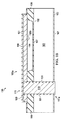
図1Aは、例示の一実施例に従った、単一CUMTセル100aを備えたCUMT要素として示される、例示のCUMTデバイス100を図示する。後述の図1B及び他の図2A〜図2Hに示す断面図のために切断線A−A’が提供されている。CUMTセル100aは、基板貫通ビア(TSV)111、及び頂部側102と底部側103とを有する単結晶材料(例えば、単結晶基板上のバルク単結晶シリコン又はシリコンエピタキシャル層)の第1の基板101を含む。
FIG. 1A illustrates an
図1Bに示すように、頂部側102はその上に、厚い誘電体領域106と薄い誘電体領域107とを含んで、パターニングされた誘電体層を含む。TSV111は、薄膜層120の頂部表面まで第1の基板101の全厚に延在する。TSV111は、誘電体ライナー131により、第1の基板101及び薄膜層120から電気的に絶縁される。誘電体ライナー131は、厚い誘電体領域106の側壁上を含むTSV111の全長に沿って示されているが、熱的に形成される誘電体ライナー131(例えば、シリコン酸化物)の場合は、堆積される誘電体ライナー131とは対照的に、誘電体ライナー131は、厚い誘電体領域106の側壁上に成長せず、そのため厚い誘電体領域106の側壁上にはない。TSV111は、一つの特定の実施例においてCuなど、TSV充填材料113を含む。TSV111はまた、第1の基板101の底部側103から突出する、任意選択の突出するTSVティップ111aを含んで図示される。
As shown in FIG. 1B, the
SOI(silicon on insulator)基板115(図2Aで示す)として示される第2の基板の薄膜層120は、厚い誘電体領域106にボンディングされ、また、図示されるMEMSキャビティ114の上の可動薄膜120bを提供するため第1の基板101の薄い誘電体領域107の上にある。このボンディングは、真空融解ボンディングなどの真空ボンディングを含み得る。パターニングされた頂部側金属層(例えば、AlCu層)161が、TSV111の頂部の上、及び、TSV111を可動薄膜120bに結合する金属層部分を含む可動薄膜120bの頂部の上にある。誘電体パッシベーション層168がCUMTセル100aの頂部の上に示されている。
A
第1の基板101は、単結晶シリコン、又は単結晶シリコン上のエピタキシャルシリコンを含み得る。第1の基板101は典型的に、0.1Ω‐cmより小さいか又はそれに等しい(≦)抵抗を有し、p型又はn型ドープされ得る。CUMTセル100aは、第1の基板101の底部側103のパターニングされた金属層167を含んで示されており、これは、固定電極を実現するためにCUMTセル100aの底部側103の第1の電極コンタクトを提供する。上述のように、CUMTデバイスが、各々複数のCUMTセル100aを含む複数のCUMT要素を含む場合、パターニングされた金属層167により提供される固定電極コンタクトは、CUMTデバイス上の全てのCUMT要素に対する共通底部側固定電極(例えば、Siシートなどの、第1の基板101の固体シート)のためのものである。
The
TSV111は、可動薄膜120bへの底部側接続を提供し、可動薄膜120bは、CUMTデバイス100のCUMTセル100aのための頂部プレートを提供する。上述のように、複数のCUMT要素を有するCUMTデバイスでは、頂部電極は各CUMT要素に対して個別とされ得、各要素のためそれぞれのTSV111を用いるそれぞれの要素の個別アドレス指定を可能にする。そのため、CUMTデバイス100により必要とされる頂部側コンタクト又はボンドパッドはない。
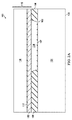
CUMTデバイスの厚み及び寸法は特定の用途に合うように調節され得ることを留意されたい。例えば、180kHzオペレーションでの空中(airborne)超音波用途のための典型的な例示の寸法は、直径が1.12mmの可動薄膜120b、1.32mmのプレート幅のパターニングされた頂部側金属層161(CUMTセル100aの側面上の頂部側金属層161の100μmプレート重なり)、及び14μmの厚みの可動薄膜120bを有するCUMTセルである。
Note that the thickness and dimensions of the CUMT device can be adjusted to suit a particular application. For example, typical exemplary dimensions for airborne ultrasound applications at 180 kHz operation include a movable
図2A〜図2Hは、例示の一実施例に従って、異なる製造段階の間のCUMTデバイスを形成する例示の方法における工程を図示する。説明するCUMTデバイスは単一CUMTセンサセルを備えた単一要素を有して形成されるが、上述のように開示されるCUMTデバイスが、複数のCUMT要素を有するCUMTアレイを形成するように1つ又は複数のCUMTセルを各々が備えた、複数のCUMT要素を有して形成されてもよい(後で説明する図3を参照されたい)。 2A-2H illustrate steps in an exemplary method of forming a CUMT device during different manufacturing stages, according to an exemplary embodiment. The described CUMT device is formed with a single element with a single CUMT sensor cell, but one such that the CUMT devices disclosed as described above form a CUMT array with multiple CUMT elements. Or it may be formed with a plurality of CUMT elements, each comprising a plurality of CUMT cells (see FIG. 3 to be described later).
図2A〜図2Hは、単一CUMTセル100aを備えた単一CUMT要素を有するCUMTデバイスを形成する例示の方法のための処理における工程を図示する。複数の開示されるCUMT要素を含むCUMTデバイスを形成することを含み、開示されるCUMTデバイスを形成するための他の手法を本開示の範囲から逸脱することなく用いることができる。CUMT要素内の幾つかのCUMTセルが、所与のエリアにわたる出力圧力を増大させるためなど、所与のCUMT要素におけるCUMTセルの可動薄膜120bを共に結合することにより並列に接続され得る。CUMTセルを並列に接続することで、(駆動のための)インピーダンスが低減される。CUMT要素は、ビームステアリングを独立的に促進するために用いるため又は大きなエリアにわたる改善された空間的解像度のため、互いに電気的に絶縁され得る。また、コモンモード信号を改善するため又は製造不均整を緩和するために、差動的にCUMT要素を駆動/感知することもできる。
2A-2H illustrate steps in a process for an exemplary method of forming a CUMT device having a single CUMT element with a
シリコン酸化物層を含むなどの厚い誘電体領域106が、第1の基板101の頂部側102に提供される。第1の基板101は、概して、シリコンベースの基板又は他の基板を含む、任意の単結晶基板材料を含み得る。第1の基板101は、約0.01Ω‐cmなど、0.1Ω‐cmに等しいかそれより小さい低基板抵抗を提供する。
A thick
一つの特定の実施例において、厚い誘電体領域106aを形成するため、厚いシリコン酸化物層が、高圧酸化(HiPOx)プロセスを用いて4.5μm〜5.5μmの厚みまで成長される。HiPOxの利用は、厚い熱的酸化物層の急速な成長を促進し、また概して、ダイにわたって典型的に±1%未満の良好な厚み制御を提供する。1つの特定の例示のセットのHiPOxプロセス条件には、最初の(virgin)第1の基板101(例えば、バルク単結晶シリコンウエハ)上で9.5時間の蒸気内の25気圧の1,000℃の温度が含まれ、フォトリソグラフィのための整合マークが後にこのプロセスにおいてエッチングされる。 In one particular embodiment, a thick silicon oxide layer is grown to a thickness of 4.5 μm to 5.5 μm using a high pressure oxidation (HiPOx) process to form a thick dielectric region 106a. Utilizing HiPOx facilitates rapid growth of thick thermal oxide layers and generally provides good thickness control, typically less than ± 1%, across the die. One particular exemplary set of HiPOx process conditions includes a virgin first substrate 101 (eg, a bulk single crystal silicon wafer) at 25 ° C. in a 9.5 hour steam at 1,000 ° C. The alignment marks for photolithography are later etched in this process.
代替として、厚い誘電体領域106はまた、(例えば、概して酸化に対するマスクとしてシリコン窒化物を用いてシリコンウエハ上の選択されたエリア(ここでは厚い誘電体領域106)に二酸化シリコンが形成される、シリコンの局所酸化(LOCOS)プロセスを用いる)従来の熱的成長されたシリコン酸化物を含み得るか、又は、シリコン酸化物又は他の誘電性材料を含む堆積された誘電体層であり得る。しかし、従来の酸化を用いるLOCOSアプローチは概して5μmの厚みの(又は一層厚い)酸化物層を生成せず、堆積される誘電体(例えば、酸化物)フィルムは、概してダイにわたって±1%未満の厚み制御を提供しない。
Alternatively, the thick
最小の表面汚染又は粗さを確実にするために、一般に存在する基板ベンダーのレーザースクライブを用いることができ、これは後続のウエハボンディング工程の助けとなり得る。表側整合マークのマスキング及びエッチングがこれに続き得る。レジストストリップ及び事前洗浄プロセスが、厚い誘電体領域106のための滑らかな表面を確実にすることを助け得、厚い誘電体領域106は、SOI基板115又は標準的なバルクシリコン基板などの第2の基板の、それに対するボンディング薄膜層120のためのプロセスにおいて後に用いられる。
In order to ensure minimal surface contamination or roughness, generally existing substrate vendor laser scribes can be used, which can aid in subsequent wafer bonding steps. This may be followed by masking and etching of the front side registration marks. The resist strip and pre-clean process can help ensure a smooth surface for the thick
第1の基板101(例えば、Siウエハ)上の各CUMTアレイ/ダイに対し少なくとも1つのエッチングされた単一セルCUMT要素を画定することをまず開始するため、第1のマスキングレベル「CELLETCH」が、厚い誘電体領域106(例えば、厚いシリコン酸化物層)を介する後続のエッチングをサポートするために厚いフォトレジストを用いる。厚い誘電体領域106がシリコン酸化物を含み且つ約5μm〜5.3μmの厚みを有するときに約4.65μmのシリコン酸化物をエッチングするためなど、厚い誘電体領域106の第1の部分をエッチングするために、非重合であるプラズマエッチングを用いることができる。80度までの側壁傾斜が概して望ましく、これは自然レジスト浸食から達成され得る。プラズマエッチングの後、厚い誘電体領域106の残りの部分(例えば、0.5μmのシリコン酸化物)は、第1の基板101の頂部側102を損傷させることを避けるために、基板材料(例えば、Si)に対してエッチング選択性を提供するウェットエッチングによって取り除かれ得る。
In order to first begin to define at least one etched single cell CUMT element for each CUMT array / die on the first substrate 101 (eg, Si wafer), a first masking level “CELLETCH” A thick photoresist is used to support subsequent etching through a thick dielectric region 106 (eg, a thick silicon oxide layer). Etch a first portion of thick
第1の基板101(例えば、ウエハ)の頂部側102の約50%が、厚い誘電体領域106のエッチングの間、概して開かれ(露出され)得る。レジストはその後剥がされる(例えば、湿式ストリッププロセス)。適切な事前酸化洗浄に続いて、酸化工程において、薄い誘電体領域107を形成するように、薄い(例えば、0.3μmの)CUMTセル酸化物が成長され得る。
Approximately 50% of the
図2Aは、SOI基板(例えば、SOIウエハ)115の真空融解ボンディング後の製造過程のCUMTデバイスの断面図を示し、SOI基板115は、ハンドル(例えば、ウエハ)116、埋め込み誘電体層117(概して当業界で「埋め込み酸化物層」又は「(BOX)層」と称される)、及び薄膜層120(例えば、概してSOIの分野において「アクティブ層」と称される)を含む。薄膜層120は、第1の基板101の厚い誘電体領域106にボンディングされる。
FIG. 2A shows a cross-sectional view of a CUMT device during manufacturing after vacuum melt bonding of an SOI substrate (eg, SOI wafer) 115, which includes a handle (eg, wafer) 116, a buried dielectric layer 117 (generally And a thin film layer 120 (eg, generally referred to as an “active layer” in the field of SOI), referred to in the art as a “buried oxide layer” or “(BOX) layer”. The
犠牲のハンドル116は、ドープされていない又は軽くドープされた(n又はp型ドープされた)シリコンなどの任意の適切な材料から形成される、任意の適切な半導体ウエハを表し得る。同じく犠牲の埋め込み誘電体層117は、シリコン酸化物層などの電気的に絶縁性の(誘電体)材料の任意の適切な層であり得る。薄膜層120は、ドープされた単一結晶シリコンなどの基板材料の任意の適切な層を表す。特定の実施例において、ハンドル116は、約5〜10Ω‐cmの抵抗のシリコンウエハを含み、埋め込み誘電体層117は、約1.5μm〜2.5μmの厚みであるシリコン酸化物層を表し、薄膜層120は、約5Ω‐cmの抵抗のドープされたシリコンが約14μm±5μmの厚みであることを表す。セル間又は要素間の電気的相互接続の目的のため、薄膜層120は、その上に金属層を含み得、これは、経路に低抵抗経路を提供させる。
しかし、上述のように、コストを低減するためSOI基板の代替として、標準的なシリコンバルク基板材料(例えば、バルクSiウエハ)を含む第2の基板が、第1の基板101(CUMT基板/ウエハ)の厚い誘電体領域106にボンディングされ得る。この実施例において、ボンディング後、第2の基板材料は、14μm±5μmの厚みなど所望のターゲット薄膜厚みまでバックグラインド及び研磨によって薄化され得る。
However, as described above, as an alternative to an SOI substrate to reduce cost, a second substrate comprising a standard silicon bulk substrate material (eg, a bulk Si wafer) is replaced by the first substrate 101 (CUMT substrate / wafer). ) Thick
CUMTデバイス/ダイが複数のCUMT要素(CUMTアレイ)を含む実施例では、薄膜層120は、各CUMT要素における全てのCUMTセルに対し電気的に共通であり得る。各CUMT要素が、要素内のセルに対する複数の電気的に接続される可動薄膜120bを含む個別の/特有の頂部プレートを有し得、これらは、第1の基板101の底部側103からアクセス可能な専用TSVを介して電気的に接続され得る。各CUMT要素の頂部プレートの低抵抗は、可動薄膜120b上の後続の金属堆積によって及びこれ以降に説明するようなパターニング処理工程によって提供され得る。洗浄及びプラズマ事前処理を含む適切な既知のボンディング手法を用いることができる。
In embodiments where the CUMT device / die includes multiple CUMT elements (CUMT arrays), the
真空融解ウエハボンディングでは、当業界で通常既知であるように、良好なウエハボンディングを確実にする属性には、典型的に3A未満の表面粗さの滑らかなボンディング面が含まれる。成長された熱的酸化物及びシリコン基板は概してこの要件を満たす。ボンディング前に、表面は、典型的に10分間、75又は80℃でNH4OH(水酸化アンモニウム)+H2O2(過酸化水素)+H2O(水)の1:1:5溶液で、RCA洗浄(SC−1、ここで、SCは標準的な洗浄(Standard Clean)を表す)で処理され得る。第2のRCA洗浄工程は、薄い酸化物層及びいくらかのイオン性汚染物質を取り除くために、25℃のHF+H2Oの1:50溶液における短時間浸漬である。第3及び最後の工程のRCA洗浄(SC−2と称される)は、75又は80℃のHCl+H2O2+H2Oの1:1:6溶液で実施される。この処理は、金属性(イオン性)汚染物質の残ったトレースを効率的に取り除く。N2プラズマアクティベーション及びDI水リンスがこれに続き得る。真空ボンディングは典型的に、8×10⁵mbar未満の圧力で実施される。最終的な工程として、ボンディングされた表面は、4時間の1050℃N2アニールなど、数時間N2内でアニーリングされる。 In vacuum melting wafer bonding, as is commonly known in the art, attributes that ensure good wafer bonding typically include a smooth bonding surface with a surface roughness of less than 3A. Grown thermal oxide and silicon substrates generally meet this requirement. Prior to bonding, the surface is typically a 1: 1: 5 solution of NH 4 OH (ammonium hydroxide) + H 2 O 2 (hydrogen peroxide) + H 2 O (water) at 75 or 80 ° C. for 10 minutes, It can be treated with RCA cleaning (SC-1, where SC stands for Standard Clean). The second RCA cleaning step is a brief immersion in a 1:50 solution of HF + H 2 O at 25 ° C. to remove the thin oxide layer and some ionic contaminants. The third and last step RCA wash (referred to as SC-2) is performed with a 1: 1: 6 solution of HCl + H 2 O 2 + H 2 O at 75 or 80 ° C. This treatment effectively removes the remaining traces of metallic (ionic) contaminants. This can be followed by N 2 plasma activation and DI water rinse. Vacuum bonding is typically performed at a pressure of less than 8 × 10 5 mbar. As a final step, the bonded surfaces are annealed in N 2 for several hours, such as a 4 hour 1050 ° C. N 2 anneal.
ハンドル116はその後、約150μmのポストバックグラインドターゲットまでハンドル116をバックグラインドすること、バックグラインド後、バックグラインド後に残ったハンドルのウェットエッチング前に、第2の4時間1050℃アニールを実施すること、及びその後、残ったハンドルをウェットエッチングすることによるなど、ボンディング後に取り除かれる。ハンドル116がシリコンを含むとき、バックグラインド後に残ったハンドルは、水酸化物(例えば、KOH又はTMAH)を用いるなど、埋め込み誘電体層117で止まる、ウェットシリコンエッチングにおいてエッチングされ得る。可動薄膜(例えば、シリコンプレート)120bをマスキング及びエッチングすることで、整合マークを再び開けるため及び後続の処理工程のための適切な整合を可能にするために、整合マークの上の薄膜層120が取り除かれる。薄膜層120はエッチングのため概して比較的厚い層である(例えば、約14μmの厚み)ため、Boschエッチングが、薄膜層120のエッチングの間、レジスト浸食を補償し得る。当業界で既知であるように、パルスされた又は時間多重化されたエッチングとしても知られているBoschプロセスは、ほぼ垂直のエッチングされた構造を得るために2つのモード/位相間で反復的に交替する。
The
図2Bは、マスキングレベルMask「TSVHOLE」(マスク#2)後の製造過程のCUMTデバイスを図示する。一つの特定の実施例において、TSVホール(埋め込みビア)219は、直径が30μmで150μmの深さ(総深さ)である。レジスト217は、1.1μmの埋め込み誘電体層117、及び14μmの薄膜層120、及び5.1μmの厚い誘電体領域106、及び第1の基板101内に130μmなど、提供されるスタックを介するエッチングをサポートするために充分な厚みであるべきである。その後、TSVホール219はエッチングされる。埋め込み誘電体層117(例えばシリコン酸化物)をエッチングするため及びシリコンの場合に第1の基板101をエッチングするためのBoschエッチングに、個別のエッチングツールを用いることができる。
FIG. 2B illustrates the in-process CUMT device after masking level Mask “TSVHOLD” (mask # 2). In one particular embodiment, the TSV hole (buried via) 219 is 30 μm in diameter and 150 μm deep (total depth). Resist 217 is etched through a provided stack, such as a 1.1 μm buried
その後、レジスト217は剥がされ、誘電体ライナー131(例えば、0.5μmの誘電体酸化物)が、埋め込みビア/TSVホール219内の半導体表面上に堆積されるか又は熱成長される。誘電体ライナー131上に形成される拡散障壁金属層が、TSVをフレーミングし、Cuなどの高度に可動性の金属TSV充填材料の場合に半導体へのTSV充填材(又はコア)材料113の流出(escape)から保護する。例えば、一つの特定の実施例において、0.0875μmのTa/TaN拡散障壁金属層及び1.5μmのCuシード層233(図2C参照)が、銅TSV充填材料113の実施例のために誘電体ライナー131上に堆積される。代替として、シード層233は、例えば、チタンの上の銅を含み得る。
Thereafter, the resist 217 is stripped and a dielectric liner 131 (eg, 0.5 μm dielectric oxide) is deposited or thermally grown on the semiconductor surface in the buried via /
図2Cは、レジスト221を用いるマスキングレベルMask「CUMOLD」(マスク#3)後の製造過程のCUMTデバイスを図示する。このマスクは、CUMTセルの一部の上のめっきからCuなどの金属を排除するために用いられ得る。マスキング後TSVにレジストがないことを確実にするためにネガティブレジストが用いられ得る。可動薄膜120b(例えば、Siプレート)が数ミクロン撓み得、また、銅充填されたTSVの場合の後続のCu化学機械研磨(CMP)工程がCUMTセルの上の銅を完全には取り除かない可能性があるため、このマスクは有効である。
FIG. 2C illustrates the in-process CUMT device after masking level Mask “CUMOD” (mask # 3) using resist 221. This mask can be used to exclude metals such as Cu from plating on a portion of the CUMT cell. A negative resist can be used to ensure that there is no resist in the TSV after masking. Movable
その後、充填されたTSVホール219をTSV充填材料113で画定するための後続のCMPで(例えば、約15μmのCuが用いられる)、TSV充填材料113を電気めっきすることなどで、金属層が堆積される。レジスト221はその後剥がされる。図2Dは、埋め込みTSV111’の上の及びその横のシード層233上のTSV充填材料113から金属ネールヘッドが取り除かれて示されるような、TSV充填材料113のCMP、及びフィールドエリアの上の埋め込み誘電体層117と共に誘電体ライナー131が除去された後の、TSV充填材料113堆積(例えば、Cu)後の製造過程のCUMTデバイスの断面図を示す。アニール工程がこれに続き得る。存在する場合に全ての残りの障壁金属(例えばCu+TaN)を取り除くために、第2のTSV CMPが用いられ得る。CUMTセルの上の残留物を取り除くためにウェットストリップが用いられ得る。その後、誘電体ライナー131は埋め込み誘電体層117と共に取り除かれ、薄膜層120(例えば、Si)上で止まる。
A metal layer is then deposited, such as by electroplating the
図2Eは、0.5μmの厚みのAlCu金属層など、頂部側金属層161の堆積後の製造過程のCUMTデバイスを図示する。頂部側金属層161は、薄膜層120プレートメタライゼーションを提供し、薄膜層120を埋め込みTSV111’の頂部側に接続する。レジスト223を用いるマスキングレベル「ALTOP」(マスク#4)が示されており、これにより、CUMT要素の上の頂部側金属層161(例えば、AlCu層)を画定するためのエッチングが可能となる。ALTOP CDは、最終的なプレート寸法より小さく(例えば、1μm/辺小さく)され得る。可動薄膜120(例えば、Siプレート)をパターニングする前に頂部側金属層161をパターニングすることで、頂部側金属層161及びレジストステップカバレッジ問題両方が避けられる。頂部側金属層161は、レジスト223における開口を用いてフィールドエリアからウェットエッチングされ得る。レジスト223はその後剥がされる。
FIG. 2E illustrates a manufacturing CUMT device after deposition of a
図2Fは、マスクレベル「PLATESI」(マスク#5)を用いるレジスト225のパターニング後の製造過程のCUMTデバイスを図示する。レジスト225は、パターニングされた頂部側金属層161(例えば、AlCu層)を完全に封止し得る。このマスクは、上述のAlCu(ALTOP)マスクより大きく(例えば、1μm/辺大きく)され得る。 FIG. 2F illustrates a manufacturing CUMT device after patterning of resist 225 using mask level “PLATESI” (mask # 5). The resist 225 may completely seal the patterned top metal layer 161 (eg, AlCu layer). This mask can be larger (eg, 1 μm / side larger) than the AlCu (ALTOP) mask described above.
その後、薄膜層120は、複数のCUMT要素を有するCUMTデバイスのためにCUMT要素を分けるため、及び図示される可動薄膜120bを形成するために、レジスト225を用いてエッチングされる。薄膜層120のエッチングは、厚い誘電体領域106上で止まる。側壁スカロップ(scalloping)を最小化するために、短いサイクルのBoschエッチングが用いられ得る。このエッチングは、凹まないように構成されるべきである。レジスト225はその後剥がされ得る。
The
図2Gは、一つの特定の実施例において、約0.2μmのプラズマオルトケイ酸テトラエチル(TEOS)由来のシリコン酸化物層、及びその後の、0.2μmのプラズマ窒化物パッシベーション層など、誘電体パッシベーション層168を堆積した後の製造過程のCUMTデバイスを図示する。誘電体パッシベーション層168は、可動薄膜120bの側壁を覆って示されている。CUMT用途に応じて、一層厚いパッシベーションスタックを用いることができる。最終的な合金が、N2+H2(形成ガス)内の400℃などで実施され得る。
FIG. 2G illustrates a dielectric passivation layer, such as a silicon oxide layer from about 0.2 μm plasma orthosilicate (TEOS), followed by a 0.2 μm plasma nitride passivation layer in one particular embodiment. FIG. 4 illustrates a CUMT device in manufacturing after deposition of 168. FIG. A
図2Hは、任意選択で、接着剤172を用いて一時キャリアウエハ180に製造過程CUMT基板(例えば、ウエハ)をボンディングし、第1の基板101の底部側103のTSVをバックグラインドして露出させ、突出するTSVティップ111aを形成した後の、製造過程のCUMTデバイスを図示する。バックグラインドは、埋め込みTSV近くの製造過程CUMT基板(例えば、ウエハ)を薄化し得、また、全ての底部側フィルムを取り除き得、一つの特定の実施例において、第1の基板101のための725μmの厚みのSi基板のうちの約550μmを取り除き、約175μmを残す。第1の基板101の底部側103は、約100μmの厚みとなるように第1の基板101を残して、TSVティップ111aを露出するようにエッチングされ得る。TSV111のための露出されたTSV充填材料113を有するTSVティップ111aを形成するために誘電体ライナー131及び障壁金属(存在する場合)が取り除かれるように、XeFプラズマエッチング又はウェットSiエッチングを用いることができる。誘電体ライナー131及び障壁金属のプラズマエッチングが、TSV111及び112の側壁上に誘電体(例えば、酸化物)スペーサを概して残す。
FIG. 2H optionally bonds a manufacturing process CUMT substrate (eg, a wafer) to the
その後、1つの特定の実施例においてTi/Ni/Ag層(例えば、1000ÅのTi+2800ÅのNi+1500ÅのAg)など、第1の基板の底部側103上に金属層が堆積される。第1の基板101の底部側103は、金属層167堆積前に洗浄され得る。約300Åの事前スパッタエッチングが用いられ得る。その後、マスキングレベル「TSVEXP」(マスク#6)が、金属層167のエリアを保護するために用いられ得、一方、それはTSVティップ111aから剥がされる。第1の基板101の底部側103のパターニングされた金属層167を形成するためのパターニング、及びマスク6レジストのストリップの後、上述で図1Bに示すCUMTデバイス100が生じる(図1BにはCuシード層233が示されていない)。ダイシング(シンギュレーション)に続いて、結果のCUMTダイは、制御ダイの頂部上にボンディングされるなど、パッケージングされ得る。
Thereafter, a metal layer is deposited on the
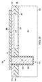
図3は、複数のCUMT要素301〜306を含む、例示のCUMTデバイス(ダイ)300を示す。例示の一実施例に従って、各容量性CUMT要素は、要素内で共に接続されるCUMTセル100a〜100dとして示される4つの図1A及び図1BにおけるCUMTセル100aを含む。上述のように、頂部電極は、各CUMT要素に対して個別であり得、そのため、各要素に対して単一TSVを用いるそれぞれの要素の個別アドレス指定が可能となり、この場合、デバイス上の全てのCUMT要素のための共通底部側電極(例えば、Siの固体シート)がある。他の実施例において、CUMTデバイスは、各要素のための共通頂部電極、及びそれぞれの要素の個別のアドレス指定を可能にするための各要素のための個別の底部電極を有する。
FIG. 3 shows an exemplary CUMT device (die) 300 that includes a plurality of CUMT elements 301-306. In accordance with one exemplary embodiment, each capacitive CUMT element includes four
各CUMT要素が4つのCUMTセル100a〜100dを含む、6つのCUMT要素301〜306を有するCUMTデバイス300が示されているが、開示されるCUMTデバイスは、各々が任意の数のCUMTセルを有する任意の数のCUMT要素を有していてよい。CUMT要素301〜306は、互いに電気的に絶縁され得、(駆動のため)インピーダンスを低減するために(例えば、それらのそれぞれのTSV111を共通ソースに接続することにより)ダイに接して又はダイから離れて並列に接続され得、又は(感知のため)インピーダンスを増大させるために(ダイに接して又はダイから離れて)直列に接続され得る。それぞれのCUMT要素は、コモンモード信号を差動的に改善するため又は製造不均整を緩和するために駆動/感知され得る。
Although a
開示されるCUMTデバイスの利点には、4程度に少ないマスクレベルを用いるフルプロセスが含まれる。他の利点には、CUMTデバイスの頂部側の超音波伝送表面(可動薄膜120b)に結合するためにダイサイズを増大させ且つワイヤボンディングを必要とする従来のボンドパッドを必要とすることなく、一層小さなダイサイズが可能となることが含まれる。開示されるCUMTデバイスはまた、パッケージングオペレーションを単純化し、その結果、伝送媒体への結合が容易となり、これによりパッケージングコストが低減される。両電極がCUMTデバイスの底部側から接触されるため、開示されるCUMTデバイスはまた、制御ダイ上にCUMTダイをスタックするオプションを促進する。
Advantages of the disclosed CUMT device include a full process using as few as 4 mask levels. Another advantage is that it does not require a conventional bond pad that increases the die size and requires wire bonding to bond to the ultrasonic transmission surface (movable
開示される実施例は、種々の異なるデバイス及び関連する製品を形成するために種々のアッセンブリフローに統合され得る半導体ダイを形成するために用いることができる。当業者であれば、本発明の特許請求の範囲内で、説明した例示の実施例に変形が成され得ること、及び多くの他の実施例が可能であることが分かるであろう。 The disclosed embodiments can be used to form semiconductor dies that can be integrated into various assembly flows to form a variety of different devices and related products. Those skilled in the art will appreciate that variations can be made to the described exemplary embodiments and that many other embodiments are possible within the scope of the claims of the present invention.
Claims (20)
前記CMUTセルが、
頂部側と底部側とを含む基板と、
前記基板の頂部側の上の誘電体層であって、第1の領域と、前記第1の領域により横方向に囲まれて前記第1の領域よりも薄い第2の領域とを含み、前記第1及び第2の領域がキャビティを定める、前記誘電体層と、
前記誘電体層の第1の領域上に直接に接合され、前記誘電体層の第2の領域の上で前記キャビティを取り囲む薄膜層であって、前記キャビティ内に可動薄膜を含む、前記薄膜層と、
前記基板と前記誘電体層と前記薄膜層とに入り込み、前記可動薄膜から横方向に離れて位置する基板貫通ビア(TSV)であって、前記薄膜層と共面になるように、前記基板の底部側から延在する導電性充填材を含む、前記基板貫通ビア(TSV)と、
前記基板の頂部側の上で前記導電性充填材に接する金属層であって、前記薄膜層に沿って横方向に延び、前記可動薄膜に接する、前記金属層と、
を含む、デバイス。 A CMUT device comprising a capacitive micromachined ultrasonic transducer (CM U T) cell comprising :
The CM U T cell is
A substrate including a top side and a bottom side;
A dielectric layer on the top side of the substrate, seen including a first region, and said first thinner than the surrounded laterally first region by region the second region, It said first and second regions define a cavity, and the dielectric layer,
Said dielectric layer being first directly bonded to a region of the a dielectric layer second film layer surrounding the cavity over a region of the includes a movable film in the cavity, the thin film layer And
A through-substrate via (TSV) that penetrates the substrate, the dielectric layer, and the thin film layer and is laterally separated from the movable thin film, and is coplanar with the thin film layer . containing a conductive filler which extends from the bottom side, and the substrate through via (TSV),
A metal layer in contact with the conductive filler on the top side of the substrate, extending laterally along the thin film layer, in contact with said movable membrane, and the metal layer,
Including the device.
前記金属層の上の誘電性パッシベーション層を更に含む、デバイス。 The CMUT device according to claim 1,
The device further comprising a dielectric passivation layer over the metal layer.
第2のCMUTセルと、
前記基板の底部側の下の前記第1のCMUTセルの前記導電性充填材に接して前記第1のCMUTセルを前記第2のCMUTセルに接続する第2の金属層と、
を更に含む、デバイス。 The CMUT device according to claim 1,
A second CMUT cell;
A second metal layer that connects the first CM U T cell in contact with said conductive filler of said first CM U T cell below the bottom side of the substrate to the second CM U T cells When,
Further comprising a device.
前記薄膜層が単結晶シリコン材料を含む、デバイス。 The CMUT device according to claim 1,
The device, wherein the thin film layer comprises a single crystal silicon material .
前記導電性充填材が、銅を含み、前記基板の前記底部側から突出する、デバイス。 The CMUT device according to claim 1,
It said conductive filler comprises copper, protruding from the bottom side of the substrate, the device.
前記基板が、0.1Ω−cmより小さいか又はそれに等しい抵抗を有する、デバイス。 The CMUT device according to claim 1,
The device, wherein the substrate has a resistance less than or equal to 0.1 Ω-cm.
前記薄膜層が前記誘電体層に真空融解ボンディングされる、デバイス。 The CMUT device according to claim 1,
The device, wherein the thin film layer is vacuum melt bonded to the dielectric layer .
第1の側と第1の側の反対の第2の側とを有する基板と、A substrate having a first side and a second side opposite the first side;
トランスデューサセルと、A transducer cell;
を含み、Including
前記トランスデューサセルが、The transducer cell comprises:
前記基板の第1の側の上の誘電体層であって、第1の領域と、第1の領域よりも薄く、キャビティを定めるために前記第1の領域により横方向に囲まれる第2の領域とを有する、前記誘電体層と、A dielectric layer on a first side of the substrate, the first layer being thinner than the first region and laterally surrounded by the first region to define a cavity; The dielectric layer having a region;
前記キャビティを取り囲み、前記誘電体層の第2の領域の上に可動薄膜を含む薄膜層と、A thin film layer surrounding the cavity and including a movable thin film over a second region of the dielectric layer;
前記基板と前記誘電体層と前記薄膜層とに入り込む貫通基板ビア(TSV)と、A through-substrate via (TSV) that enters the substrate, the dielectric layer, and the thin film layer;
を含む、デバイス。Including the device.
前記薄膜層が前記誘電体層の第1の領域上に直接に接合される、デバイス。The device, wherein the thin film layer is bonded directly onto the first region of the dielectric layer.
前記TSVが、前記可動薄膜に垂直に重なっていない、デバイス。The device, wherein the TSV does not overlap the movable thin film perpendicularly.
前記TSVが、前記薄膜層と共面になるように前記基板の第2の側から延びる導電性充填材を含む、デバイス。The device, wherein the TSV includes a conductive filler that extends from a second side of the substrate to be coplanar with the thin film layer.
前記基板の第1の側に隣接する前記TSVに接する金属層であって、前記薄膜層に沿って横方向に延び、前記可動薄膜に接する、前記金属層を更に含む、デバイス。A device further comprising a metal layer in contact with the TSV adjacent to the first side of the substrate, the metal layer extending laterally along the thin film layer and in contact with the movable thin film.
前記薄膜層が単結晶シリコン材料を含む、デバイス。The device, wherein the thin film layer comprises a single crystal silicon material.
第2のトランスデューサセルと、A second transducer cell;
前記第2のトランスデューサセルを前記基板の第2の側に隣接する前記トランスデューサセルの前記TSVに接続する金属層と、A metal layer connecting the second transducer cell to the TSV of the transducer cell adjacent to the second side of the substrate;
を更に含む、デバイス。Further comprising a device.
第1の側と前記第1の側の反対の第2の側とを有する基板と、A substrate having a first side and a second side opposite the first side;
複数のトランスデューサセルであって、各トランスデューサセルが、A plurality of transducer cells, each transducer cell comprising:
前記基板の第1の側の上の誘電体層であって、第1の領域と、前記第1の領域よりも薄く、キャビティを定めるように前記第1の領域により横方向に囲まれる第2の領域とを有する、前記誘電体層と、A dielectric layer on a first side of the substrate, the first region and a second region that is thinner than the first region and laterally surrounded by the first region to define a cavity; The dielectric layer having a region of
前記キャビティを取り囲む薄膜層であって、前記誘電体層の第2の領域の上に可動薄膜を含む、前記薄膜層と、A thin film layer surrounding the cavity, the thin film layer comprising a movable thin film over a second region of the dielectric layer;
前記基板と前記誘電体層と前記薄膜層とに入り込む貫通基板ビア(TSV)であって、誘電体充填材を含む、前記TSVと、A through-substrate via (TSV) that enters the substrate, the dielectric layer, and the thin film layer, the TSV comprising a dielectric filler;
を含む、前記複数のトランスデューサセルと、A plurality of transducer cells comprising:
前記基板の第2の側に隣接する少なくとも2つの前記トランスデューサセルの導電性充填材に接続する相互接続金属層と、An interconnect metal layer connected to conductive fillers of at least two of said transducer cells adjacent to a second side of said substrate;
を含む、デバイス。Including the device.
前記薄膜層が前記誘電体層の第1の領域に直接に接合される、デバイス。The device, wherein the thin film layer is bonded directly to the first region of the dielectric layer.
前記TSVが、前記可動薄膜に垂直に重ならない、デバイス。The device, wherein the TSV does not overlap vertically with the movable thin film.
前記導電性充填材が、前記薄膜層と共面となるように前記基板の第2の側から延びる、デバイス。The device, wherein the conductive filler extends from a second side of the substrate so as to be coplanar with the thin film layer.
前記基板の第1の側に隣接する前記TSVに接する相互セル金属層であって、前記薄膜層に沿って横方向に延び、前記可動薄膜に接する、前記相互セル金属層を更に含む、デバイス。A device further comprising a mutual cell metal layer in contact with the TSV adjacent to the first side of the substrate, extending laterally along the thin film layer and in contact with the movable thin film.
前記薄膜層が単結晶シリコン材料を含む、デバイス。The device, wherein the thin film layer comprises a single crystal silicon material.
Applications Claiming Priority (3)
| Application Number | Priority Date | Filing Date | Title |
|---|---|---|---|
| US13/779,376 | 2013-02-27 | ||
| US13/779,376 US9520811B2 (en) | 2013-02-27 | 2013-02-27 | Capacitive micromachined ultrasonic transducer (CMUT) device with through-substrate via (TSV) |
| PCT/US2014/019011 WO2014134301A1 (en) | 2013-02-27 | 2014-02-27 | Capacitive micromachined ultrasonic transducer (cmut) device with through-substrate via (tsv) |
Publications (3)
| Publication Number | Publication Date |
|---|---|
| JP2016511607A JP2016511607A (en) | 2016-04-14 |
| JP2016511607A5 JP2016511607A5 (en) | 2017-04-06 |
| JP6337026B2 true JP6337026B2 (en) | 2018-06-06 |
Family
ID=51387424
Family Applications (1)
| Application Number | Title | Priority Date | Filing Date |
|---|---|---|---|
| JP2015560307A Active JP6337026B2 (en) | 2013-02-27 | 2014-02-27 | Capacitive micromachined ultrasonic transducer (CUMT) device with through-substrate vias (TSV) |
Country Status (4)
| Country | Link |
|---|---|
| US (2) | US9520811B2 (en) |
| JP (1) | JP6337026B2 (en) |
| CN (1) | CN105025802B (en) |
| WO (1) | WO2014134301A1 (en) |
Families Citing this family (16)
| Publication number | Priority date | Publication date | Assignee | Title |
|---|---|---|---|---|
| US9351081B2 (en) | 2013-02-27 | 2016-05-24 | Texas Instruments Incorporated | Capacitive micromachined ultrasonic transducer (CMUT) with through-substrate via (TSV) substrate plug |
| US9520811B2 (en) * | 2013-02-27 | 2016-12-13 | Texas Instruments Incorporated | Capacitive micromachined ultrasonic transducer (CMUT) device with through-substrate via (TSV) |
| US9470710B2 (en) | 2013-02-27 | 2016-10-18 | Texas Instruments Incorporated | Capacitive MEMS sensor devices |
| JP6221582B2 (en) * | 2013-09-30 | 2017-11-01 | セイコーエプソン株式会社 | Ultrasonic device and probe, electronic apparatus and ultrasonic imaging apparatus |
| US9761509B2 (en) * | 2015-12-29 | 2017-09-12 | United Microelectronics Corp. | Semiconductor device with throgh-substrate via and method for fabrication the semiconductor device |
| CA3052485A1 (en) * | 2017-02-27 | 2018-08-30 | Butterfly Network, Inc. | Capacitive micromachined ultrasonic transducers (cmuts) and related apparatus and methods |
| US10662055B2 (en) | 2017-04-27 | 2020-05-26 | Seiko Epson Corporation | MEMS element, sealing structure, electronic device, electronic apparatus, and vehicle |
| KR102450580B1 (en) | 2017-12-22 | 2022-10-07 | 삼성전자주식회사 | Semiconductor Device having a Structure for Insulating Layer under Metal Line |
| CN112004611A (en) * | 2018-03-09 | 2020-11-27 | 蝴蝶网络有限公司 | Ultrasound transducer device and method for producing an ultrasound transducer device |
| JP2022509066A (en) * | 2018-11-16 | 2022-01-20 | ヴァーモン エス.エー. | Capacitive microfabrication ultrasonic transducer and its manufacturing method |
| KR102244601B1 (en) * | 2019-05-29 | 2021-04-26 | 인하대학교 산학협력단 | Capacitive Micromachined Ultrasonic Transducer and method of fabricating the same |
| WO2021038300A1 (en) * | 2019-08-30 | 2021-03-04 | Vermon Sa | Cmut transducer |
| CA3164543A1 (en) * | 2020-01-17 | 2021-07-22 | The University Of British Columbia | Flexible capacitive micromachined ultrasonic transducer arrays |
| US11440051B2 (en) | 2020-02-26 | 2022-09-13 | General Electric Company | Capacitive micromachined ultrasonic transducer (CMUT) devices and methods of manufacturing |
| CN111889341B (en) * | 2020-07-30 | 2021-07-13 | 中国兵器工业集团第二一四研究所苏州研发中心 | Ultrathin flexible silicon-based capacitive micro-machined ultrasonic transducer and processing method |
| EP4059440A1 (en) | 2021-03-15 | 2022-09-21 | Pulsify Medical | Ultrasound system |
Family Cites Families (25)
| Publication number | Priority date | Publication date | Assignee | Title |
|---|---|---|---|---|
| US6312581B1 (en) | 1999-11-30 | 2001-11-06 | Agere Systems Optoelectronics Guardian Corp. | Process for fabricating an optical device |
| TWI221343B (en) | 2003-10-21 | 2004-09-21 | Advanced Semiconductor Eng | Wafer structure for preventing contamination of bond pads during SMT process and process for the same |
| WO2007036922A1 (en) | 2005-09-30 | 2007-04-05 | Timothy Cummins | An integrated electronic sensor |
| JP4347885B2 (en) * | 2004-06-03 | 2009-10-21 | オリンパス株式会社 | Manufacturing method of capacitive ultrasonic transducer, ultrasonic endoscope apparatus including capacitive ultrasonic transducer manufactured by the manufacturing method, capacitive ultrasonic probe, and capacitive ultrasonic transducer Sonic transducer |
| JP4575372B2 (en) * | 2004-06-10 | 2010-11-04 | オリンパス株式会社 | Capacitive ultrasonic probe device |
| US7405637B1 (en) * | 2004-06-29 | 2008-07-29 | Hrl Laboratories, Llc | Miniature tunable filter having an electrostatically adjustable membrane |
| WO2006046471A1 (en) * | 2004-10-27 | 2006-05-04 | Olympus Corporation | Capacitive micromachined ultrasonic transducer and intracorporeal ultrasound diagnostic system using same |
| JP2008541473A (en) * | 2005-05-18 | 2008-11-20 | コロ テクノロジーズ インコーポレイテッド | Through-wafer interconnection |
| CA2607916A1 (en) * | 2005-05-18 | 2006-11-23 | Kolo Technologies, Inc. | Micro-electro-mechanical transducers |
| DE102005058977A1 (en) | 2005-12-09 | 2007-06-14 | Atmel Germany Gmbh | Transponder device with mega-pads |
| US7741686B2 (en) * | 2006-07-20 | 2010-06-22 | The Board Of Trustees Of The Leland Stanford Junior University | Trench isolated capacitive micromachined ultrasonic transducer arrays with a supporting frame |
| JP4891182B2 (en) * | 2007-08-28 | 2012-03-07 | オリンパスメディカルシステムズ株式会社 | Ultrasonic transducer, ultrasonic diagnostic apparatus and ultrasonic microscope |
| US7843022B2 (en) * | 2007-10-18 | 2010-11-30 | The Board Of Trustees Of The Leland Stanford Junior University | High-temperature electrostatic transducers and fabrication method |
| US7799678B2 (en) * | 2008-01-30 | 2010-09-21 | Freescale Semiconductor, Inc. | Method for forming a through silicon via layout |
| US7943514B2 (en) * | 2009-09-03 | 2011-05-17 | Texas Instruments Incorporated | Integrated circuits having TSVs including metal gettering dielectric liners |
| US8143704B2 (en) * | 2009-10-02 | 2012-03-27 | Texas Instruments Incorporated | Electronic assemblies including mechanically secured protruding bonding conductor joints |
| US8563345B2 (en) * | 2009-10-02 | 2013-10-22 | National Semiconductor Corporated | Integration of structurally-stable isolated capacitive micromachined ultrasonic transducer (CMUT) array cells and array elements |
| US8324006B1 (en) * | 2009-10-28 | 2012-12-04 | National Semiconductor Corporation | Method of forming a capacitive micromachined ultrasonic transducer (CMUT) |
| US7969013B2 (en) * | 2009-10-22 | 2011-06-28 | Taiwan Semiconductor Manufacturing Company, Ltd. | Through silicon via with dummy structure and method for forming the same |
| JP5404335B2 (en) * | 2009-11-17 | 2014-01-29 | キヤノン株式会社 | Electromechanical transducer and method for manufacturing the same |
| DE102010045649A1 (en) | 2010-09-17 | 2012-03-22 | Texas Instruments Deutschland Gmbh | Electronic device and method for directly mounting passive components |
| US20140187957A1 (en) * | 2012-12-31 | 2014-07-03 | Volcano Corporation | Ultrasonic Transducer Electrode Assembly |
| US9351081B2 (en) * | 2013-02-27 | 2016-05-24 | Texas Instruments Incorporated | Capacitive micromachined ultrasonic transducer (CMUT) with through-substrate via (TSV) substrate plug |
| US9520811B2 (en) * | 2013-02-27 | 2016-12-13 | Texas Instruments Incorporated | Capacitive micromachined ultrasonic transducer (CMUT) device with through-substrate via (TSV) |
| KR102176584B1 (en) * | 2013-11-20 | 2020-11-09 | 삼성전자주식회사 | Capacitive micromachined ultrasonic transducer and method of fabricating the same |
-
2013
- 2013-02-27 US US13/779,376 patent/US9520811B2/en active Active
-
2014
- 2014-02-27 WO PCT/US2014/019011 patent/WO2014134301A1/en active Application Filing
- 2014-02-27 CN CN201480010856.5A patent/CN105025802B/en active Active
- 2014-02-27 JP JP2015560307A patent/JP6337026B2/en active Active
-
2016
- 2016-11-08 US US15/345,741 patent/US10335827B2/en active Active
Also Published As
| Publication number | Publication date |
|---|---|
| JP2016511607A (en) | 2016-04-14 |
| CN105025802B (en) | 2018-01-05 |
| CN105025802A (en) | 2015-11-04 |
| US20140239769A1 (en) | 2014-08-28 |
| US10335827B2 (en) | 2019-07-02 |
| US20170050217A1 (en) | 2017-02-23 |
| WO2014134301A1 (en) | 2014-09-04 |
| US9520811B2 (en) | 2016-12-13 |
Similar Documents
| Publication | Publication Date | Title |
|---|---|---|
| JP6337026B2 (en) | Capacitive micromachined ultrasonic transducer (CUMT) device with through-substrate vias (TSV) | |
| US9937528B2 (en) | Capacitive micromachined ultrasonic transducer (CMUT) forming | |
| US10967400B2 (en) | Microfabricated ultrasonic transducer having individual cells with electrically isolated electrode sections | |
| US10107830B2 (en) | Method of forming capacitive MEMS sensor devices | |
| US8563345B2 (en) | Integration of structurally-stable isolated capacitive micromachined ultrasonic transducer (CMUT) array cells and array elements | |
| US10093534B2 (en) | Capacitive micromachined ultrasonic transducer and method of fabricating the same | |
| US8222065B1 (en) | Method and system for forming a capacitive micromachined ultrasonic transducer | |
| US9596528B2 (en) | Capacitive micromachined ultrasonic transducer and method of fabricating the same | |
| JP2012519958A (en) | Monolithic integrated CMUT fabricated by low temperature wafer bonding | |
| CN104160721A (en) | High frequency cmut |
Legal Events
| Date | Code | Title | Description |
|---|---|---|---|
| A521 | Request for written amendment filed |
Free format text: JAPANESE INTERMEDIATE CODE: A523 Effective date: 20170227 |
|
| A621 | Written request for application examination |
Free format text: JAPANESE INTERMEDIATE CODE: A621 Effective date: 20170227 |
|
| A131 | Notification of reasons for refusal |
Free format text: JAPANESE INTERMEDIATE CODE: A131 Effective date: 20180404 |
|
| A521 | Request for written amendment filed |
Free format text: JAPANESE INTERMEDIATE CODE: A523 Effective date: 20180404 |
|
| TRDD | Decision of grant or rejection written | ||
| A01 | Written decision to grant a patent or to grant a registration (utility model) |
Free format text: JAPANESE INTERMEDIATE CODE: A01 Effective date: 20180418 |
|
| A61 | First payment of annual fees (during grant procedure) |
Free format text: JAPANESE INTERMEDIATE CODE: A61 Effective date: 20180507 |
|
| R150 | Certificate of patent or registration of utility model |
Ref document number: 6337026 Country of ref document: JP Free format text: JAPANESE INTERMEDIATE CODE: R150 |
|
| S111 | Request for change of ownership or part of ownership |
Free format text: JAPANESE INTERMEDIATE CODE: R313117 |
|
| S533 | Written request for registration of change of name |
Free format text: JAPANESE INTERMEDIATE CODE: R313533 |
|
| R350 | Written notification of registration of transfer |
Free format text: JAPANESE INTERMEDIATE CODE: R350 |
|
| R360 | Written notification for declining of transfer of rights |
Free format text: JAPANESE INTERMEDIATE CODE: R360 |
|
| R250 | Receipt of annual fees |
Free format text: JAPANESE INTERMEDIATE CODE: R250 |
|
| R350 | Written notification of registration of transfer |
Free format text: JAPANESE INTERMEDIATE CODE: R350 |
|
| R250 | Receipt of annual fees |
Free format text: JAPANESE INTERMEDIATE CODE: R250 |
|
| R250 | Receipt of annual fees |
Free format text: JAPANESE INTERMEDIATE CODE: R250 |