JP6315967B2 - Optical scanning device and image forming apparatus using the same - Google Patents
Optical scanning device and image forming apparatus using the same Download PDFInfo
- Publication number
- JP6315967B2 JP6315967B2 JP2013256443A JP2013256443A JP6315967B2 JP 6315967 B2 JP6315967 B2 JP 6315967B2 JP 2013256443 A JP2013256443 A JP 2013256443A JP 2013256443 A JP2013256443 A JP 2013256443A JP 6315967 B2 JP6315967 B2 JP 6315967B2
- Authority
- JP
- Japan
- Prior art keywords
- laser
- drive
- light source
- light sources
- light
- Prior art date
- Legal status (The legal status is an assumption and is not a legal conclusion. Google has not performed a legal analysis and makes no representation as to the accuracy of the status listed.)
- Active
Links
Images


Classifications
-
- G—PHYSICS
- G03—PHOTOGRAPHY; CINEMATOGRAPHY; ANALOGOUS TECHNIQUES USING WAVES OTHER THAN OPTICAL WAVES; ELECTROGRAPHY; HOLOGRAPHY
- G03G—ELECTROGRAPHY; ELECTROPHOTOGRAPHY; MAGNETOGRAPHY
- G03G15/00—Apparatus for electrographic processes using a charge pattern
- G03G15/04—Apparatus for electrographic processes using a charge pattern for exposing, i.e. imagewise exposure by optically projecting the original image on a photoconductive recording material
- G03G15/043—Apparatus for electrographic processes using a charge pattern for exposing, i.e. imagewise exposure by optically projecting the original image on a photoconductive recording material with means for controlling illumination or exposure
-
- G—PHYSICS
- G03—PHOTOGRAPHY; CINEMATOGRAPHY; ANALOGOUS TECHNIQUES USING WAVES OTHER THAN OPTICAL WAVES; ELECTROGRAPHY; HOLOGRAPHY
- G03G—ELECTROGRAPHY; ELECTROPHOTOGRAPHY; MAGNETOGRAPHY
- G03G15/00—Apparatus for electrographic processes using a charge pattern
- G03G15/04—Apparatus for electrographic processes using a charge pattern for exposing, i.e. imagewise exposure by optically projecting the original image on a photoconductive recording material
- G03G15/04036—Details of illuminating systems, e.g. lamps, reflectors
- G03G15/04045—Details of illuminating systems, e.g. lamps, reflectors for exposing image information provided otherwise than by directly projecting the original image onto the photoconductive recording material, e.g. digital copiers
- G03G15/04072—Details of illuminating systems, e.g. lamps, reflectors for exposing image information provided otherwise than by directly projecting the original image onto the photoconductive recording material, e.g. digital copiers by laser
Description
本発明は、光源からの光を走査する光走査装置に関する。 The present invention relates to an optical scanning device that scans light from a light source.
特許文献1によれば、4つのレーザを制御可能なレーザ制御装置(ドライバ)を2つ用いて合計で8つのレーザを同時に駆動可能な露光装置(光走査装置)が提案されている。この光走査装置によれば、8つのレーザによって8本の主走査ラインを同時に描くことが可能なため、画像形成装置の高速化を達成できる。
ところで、駆動回路を集積化することで製造されたドライバICは、8個のレーザを使用する高速プリンタと、4個のレーザを使用する中速プリンタとで共通部品として使用可能である。同一の部品をグレードの異なるプリンタ間で共用すれば、ドライバICの生産個数が増加するため、コスト削減を達成できる。 By the way, the driver IC manufactured by integrating the drive circuit can be used as a common part in a high-speed printer using eight lasers and a medium-speed printer using four lasers. If the same parts are shared between printers of different grades, the number of driver ICs produced increases, so that cost reduction can be achieved.
しかし、このように同一の部品である複数のドライバICを使用したとしても各ドライバICの温度上昇と温度低下とが不一致となると走査ムラ(露光ムラ)が発生しうる。つまり、副走査方向に並んだ複数の主走査ラインを形成するのに使用されるドライバICが異なるため、使用されたドライバICに依存して主走査ラインの露光量が異なってしまうことがある。とりわけ、複数のドライバIC間で供給される画像データが異なるため、レーザを駆動するために出力される電流の総量も異なり、その結果、各ドライバICで発熱量に差異が生じる。光走査装置が搭載された画像形成装置では露光ムラは濃度ムラを招くが、これは横縞とハーフトーンとを組み合わせたような画像で顕在化しやすい。 However, even when a plurality of driver ICs that are the same component are used in this way, scanning unevenness (exposure unevenness) may occur if the temperature rise and temperature drop of each driver IC do not match. That is, since the driver ICs used to form a plurality of main scanning lines arranged in the sub-scanning direction are different, the exposure amount of the main scanning lines may differ depending on the driver IC used. In particular, since the image data supplied between the plurality of driver ICs is different, the total amount of current output for driving the laser is also different, and as a result, the amount of heat generated in each driver IC is different. In an image forming apparatus equipped with an optical scanning device, exposure unevenness causes density unevenness, which is easily manifested in an image in which horizontal stripes and halftones are combined.
なお、特許文献2によれば面発光レーザが有する複数の発光素子間の温度の影響を加味して発光量が一定となるような駆動電流を求めることが記載されている。しかし、特許文献2は複数の駆動IC間の発熱量の違いには着目していない。
そこで、本発明は、複数の光源を有する半導体レーザによって感光体を走査する光走査装置において感光体の走査ムラを削減することを目的とする。 Accordingly, an object of the present invention is to reduce scanning unevenness of a photosensitive member in an optical scanning device that scans the photosensitive member with a semiconductor laser having a plurality of light sources.
また、本発明は、たとえば、
感光体上に静電潜像を形成するためのレーザ光を出射する複数の光源を備える半導体レーザと、
前記半導体レーザが備える前記複数の光源のうちの第1光源群を駆動する第1駆動ICと、
前記半導体レーザが備える前記複数の光源のうちの第2光源群を駆動する第2駆動ICと
前記複数の光源から出射されたレーザ光が前記感光体上を走査するように複数の前記レーザ光を偏向する偏向手段と、
を有し、
前記第1光源群と前記第2光源群とが同一の画素の画像データに基づいて前記感光体を露光するように、当該画像データに基づいて、前記第1駆動ICが前記第1光源群を制御し、前記第2駆動ICが前記第2光源群を制御することを特徴とする光走査装置を提供する。
The present invention also provides, for example,
A semiconductor laser comprising a plurality of light sources for emitting laser light for forming an electrostatic latent image on the photoreceptor;
A first drive IC that drives a first light source group of the plurality of light sources included in the semiconductor laser;
A second driving IC that drives a second light source group of the plurality of light sources included in the semiconductor laser and a plurality of the laser beams so that the laser beams emitted from the plurality of light sources scan the photosensitive member. Deflection means for deflecting;
Have
The first driving IC sets the first light source group based on the image data so that the first light source group and the second light source group expose the photoconductor based on the image data of the same pixel. There is provided an optical scanning device characterized in that the second driving IC controls the second light source group.
さらに、本発明は、たとえば、
一列に並んだ1番目から2K番目までの2K個の光源を備える半導体レーザと、
前記半導体レーザに備えられた前記2K個の光源のうち1番目からK番目までの光源を駆動する第1駆動ICと、
前記半導体レーザに備えられた前記2K個の光源のうちK+1番目から2K番目までの光源を駆動する第2駆動ICと、
前記第1駆動ICの温度と前記第2駆動ICの温度とが連動して上昇および低下するように、前記第1駆動ICと前記第2駆動ICとに同一の画像データを供給する供給部と
を有することを特徴とする光走査装置を提供する。
Furthermore, the present invention provides, for example,
A semiconductor laser provided with 2K light sources from the first to the 2Kth in a row;
A first driver IC for driving first to Kth light sources among the 2K light sources provided in the semiconductor laser;
A second driving IC for driving K + 1 to 2K light sources among the 2K light sources provided in the semiconductor laser;
A supply unit that supplies the same image data to the first drive IC and the second drive IC so that the temperature of the first drive IC and the temperature of the second drive IC rise and fall in conjunction with each other; An optical scanning device is provided.
さらに、本発明は、
一列に並んだ1番目からN番目までのN個の光源を備えた半導体レーザと、
前記半導体レーザに備えられた前記N個の光源のうちそれぞれN/Q個以下のL個の光源を駆動するQ個の駆動ICと(ただしN>Q)、
前記Q個の駆動ICのそれぞれの温度が連動して上昇および低下するように、前記Q個の駆動ICのそれぞれに同一の画像データを供給する供給部と
を有することを特徴とする光走査装置を提供する。
Furthermore, the present invention provides
A semiconductor laser having N light sources from the first to the Nth in a row;
Q drive ICs for driving L light sources of N / Q or less among the N light sources provided in the semiconductor laser (where N> Q),
An optical scanning apparatus comprising: a supply unit that supplies the same image data to each of the Q drive ICs so that the temperature of each of the Q drive ICs rises and falls in conjunction with each other. I will provide a.
本発明によれば、複数の光源を使用する光走査装置において複数の駆動IC間での温度差が削減されるため、走査ムラも削減される。 According to the present invention, in the optical scanning device using a plurality of light sources, the temperature difference between the plurality of driving ICs is reduced, so that the scanning unevenness is also reduced.
(装置全体)
図1を用いて画像形成装置の一例について説明する。画像形成装置100は、それぞれ色の異なる複数のトナーを用いて画像を形成するフルカラープリンターである。なお、以下の説明では、画像形成装置の一例としてフルカラープリンターを例に挙げて説明するが、画像形成装置100は、たとえば、単色のトナー(たとえば、ブラック)で画像形成するモノクロプリンターであってもよい。
(Whole device)
An example of the image forming apparatus will be described with reference to FIG. The
画像形成部(画像形成手段)101Y、101M、101C、101Bkは、それぞれイエロー(Y)、マゼンタ(M)、シアン(C)、およびブラック(Bk)のトナーを用いて画像を形成するステーションである。なお、参照番号の末尾に付与するYMCBkはトナーの色を表しているが、4色に共通する事項を説明するときにはYMCBkは省略される。 The image forming units (image forming units) 101Y, 101M, 101C, and 101Bk are stations that form images using yellow (Y), magenta (M), cyan (C), and black (Bk) toners, respectively. . Note that YMCBk given to the end of the reference number represents the color of the toner, but YMCBk is omitted when describing matters common to the four colors.
帯電装置103は感光体である感光ドラム102の表面(画像形成面)を均一に帯電させる。光走査装置104は、画像データに応じてパルス幅変調されたレーザ光を走査して感光ドラム102に静電潜像を形成する。現像装置105は、感光ドラム102上の静電潜像をトナーにより現像してトナー像を形成する。
The charging device 103 uniformly charges the surface (image forming surface) of the
一次転写装置111が中間転写ベルト107に転写バイアスを印加することで、感光ドラム102に担持されているトナー像が中間転写ベルト107に一次転写される。つまり、それぞれ異なるYMCBkの各トナー像が中間転写ベルト107上に重ね合わされる。この結果、中間転写ベルト107にはカラートナー像が形成される。
When the primary transfer device 111 applies a transfer bias to the
手差し給送カセット114や給紙カセット115がシートSを給紙すると、搬送ローラ110が2次転写部T2に向けてシートSを搬送する。2次転写装置112は、中間転写ベルト107上のカラートナー像をシートS上に2次転写する。定着装置113は、カラートナー像をシートS上に加熱定着させる。その後、シートSは排紙部116に排紙される。
When the
(ビームスポット)
図2は、光走査装置104に搭載される光源アレイである半導体レーザから出力されるレーザ光によって感光ドラム102上に形成されるビームスポットの配置を示している。一例として半導体レーザは、たとえば、垂直共振器型面発光レーザ(Vertical Cavity Surface Emitting LASER)であってもよい。
(Beam spot)
FIG. 2 shows the arrangement of beam spots formed on the
光源アレイは一列に並んだ8つのレーザ素子を有している。8つのレーザ素子が出力する8つの光ビームはそれぞれ感光ドラム102上に8つのビームスポット301A〜301Hを形成する。図2が示すように、8つのビームスポット301A〜301Hは、主走査方向に対して45度に傾斜して一列に並んでいる。隣り合った2つのビームスポットの主走査方向における中心間の距離は、たとえば、10.6μmである。同様に、隣り合った2つのビームスポットの副走査方向における中心間の距離も、たとえば、10.6μmである。このような間隔は、副走査方向(感光ドラムの回転方向)および主走査方向(レーザ光の走査方向)の双方で2400dpi(10.6μm)の解像度をもたらす。つまり、目標とする解像度に応じてビームスポット301A〜301Hが決定される。なお、主走査方向の書き出し位置や副走査方向の書き出し位置を決定するための同期信号(BD信号)は、ビームスポット301Aを形成するレーザ光を検知することで生成される。BDはビームディテクト(光束検知)の略称である。
The light source array has eight laser elements arranged in a line. The eight light beams output from the eight laser elements form eight
(制御ブロック図)
図3を用いて画像形成装置100で用いられる制御系の一例を説明する。CPU961はパルス幅変調を担当するPWMIC905、第1レーザドライバ400Aおよび第2レーザドライバ400Bを介して8つのレーザ素子302A〜302Hを制御する制御ユニットである。とりわけ、CPU961は第1駆動ICの温度と第2駆動ICの温度とが連動して上昇および低下するように、第1駆動ICと第2駆動ICとに同一の画像データを供給する供給部として機能する。図3においては第1レーザドライバ400Aおよび第2レーザドライバ400Bが第1駆動ICと第2駆動ICとに対応している。PWMICは、パルス幅変調集積回路の略称である。CPU961は、プリンタ画像コントローラ(以下単にコントローラ904と呼ぶ)から画像データを受信する。
(Control block diagram)
An example of a control system used in the
CPU961は、光走査装置104に設けられ画像形成装置100の背面基板に実装されてもよい。背面基板は、レーザ素子302A〜302Hを搭載された基板から離間した位置に配置される。CPU961はコントローラ904と通信して画像エンジンを協調して制御する。CPU961は水晶発振器480から、たとえば、100MHzの動作クロックの供給を受ける。動作クロックはレーザ走査系における画像クロックとして使用される。
The
コントローラ904は画像形成装置100の外部(例:ホストコンピュータやイメージスキャナ)から受けたRGB画像データをY,M,C,Bkの4色に分離するとともに256階調のビットマップデータに変換する。さらにコントローラ904はディザ処理により2400dpiの2階調のビットマップデータに変換する。コントローラ904はビットマップデータをCPU961内のメモリへ送信する。CPU961は、BDセンサ212がレーザ素子302Aのレーザ光を受光することで出力するBD信号に同期して、PWMIC905にビットマップデータを転送する。PWMIC905は画素単位でビットマップデータをPWM変調する。ビットマップデータは8つのレーザ素子302A〜302Hに対する差動信号に変換され、第1レーザドライバ400Aおよび第2レーザドライバ400Bに送られる。
The
(レーザドライバ)
第1レーザドライバ400Aは、差動信号にしたがって第1光源群であるレーザ素子302A〜302DをPWM駆動する。つまり、レーザ素子302A〜302Dを駆動する駆動電流がPWM変調されている。第2レーザドライバ400Bは、差動信号にしたがって第2光源群であるレーザ素子302E〜302HをPWM駆動する。つまり、レーザ素子302A〜302Hを駆動する駆動電流がPWM変調されている。各レーザ素子のレーザ光の最大光量は自動光量制御(APC)によって調整されている。
(Laser driver)
The
第1レーザドライバ400Aおよび第2レーザドライバ400Bは、同じ部品型番の4ビームマルチレーザドライバであってもよい。たとえば、第1レーザドライバ400Aおよび第2レーザドライバ400Bは、64端子のQFPパッケージ(正方形の表面実装)のIC部品であってもよい。4ビームマルチレーザドライバは、4の倍数個のレーザ素子を有する画像形成装置において共用可能であるため、量産効率が良い。つまり、8つのレーザ素子や12個のレーザ素子を搭載した高級プリンタや4つのレーザ素子を搭載した中級プリンタにおいてIC部品を共用することが可能となる。第1レーザドライバ400Aおよび第2レーザドライバ400Bは、光走査装置104の基板の第1面側とその裏面である第2面側とに分散して配置されてもよい。また、基板の第1面側には第1レーザドライバ400Aによって駆動されるレーザ素子302A〜302Dが第1レーザドライバ400Aに近接して配置されてもよい。同様に、基板の第2面側には第2レーザドライバ400Bによって駆動されるレーザ素子302E〜302Hが第2レーザドライバ400Bに近接して配置されてもよい。第1レーザドライバ400Aおよび第2レーザドライバ400Bには、画像形成装置100の背面基板から直流5V線とグランド線が供給されている。つまり、これらの2つのICと8つのレーザ素子が共通の電源から電力を供給されて機能してもよい。
The
また、CPU961と第1レーザドライバ400Aおよび第2レーザドライバ400Bは、CPUバス473を介して接続されている。CPUバス473は、第1レーザドライバ400Aおよび第2レーザドライバ400Bによって共用されていてもよい。8つのレーザ素子のAPCに利用される受光素子PDも第1レーザドライバ400Aおよび第2レーザドライバ400Bによって共用されてもよい。PDはフォトディテクタ(光検知器)の略称である。APCを実行する際には、レーザ素子302A〜302Hがそれぞれ異なるタイミングで排他的にレーザ光を出力する。レーザ光はビームスプリッタ210によって一部が反射され、受光素子PDによって検知される。これにより、光量と駆動電流との関係がCPU961によって決定される。そして、この関係から目標光量を達成するための駆動電流が決定される。また、レーザ素子302A〜302Hの最大光量が等しくなるようにCPU961によってレーザ素子302A〜302Hが調整される。
The
HPセンサ731は、感光ドラム102が一回転するごとにHP信号を出力する。HPはホームポジションの略称である。FGセンサ458は、モータ202によって駆動される回転多面鏡の特定の面を検知するごとにFG信号を出力する。FG信号は、回転多面鏡の回転速度を監視するためにCPU961によって利用されてもよい。EEPROM401には光走査装置104を制御するためにCPU961によって使用される各種のデータが記憶されている。
The
(制御フロー)
図4を用いてCPU961が実行する画像形成制御の一例を説明する。S201で、CPU961は、コントローラ904から入力された作像準備指示に応じて作像準備を実行する。たとえば、CPU961は、コントローラ904にビットマップデータを準備するように指示する。さらに、CPU961は、EEPROM401から画像形成に使用される制御データを読み出し、CPU961の内部に設けられているメモリに書き込む。制御データは、たとえば、2400dpiの1画素あたりの階調テーブルデータなどがある。CPU961は、階調テーブルデータをメモリから読み出して、PWMIC905のテーブルレジスタに書き込む。
(Control flow)
An example of image formation control executed by the
S202で、CPU961は、画像形成エンジンを起動する。たとえば、CPU961は、感光ドラム102の駆動部に回転を指示する。モータやモータドライバ等の駆動部は指示にしたがって感光ドラム102の回転を開始する。HPセンサ731は、感光ドラム102の1回転につき1つのHP信号を生成してCPU961に入力する。その一方で、CPU961はAPCの準備を行う。CPU961はAPCの制御指示を第1レーザドライバ400Aおよび第2レーザドライバ400Bに送る。CPU961は、EEPROM401から読み出した制御データに基づき光走査装置104に目標となる最大光量(APC光量)を第1レーザドライバ400Aおよび第2レーザドライバ400Bの各レジスタに設定する。最大光量(駆動電流の設定値)は、光走査装置104を工場で組み立てる際に、BDセンサ212の照射面位置における光量を測定することで予め決定されているものとする。
In S202, the
S203で、CPU961は、APCを実行する。たとえば、CPU961は、モータ202に内蔵されているモータドライバICを通じてDCモータであるモータ202の駆動を開始する。モータ202に内蔵されているFGセンサ458は複数の反射面(例:5面)のうちの特定ミラー面を検知するごとにFG信号(回転位置信号)を生成してCPU961に入力する。CPU961は、FG信号に応じて、モータドライバICに回転を指示する。モータドライバICは、CPU961からの回転指示信号を受けると、モータ202をフィードバック制御することで回転多面鏡(偏向手段)の回転速度を所定の回転速度に維持する。なお、回転多面鏡は、複数の光源から出射されたレーザ光が感光体上を走査するように複数のレーザ光を偏向する偏向手段として機能する。
In S203, the
CPU961は、回転多面鏡の回転速度が所定の回転速度になったことをFG信号に基づき検知すると、レーザを点灯させるとともに、APCの開始を第1レーザドライバ400Aおよび第2レーザドライバ400Bに指示する。第1レーザドライバ400Aは、第1光源群を形成しているレーザ素子302A〜302Dについて順番にAPCを実行する。レーザ光は受光素子PDによって受光され、CPU961によって光量が求められる。
CPU961, when that rotational speed of the rotating polygon mirror reaches a predetermined rotation speed detecting on the basis of the FG signal, indicated with lighting the laser, the start of the APC in the
はじめに、第1レーザドライバ400Aは、レーザ素子302Aの発光量を十分な発光量に制御することで、レーザ素子302Aからのレーザ光がBDセンサ212によって検知可能となる。これにより、BD信号がBDセンサ212によってCPU961に出力される。
First, the
その後、CPU961は全部のレーザ素子302A〜302HについてAPCを行うシーケンス発光制御状態(サイクルAPC)に移行する。サイクルAPCでは、1番目のBD信号を基準(トリガー)として第1番目のレーザ素子302AについてAPCが実行される。2番目のBD信号を基準として第2番目のレーザ素子302BについてAPCが実行される。3番目のBD信号から7番目のBD信号のそれぞれに基づいて第3番目のレーザ素子302Cから第7番目のレーザ素子302GについてAPCが実行される。最終的に8番目のBD信号を基準として第8番目のレーザ素子302HについてAPCが実行される。APCの制御結果は第1レーザドライバ400Aおよび第2レーザドライバ400Bのレジスタに記録される。このように、第1レーザドライバ400Aは、第1光源群を形成しているレーザ素子302A〜302Dについて順番にAPCを実行する。また、第2レーザドライバ400Bも、第2光源群を形成しているレーザ素子302E〜302Hについて順番にAPCを実行する。S204で、CPU961は、FG信号に基づくモータ制御からBD信号に基づくモータ制御に移行する。
Then, CPU961 proceeds to the sequence emission control state of performing APC for the
S205で、CPU961は、回転多面鏡の回転速度が目標回転速度に安定して維持されているかどうかをBD信号に基づき判定する。たとえば、CPU961は、あるBD信号から次のBD信号までの時間を計測し、計測した時間が所定時間になっているかどうかを判定してもよい。これは、あるBD信号から次のBD信号までの時間は、回転多面鏡の回転速度に比例しているからである。回転多面鏡の回転速度が安定するまで待ってから、S206に進む。
In S205, the
S206で、CPU961は、描画開始準備として、現像バイアスの印加許可を現像装置105に発行する。S207で、CPU961は、コントローラ904に対して描画開始を指示する。コントローラ904は描画開始指示に応じて1面目のビットマップデータの出力を開始する。S208で、CPU961は、BD割込みを許可するとともにビデオデータ処理を開始する。BD割込みやビデオデータ処理の詳細については後述する。S209で、CPU961は、1ページのプリントが終了したか否かを判定する。1ページのプリントが終了するまで待機してから、S210に進む。
In step S <b> 206, the
S210で、CPU961は、終了処理を実行する。たとえば、CPU961は、モータ202などのモータ類を停止するとともにレーザ素子302A〜302Hを消灯させる。さらに、CPU961はBD割り込みをマスクするとともに、現像バイアスを解除する。
In S210, the
(ビデオデータ処理)
ここで、CPU961、第1レーザドライバ400Aおよび第2レーザドライバ400Bによるビデオデータ処理機能について説明する。ビデオデータ処理は、次の7つのステップで行われる。
(Video data processing)
Here, a video data processing function by the
(1)CPU961内のメモリへの画像データの準備
(2)PWM階調テーブルの設定
(3)基準位置信号の発生と入力
(4)基準位置信号をトリガーとした計時による露光位置の特定
(5)多重露光シーケンスでの画像データの読み出し
(6)マルチレーザ書き出し遅延
(7)PWMICへのデータ転送
以下ではこれらの7つのステップについて個別に説明する。
(1) Preparation of image data in memory in CPU 961 (2) Setting of PWM gradation table (3) Generation and input of reference position signal (4) Specification of exposure position by time counting using reference position signal (5) ) Reading of image data in multiple exposure sequence (6) Multi-laser writing delay (7) Data transfer to PWMIC These seven steps will be described individually below.
(1)メモリへの画像データの準備
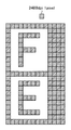
この準備動作はS202において行われる。CPU961はコントローラ904からの1ページ分の画像データ(ビットマップデータ)を取得する。図5はビットマップデータの一例を示している。解像度は2400dpiであり、画素数は14画素×21画素である。ビットマップデータは2階調の画像データである。そのため、各画素は黒画素または白画素である。
(1) Preparation of image data in memory This preparation operation is performed in S202. The
(2)PWM階調テーブルの設定
S201で実行されるPWM設定ではPWMIC905が2400dpiの1画素あたり13段階の階調テーブルを選択する。走査速度と分解能の関係から、たとえば、1画素が最大で12分割される。PWMは、APCによって決定された最大光量を感光ドラム102の表面での光量(露光量)へダイナミックに低減するために用いられる。つまり、最大光量を達成可能な駆動電流を流す期間(幅)を増減することで、露光量が調整される。
(2) Setting of PWM gradation table In the PWM setting executed in S201,
図5が示す画像は文字および線画像を含んでいるが、コントローラ904からの画像はドットスクリーン処理により2階調に面積階調処理されてからCPU961に供給される。1ページ分の画像形成中は露光量が調節されない。黒から白までの階調を10レベルで表現する場合、黒画素が10階調幅(PWMの最大幅)で表現され、白画素は0階調幅(非発光)で表現される。
The image shown in FIG. 5 includes a character and a line image. The image from the
(3)基準位置信号の発生と入力
CPU961は、モータ202を一定速で回転制御し、BD信号がほぼ一定周期で検知されるようにフィードバック制御を行う。CPU961はBD信号を割込信号として認識してビデオデータ処理を開始する。
(3) Generation and Input of Reference Position Signal The
(4)基準位置信号をトリガーとして計時を開始することによる露光位置の特定
図6を用いてCPU961が実行するBD割り込み処理の一例を説明する。BD割り込み処理は、BD信号によって発生する処理である。CPU961はBDセンサ212からBD信号を受けると、BD信号の立下りを基準として割り込みを発生する。
(4) Identification of exposure position by starting timing with reference position signal as trigger Referring to FIG. 6, an example of BD interrupt processing executed by the
S211で、CPU961は、主走査位置をカウントするカウンタ(HCLKカウンタ)をリセットする。S212で、CPU961は、水晶発振器480から画像クロックHCLKが入力されるたびにHCLKカウンタをカウントアップさせる。HCLKカウンタは、1走査の画像データ幅に対応し、一走査毎に0〜32767までのカウントアップを繰り返す。このようにCPU961はHCLKカウンタによって現在の主走査位置を特定する。
In S211, the
(5)多重露光シーケンスでの元画像データの読み出し
S213で、CPU961は、1走査中のドラム表面上の主走査位置に合わせてメモリから元画像データを読み出す。1走査での各画素データは、HCLKカウンタで特定された現在の主走査位置に対応している。8つのレーザ素子302A〜302Hに対応した8つの画素データがそれぞれメモリから読み出される。
(5) Reading of original image data in multiple exposure sequence In S213, the
(6)マルチレーザ書き出し遅延
S214で、CPU961は、各画像データについて画像クロックHCLKをカウントして遅延処理させる。図2を用いて説明したように8つのレーザ素子302A〜302Hは主走査方向に対して傾斜して配置されている。そのため、8つのレーザ素子302A〜302Hの主走査位置を一致させるためには、8つのレーザ素子302A〜302Hの配置位置に応じて主走査書き出しタイミングを遅延させる必要がある。8つのレーザ素子302A〜302Hの配置位置は、2400dpiにおいて1画素ずつずれている。よって、CPU961は、レーザ素子302A〜302Hの各遅延量をそれぞれ0ないし7に設定する。たとえば、レーザ素子302Hは、レーザ素子302Aに対して7画素分だけBD信号から遅延して同一の領域(主走査位置)を露光する。よって、レーザ素子302Hはレーザ素子302Aに対して7画素分だけ遅延して画像データを供給される。なお、遅延量はHCLKカウンタのカウント値に換算して設定される。このような遅延処理によって、45度傾斜して複数の光源が配置された光源アレイであっても、図7が例示するように、感光ドラム102の表面では2次元の画素配列の直交性が再現される。
(6) Multi-Laser Write Delay In S214, the
(7)PWMICへのデータ転送
S215で、CPU961は、CPUバス473を介してPWMIC905へ画像データを転送する。各レーザ素子に対してそれぞれ3ビットのPWMビデオデータが転送される。S216で、CPU961は、1BD周期(1つの主走査ライン)分のすべての画像データの転送が完了したかどうかを判定する。たとえば、CPU961は、HCLKカウンタのカウント値が32767になったかどうかを判定する。カウント値が32767になっていれば、1つの主走査ラインのすべての画像データが転送されたことを意味するため、CPU961はBD割込処理を終了する。カウント値が32767未満であれば、S212に戻る。
(7) Data Transfer to PWMIC In step S215, the
図7を用いて多重露光シーケンスの一例について説明する。図7において、ドラム面上の潜像とビデオデータとの対応関係が模式化されている。つまり、レーザ素子302A〜302Hと、6個のBD信号に対応した6走査S1〜S6との関係が示されている。なお、ビデオデータとはCPU961がPWMICに出力する画像データのことである。
An example of the multiple exposure sequence will be described with reference to FIG. In FIG. 7, the correspondence between the latent image on the drum surface and the video data is schematically shown. That is, the relationship between the
第1回目の走査S1では、メモリから、4ライン分(つまり4画素ずつ)の画像データが読み出され、第2光源群であるレーザ素子302E〜302Hに供給される。つまり、画像データはPWMIC905を通じて第2レーザドライバ400Bに供給される。
In the first scan S1, image data for four lines (that is, every four pixels) is read from the memory and supplied to the
第1レーザドライバ400Aで駆動される第1光源群に含まれるレーザ素子302A〜302Dによって形成される画素は黒い画素で示されている。第2レーザドライバ400Bで駆動される第2光源群に含まれるレーザ素子302E〜302Hによって形成される画素は灰色の画素で示されている。感光ドラム102は、あるBD信号が出力されてから次のBD信号が出力されるまでに副走査方向に4ライン分だけ回転する。なお、レーザ素子302A〜302Dから出射されるレーザ光に対して、レーザ素子302E〜302Hから出射されたレーザ光は、感光体の回転方向で上流側を走査するように、レーザ素子302A〜302Dとレーザ素子302E〜302Hが配置されている。
Pixels formed by the
S2では、CPU961はメモリから8ライン分の画像データを読み出して、PWMIC905を通じて第1レーザドライバ400Aおよび第2レーザドライバ400Bに供給する。つまり、S1で第2光源群のために読み出された画像データは再度読み出され、第1光源群のためのレーザ素子302A〜302Dに供給される。副走査方向に続く新しい4ライン分の画像データは第2光源群のレーザ素子302E〜302Hに供給される。S1の後半の4ライン分の画像データと、S2の前半の4ライン分の画像データとが同一の画像データであるため、第1光源群と第2光源群とによって4ラインずつ多重露光(多重走査)が実行される。
In S2, CPU961 reads the image data of 8 lines from the memory and supplies the
S3ないしS6では、S2の処理が繰り返される。つまり、8ライン分の画像データのうち第1光源群に供給される4ライン分の画像データは、1つ前のBD周期で第2光源群に供給される4ライン分の画像データと同一である。これにより、すべてのラインについて第1光源群と第2光源群とによって多重露光が実行される。 In S3 to S6, the process of S2 is repeated. That is, among the image data for 8 lines, the image data for 4 lines supplied to the first light source group is the same as the image data for 4 lines supplied to the second light source group in the previous BD cycle. is there. Thereby, multiple exposure is executed by the first light source group and the second light source group for all the lines.
このように、n走査周期目において第2光源群のレーザ素子302E〜302Hから出射されたレーザ光が露光した領域は感光体の回転によって回転方向の上流側から下流側に移動する。当該領域は、n+1走査周期目で第1光源群のレーザ素子302A〜302Dから出射されたレーザ光により露光される。
As described above, in the n-th scanning period, the region exposed by the laser light emitted from the
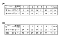
図5に示した元の画像データは164画素(多重でカウントすると328画素)からなる。図8(a)が示すように、1回目の走査から7回目の走査までで第1レーザドライバ400Aの累積画素値と第2レーザドライバ400Bの累積画素値はともに164である。つまり、第1レーザドライバ400Aが露光を担当した画素数と第2レーザドライバ400Bが露光を担当した画素数とが一致している。このように、露光処理が第1レーザドライバ400Aと第2レーザドライバ400Bとに均等に配分されている。
The original image data shown in FIG. 5 consists of 164 pixels (328 pixels when counted in multiples). As shown in FIG. 8A, the cumulative pixel value of the
(ドライバの上昇について)
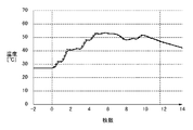
図9は連続で10枚の画像を形成した場合の第1レーザドライバ400Aの温度と第2レーザドライバ400Bの温度とを示している。第1レーザドライバ400Aの温度は実線で示されており、第2レーザドライバ400Bの温度は破線で示されている。横軸はプリント枚数を示している。縦軸はICチップの表面温度を示している。ここでは、24秒間に12枚のA4サイズのシートSに連続して画像が形成されている。
(About rising drivers)
FIG. 9 shows the temperature of the
第1レーザドライバ400Aの温度と第2レーザドライバ400Bの温度は、室温である27℃から55℃程度まで上昇している。1枚のシートSへの作像時間は約1秒であり、先行するシートSの後端から後続のシートSの先端までの紙間(非作像時間)も約1秒である。つまり、1秒ごとに加熱と放熱とが繰り返されている。その結果、12回の温度上昇によって温度はノコギリ状に変化している。12枚のプリントが完了すると、第1レーザドライバ400Aの温度と第2レーザドライバ400Bの温度は40℃程度まで緩やかに低下する。
The temperature of the
本実施形態では第1駆動ICである第1レーザドライバ400Aと第2駆動ICである第2レーザドライバ400Bには同一の画像データが供給される。そのため、第1レーザドライバ400Aの温度と第2レーザドライバ400Bの温度は連動して上昇および低下する。これは、第1光源群と第2光源群とが同一の画素を同一の画像データで露光するよう第1レーザドライバ400Aが第1光源群を制御し、第2レーザドライバ400Bが第2光源群を制御するからである。さらに、第1光源群によって第1回目の露光が実行され、第1回目の露光によって露光された位置を第2光源群による第2回目の露光することで多重露光が実行されるからでもある。図9が示すように、第1レーザドライバ400Aの温度と第2レーザドライバ400Bの温度との差は測定誤差程度の違いしかなく、両者は実質的に同一となる。
In the present embodiment, the same image data is supplied to the
(温度差にともなう光量変動)
第1レーザドライバ400A、第2レーザドライバ400B、受光素子PDおよびサイクルAPCにより構成されるAPCでは、各ドライバの温度が10℃変動すると、最大で±1%程度の制御誤差が発生しうる。駆動電流が±1%程度変動すると、光量が1%程度変動する。
(Light intensity variation with temperature difference)
In the APC configured by the
しかし、図10に示すように多重露光処理を第1レーザドライバ400Aと第2レーザドライバ400Bとに均等に配分すれば、第1レーザドライバ400Aと第2レーザドライバ400Bとの温度差はどのタイミングでも非常に小さくなる(2.5℃以下)。よって、レーザドライバ間の温度変動にともなう光量変動がほぼ0.5%以内に収まる。
However, if the multiple exposure process is equally distributed between the
ミクロに見ると、図7の例からもわかるように、多重露光における1回目の露光と2回目の露光との間には1BD周期(約1ミリ秒)の時間差がある。つまり、この時間差の分だけ第2レーザドライバ400Bが第1レーザドライバ400Aよりも先に温度変動する。しかし、図9に見られるような温度変動に対してこの時間差は非常に小さい。つまり、時間差に依存した温度差は1℃以下に過ぎない。
When viewed microscopically, as can be seen from the example of FIG. 7, there is a time difference of 1 BD period (about 1 millisecond) between the first exposure and the second exposure in the multiple exposure. That is, the temperature of the
(比較例と実施形態との比較)
図11は、比較例の構成を示している。第1レーザドライバ400Aは奇数番目のレーザ素子を駆動し、第2レーザドライバ400Bは偶数番目のレーザ素子を駆動する。つまり、比較例では、多重露光処理が第1レーザドライバ400Aと第2レーザドライバ400Bとに均等に配分されていない事例である。
(Comparison between comparative example and embodiment)
FIG. 11 shows a configuration of a comparative example. The
図12は、比較例における露光例を示している。第1レーザドライバ400Aが露光を担当する画素は黒い画素で示され、第2レーザドライバ400Bが露光を担当する画素は灰色で示されている。図8(b)は、比較例における第1レーザドライバ400Aが処理した累積画素数と、第2レーザドライバ400Bが処理した累積画素数とを示している。ここでは、7回の走査が実行されている。実施形態の累積画素数を示した図8(a)と比較すると分かるように、比較例では、第1レーザドライバ400Aが処理した累積画素数と第2レーザドライバ400Bが処理した累積画素数とが大きく乖離している。
FIG. 12 shows an exposure example in the comparative example. The pixels for which the
図13は、比較例における画像形成枚数に対する第1レーザドライバ400Aの温度と第2レーザドライバ400Bの温度とを示している。第1レーザドライバ400Aの温度は実線で示されており、第2レーザドライバ400Bの温度は破線で示されている。横軸はプリント枚数を示している。縦軸はICチップの表面温度を示している。ここでは、24秒間に12枚のA4サイズのシートSに連続して画像が形成されている。図13が示すように、第1レーザドライバ400Aの温度と第2レーザドライバ400Bの温度との差は最大で10℃程度となっている。このように温度差が大きくなると、光量変動が最大で±2%程度に拡大する。その結果、画像の濃度ムラが発生し、画質が劣化する。
FIG. 13 shows the temperature of the
本発明の構成を一般化するため、代数を次のように定義する。光源アレイを構成する光源(レーザ素子)の数をN(Nは4以上の整数)とする。1つのレーザドライバ(駆動IC)が駆動できる最大のレーザ素子数をL(Lは2以上の整数)とする。駆動ICの実装数をQ個(Qは2以上の整数)とする。多重露光回数をMとする。よって、本実施形態は、N=8、L=4、Q=2、M=2となる。 In order to generalize the configuration of the present invention, algebra is defined as follows. The number of light sources (laser elements) constituting the light source array is N (N is an integer of 4 or more). The maximum number of laser elements that can be driven by one laser driver (driving IC) is L (L is an integer of 2 or more). The number of drive ICs mounted is Q (Q is an integer of 2 or more). Let M be the number of multiple exposures. Therefore, in this embodiment, N = 8, L = 4, Q = 2, and M = 2.
ここで、Nと(L×Q)が等しい場合には、駆動ICには余剰駆動可能なレーザ素子が全くないことを意味する。つまり、駆動ICの実装効率が高くなる。また、MとQが等しく、かつ、それぞれ2である場合は、最も基本的な構成例である。 Here, when N and (L × Q) are equal, it means that there is no laser element that can be driven excessively in the drive IC. That is, the mounting efficiency of the driving IC is increased. Further, when M and Q are equal and 2 respectively, this is the most basic configuration example.
なお、第1の実施形態では、第1光源群および第2光源群は一列に並んだ1番目から2K番目までの2K個の光源を有する光源アレイの一部でああってもよい。また、第1光源群は2K個の光源のうち1番目からK番目までの光源を有している。第2光源群は2K個の光源のうちK+1番目から2K番目までの光源を有している。ここではN=2Kとなっている。図3に示した例ではK=4である。 In the first embodiment, the first light source group and the second light source group may be part of a light source array having 1K to 2K light sources arranged in a line. The first light source group has first to Kth light sources out of 2K light sources. The second light source group has K + 1 to 2K light sources out of 2K light sources. Here, N = 2K. In the example shown in FIG. 3, K = 4.
[実施形態2]
第1の実施形態では、それぞれ4つのレーザ素子を駆動可能な2つの電流駆動ICを用いた多重露光系について説明した。しかし、本発明の技術思想は他の駆動ICにも適用可能である。他の駆動ICとしては、たとえば、マルチレーザに対応したマルチチャンネル型のアナログデジタル変換ICやPWMICがある。これは、アナログデジタル変換ICの量子化性能には温度依存性があり、デジタルアナログ変換ICのアナログ出力性能にも温度依存性があるからである。同様にPWMICの発光タイミング性能にも温度依存性が存在する。よって、これらに起因した走査ムラを低減するためには、本発明の技術思想が有効である。
[Embodiment 2]
In the first embodiment, the multiple exposure system using two current drive ICs each capable of driving four laser elements has been described. However, the technical idea of the present invention can be applied to other driving ICs. As other driving ICs, for example, there are multi-channel type analog-digital conversion ICs and PWM ICs corresponding to multi-lasers. This is because the quantization performance of the analog-digital conversion IC has temperature dependence, and the analog output performance of the digital-analog conversion IC also has temperature dependence. Similarly, the temperature dependence of the emission timing performance of PWMIC also exists. Therefore, the technical idea of the present invention is effective in reducing the scanning unevenness caused by these.
図14は、第2の実施形態における8つのレーザ素子を駆動可能な駆動ICであるレーザドライバ1400A、4つのレーザ素子をサポートした駆動ICである第1のPWMIC1905Aおよび第2のPWMIC1905Bを示している。光源アレイは8つのレーザ素子302A〜302Hを有している。つまり、第1のPWMIC1905Aは第1光源群であるレーザ素子302A〜302Dをサポートし、第2のPWMIC1905Bは第2光源群であるレーザ素子302E〜302Hをサポートしている。第1光源群と第2光源群とで多重露光する点はすでに説明したとおりである。その他の点は、第1の実施形態と第2の実施形態で共通しているため説明を省略する。多重露光処理は、第1のPWMIC1905Aと第2のPWMIC1905Bとに均等に分散されるため、両者の温度差は非常に小さくなる。その結果、第1光源群と第2光源群との露光位置の差や光量のムラも非常に小さくなり、第2の実施形態でも第1の実施形態と同様の効果が得られる。上記の代数で表記すると、第2の実施形態ではN=8、L=4、Q=2、M=2となる。
FIG. 14 shows a
第1の実施形態のようなフィードバック制御系では、本発明の技術思想によって、駆動IC間の温度差が小さくなるため制御誤差ムラも減少する。これは、APCの実行頻度を緩和する。つまり、APCの実行間隔を長くすることが可能となる。また、駆動ICの温度に依存した光量変動特性についての要件も緩和される。これらは、光走査装置104の設計の自由度をもたらすだけでなく、部品の歩留まりや部品単価を改善する効果ももたらすであろう。
In the feedback control system as in the first embodiment, due to the technical idea of the present invention, the temperature difference between the drive ICs is reduced, so that the control error unevenness is also reduced. This alleviates the frequency of APC execution. That is, the APC execution interval can be lengthened. In addition, the requirement for the light quantity variation characteristic depending on the temperature of the driving IC is relaxed. These will not only provide freedom in designing the
第2の実施形態のようなPWMICについてはフィードバック制御が適用されない場合、温度による絶対精度の緩和によって、部品の歩留まりや部品単価がさらに改善されよう。 When the feedback control is not applied to the PWMIC as in the second embodiment, the yield of components and the component unit price will be further improved by relaxing the absolute accuracy due to temperature.
[実施形態3]
本発明の技術思想は図15が示すよう多重露光系にも採用可能である。図15が示すように、PWMICとして第2の実施形態で説明した第1のPWMIC1905Aと第2のPWMIC1905Bが採用されてもよい。また、レーザドライバとして第1の実施形態で説明した第1レーザドライバ400Aと第2レーザドライバ400Bが採用されてもよい。このような多重露光系であっても本発明は適用可能であり、第1の実施形態や第2の実施形態と同等の効果が期待される。
[Embodiment 3]
The technical idea of the present invention can also be applied to a multiple exposure system as shown in FIG. As shown in FIG. 15, the
[実施形態4]
上述した実施形態では、8つのレーザ素子を有する光源アレイを一例として説明したが、4つのレーザ素子を有する光源アレイや32個のレーザ素子を有する光源アレイなどにも適用可能である。つまり、光源アレイを構成するレーザ素子の数Nは、駆動ICの数Qの倍数であればよい。レーザ素子の数NがQの倍数であれば、各駆動ICが駆動を担当するレーザ素子の数が均等になるからである。
[Embodiment 4]
In the above-described embodiment, the light source array having eight laser elements has been described as an example. However, the present invention can be applied to a light source array having four laser elements, a light source array having 32 laser elements, and the like. That is, the number N of laser elements constituting the light source array may be a multiple of the number Q of drive ICs. This is because if the number N of laser elements is a multiple of Q, the number of laser elements that each drive IC is responsible for driving becomes equal.
なお、Q個の駆動ICがサポート可能なレーザ素子の総数は光源アレイに設けられているレーザ素子の数と同一でなくてもよい。これは、各駆動ICが駆動を担当するレーザ素子の数が均等になるからである。 Note that the total number of laser elements that can be supported by the Q drive ICs may not be the same as the number of laser elements provided in the light source array. This is because the number of laser elements each driving IC is responsible for driving becomes equal.
上述した実施形態では1つの画素につき2回の多重露光を実行する例を取り上げたが、1つの画素あたりの多重露光回数はQの倍数であればよい。つまり、多重露光回数は3であってもよいし、4であってもよい。多重露光回数が3であれば3個の駆動ICが必要となる。多重露光回数が4であれば2個または4個の駆動ICが必要となる。いずれも多重露光回数は駆動ICの数Qの倍数になっている。このように多重露光回数がQの倍数であれば、各駆動ICが駆動を担当するレーザ素子の数が均等になる。 In the above-described embodiment, an example in which multiple exposure is performed twice per pixel has been described. However, the number of multiple exposures per pixel may be a multiple of Q. That is, the number of multiple exposures may be 3 or 4. If the number of multiple exposures is 3, three drive ICs are required. If the number of multiple exposures is 4, 2 or 4 drive ICs are required. In both cases, the number of multiple exposures is a multiple of the number Q of driving ICs. Thus, when the number of multiple exposures is a multiple of Q, the number of laser elements that each drive IC is responsible for driving becomes equal.
ところで、画像形成装置100において、ある画像形成モードから他の画像形成モードに切り替えたときに副走査速度やビーム数が変更されることがある。たとえば、2400dpiで画像を形成する高画質モードから1200dpiで画像を形成する通常画質モードへの切り替えなどがこれに該当する。2400dpiの画像を形成するために8個のレーザ素子を使用する場合、1200dpiの画像を形成するためには4個のレーザ素子を使用すればよい。つまり、8個のレーザ素子302A〜302Hのうち奇数番目のレーザ素子302A、302C、302E、302Gだけが使用される。この場合、第1レーザドライバ400Aがレーザ素子302A、302Cの駆動を担当し、第2レーザドライバ400Bがレーザ素子302E、302Gの駆動を担当する。各駆動ICが駆動を担当するレーザ素子の数が均等になる。また、レーザ素子302A、302Eが同一の画像データによって同一の画素を多重露光し、レーザ素子302C、302Gが同一の画像データによって同一の画素を多重露光する。よって、各駆動ICによって処理される累積画素数が同一となり、各駆動ICは連動して温度の上昇と下降を繰り返すことになる。
In the
たとえば、図16が示すように光走査装置104は、18個のレーザ素子302A〜302Rを有する光源アレイ300を用いて3重露光を実行してもよい。光走査装置104は、3重露光を第1の副走査速度で行い、6重露光を第1の副走査速度の半分の第2の副走査速度で行ってもよい。回転多面鏡の回転速度は3重露光と6重露光との双方で同じである。また、主走査周期(BD周期)も3重露光と6重露光との双方で同じである。
For example, as shown in FIG. 16, the
図16が示すように、第1レーザドライバ400Aはレーザ素子302A〜302Fの駆動を担当する。第2レーザドライバ400Bはレーザ素子302G〜302Lの駆動を担当する。第3レーザドライバ400Cはレーザ素子302M〜302Rの駆動を担当する。
As shown in FIG. 16, the
6重露光においては、レーザ素子302A、302D、302G、302J、302M、302Pが1つのグループとなり、同一の主走査ラインの露光を担当する。レーザ素子302B、302E、302H、302K、302N、302Qが1つのグループとなり、同一の主走査ラインの露光を担当する。さらに、レーザ素子302C、302F、302I、302L、302O、302Rが1つのグループとなり、同一の主走査ラインの露光を担当する。
In the six-fold exposure, the
なお、各レーザドライバは最大で8個のレーザ素子の駆動を担当可能であってもよい。つまり、各レーザドライバは8つの駆動回路のうち2つの駆動回路がそれぞれ余剰となる。ただし、各レーザドライバのうち稼働する駆動回路の数は同じであり、余剰な駆動回路の数も同じである。上記の代数で表記すると、本実施形態は、N=18、L=8、Q=3、M=6となる。 Each laser driver may be capable of driving up to eight laser elements. That is, in each laser driver, two of the eight drive circuits are redundant. However, the number of drive circuits operating among the laser drivers is the same, and the number of redundant drive circuits is also the same. Expressed in the above algebra, in the present embodiment, N = 18, L = 8, Q = 3, and M = 6.
Q個の駆動ICでそれぞれL個のレーザ素子を駆動できるため、トータルでの駆動可能なレーザ素子数は(L×Q)個であるが、光源アレイに含まれるレーザ素子の数Nは、(L×Q)以下である。 Since L laser elements can be driven by Q drive ICs, the total number of laser elements that can be driven is (L × Q), but the number N of laser elements included in the light source array is ( L × Q) or less.
1つの画素を多重露光するために使用される複数のレーザ素子は各駆動ICに均等に配分される。そのため、MはQの倍数である。なお、MはQの1倍、つまりM=Qであってもよい。 A plurality of laser elements used for multiple exposure of one pixel are equally distributed to each driving IC. Therefore, M is a multiple of Q. Note that M may be 1 times Q, that is, M = Q.
[その他の実施形態]
上述した実施形態では光源アレイとしてVCSELを一例として説明したが、VCSEL以外の端部発光レーザであっても本発明は適用可能である。本発明は、上述した実施形態の構成にのみ限定されるわけではなく、特許請求の範囲に記載した各機能または本実施形態が持つ機能が達成できる構成であればどのようなものであっても適用可能である。画像形成装置100、印刷装置(プリンタ)であってもよいし、印刷機能を有するファクシミリ装置や、印刷機能、コピー機能およびスキャナ機能等を有する複合機(MFP)であってもよい。画像形成装置100は単色画像形成装置であってもよいし多色画像形成装置であってもよい。
[Other Embodiments]
In the above-described embodiment, the VCSEL has been described as an example of the light source array. However, the present invention can be applied to an edge emitting laser other than the VCSEL. The present invention is not limited to the configuration of the embodiment described above, and any configuration can be used as long as each function described in the claims or the function of the present embodiment can be achieved. Applicable. The
[まとめ]
図3などを用いて説明したように、第1レーザドライバ400Aは第1光源群であるレーザ素子302A〜302Dを駆動する第1駆動ICとして機能する。第2レーザドライバ400Bは第2光源群であるレーザ素子302E〜302Hを駆動する第2駆動ICとして機能する。図7を用いて説明したように、第2光源群が第1回目の露光を実行する。第1光源群は第2光源群による第1回目の露光によって露光された位置に対して第2回目の露光を実行する。これにより多重露光が実現される。このように多重露光処理が第1駆動ICと第2駆動ICとに均等に分配されるため、第1駆動ICと第2駆動ICとの温度差が小さくなり、走査ムラが減少する。
[Summary]
As described with reference to FIG. 3 and the like, the
多重露光を実行してもしなくてもよい。ただし、第1光源群と第2光源群とが同一の画素を同一の画像データで露光するよう第1駆動ICが第1光源群を制御し、第2駆動ICが第2光源群を制御する。これにより、第1駆動ICと第2駆動ICとの温度差が小さくなり、走査ムラが減少する。 Multiple exposure may or may not be performed. However, the first drive IC controls the first light source group and the second drive IC controls the second light source group so that the first light source group and the second light source group expose the same pixels with the same image data. . Thereby, the temperature difference between the first drive IC and the second drive IC is reduced, and the scanning unevenness is reduced.
CPU961は、第1駆動ICの温度と第2駆動ICの温度とが連動して上昇および低下するように、第1駆動ICと第2駆動ICとに同一の画像データを供給する供給部として機能する。第1駆動ICと第2駆動ICとに同一の画像データを供給することにより、結果として、第1駆動ICの温度と第2駆動ICの温度とが連動して上昇および低下するようになる。つまり、第1駆動ICと第2駆動ICとの温度差が小さくなり、走査ムラが減少する。
The
第1の実施形態では、第1光源群および第2光源群は一列に並んだ1番目から2K番目までの2K個の光源を有する光源アレイの一部である。第1光源群は1番目からK番目までの光源であるレーザ素子302A〜302Dを有し、第2光源群は2K個の光源のうちK+1番目から2K番目までの光源であるレーザ素子302E〜302Hを有している。第1レーザドライバ400Aは2K個の光源のうち1番目からK番目までの光源を駆動し、第2レーザドライバ400Bは2K個の光源のうちK+1番目から2K番目までの光源を駆動する。CPU961が第1駆動ICの温度と第2駆動ICの温度とが連動して上昇および低下するように、第1駆動ICと第2駆動ICとに同一の画像データを供給する。これにより走査ムラが減少する。
In the first embodiment, the first light source group and the second light source group are part of a light source array having 2K light sources from the first to the 2Kth arranged in a line. The first light source group includes
図7を用いて説明したように、第1レーザドライバ400Aによって駆動される1番目からK番目までの各光源と第2レーザドライバ400Bによって駆動されるK+1番目から2K番目までの各光源とが一対一で対応している。たとえば、レーザ素子302Aとレーザ素子302Eとは同一の主走査ラインを多重露光するため、一対一で対応している。CPU961は、一対一で対応している2つのレーザ素子が同一の主走査位置を多重露光するように第1レーザドライバ400Aと第2レーザドライバ400Bとに同一の画像データを供給する。これにより、第1レーザドライバ400Aと第2レーザドライバ400Bとの温度差が小さくなり、走査ムラが減少する。
As described with reference to FIG. 7, the first to Kth light sources driven by the
さらに、上述した実施形態は次のように一般化することができる。光源アレイは、一列に並んだ1番目からN番目までのN個の光源を有していればよい。Q個の駆動ICは、N個の光源のうちそれぞれN/Q個以下であるL個の光源を駆動するように構成されていればよい(ただしN>Q)。供給部は、Q個の駆動ICのそれぞれに同一の画像データを供給する。これにより、Q個の駆動ICのそれぞれの温度が連動して上昇および低下するようになるため、走査ムラが減少する。 Further, the above-described embodiment can be generalized as follows. The light source array only needs to have the first to Nth N light sources arranged in a line. The Q drive ICs may be configured to drive L light sources, each of which is N / Q or less, out of N light sources (where N> Q). The supply unit supplies the same image data to each of the Q drive ICs. As a result, the temperature of each of the Q drive ICs rises and falls in conjunction with each other, so that scanning unevenness is reduced.
Q個の駆動ICのうちそれぞれ異なる駆動ICによって駆動される複数の光源によって同一の主走査位置が多重露光されてもよい。多重露光では、同一のデータが各駆動ICで使用されるため、各駆動ICの温度変化がほぼ同一となる。これは走査ムラを減少させる上で有利である。 The same main scanning position may be subjected to multiple exposure by a plurality of light sources driven by different driving ICs among the Q driving ICs. In the multiple exposure, since the same data is used in each drive IC, the temperature change of each drive IC becomes almost the same. This is advantageous in reducing scanning unevenness.
Nが4以上の整数であれば、高級機や中級機においてレーザドライバを共用部品化しやすい。たとえば、中級機では4つのレーザチップを備えたレーザアレイが使用され、高級機では8つまたは12個のレーザチップを備えたレーザアレイが使用されることがあるからである。 If N is an integer of 4 or more, it is easy to make the laser driver a common component in high-class machines and intermediate-class machines. This is because, for example, a laser array having four laser chips is used in an intermediate machine, and a laser array having eight or twelve laser chips is used in a high-grade machine.
多重露光の回数MはQと等しいかまたはQの倍数であればよい。つまり、Q個の駆動ICが使用される場合、多重露光の回数MがQと等しいかまたはQの倍数であれば、Q個の駆動ICに多重露光処理を均等に分散させることが可能となる。その結果、各駆動ICの温度の変化が類似する。 The number M of multiple exposures may be equal to Q or a multiple of Q. That is, when Q drive ICs are used, if the number of multiple exposures M is equal to Q or a multiple of Q, multiple exposure processing can be evenly distributed to the Q drive ICs. . As a result, the change in temperature of each drive IC is similar.
Q個の駆動ICのそれぞれは、同一の主走査位置を走査するM個の光源のうちM/Q個ずつ光源を駆動する。図3では2個のレーザ素子が同一の主走査位置を走査するため、第1レーザドライバ400Aと第2レーザドライバ400Bはそれぞれ1個ずつを駆動すればよい。図16に示した事例では6個のレーザ素子が同一の主走査位置を走査するため、第1レーザドライバ400A、第2レーザドライバ400Bおよび第3レーザドライバ400Cはそれぞれ2個ずつを駆動すればよい。なお、いずれの実施形態においてもN/QはLと等しく、かつ、MとQは等しい。図3ではとりわけM=2の場合について説明した。
Each of the Q driving ICs drives M / Q light sources out of M light sources that scan the same main scanning position. In FIG. 3, since two laser elements scan the same main scanning position, the
上述したように駆動ICの一例は光源を電流駆動するレーザドライバICである。しかし、駆動ICは、光源の駆動に関与するICチップであれば十分であり、たとえば、図14を用いて説明したように、PWMICであってもよい。つまり、駆動ICは、光源を駆動する駆動電流をパルス幅変調するパルス幅変調ICであってもよい。 As described above, an example of the driving IC is a laser driver IC that drives the light source with current. However, it is sufficient that the driving IC is an IC chip involved in driving the light source. For example, as described with reference to FIG. 14, the driving IC may be a PWM IC. That is, the driving IC may be a pulse width modulation IC that performs pulse width modulation on the driving current for driving the light source.
上述したような光走査装置104を画像形成装置100に採用することにより走査ムラ(露光ムラ)が減少するため、画像の濃度ムラが減少する。
By adopting the
Claims (17)
前記半導体レーザが備える前記複数の光源のうちの第1光源群を駆動する第1駆動ICと、
前記半導体レーザが備える前記複数の光源のうちの第2光源群を駆動する第2駆動ICと
前記複数の光源から出射されたレーザ光が前記感光体上を走査するように複数の前記レーザ光を偏向する偏向手段と、
を有し、
前記第1光源群と前記第2光源群とが同一の画素の画像データに基づいて前記感光体を露光するように、当該画像データに基づいて、前記第1駆動ICが前記第1光源群を制御し、前記第2駆動ICが前記第2光源群を制御することを特徴とする光走査装置。 A semiconductor laser comprising a plurality of light sources for emitting laser light for forming an electrostatic latent image on the photoreceptor;
A first drive IC that drives a first light source group of the plurality of light sources included in the semiconductor laser;
A second driving IC that drives a second light source group of the plurality of light sources included in the semiconductor laser; and a plurality of the laser beams so that the laser beams emitted from the plurality of light sources scan the photosensitive member. Deflection means for deflecting;
Have
The first driving IC sets the first light source group based on the image data so that the first light source group and the second light source group expose the photoconductor based on the image data of the same pixel. An optical scanning device, wherein the second driving IC controls the second light source group.
前記第1光源群は前記2K個の光源のうち1番目からK番目までの光源を有し、
前記第2光源群は前記2K個の光源のうちK+1番目から2K番目までの光源を有することを特徴とする請求項1または2に記載の光走査装置。 The first light source group and the second light source group are a part of a light source array having 2K light sources from 1st to 2Kth arranged in a line,
The first light source group includes first to Kth light sources among the 2K light sources,
The second light source group optical scanning apparatus according to claim 1 or 2, characterized in that it has a light source to 2K-th from (K + 1) -th of the 2K number of light sources.
前記半導体レーザに備えられた前記2K個の光源のうち1番目からK番目までの光源を駆動する第1駆動ICと、
前記半導体レーザに備えられた前記2K個の光源のうちK+1番目から2K番目までの光源を駆動する第2駆動ICと、
前記第1駆動ICの温度と前記第2駆動ICの温度とが連動して上昇および低下するように、前記第1駆動ICと前記第2駆動ICとに同一の画像データを供給する供給部と
を有することを特徴とする光走査装置。 A semiconductor laser provided with 2K light sources from the first to the 2Kth in a row;
A first driver IC for driving first to Kth light sources among the 2K light sources provided in the semiconductor laser;
A second driving IC for driving K + 1 to 2K light sources among the 2K light sources provided in the semiconductor laser;
A supply unit that supplies the same image data to the first drive IC and the second drive IC so that the temperature of the first drive IC and the temperature of the second drive IC rise and fall in conjunction with each other; An optical scanning device comprising:
前記供給部は、一対一で対応している2つの光源が同一の主走査位置を多重露光するように前記第1駆動ICと前記第2駆動ICとに前記同一の画像データを供給することを特徴とする請求項5に記載の光走査装置。 The first to Kth light sources driven by the first drive IC correspond to the K + 1th to 2Kth light sources driven by the second drive IC on a one-to-one basis.
The supply unit supplies the same image data to the first drive IC and the second drive IC so that two light sources corresponding one-to-one perform multiple exposure at the same main scanning position. The optical scanning device according to claim 5 , wherein:
前記半導体レーザに備えられた前記N個の光源のうちそれぞれN/Q個以下のL個の光源を駆動するQ個の駆動ICと(ただしN>Q)、
前記Q個の駆動ICのそれぞれの温度が連動して上昇および低下するように、前記Q個の駆動ICのそれぞれに同一の画像データを供給する供給部と
を有することを特徴とする光走査装置。 A semiconductor laser comprising N light sources from the first to the Nth in a row;
Q drive ICs for driving L light sources of N / Q or less among the N light sources provided in the semiconductor laser (where N> Q),
An optical scanning apparatus comprising: a supply unit that supplies the same image data to each of the Q drive ICs so that the temperature of each of the Q drive ICs rises and falls in conjunction with each other. .
前記光走査装置によって露光されることによって静電潜像が形成される感光体と
を有し、
前記光走査装置は、
一列に並んだ1番目からN番目までのN個の光源を備えた半導体レーザと、
前記半導体レーザに備えられた前記N個の光源のうちそれぞれN/Q個以下のL個の光源を駆動するQ個の駆動ICと、
前記Q個の駆動ICのそれぞれの温度が連動して上昇および低下するように、前記Q個の駆動ICのそれぞれに同一の画像データを供給する供給部と
を有することを特徴とする画像形成装置。 An optical scanning device;
A photosensitive member on which an electrostatic latent image is formed by being exposed by the optical scanning device,
The optical scanning device includes:
A semiconductor laser having N light sources from the first to the Nth in a row;
Q drive ICs for driving L light sources of N / Q or less among the N light sources provided in the semiconductor laser;
An image forming apparatus comprising: a supply unit that supplies the same image data to each of the Q drive ICs so that the temperature of each of the Q drive ICs rises and falls in conjunction with each other. .
Priority Applications (2)
| Application Number | Priority Date | Filing Date | Title |
|---|---|---|---|
| JP2013256443A JP6315967B2 (en) | 2013-12-11 | 2013-12-11 | Optical scanning device and image forming apparatus using the same |
| US14/557,118 US9557679B2 (en) | 2013-12-11 | 2014-12-01 | Image forming apparatus employing optical scanning apparatus that scans using multiple beams of light emitted from multiple light sources driven by multiple driving ICs |
Applications Claiming Priority (1)
| Application Number | Priority Date | Filing Date | Title |
|---|---|---|---|
| JP2013256443A JP6315967B2 (en) | 2013-12-11 | 2013-12-11 | Optical scanning device and image forming apparatus using the same |
Publications (3)
| Publication Number | Publication Date |
|---|---|
| JP2015114491A JP2015114491A (en) | 2015-06-22 |
| JP2015114491A5 JP2015114491A5 (en) | 2017-01-26 |
| JP6315967B2 true JP6315967B2 (en) | 2018-04-25 |
Family
ID=53271062
Family Applications (1)
| Application Number | Title | Priority Date | Filing Date |
|---|---|---|---|
| JP2013256443A Active JP6315967B2 (en) | 2013-12-11 | 2013-12-11 | Optical scanning device and image forming apparatus using the same |
Country Status (2)
| Country | Link |
|---|---|
| US (1) | US9557679B2 (en) |
| JP (1) | JP6315967B2 (en) |
Families Citing this family (5)
| Publication number | Priority date | Publication date | Assignee | Title |
|---|---|---|---|---|
| JP6317610B2 (en) | 2014-04-03 | 2018-04-25 | キヤノン株式会社 | Image forming apparatus |
| JP6225973B2 (en) | 2015-10-20 | 2017-11-08 | ブラザー工業株式会社 | Image forming apparatus |
| US9983502B2 (en) | 2015-11-20 | 2018-05-29 | Canon Kabushiki Kaisha | Controller |
| JP7107013B2 (en) * | 2018-06-19 | 2022-07-27 | コニカミノルタ株式会社 | Optical recording device and image forming device |
| JP7102268B2 (en) * | 2018-07-10 | 2022-07-19 | 東芝テック株式会社 | Image forming device and correction method |
Family Cites Families (10)
| Publication number | Priority date | Publication date | Assignee | Title |
|---|---|---|---|---|
| US5808656A (en) * | 1993-09-15 | 1998-09-15 | Oce Printing Systems Gmbh | Arrangement and process for generating a matrix image on a photosensitive recording substrate |
| JP2004021208A (en) * | 2002-06-20 | 2004-01-22 | Noritsu Koki Co Ltd | Photoprocessing system |
| JP4366256B2 (en) | 2003-07-14 | 2009-11-18 | キヤノン株式会社 | Light beam scanning image forming apparatus |
| JP5016853B2 (en) | 2006-06-09 | 2012-09-05 | キヤノン株式会社 | Image forming apparatus and laser light quantity correction method |
| JP5407880B2 (en) * | 2010-01-13 | 2014-02-05 | 株式会社リコー | Optical scanning apparatus and image forming apparatus |
| JP5792960B2 (en) * | 2010-01-28 | 2015-10-14 | キヤノン株式会社 | Image forming apparatus |
| JP5783688B2 (en) * | 2010-07-02 | 2015-09-24 | キヤノン株式会社 | Image forming apparatus |
| JP5605042B2 (en) * | 2010-07-15 | 2014-10-15 | 株式会社リコー | Semiconductor laser driving device and image forming apparatus provided with the driving device |
| JP6029315B2 (en) | 2012-04-26 | 2016-11-24 | キヤノン株式会社 | Image forming apparatus |
| JP2013228609A (en) | 2012-04-26 | 2013-11-07 | Canon Inc | Image forming device |
-
2013
- 2013-12-11 JP JP2013256443A patent/JP6315967B2/en active Active
-
2014
- 2014-12-01 US US14/557,118 patent/US9557679B2/en active Active
Also Published As
| Publication number | Publication date |
|---|---|
| US20150160582A1 (en) | 2015-06-11 |
| JP2015114491A (en) | 2015-06-22 |
| US9557679B2 (en) | 2017-01-31 |
Similar Documents
| Publication | Publication Date | Title |
|---|---|---|
| US7528853B2 (en) | Color image forming apparatus and process cartridge | |
| JP4341908B2 (en) | Pixel clock and pulse modulation signal generation apparatus, optical scanning apparatus, and image forming apparatus | |
| JP6315967B2 (en) | Optical scanning device and image forming apparatus using the same | |
| JP5078836B2 (en) | Optical scanning apparatus and image forming apparatus | |
| US9746795B2 (en) | Optical writing control device, image forming apparatus, and optical writing control method for controlling light emission of a light source | |
| US8199376B2 (en) | Image forming apparatus and image forming method | |
| US9575432B2 (en) | Image forming apparatus | |
| US7088381B2 (en) | Image forming apparatus and method of controlling the image forming apparatus | |
| US8125504B2 (en) | Image forming apparatus and control program of image forming apparatus | |
| JP2007245448A (en) | Image forming apparatus | |
| JP2006251242A (en) | Optical scanner, method of optical scanning and optical scanning program | |
| JP2016141099A (en) | Optical scanning device and image forming device | |
| JP2004354626A (en) | Image forming apparatus and method for generating horizontal synchronous signal thereof | |
| JP2006116716A (en) | Optical scanner, pixel clock generation method of optical scanner and image forming apparatus | |
| JP2004174915A (en) | Image formation apparatus | |
| JP4866057B2 (en) | Optical device, image forming apparatus, and lighting position changing method | |
| JP2009214454A (en) | Multi-beam scanning apparatus | |
| JP2000071516A (en) | Image forming apparatus | |
| JP2000292720A (en) | Image forming device | |
| JP2003161902A (en) | Image forming apparatus | |
| JP2002225346A (en) | Imaging apparatus | |
| JP2006159560A (en) | Image forming apparatus | |
| JPH11105338A (en) | Image-forming apparatus | |
| JP2003276239A (en) | Imaging apparatus | |
| US20140036021A1 (en) | Optical scanning device, optical scanning device control method, and image forming apparatus |
Legal Events
| Date | Code | Title | Description |
|---|---|---|---|
| A521 | Written amendment |
Free format text: JAPANESE INTERMEDIATE CODE: A523 Effective date: 20161209 |
|
| A621 | Written request for application examination |
Free format text: JAPANESE INTERMEDIATE CODE: A621 Effective date: 20161209 |
|
| A977 | Report on retrieval |
Free format text: JAPANESE INTERMEDIATE CODE: A971007 Effective date: 20170912 |
|
| A131 | Notification of reasons for refusal |
Free format text: JAPANESE INTERMEDIATE CODE: A131 Effective date: 20170925 |
|
| A521 | Written amendment |
Free format text: JAPANESE INTERMEDIATE CODE: A523 Effective date: 20170928 |
|
| TRDD | Decision of grant or rejection written | ||
| A01 | Written decision to grant a patent or to grant a registration (utility model) |
Free format text: JAPANESE INTERMEDIATE CODE: A01 Effective date: 20180226 |
|
| A61 | First payment of annual fees (during grant procedure) |
Free format text: JAPANESE INTERMEDIATE CODE: A61 Effective date: 20180327 |
|
| R151 | Written notification of patent or utility model registration |
Ref document number: 6315967 Country of ref document: JP Free format text: JAPANESE INTERMEDIATE CODE: R151 |