JP6317610B2 - Image forming apparatus - Google Patents
Image forming apparatus Download PDFInfo
- Publication number
- JP6317610B2 JP6317610B2 JP2014077259A JP2014077259A JP6317610B2 JP 6317610 B2 JP6317610 B2 JP 6317610B2 JP 2014077259 A JP2014077259 A JP 2014077259A JP 2014077259 A JP2014077259 A JP 2014077259A JP 6317610 B2 JP6317610 B2 JP 6317610B2
- Authority
- JP
- Japan
- Prior art keywords
- light emitting
- laser
- light
- emitting points
- image forming
- Prior art date
- Legal status (The legal status is an assumption and is not a legal conclusion. Google has not performed a legal analysis and makes no representation as to the accuracy of the status listed.)
- Active
Links
Images


Classifications
-
- G—PHYSICS
- G03—PHOTOGRAPHY; CINEMATOGRAPHY; ANALOGOUS TECHNIQUES USING WAVES OTHER THAN OPTICAL WAVES; ELECTROGRAPHY; HOLOGRAPHY
- G03G—ELECTROGRAPHY; ELECTROPHOTOGRAPHY; MAGNETOGRAPHY
- G03G15/00—Apparatus for electrographic processes using a charge pattern
- G03G15/04—Apparatus for electrographic processes using a charge pattern for exposing, i.e. imagewise exposure by optically projecting the original image on a photoconductive recording material
- G03G15/043—Apparatus for electrographic processes using a charge pattern for exposing, i.e. imagewise exposure by optically projecting the original image on a photoconductive recording material with means for controlling illumination or exposure
-
- B—PERFORMING OPERATIONS; TRANSPORTING
- B41—PRINTING; LINING MACHINES; TYPEWRITERS; STAMPS
- B41J—TYPEWRITERS; SELECTIVE PRINTING MECHANISMS, i.e. MECHANISMS PRINTING OTHERWISE THAN FROM A FORME; CORRECTION OF TYPOGRAPHICAL ERRORS
- B41J2/00—Typewriters or selective printing mechanisms characterised by the printing or marking process for which they are designed
- B41J2/435—Typewriters or selective printing mechanisms characterised by the printing or marking process for which they are designed characterised by selective application of radiation to a printing material or impression-transfer material
- B41J2/447—Typewriters or selective printing mechanisms characterised by the printing or marking process for which they are designed characterised by selective application of radiation to a printing material or impression-transfer material using arrays of radiation sources
- B41J2/45—Typewriters or selective printing mechanisms characterised by the printing or marking process for which they are designed characterised by selective application of radiation to a printing material or impression-transfer material using arrays of radiation sources using light-emitting diode [LED] or laser arrays
-
- B—PERFORMING OPERATIONS; TRANSPORTING
- B41—PRINTING; LINING MACHINES; TYPEWRITERS; STAMPS
- B41J—TYPEWRITERS; SELECTIVE PRINTING MECHANISMS, i.e. MECHANISMS PRINTING OTHERWISE THAN FROM A FORME; CORRECTION OF TYPOGRAPHICAL ERRORS
- B41J2/00—Typewriters or selective printing mechanisms characterised by the printing or marking process for which they are designed
- B41J2/435—Typewriters or selective printing mechanisms characterised by the printing or marking process for which they are designed characterised by selective application of radiation to a printing material or impression-transfer material
- B41J2/447—Typewriters or selective printing mechanisms characterised by the printing or marking process for which they are designed characterised by selective application of radiation to a printing material or impression-transfer material using arrays of radiation sources
- B41J2/455—Typewriters or selective printing mechanisms characterised by the printing or marking process for which they are designed characterised by selective application of radiation to a printing material or impression-transfer material using arrays of radiation sources using laser arrays, the laser array being smaller than the medium to be recorded
-
- G—PHYSICS
- G03—PHOTOGRAPHY; CINEMATOGRAPHY; ANALOGOUS TECHNIQUES USING WAVES OTHER THAN OPTICAL WAVES; ELECTROGRAPHY; HOLOGRAPHY
- G03G—ELECTROGRAPHY; ELECTROPHOTOGRAPHY; MAGNETOGRAPHY
- G03G15/00—Apparatus for electrographic processes using a charge pattern
- G03G15/04—Apparatus for electrographic processes using a charge pattern for exposing, i.e. imagewise exposure by optically projecting the original image on a photoconductive recording material
- G03G15/04036—Details of illuminating systems, e.g. lamps, reflectors
- G03G15/04045—Details of illuminating systems, e.g. lamps, reflectors for exposing image information provided otherwise than by directly projecting the original image onto the photoconductive recording material, e.g. digital copiers
- G03G15/04072—Details of illuminating systems, e.g. lamps, reflectors for exposing image information provided otherwise than by directly projecting the original image onto the photoconductive recording material, e.g. digital copiers by laser
-
- G—PHYSICS
- G03—PHOTOGRAPHY; CINEMATOGRAPHY; ANALOGOUS TECHNIQUES USING WAVES OTHER THAN OPTICAL WAVES; ELECTROGRAPHY; HOLOGRAPHY
- G03G—ELECTROGRAPHY; ELECTROPHOTOGRAPHY; MAGNETOGRAPHY
- G03G2215/00—Apparatus for electrophotographic processes
- G03G2215/04—Arrangements for exposing and producing an image
- G03G2215/0402—Exposure devices
- G03G2215/0404—Laser
Description
本発明は、電子写真方式の画像形成装置に関するものである。 The present invention relates to an electrophotographic image forming apparatus.
従来、光源から出射された光ビームを回転多面鏡によって偏向するとともに、偏向した光ビームによって感光体を走査することで、感光体上に静電潜像を形成する画像形成装置が知られている。このような画像形成装置は、回転多面鏡によって偏向された光ビームを検出するための光学センサ(ビーム検出(BD)センサ)を備えており、当該光学センサは、光ビームを検出すると同期信号を生成する。画像形成装置は、光学センサによって生成される同期信号を基準として定めたタイミングに、光源から光ビームを出射させることで、光ビームが感光体上を走査する方向(主走査方向)における静電潜像(画像)の書き出し位置を一定とする。 2. Description of the Related Art Conventionally, there is known an image forming apparatus that forms an electrostatic latent image on a photosensitive member by deflecting a light beam emitted from a light source with a rotating polygon mirror and scanning the photosensitive member with the deflected light beam. . Such an image forming apparatus includes an optical sensor (beam detection (BD) sensor) for detecting a light beam deflected by a rotating polygon mirror, and the optical sensor generates a synchronization signal when the light beam is detected. Generate. The image forming apparatus emits a light beam from a light source at a timing determined with reference to a synchronization signal generated by an optical sensor, so that an electrostatic latent image in a direction in which the light beam scans on the photoconductor (main scanning direction). The writing start position of the image (image) is constant.
また、画像形成速度の高速化及び画像の高解像度化を実現するために、感光体上でそれぞれ異なるラインを並列に走査する複数の光ビームを出射する複数の発光点(発光素子)を光源として備える画像形成装置が知られている。このようなマルチビーム方式の画像形成装置では、複数の光ビームで複数のラインを並列に走査することで画像形成速度の高速化を実現するとともに、副走査方向におけるライン間の間隔を調整することによって、画像の高解像度化を実現する。 In addition, in order to realize high image forming speed and high image resolution, a plurality of light emitting points (light emitting elements) that emit a plurality of light beams that scan different lines in parallel on the photosensitive member are used as light sources. An image forming apparatus is known. In such a multi-beam type image forming apparatus, a plurality of lines are scanned in parallel with a plurality of light beams to increase the image forming speed and adjust the spacing between the lines in the sub-scanning direction. As a result, higher resolution of the image is realized.
特許文献1には、複数の発光点(発光素子)を光源として備え、当該複数の発光点が配置された平面内で光源を回転調整することで、副走査方向の解像度を調整可能な画像形成装置が開示されている。このような解像度の調整は、画像形成装置の組立工程において行われる。特許文献1には、組立工程における光源の取り付け誤差によって生じる、主走査方向の静電潜像の書き出し位置のずれを抑えるための技術が開示されている。具体的には、画像形成装置は、第1の発光点及び第2の発光点のそれぞれから出射される光ビームをBDセンサで検出して、複数のBD信号を生成する。更に、画像形成装置は、生成した複数のBD信号の生成タイミング差に基づいて、第1の発光点の光ビームの出射タイミングに対する、第2の発光点の光ビームの相対的な出射タイミングを設定する。これにより、組立工程における光源の取り付け誤差を補償して、発光点間の静電潜像の書き出し位置のずれを抑えている。 Patent Document 1 includes a plurality of light emitting points (light emitting elements) as light sources, and image formation capable of adjusting the resolution in the sub-scanning direction by rotating and adjusting the light sources in a plane in which the light emitting points are arranged. An apparatus is disclosed. Such resolution adjustment is performed in the assembly process of the image forming apparatus. Patent Document 1 discloses a technique for suppressing a shift in the writing position of an electrostatic latent image in the main scanning direction, which is caused by a light source mounting error in an assembly process. Specifically, the image forming apparatus detects a light beam emitted from each of the first light emission point and the second light emission point with a BD sensor, and generates a plurality of BD signals. Further, the image forming apparatus sets a relative emission timing of the light beam at the second light emission point with respect to the emission timing of the light beam at the first light emission point, based on the generation timing difference between the plurality of generated BD signals. To do. This compensates for the light source mounting error in the assembly process and suppresses the deviation of the electrostatic latent image writing position between the light emitting points.
また、上述のように複数の発光点(発光素子)を光源として備える画像形成装置では、当該複数の発光点を、1つのレーザ駆動IC(レーザドライバIC)で駆動する場合と、複数のレーザ駆動ICで駆動する場合とがある。例えば、特許文献2には、複数のレーザ駆動IC間で制御状態を相互にモニタリング可能とし、モニタリング結果に基づいて各レーザ駆動ICがAPCを実行するタイミングを制御する手法が提案されている。
In the image forming apparatus including a plurality of light emitting points (light emitting elements) as a light source as described above, the plurality of light emitting points are driven by one laser driving IC (laser driver IC), and a plurality of laser drivings are performed. It may be driven by an IC. For example,
上述のように、複数の発光点を光源として備える画像形成装置で、BDセンサによって生成される2つのBD信号の生成タイミング差(BD信号の時間間隔)を測定する場合、BDセンサに入射する光ビームの光量を一定にする必要がある。一般に、BDセンサに光ビームが入射した際のBDセンサの応答速度は、入射光量に応じて変化する。このため、BD信号の時間間隔の測定に用いる2つ光ビームの、BDセンサへの入射光量にばらつきがあると、BDセンサによって生成されるパルス(BD信号)の時間間隔の測定結果にばらつきが生じ、測定誤差が生じうる。したがって、BD信号の時間間隔の測定を行う場合には、発光点から出射される光ビームの光量を一定にすることで、BDセンサへ入射する光ビームの光量を一定にする必要がある。 As described above, in an image forming apparatus having a plurality of light emitting points as a light source, when measuring a generation timing difference between two BD signals generated by a BD sensor (time interval of BD signals), light incident on the BD sensor It is necessary to make the light quantity of the beam constant. In general, the response speed of the BD sensor when a light beam is incident on the BD sensor changes according to the amount of incident light. For this reason, if there is a variation in the amount of light incident on the BD sensor of the two light beams used for measuring the time interval of the BD signal, the measurement result of the time interval of the pulse (BD signal) generated by the BD sensor will vary. Measurement errors may occur. Therefore, when measuring the time interval of the BD signal, it is necessary to make the light quantity of the light beam incident on the BD sensor constant by making the light quantity of the light beam emitted from the light emitting point constant.
しかし、発光点を駆動するレーザ駆動ICの温度上昇に起因して、第1及び第2のBD信号の時間間隔(BD間隔)の測定を実行する際に当該測定に用いる2つの発光点から出射される第1及び第2の光ビームの光量が変動するおそれがある。具体的には、第1のBD信号に対応する第1の発光点を駆動するタイミングと、第2のBD信号に対応する第2の発光点を駆動するタイミングとで、レーザ駆動ICの温度が大きく異なると、第1及び2の発光点にそれぞれ供給する駆動電流の大きさにばらつきが生じる。これは、レーザ駆動ICの温度が上昇すると、レーザ駆動IC内の寄生抵抗の値の上昇等に起因して、レーザ駆動ICから出力される駆動電流が減少するためである。 However, when the measurement of the time interval (BD interval) of the first and second BD signals is executed due to the temperature rise of the laser driving IC that drives the light emitting point, the light is emitted from the two light emitting points used for the measurement. There is a possibility that the light amounts of the first and second light beams to be varied. Specifically, the temperature of the laser driving IC is determined by the timing for driving the first light emitting point corresponding to the first BD signal and the timing for driving the second light emitting point corresponding to the second BD signal. If they differ greatly, there will be variations in the magnitudes of the drive currents supplied to the first and second light emitting points, respectively. This is because when the temperature of the laser drive IC rises, the drive current output from the laser drive IC decreases due to an increase in the value of the parasitic resistance in the laser drive IC.
したがって、BD間隔の測定の際には、第1のBD信号に対応する第1の発光点を駆動するタイミングと、第2のBD信号に対応する第2の発光点を駆動するタイミングとにおいて、レーザ駆動ICの温度をできるだけ一定にする必要がある。特に、特許文献2のように複数の発光点を複数のレーザ駆動ICで駆動する場合、BD間隔の測定に用いる第1及び第2の発光点へ供給する駆動電流の差を抑制するために、画像データに基づいて各発光点を発光させる駆動制御以外の駆動制御において、複数のレーザ駆動IC間で発光点の駆動制御を極力均一に実行する必要がある。
Therefore, when measuring the BD interval, the timing for driving the first light emitting point corresponding to the first BD signal and the timing for driving the second light emitting point corresponding to the second BD signal are as follows: It is necessary to keep the temperature of the laser driving IC as constant as possible. In particular, when driving a plurality of light emitting points with a plurality of laser drive ICs as in
本発明は、上述の課題に鑑みてなされたものである。本発明は、複数の発光点を備える画像形成装置で、2つの発光点からそれぞれ出射される光ビームに対応する検出信号(BD信号)の時間間隔を測定する際に、各光ビームの光量のばらつきを低減することで測定誤差を低減する技術を提供することを目的としている。 The present invention has been made in view of the above-described problems. The present invention provides an image forming apparatus having a plurality of light emitting points, and measures the amount of light of each light beam when measuring the time interval of detection signals (BD signals) corresponding to the light beams respectively emitted from the two light emitting points. It aims at providing the technique which reduces a measurement error by reducing dispersion | variation.
本発明は、例えば、画像形成装置として実現できる。本発明の一態様の係る画像形成装置は、感光体を露光するためのレーザ光をそれぞれが出射する複数の発光点を備える光源と、前記複数の発光点から出射された複数のレーザ光が前記感光体を走査するよう、当該複数のレーザ光を偏向する偏向手段と、前記偏向手段によって偏向されたレーザ光が入射する位置に設けられ、前記偏向手段によって偏向されたレーザ光が入射すると当該レーザ光を検出したことを示す検出信号を生成するビーム検出手段と、それぞれが前記複数の発光点のうちの2つ以上の発光点に駆動電流を供給する複数のレーザドライバICであって、それぞれが異なる発光点を駆動対象とする、前記複数のレーザドライバICと、前記複数の発光点のうちで、異なるレーザドライバICによる駆動対象となっている第1及び第2の発光点が第1及び第2のレーザ光を順に出射するよう、前記第1及び第2の発光点をそれぞれ駆動対象とする第1及び第2のレーザドライバICを制御し、前記ビーム検出手段によって生成される、前記第1及び第2のレーザ光に対応する2つの検出信号の時間間隔を測定する測定手段と、前記測定手段によって測定された前記時間間隔に基づいて、前記複数の発光素子のそれぞれの、画像データに基づくレーザ光の相対的な出射タイミングを制御する制御手段と、を備えることを特徴とする。 The present invention can be realized as an image forming apparatus, for example. An image forming apparatus according to an aspect of the present invention includes a light source including a plurality of light emitting points each emitting laser light for exposing a photosensitive member, and a plurality of laser lights emitted from the plurality of light emitting points. to scan the photosensitive member, and deflecting means for deflecting the plurality of laser beams, the laser beam deflected by said deflecting means is provided at a position of incidence, the laser when the laser beam deflected by said deflecting means is incident a beam detection means for generating a detection signal indicating the detection of the light, a plurality of the laser driver IC supplies a driving current to two or more light emitting points of each of the plurality of light emitting points, respectively different light emitting points to be driven, wherein a plurality of the laser driver IC, among the plurality of light emitting points, different first及which is a driven by a laser driver IC As the second light-emitting point emits a first and a second laser beam in order to control the first and second laser driver IC to the first and second respectively driven light emitting points, the beam Measurement means for measuring a time interval between two detection signals corresponding to the first and second laser beams generated by the detection means; and the plurality of the plurality of time intervals based on the time interval measured by the measurement means. And a control means for controlling the relative emission timing of the laser light based on the image data of each of the light emitting elements.
本発明によれば、複数の発光点を備える画像形成装置で、2つの発光点からそれぞれ出射される光ビームに対応する検出信号(BD信号)の時間間隔を測定する際に、各光ビームの光量のばらつきを低減することで測定誤差を低減できる。 According to the present invention, when measuring a time interval of detection signals (BD signals) corresponding to light beams respectively emitted from two light emitting points in an image forming apparatus including a plurality of light emitting points, Measurement errors can be reduced by reducing variations in the amount of light.
以下、本発明を実施するための形態について図面を用いて説明する。なお、以下の実施形態は特許請求の範囲に係る発明を限定するものでなく、また実施形態で説明されている特徴の組み合わせの全てが発明の解決手段に必須のものとは限らない。 Hereinafter, embodiments for carrying out the present invention will be described with reference to the drawings. The following embodiments do not limit the invention according to the claims, and all combinations of features described in the embodiments are not necessarily essential to the solution means of the invention.
[第1の実施例]
<画像形成装置>
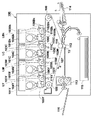
以下、電子写真方式のカラー画像形成装置を例に第1乃至第4の実施例を説明する。図1は、カラー画像形成装置の概略断面図である。図1に示す画像形成装置100は、複数色のトナーを用いて画像形成するフルカラープリンタである。なお、以下の説明では、画像形成装置の一例としてフルカラープリンタを例に挙げて説明するが、他の画像形成装置、例えば、単色(例えば、ブラック)のトナーで画像形成するモノクロプリンタ、読取装置を備えるカラーあるいはモノクロの複写機であってもよい。
[First embodiment]
<Image forming apparatus>
In the following, first to fourth embodiments will be described taking an electrophotographic color image forming apparatus as an example. FIG. 1 is a schematic sectional view of a color image forming apparatus. An
図1において、画像形成装置100は、各色毎に画像を形成する画像形成部(画像形成手段)101Y、101M、101C、及び101Bkを有している。画像形成部101Y、101M、101C、及び101Bkは、それぞれイエロー(Y)、マゼンタ(M)、シアン(C)、及びブラック(Bk)のトナーを用いて画像形成を行う。
In FIG. 1, an
画像形成部101Y、101M、101C、及び101Bkにはそれぞれ感光体である感光ドラム102Y、102M、102C、及び102Bkが備えられている。感光ドラム102Y、102M、102C、及び102Bkの周囲には、それぞれ帯電装置103Y、103M、103C、及び103Bk、光走査装置104Y、104M、104C、及び104Bk、及び現像装置105Y、105M、105C、及び105Bkが配置されている。
The
さらに、感光ドラム102Y、102M、102C、及び102Bkの周囲には、ドラムクリーニング装置106Y、106M、106C、及び106Bkが配置されている。
Further,
感光ドラム102Y、102M、102C、及び102Bkの下側には、無端状の中間転写ベルト107(中間転写体)が配置されている。中間転写ベルト107は、駆動ローラ108と従動ローラ109及び110とによって張架され、画像形成中において図1に示す矢印Bの方向に回転駆動される。また、中間転写ベルト107を介して、感光ドラム102Y、102M、102C、及び102Bkに対向する位置には、それぞれ一次転写装置111Y、111M、111C、及び111Bkが配置されている。
An endless intermediate transfer belt 107 (intermediate transfer member) is disposed below the
また、画像形成装置100には、中間転写ベルト107上のトナー像を記録媒体Sに転写するための2次転写装置112が備えられるとともに、記録媒体S上のトナー像を定着するための定着装置113が備えられている。
In addition, the
続いて、画像形成装置100における画像形成プロセスについて説明する。なお、画像形成部101Y、101M、101C、及び101Bkの各々における画像形成プロセスは同一である。このため、ここでは画像形成部101Yを例に挙げて説明し、画像形成部101M、101C、及び101Bkにおける画像形成プロセスについては説明を省略する。
Next, an image forming process in the
まず、帯電装置103Yによって、図1において矢印で示す回転方向に回転駆動する感光ドラム102Yの表面が均一に帯電される。そして、帯電された感光ドラム102Yは、光走査装置104Yから出射されるレーザ光LY(光ビーム)によって露光される。これによって、感光ドラム102Y上に静電潜像が形成される。その後、当該静電潜像は現像装置105Yによって現像され、感光ドラム102Y上にイエローのトナー像が形成される。
First, the surface of the
一次転写装置111Y、111M、111C、及び111Bkは、中間転写ベルト107に転写バイアスを印加する。これによって、感光ドラム102Y、102M、102C、及び102Bk上のイエロー、マゼンタ、シアン、ブラックのトナー像が中間転写ベルト107に転写される。この結果、中間転写ベルト107にマルチカラー(カラー)トナー像が形成される。
The
中間転写ベルト107上のカラートナー像は、2次転写装置112によって、手差し給送カセット114又は給紙カセット115から2次転写部T2に搬送された記録媒体S上に転写される。そして、記録媒体S上のカラートナー像は、定着装置113で加熱定着され、その後、記録媒体Sは排紙部116に排紙される。
The color toner image on the
なお、中間転写ベルト107に転写されずに感光ドラム102Y、102M、102C、及び102Bkに残留した残留トナーは、それぞれドラムクリーニング装置106Y、106M、106C、及び106Bkによって除去される。その後、上述の画像形成プロセスが再び実行される。
The residual toner that has not been transferred to the
<光走査装置>
図2は、光走査装置104Y、104M、104C、104Bkの概略構成図である。各光走査装置は、同一構成であるため、図2(及び後述する図3)では、光走査装置104Yを例示する。図2において半導体レーザ200から出射した発散光であるレーザ光は、コリメータレンズ201によって略平行光とされ、絞り202によってレーザ光の通過が制限される。これによりレーザ光が成形される。絞り202を通過したレーザ光は、ビームスプリッタ203に入射する。ビームスプリッタ203は、絞り202を通過したレーザ光を、フォトダイオード(PD)204に入射するレーザ光と、偏向手段の一例である回転多面鏡205(以下、ポリゴンミラー205。)に入射するレーザ光とに分離する。PD204は、レーザ光を受光することによって、受光したレーザ光の光量に応じた値(電圧)の検出信号を出力する。
<Optical scanning device>
FIG. 2 is a schematic configuration diagram of the
ビームスプリッタ203を通過したレーザ光は、シリンドリカルレンズ206を通過してポリゴンミラー205に入射する。ポリゴンミラー205は、複数の反射面(本実施例では4面)を備える。ポリゴンミラー205は、モータ207によって駆動されることで矢印Cの方向に回転する。ポリゴンミラー205は、レーザ光が感光ドラム102Yを矢印Dの方向に走査するように、レーザ光を偏向する。ポリゴンミラー205によって偏向されたレーザ光は、fθ特性を有する結像光学系(fθレンズ)208を透過し、ミラー209を介して感光ドラム102Y上(感光体上)に導かれる。このように、ポリゴンミラー205は、半導体レーザ200(図3の複数の発光点301〜308)から出射された複数のレーザ光が感光ドラム102Yを走査するよう、当該複数のレーザ光を偏向する。
The laser light that has passed through the
光走査装置104Yは、ビーム検出(BD)センサ210を備える。BDセンサ210は、レーザ光の走査経路上の、ポリゴンミラー205によって偏向されたレーザ光が入射する位置であって、感光ドラム102Y上の画像形成領域から外れた位置に配置されている。BDセンサ210は、ポリゴンミラー205によって偏向されたレーザ光を受光したことに応じて、レーザ光を検出したことを示す検出信号(BD信号)を、(水平)同期信号として生成及び出力する。
The
<レーザ光源>
次に、光走査装置104Y、104M、104C、104Bkが備える光源(レーザ光源)について説明する。図3(a)は、図2に示す半導体レーザ200が備える複数の発光点を示しており、図3(b)は、当該複数の発光点からレーザ光が同時に出射された場合の、感光ドラム102Y上におけるレーザスポットの配列イメージを示す図である。
<Laser light source>
Next, a light source (laser light source) included in the
図3(a)に示すように、半導体レーザ200は、複数(本実施例では8個)の発光点301〜308を備える垂直共振器型面発光レーザ(VCSEL:Vertical Cavity Surface Emitting Laser)である。なお、半導体レーザとして、VCSELだけでなく、端面発光型の半導体レーザが用いられてもよい。本実施例は、半導体レーザ200が8個の発光点を備える場合だけでなく、2以上の任意の数(例えば32個)の発光点を備える場合について同様に適用できる。
As shown in FIG. 3A, the
発光点301〜308は、基板上にアレイ状に配置されている。図3(a)のように各発光点が配列されているため、各発光点を同時に点灯させた場合、各発光点から出射されたレーザ光L1〜L8は、図3(b)の結像位置S1〜S8のように、主走査方向において感光ドラム102Y上の異なる位置を露光する。また、各発光点を同時に点灯させた場合、各発光点から出射されたレーザ光L1〜L8は、図3(b)の結像位置S1〜S8のように副走査方向において異なる位置を露光する。なお、図3(a)では、複数の発光点が一列に配置された例(一次元配置)を示しているが、複数の発光点の配置は2次元配置であってもよい。
The
図3(c)は、レーザ光の走査経路上の位置に配置されるBDセンサ210の概略的な構成と、半導体レーザ200の発光点301〜308(LD1〜LD8)から出射されたレーザ光L1〜L8)によるBDセンサ210上の走査位置とを示す図である。BDセンサ210は、光電変換素子が平面状に配置された受光面210aを備える。受光面210aにレーザ光が入射すると、BDセンサ210は、レーザ光を検出したことを示す検出信号(BD信号)を生成して出力する。図3(c)では、発光点301〜308のうち発光点301(LD1)のみが点灯しており、当該発光点から出射されたレーザ光L1が受光面210aに入射した状態を、一例として示している。なお、本実施例のBD間隔測定では、発光点301及び308(LD1及びLD8)から出射されたレーザ光L1及びL8をBDセンサ210に順に入射させることによって、各レーザ光に対応する2つのBD信号を、BDセンサ210から順に出力させる。
FIG. 3C shows a schematic configuration of the
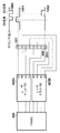
<画像形成装置の制御系>
図4は、図1に示す画像形成装置100で用いられる制御系の一例を説明するための制御ブロック図である。なお、光走査装置104Y、104M、104C、及び104Bkの構成は同一であるので、以下の説明では添え字Y、M、C、Bkを省略する。なお、図4では、8ビームに関する構成を、並列繰返しであるので一部省略して示している。
<Control system of image forming apparatus>
FIG. 4 is a control block diagram for explaining an example of a control system used in the
画像形成装置100は、CPU401、画像コントローラ402、光走査装置104、感光ドラム102、水晶発振器407、CPUバス404、及び光走査装置104内に配置されたEEPROM410を備える。CPU401及び画像コントローラ402は、画像形成装置本体に備えられており、その両方とも各光走査装置104に接続されている。光走査装置104は、PWMIC406と、第1及び第2のレーザドライバ(レーザドライバIC)405A及び405Bとを有している。なお、説明を簡易にするために、図4には、Y、M、C、Bkのうちの1色に対応する第1及び第2のレーザドライバ405A及び405B、並びに発光点301〜308(発光素子)を記載している。実際には、Y、M、C、Bkの各色に対して第1及び第2のレーザドライバ405A及び405B、並びに発光点301〜308が設けられている。
The
CPU401は、各光走査装置104を含む画像形成装置全体を制御する。CPU401は、水晶発振器407から100MHzの基準クロックの供給を受ける。CPU401は、内蔵されたPLL回路により基準クロックを10逓倍することによって、レーザ走査系の画像クロックである1GHzのクロックを生成する。なお、CPU401は、光走査装置104内に備えられていてもよい。その場合、CPU401は、画像形成装置本体に備えられた、画像形成装置全体を制御するCPU(図示せず)からの指示に従って、光走査装置104の動作を制御する。
The
画像コントローラ402は、画像形成装置100に接続された外部装置あるいは画像形成装置に取付られた読取装置から受信した画像データをY、M、C、Bkの4色の色成分に分離する。画像コントローラ402は、基準クロックに同期して、Y、M、C、Bkの4色の色成分の画像データをCPUバス404を介してCPU401に出力する。
The
CPU401は、画像コントローラ402から受け取った画像データをメモリ(図示せず)に格納し、メモリに格納した画像データを画像クロックに基づいて差動信号(LVDS:Low Differential Voltage Signal)に変換する。CPU401は、BD信号と画像クロック信号とに基づくタイミングで差動信号を、CPUバス404を介してPWMIC406に出力する。
The
PWMIC406は、CPU401から入力された差動信号に基づいて、各発光点301〜308から出射されるレーザ光のPWM変調に用いられるPWM信号を生成し、レーザドライバ405A及び405Bに供給する。なお、PWMIC406は、各レーザドライバに対して、当該レーザドライバが駆動対象としている発光点に対応するPWM信号を供給する。即ち、PWMIC406は、レーザドライバ405Aが駆動対象としている発光点に対応するPWM信号をレーザドライバ405Aに供給し、レーザドライバ405Bが駆動対象としている発光点に対応するPWM信号をレーザドライバ405Bに供給する。
The
本実施例の光走査装置104は、複数の駆動ICの一例として、レーザドライバ405A及び405Bを備える。レーザドライバ405A及び405Bは、それぞれが発光点301〜308のうちの1つ以上の発光点に駆動電流を供給する。レーザドライバ405A及び405Bは、それぞれが異なる発光点を駆動対象としている。具体的には、図4に示すように、レーザドライバ405Aは、発光点301〜304を駆動対象とし、レーザドライバ405Bは、発光点305〜308を駆動対象としている。
The
本実施例のレーザドライバ405A及び405Bは、同じ部品型番の集積回路(IC)で構成されたレーザ駆動IC(レーザドライバIC)であり、それぞれ発光点301〜304及び発光点305〜308を制御する。レーザドライバ405A及び405Bには、本体背面基板(図示せず)から直流5V線とグランド線が供給されており、レーザドライバ405A及び405B並びに発光点301〜308には共通の電源から電力が供給される。
The
レーザドライバ405A及び405Bは、駆動対象とする発光点に対して、PWMIC406から供給されるPWM信号に基づく駆動電流を供給することで、静電潜像を形成するためのレーザ光を各発光点から出射させる。また、レーザドライバ405A及び405Bは、CPU401からの指示に従って、駆動対象(制御対象)とする発光点に対する自動光量制御(APC:Automatic Power Control)を実行する。EEPROM410には、光走査装置104において実行すべきAPCシーケンスに関する情報が記憶されている。CPU401は、EEPROM410に記憶されているAPCシーケンスに関する情報に基づく順序で各発光点に対するAPCを実行するよう、レーザドライバ405A及び405Bを制御する。
The
レーザドライバ405A及び405Bは、駆動対象とする発光点のうちの1つに対するAPCを実行する場合、PD204によって検出されるレーザ光の光量に応じて当該発光点に供給する駆動電流の値を制御する。これにより、レーザドライバ405A及び405Bは、当該発光点から出射されるレーザ光の光量を目標光量に制御する。なお、PD204は、発光点301〜308からそれぞれ出射されるレーザ光の光量を検出する光量検出手段の一例である。CPU401は、後述するように、レーザ光の1走査周期ごとに、APCの実行対象とする発光点を、1走査周期内でAPCを実行可能な発光点の数に応じて順次切り替えながら、各発光点に対してAPCを順に実行する。
When the
<BD間隔測定>
画像形成装置100では、図3(a)に示すような光源(半導体レーザ200)の構成に起因して、図3(b)に示すように、各発光点から出射されたレーザ光が、感光ドラム102上で主走査方向において異なる位置S1〜S8に結像する。この場合、各発光点から出射されるレーザ光によって形成される静電潜像(画像)の主走査方向の書き出し位置を一定とするために、レーザ光を出射するタイミングを発光点ごとに適切に制御する必要がある。
<BD interval measurement>
In the
本実施例では、CPU401は、N個(本実施例では、N=8)の発光点のうち2つの発光点(第1及び第2の発光点)が2つのレーザ光(第1及び第2の光ビーム)を順に出射するよう、レーザドライバ405A及び405Bを制御する。更に、CPU401は、2つのレーザ光がBDセンサ210に順に入射することによってBDセンサ210によって順に生成される、2つのレーザ光に対応する2つのBD信号(第1及び第2の検出信号)の時間間隔(本明細書では「BD間隔」とも称する。)を測定する(BD間隔測定)。CPU401は、このBD間隔測定を、記録媒体への画像形成を行わない非画像形成期間に行う。更に、CPU401は、画像形成を行う画像形成期間には、レーザ光の1走査周期ごとに生成される単一のBD信号を基準として、各発光点の、画像データに基づくレーザ光の相対的な出射タイミングを、BD間隔測定によって得られた測定値に基づいて制御する。
In the present embodiment, the
BD間隔測定では、測定誤差を低減するためには、上述のように、測定に用いる第1及び第2の発光点からのレーザ光(第1及び第2の光ビーム)がBDセンサ210へ入射する際の光量を一定にする必要がある。BDセンサ210へ入射するレーザ光の光量は、測定に用いる第1及び第2の発光点に対してAPCを実行することによって、一定の光量(目標光量)に制御することが可能である。しかし、上述のように、第1及び第2の発光点を駆動するタイミングにおけるレーザドライバIC(レーザドライバ405A及び405B)の温度に起因して、第1及び2の発光点にそれぞれ供給する駆動電流の大きさにばらつきが生じうる。BD間隔測定の際に第1及び第2の発光点に供給する駆動電流の大きさにばらつきがあると、BD間隔測定の精度が劣化しうる。
In the BD interval measurement, in order to reduce the measurement error, the laser light (first and second light beams) from the first and second light emitting points used for measurement is incident on the
<本実施例の概要>
ここで、図5は、画像形成装置100における画像形成の実行時の、レーザドライバIC(レーザドライバ405A)の温度変化の一例を示す図であり、約24秒間に12枚のA4用紙に対する画像形成を連続して実行した例を示している。図5に示すように、画像形成の開始前に27℃であったレーザドライバ405Aは、画像形成が開始されると40℃程度まで上昇する。その後、レーザドライバ405Aは、用紙への画像形成時(約1秒間)の発熱と、紙間の非画像形成時(約1秒間)の放熱とを繰り返すことにより、その温度が上昇と低下とを繰り返す。画像形成が終了すると、レーザドライバ405Aは、時間とともに放熱し、その温度は緩やかに低下する。
<Outline of the present embodiment>
Here, FIG. 5 is a diagram illustrating an example of a temperature change of the laser driver IC (
次に、図6は、上述のような温度特性を有するレーザドライバIC(レーザドライバ405A)を用いてBD間隔測定を実行する場合の、レーザドライバICの温度変化の一例を示す図である。図6は、BDセンサ210の出力信号600と、発光点301及び304(LD1及びLD4)の光量601及び604と、レーザドライバ405A内の、駆動対象としている発光点301〜304に対応する駆動回路の局所的な温度620とを示している。
Next, FIG. 6 is a diagram illustrating an example of a temperature change of the laser driver IC when the BD interval measurement is performed using the laser driver IC (
図6は、LD1及びLD4が、BD間隔測定における第1及び第2の発光点として用いられる例を示している。まず、レーザドライバ405Aは、BDセンサ210に第1のBD信号を生成させるために、LD1を5μs間点灯させる。レーザドライバ405Aは、LD1を消灯させてから2μs後に、BDセンサ210に第2のBD信号を生成させるために、LD4を5μs間点灯させる。これにより、図6に示すように、第1及び第2のBD信号がBDセンサ210によって生成及び出力される。CPU401は、第1及びBD信号の時間間隔を、例えば各BD信号の立下りを基準として測定し、その測定結果は7μs程度となる。
FIG. 6 shows an example in which LD 1 and LD 4 are used as the first and second light emitting points in the BD interval measurement. First, the
BD間隔測定の実行中の、レーザドライバ405A内の駆動回路の温度620は、LD1及びLD4の発光に伴って上昇及び低下している。特に、第1のBD信号の生成タイミング(立下りのタイミング)よりも、第2のBD信号の生成タイミング(立下りのタイミング)の方が、温度620が14℃程度高くなっている。これは、LD1の発光に伴う発熱及び放熱に対応する温度成分611と、LD 4 の発光に伴う発熱及び放熱に対応する温度成分612とに依存している。即ち、LD1を消灯してから、駆動回路の温度が十分に低下する前に、LD 4 の発光を開始することによって、第1のBD信号の生成タイミングよりも第2のBD信号の生成タイミングの方が、駆動回路の温度620が高くなる。なお、温度成分611及び612の変化は、ICのグランドまたは電源電極層を介した内部熱拡散の、比較的短い(数μsの)時定数と、ICの端子を介した外部熱拡散の、比較的長い(数10msの)時定数と、IC内部の寄生抵抗の温度特性とに依存している。
During the BD interval measurement, the
図6に示すような駆動回路の温度620の変化に起因して、BD間隔測定において第1の発光点に供給する駆動電流よりも、第2の発光点に供給する駆動電流が減少する。これにより、BD間隔の測定値が、同一の大きさの駆動電流を第1及び第2の発光点に供給した場合よりも大きな値に変化してしまい、上述のように、BD間隔の測定精度が劣化することになる。しかし、このようなBD間隔の測定精度を劣化を防ぐためには、BD間隔の測定に用いる第1及び第2の発光点へ供給する駆動電流をできるだけ一定にする必要がある。
Due to the change in the
そこで、本実施例の画像形成装置100は、BD間隔測定に用いる第1及び第2の発光点として、異なるレーザドライバICによる駆動対象となっている2つの発光点を用いる。即ち、画像形成装置100のCPU401は、異なるレーザドライバICによる駆動対象となっている第1及び第2の発光点が第1及び第2のレーザ光を順に出射するよう、当該第1及び第2の発光点のそれぞれを駆動対象とするレーザドライバICを制御する。更に、CPU401は、第1及び第2のレーザ光が入射することによってBDセンサ210によって生成される、第1及び第2のレーザ光に対応する2つのBD信号の時間間隔を測定する。具体的には、画像形成装置100は、レーザドライバ405Aによる駆動対象となっている発光点301(LD1)を、第1の発光点として用い、レーザドライバ405Bによる駆動対象となっている発光点308(LD8)を、第2の発光点として用いる。
Therefore, the
このようにして、CPU401は、レーザドライバ405A及び405B内の、発光点301及び308に対応する駆動回路の温度がレーザドライバ間で同様に変化するように、レーザドライバ405A及び405Bを制御する。これにより、BD間隔測定の際に第1及び第2の発光の発光点に供給される駆動電流を同じ大きさとし、BD間隔の測定精度の劣化を抑えることが可能になる。
In this manner, the
<BD間隔測定の実行例>
次に、図7は、第1の実施例に係る、BD間隔測定に関連する光走査装置104の構成例を示す図である。本実施例では、レーザドライバ405Aは、半導体レーザ200の発光点301〜304に接続され、それらの発光点を駆動対象としている。また、レーザドライバ405Bは、半導体レーザ200の発光点305〜308に接続され、それらの発光点を駆動対象としている。BD間隔測定には、異なるレーザドライバIC(レーザドライバ405A及び405B)による駆動対象となっている発光点301及び308(LD1及びLD8)が、第1及び第2の発光点として用いられる。なお、これらのLD1及びLD8は、図7に示すように、半導体レーザ200内で直線状に一列に配置された発光点301〜308のうち、一端及び他端に配置されている発光点である。
<Execution example of BD interval measurement>
Next, FIG. 7 is a diagram illustrating a configuration example of the
具体的には、CPU401は、LD1及びLD8が、図7(LD1及びLD8の光量701及び708)に示すように、順にレーザ光を出射するように、レーザドライバ405A及び405Bを制御する。レーザドライバ405A及び405Bはそれぞれ、例えば事前に実行されるAPCによって定まる、同じ大きさの駆動電流を、異なるタイミングにLD1及びLD8に対して供給する。これにより、LD1及びLD8から出射されたレーザ光がBDセンサ210に順に入射し、BDセンサ210の出力信号700として、2つのBD信号(第1及び第2のBD信号)が生成される。
Specifically,
ここで、図8は、画像形成装置100における画像形成の実行時の、レーザドライバ405A及び405Bの温度変化の一例を示す図であり、約24秒間に12枚のA4用紙に対する画像形成を連続して実行した例を示している。なお、図8は、レーザドライバ405A及び405B全体の平均温度801及び802と、平均温度801及び802の温度差803とを示している。画像形成の開始前に27℃であったレーザドライバ405A及び405Bは、画像形成が開始されると40℃程度まで上昇する。その後、レーザドライバ405A及び405Bは、用紙への画像形成時(約1秒間)の発熱と、紙間の非画像形成時(約1秒間)の放熱とを繰り返すことにより、その温度が上昇と低下とを繰り返す。画像形成が終了すると、レーザドライバ405A及び405Bは、時間とともに放熱し、その温度は緩やかに低下する。
Here, FIG. 8 is a diagram illustrating an example of a temperature change of the
図8に示すように、レーザドライバ405A及び405B全体の平均温度801及び802の温度差803は、全体として約2.5℃以下となっており、概ね同様の温度変化を示している。このため、複数の用紙に連続的に画像形成を実行している間に、紙間にBD間隔測定を実行する場合の、レーザドライバ405A及び405Bの温度差がBD間隔測定の精度に与える影響は、比較的小さいといえる。
As shown in FIG. 8, the
次に、図9は、BD間隔測定を実行する場合の、レーザドライバ405A及び405Bの温度変化の一例を示す図である。図9は、BDセンサ210の出力信号900と、発光点301及び308(LD1及びLD8)の光量901及び908と、レーザドライバ405A及び405B内の、発光点301及び308に対応する駆動回路の局所的な温度911及び918とを示している。
Next, FIG. 9 is a diagram illustrating an example of a temperature change of the
図9に示すように、BD間隔測定の実行時には、LD1及びLD8の発光に伴って、各駆動回路の温度は、短時間に10℃程度変化(上昇及び低下)する傾向にある。しかし、本実施例では、LD1の発光に伴う、レーザドライバ405A内の駆動回路の温度変化と、LD8の発光に伴う、レーザドライバ405B内の駆動回路の温度変化とが、互いに影響を及ぼすことがない。即ち、第1の発光点(LD1)に駆動電流を供給する際のレーザドライバ405A内の駆動回路の温度と、第2の発光点(LD8)に駆動電流を供給する際のレーザドライバ405A内の駆動回路の温度とが、図9に示すように同等の温度となる。
As shown in FIG. 9, when the BD interval measurement is performed, the temperature of each drive circuit tends to change (rise and fall) by about 10 ° C. in a short time with the light emission of LD 1 and LD 8 . However, in this embodiment, the temperature change of the drive circuit in the
以上説明したように、本実施例では、BD間隔測定に用いる第1及び第2の発光点として、異なるレーザドライバICである、レーザドライバ405A及び405Bによる駆動対象となっている2つの発光点301及び308を用いる。これにより、BD間隔測定の際に第1及び第2の発光の発光点に供給される駆動電流が、各発光点を駆動する駆動回路の温度変化に起因して異なる大きさとなることを防止でき、BD間隔の測定精度の劣化を抑えることが可能になる。
As described above, in this embodiment, as the first and second light emitting points used for the BD interval measurement, the two light emitting
[第2の実施例]
第1の実施例で説明した、BD間隔測定に用いる発光点301及び308(LD1及びLD8)に対応する、レーザドライバ405A及び405B内の駆動回路の温度特性は、各レーザドライバICの回路基板における駆動回路の配置に依存する傾向がある。したがって、発光点301及び308に対応する駆動回路の温度特性の一致度をより高めるためには、各レーザドライバICの構成を同一とし、かつ、各レーザドライバICの回路基板における駆動回路の配置を対称(同等)とすることが有益である。
[Second Embodiment]
The temperature characteristics of the drive circuits in the
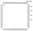
図10は、第2の実施例に係る、BD間隔測定に関連する光走査装置104の構成例を示す図である。本実施例では、レーザドライバ405A及び405Bは、同一の構成のICであり、図11に示すようなQFP(Quad Flat Package)パッケージで構成される。レーザドライバ405A及び405Bは、駆動対象とする1つ以上の発光点に対応する、それぞれ異なる発光点に駆動電流を供給する1つ以上の駆動回路を含んでいる。
FIG. 10 is a diagram illustrating a configuration example of the
具体的には、レーザドライバ405Aの番号47、44、41及び38の端子(端子1147、1144、1141及び1138)は、半導体レーザ200の発光点301、303、305及び307とそれぞれ接続されている。また、レーザドライバ405Bの番号47、44、41及び38の端子(端子1147、1144、1141及び1138)は、半導体レーザ200の発光点302、304、306及び308とそれぞれ接続されている。このような接続関係により、レーザドライバ405Aは、発光点301、303、305及び307を駆動対象としており、レーザドライバ405Bは、発光点302、304、306及び308を駆動対象としている。
Specifically, the
本実施例では、BD間隔測定に用いる発光点301及び308(LD1及びLD8)に対応する駆動回路は、異なるIC(レーザドライバ405A及び405B)の回路基板において同一の領域に配置される。具体的には、図10及び図11に示すように、LD1及びLD8に対応する駆動回路は、異なるIC(レーザドライバ405A及び405B)の回路基板における同一の端子1147を介して、LD1及びLD8とそれぞれ接続されている。これにより、レーザドライバICの回路基板における駆動回路の配置を対称とし、BD間隔測定の実行時におけるLD1及びLD8に対応する駆動回路の温度特性の一致度をより高めることが可能である。
In this embodiment, the drive circuits corresponding to the light emission points 301 and 308 (LD 1 and LD 8 ) used for the BD interval measurement are arranged in the same region in the circuit boards of different ICs (
[第3の実施例]
第2の実施例では、BD間隔測定の実行時における発光点301及び308(LD1及びLD8)に対応する駆動回路の温度特性の一致度をより高めるために、レーザドライバ405A及び405Bの回路基板における、各駆動回路の配置を対称としている。第3の実施例では、LD1及びLD8に対応する駆動回路の温度特性の一致度を第2の実施例よりも更に高めるために、レーザドライバ405A及び405Bによる、駆動対象としている各発光点に対するAPCの実行の対称性も考慮する。なお、光走査装置104の構成は、第2の実施例(図10及び図11)と同様である。
[Third embodiment]
In the second embodiment, the circuits of the
図12(a)は、第3の実施例に係る、光走査装置104の動作のタイミングを示すタイミングチャートである。図12(a)では、BDセンサ210の出力信号1201と、半導体レーザ200の発光状態1202とを示している。半導体レーザ200の各発光点(LD1〜LD8)から出射されるレーザ光の1走査周期は、感光ドラム102の画像領域を走査する画像形成期間と、画像領域以外の領域を走査する非画像形成期間とを含む。CPU401は、レーザ光の1走査周期ごとに、図12(a)に示すように、非画像形成期間を利用して各発光点に対するAPCを実行する。
FIG. 12A is a timing chart showing the operation timing of the
具体的には、CPU401は、レーザ光の1走査周期ごとに、複数のレーザドライバIC(レーザドライバ405A及び405B)のそれぞれに、駆動対象とする1つ以上の発光点のうちの同一の数の発光点に対してAPCを実行させる。更に、CPU401は、APCの実行後、次の画像形成期間の前に、BD間隔測定を実行する。このようにして、レーザ光の1走査周期ごとの各レーザドライバICによるAPCの実行に、対称性を与える。これにより、LD1及びLD8に対応する駆動回路の温度特性の一致度を更に高め、BD間隔の測定精度を向上させることが可能である。
Specifically, the
また、図12(a)に示すように、レーザ光の1走査周期ごとに、LD1及びLD8、LD3及びLD6、LD5及びLD4の順に、レーザドライバ405A及び405BがAPCを実行してもよい。即ち、レーザ光の1走査周期ごとに、レーザドライバ405A及び405Bにおける同一の端子(図10及び図11)に接続された発光点に対するAPCを実行している。このようなAPCの実行を制御することで、LD1及びLD8に対応する駆動回路の温度特性の一致度を更に高め、BD間隔の測定精度を更に向上させることが可能である。
Further, as shown in FIG. 12A, the
なお、図12(a)に示すように、APCの実行後、BD間隔測定が開始される直前に、所定の期間(期間1203)、発光点301〜308の全てを強制的に非発光状態にするよう、レーザドライバ405A及び405Bが制御されてもよい。所定の期間は、発光点301〜308に対応する駆動回路の温度を十分に低下させるための期間として設定され、例えば30μs以上に設定される。これにより、BD間隔測定の実行タイミングにおいて、発光点301〜308の温度を一様に低下させることができる。その結果、発光点301及び308(LD1及びLD8)に対応する駆動回路の温度特性の一致度を更に高め、BD間隔の測定精度を更に向上させることが可能である。
As shown in FIG. 12A, after the APC is executed, immediately before the BD interval measurement is started, all the
[第4の実施例]
第3の実施例では、図12(a)に示すように、APCの実行後、BD間隔測定が開始される直前に、所定の期間、発光点301〜308の全てを強制的に非発光状態にするよう、レーザドライバ405A及び405Bが制御する例を説明している。第4の実施例では、このような制御の変形例を説明する。
[Fourth embodiment]
In the third embodiment, as shown in FIG. 12 (a), after the APC is executed, immediately before the BD interval measurement is started, all the
図12(b)は、第4の実施例に係る、光走査装置104の動作のタイミングを示すタイミングチャートである。図12(b)に示すように、本実施例では、APCの実行後、BD間隔測定が開始される直前に、所定の期間(期間1213)、発光点301〜308の全てを強制的に発光状態にするよう、レーザドライバ405A及び405Bが制御される。所定の期間は、発光点301〜308に対応する駆動回路の温度が飽和状態となるのに十分な期間として設定され、例えば30μs以上に設定される。これにより、BD間隔測定の実行タイミングにおいて、発光点301〜308の温度を一様に飽和させることができる。その結果、発光点301及び308(LD1及びLD8)に対応する駆動回路の温度特性の一致度を更に高め、BD間隔の測定精度を更に向上させることが可能である。
FIG. 12B is a timing chart showing the operation timing of the
なお、上述の各実施例は、光走査装置104が2つのレーザドライバIC(レーザドライバ405A及び405B)を備える場合のみに限定されず、3つ以上のレーザドライバICを備える場合にも同様に適用できる。例えば、図13に示すように、光走査装置104は、4つのレーザドライバIC(レーザドライバ405A、405B、405C及び405D)を備えていてもよい。このような場合にも、上述の各実施例を同様に適用できる。
Each of the above-described embodiments is not limited to the case where the
100:画像形成装置、102(Y,M,C,K):感光ドラム、104(Y,M,C,K):光走査装置、200:半導体レーザ、301〜308(LD1〜LD8):発光点、205:ポリゴンミラー、210:BDセンサ、401:CPU、405A,405B:レーザドライバ 100: Image forming apparatus, 102 (Y, M, C , K): a photosensitive drum, 104 (Y, M, C , K): the optical scanning apparatus, 200: semiconductor laser, 301~308 (LD 1 ~LD 8) : Luminous point, 205: polygon mirror, 210: BD sensor, 401: CPU, 405A, 405B: laser driver
Claims (12)
前記複数の発光点から出射された複数のレーザ光が前記感光体を走査するよう、当該複数のレーザ光を偏向する偏向手段と、
前記偏向手段によって偏向されたレーザ光が入射する位置に設けられ、前記偏向手段によって偏向されたレーザ光が入射すると当該レーザ光を検出したことを示す検出信号を生成するビーム検出手段と、
それぞれが前記複数の発光点のうちの2つ以上の発光点に駆動電流を供給する複数のレーザドライバICであって、それぞれが異なる発光点を駆動対象とする、前記複数のレーザドライバICと、
前記複数の発光点のうちで、異なるレーザドライバICによる駆動対象となっている第1及び第2の発光点が第1及び第2のレーザ光を順に出射するよう、前記第1及び第2の発光点をそれぞれ駆動対象とする第1及び第2のレーザドライバICを制御し、前記ビーム検出手段によって生成される、前記第1及び第2のレーザ光に対応する2つの検出信号の時間間隔を測定する測定手段と、
前記測定手段によって測定された前記時間間隔に基づいて、前記複数の発光点のそれぞれの、画像データに基づくレーザ光の相対的な出射タイミングを制御する制御手段と、
を備えることを特徴とする画像形成装置。 A light source comprising a plurality of light emitting points each emitting laser light for exposing the photoreceptor;
So that a plurality of laser beams emitted from the plurality of light emitting points to scan the photosensitive member, and deflecting means for deflecting the plurality of laser beams,
The laser beam deflected by the deflecting means is provided at a position where the incident, the beam detection means laser beam deflected by said deflecting means for generating a detection signal indicating the detection of the laser beam made incident,
Each of which a plurality of the laser driver IC supplies a driving current to two or more light emitting points of the plurality of light emitting points, respectively different light emitting points to be driven, and the plurality of laser driver IC,
Among the plurality of light emitting points, different to the first and second light emitting point which is the driven by the laser driver IC emits a first and a second laser beam in order, the first and second The first and second laser driver ICs whose emission points are driven are controlled, and the time intervals between the two detection signals corresponding to the first and second laser beams generated by the beam detection unit are set. Measuring means for measuring;
Control means for controlling the relative emission timing of the laser light based on the image data of each of the plurality of light emitting points based on the time interval measured by the measuring means;
An image forming apparatus comprising:
前記第1及び第2の発光点にそれぞれ対応する駆動回路は、異なるレーザドライバICの回路基板において同一の領域に配置されている
ことを特徴とする請求項1に記載の画像形成装置。 Wherein the plurality of laser driver IC corresponds to two or more light emitting points to be driven, comprising two or more drive circuits for supplying a drive current to different emission points, an integrated circuit of the same configuration,
2. The image forming apparatus according to claim 1, wherein the drive circuits corresponding to the first and second light emission points are arranged in the same region on circuit boards of different laser driver ICs .
前記光量検出手段によって検出される光量に応じて駆動電流の値を制御することで発光点から出射されるレーザ光の光量を目標光量に制御する光量制御を実行するよう、前記複数のレーザドライバICを制御する光量制御手段と、を更に備え、
前記複数のレーザ光の1走査周期ごとに、
前記光量制御手段は、前記複数のレーザドライバICのそれぞれに、駆動対象とする2つ以上の発光点のうちの同一の数の発光点に対して前記光量制御を実行させ、
前記測定手段は、前記時間間隔の測定を実行する
を特徴とする請求項1に記載の画像形成装置。 A light amount detecting means for detecting a light amount of laser light respectively emitted from the plurality of light emitting points;
The plurality of laser driver ICs so as to execute light amount control for controlling the light amount of the laser light emitted from the light emitting point to the target light amount by controlling the value of the drive current according to the light amount detected by the light amount detecting means. A light amount control means for controlling
For each scanning period of the plurality of laser beams ,
The light quantity control means to each of the plurality of laser driver IC, to execute the light quantity control for the same number of light emitting points of the two or more light emitting points to be driven,
The image forming apparatus according to claim 1, wherein the measurement unit performs the measurement of the time interval.
前記第1及び第2の発光点にそれぞれ対応する駆動回路は、異なるレーザドライバICの回路基板において同一の領域に配置されている
ことを特徴とする請求項4に記載の画像形成装置。 Wherein the plurality of laser driver IC corresponds to two or more light emitting points to be driven, comprising two or more drive circuits for supplying a drive current to different emission points, an integrated circuit of the same configuration,
5. The image forming apparatus according to claim 4, wherein the drive circuits corresponding to the first and second light emitting points are arranged in the same region on circuit boards of different laser driver ICs .
ことを特徴とする請求項5または6に記載の画像形成装置。 The light quantity control means, wherein for each scanning period, to perform the light amount control with respect to the light emitting points corresponding to the drive circuits arranged in the same area in the circuit board of different laser driver IC, wherein the plurality of laser drivers The image forming apparatus according to claim 5, wherein an IC is controlled.
前記第1及び第2の発光点はそれぞれ、前記複数の発光点のうち一端及び他端に配置された発光点である
ことを特徴とする請求項1から9のいずれか1項に記載の画像形成装置。 The light emitting points are arranged in a straight line in the light source,
The image according to any one of claims 1 to 9, wherein the first and second light emitting points are light emitting points arranged at one end and the other end of the plurality of light emitting points, respectively. Forming equipment.
前記感光体を帯電させる帯電手段と、
前記複数のレーザ光による露光によって前記感光体に形成された静電潜像を現像して、記録媒体に転写すべき画像を前記感光体に形成する現像手段と、
を更に備えることを特徴とする請求項1から11のいずれか1項に記載の画像形成装置。 The photoreceptor;
Charging means for charging the photoreceptor;
Developing means for developing an electrostatic latent image formed on the photoconductor by exposure with the plurality of laser beams to form an image on the photoconductor to be transferred to a recording medium;
The image forming apparatus according to claim 1, further comprising:
Priority Applications (2)
| Application Number | Priority Date | Filing Date | Title |
|---|---|---|---|
| JP2014077259A JP6317610B2 (en) | 2014-04-03 | 2014-04-03 | Image forming apparatus |
| US14/675,993 US9575432B2 (en) | 2014-04-03 | 2015-04-01 | Image forming apparatus |
Applications Claiming Priority (1)
| Application Number | Priority Date | Filing Date | Title |
|---|---|---|---|
| JP2014077259A JP6317610B2 (en) | 2014-04-03 | 2014-04-03 | Image forming apparatus |
Publications (3)
| Publication Number | Publication Date |
|---|---|
| JP2015197669A JP2015197669A (en) | 2015-11-09 |
| JP2015197669A5 JP2015197669A5 (en) | 2017-04-27 |
| JP6317610B2 true JP6317610B2 (en) | 2018-04-25 |
Family
ID=54209682
Family Applications (1)
| Application Number | Title | Priority Date | Filing Date |
|---|---|---|---|
| JP2014077259A Active JP6317610B2 (en) | 2014-04-03 | 2014-04-03 | Image forming apparatus |
Country Status (2)
| Country | Link |
|---|---|
| US (1) | US9575432B2 (en) |
| JP (1) | JP6317610B2 (en) |
Families Citing this family (4)
| Publication number | Priority date | Publication date | Assignee | Title |
|---|---|---|---|---|
| JP6784561B2 (en) * | 2015-11-20 | 2020-11-11 | キヤノン株式会社 | controller |
| US9983502B2 (en) * | 2015-11-20 | 2018-05-29 | Canon Kabushiki Kaisha | Controller |
| JP6467461B2 (en) * | 2017-05-29 | 2019-02-13 | キヤノン株式会社 | Image forming apparatus and exposure apparatus |
| CN114615397B (en) * | 2020-12-09 | 2023-06-30 | 华为技术有限公司 | TOF device and electronic equipment |
Family Cites Families (17)
| Publication number | Priority date | Publication date | Assignee | Title |
|---|---|---|---|---|
| JP3471060B2 (en) * | 1994-01-14 | 2003-11-25 | コニカミノルタホールディングス株式会社 | Synchronous signal generator for image forming apparatus |
| US5586055A (en) * | 1994-09-20 | 1996-12-17 | Eastman Kodak Company | Non-uniformity correction of an LED printhead |
| JP3298042B2 (en) * | 1995-09-14 | 2002-07-02 | コニカ株式会社 | Image forming apparatus and control method of image forming apparatus |
| JP2001024273A (en) * | 1999-05-06 | 2001-01-26 | Asahi Optical Co Ltd | Optical output control circuit of multibeam laser device |
| US6867794B2 (en) * | 2003-01-30 | 2005-03-15 | Hewlett-Packard Development Company, L.P. | Adjusting a scan line in a laser imaging device |
| JP4605692B2 (en) * | 2004-03-19 | 2011-01-05 | 株式会社リコー | Semiconductor laser modulation driving apparatus and image forming apparatus |
| JP5016853B2 (en) * | 2006-06-09 | 2012-09-05 | キヤノン株式会社 | Image forming apparatus and laser light quantity correction method |
| JP4769640B2 (en) * | 2006-06-09 | 2011-09-07 | キヤノン株式会社 | Light quantity control apparatus, exposure apparatus, image forming apparatus, and light quantity control method |
| JP2008089695A (en) | 2006-09-29 | 2008-04-17 | Canon Inc | Image forming apparatus |
| JP2009292075A (en) * | 2008-06-06 | 2009-12-17 | Ricoh Co Ltd | Photo-writing device and image forming apparatus |
| JP2011064765A (en) * | 2009-09-15 | 2011-03-31 | Konica Minolta Business Technologies Inc | Light beam scanning optical device |
| JP5792960B2 (en) | 2010-01-28 | 2015-10-14 | キヤノン株式会社 | Image forming apparatus |
| JP6029314B2 (en) | 2012-04-24 | 2016-11-24 | キヤノン株式会社 | Image forming apparatus |
| US9341977B2 (en) | 2012-04-24 | 2016-05-17 | Canon Kabushiki Kaisha | Light emission apparatus, optical scanning apparatus having light emission apparatus, and image forming apparatus |
| JP2013228609A (en) | 2012-04-26 | 2013-11-07 | Canon Inc | Image forming device |
| JP6029315B2 (en) | 2012-04-26 | 2016-11-24 | キヤノン株式会社 | Image forming apparatus |
| JP6315967B2 (en) | 2013-12-11 | 2018-04-25 | キヤノン株式会社 | Optical scanning device and image forming apparatus using the same |
-
2014
- 2014-04-03 JP JP2014077259A patent/JP6317610B2/en active Active
-
2015
- 2015-04-01 US US14/675,993 patent/US9575432B2/en active Active
Also Published As
| Publication number | Publication date |
|---|---|
| US20150286159A1 (en) | 2015-10-08 |
| JP2015197669A (en) | 2015-11-09 |
| US9575432B2 (en) | 2017-02-21 |
Similar Documents
| Publication | Publication Date | Title |
|---|---|---|
| US9091955B2 (en) | Image forming apparatus | |
| JP6029314B2 (en) | Image forming apparatus | |
| JP6317610B2 (en) | Image forming apparatus | |
| EP2841280B1 (en) | Light emission apparatus, optical scanning apparatus having light emission apparatus, and image forming apparatus | |
| JP6315967B2 (en) | Optical scanning device and image forming apparatus using the same | |
| JP5824850B2 (en) | Optical device and method for controlling optical device | |
| JP6378538B2 (en) | Image forming apparatus | |
| US7567268B2 (en) | Image forming apparatus and abnormality detecting method | |
| JP6366327B2 (en) | Image forming apparatus | |
| WO2014207799A1 (en) | Image forming device | |
| JP6302331B2 (en) | Image forming apparatus | |
| US10365599B2 (en) | Image forming apparatus with write start timing determination | |
| JP2012151336A (en) | Image forming apparatus | |
| JP6368120B2 (en) | Image forming apparatus | |
| JP5923966B2 (en) | Optical writing apparatus and image forming apparatus | |
| JP2006251242A (en) | Optical scanner, method of optical scanning and optical scanning program | |
| JP2020006540A (en) | Image formation apparatus | |
| JP5968049B2 (en) | Image forming apparatus | |
| JP5943691B2 (en) | Light emitting device, optical scanning device including the light emitting device, and image forming apparatus | |
| JP2003182141A (en) | Imaging apparatus | |
| JP6401482B2 (en) | Image forming apparatus | |
| JP2011069871A (en) | Light beam scanning optical apparatus | |
| JP2016107565A (en) | Image formation apparatus |
Legal Events
| Date | Code | Title | Description |
|---|---|---|---|
| A521 | Written amendment |
Free format text: JAPANESE INTERMEDIATE CODE: A523 Effective date: 20170324 |
|
| A621 | Written request for application examination |
Free format text: JAPANESE INTERMEDIATE CODE: A621 Effective date: 20170324 |
|
| A977 | Report on retrieval |
Free format text: JAPANESE INTERMEDIATE CODE: A971007 Effective date: 20171113 |
|
| A131 | Notification of reasons for refusal |
Free format text: JAPANESE INTERMEDIATE CODE: A131 Effective date: 20171120 |
|
| A521 | Written amendment |
Free format text: JAPANESE INTERMEDIATE CODE: A523 Effective date: 20180119 |
|
| TRDD | Decision of grant or rejection written | ||
| A01 | Written decision to grant a patent or to grant a registration (utility model) |
Free format text: JAPANESE INTERMEDIATE CODE: A01 Effective date: 20180302 |
|
| A61 | First payment of annual fees (during grant procedure) |
Free format text: JAPANESE INTERMEDIATE CODE: A61 Effective date: 20180330 |
|
| R151 | Written notification of patent or utility model registration |
Ref document number: 6317610 Country of ref document: JP Free format text: JAPANESE INTERMEDIATE CODE: R151 |