JP6292155B2 - Substrate processing apparatus, substrate processing method, and storage medium - Google Patents
Substrate processing apparatus, substrate processing method, and storage medium Download PDFInfo
- Publication number
- JP6292155B2 JP6292155B2 JP2015056467A JP2015056467A JP6292155B2 JP 6292155 B2 JP6292155 B2 JP 6292155B2 JP 2015056467 A JP2015056467 A JP 2015056467A JP 2015056467 A JP2015056467 A JP 2015056467A JP 6292155 B2 JP6292155 B2 JP 6292155B2
- Authority
- JP
- Japan
- Prior art keywords
- substrate
- block
- module
- processing
- transfer
- Prior art date
- Legal status (The legal status is an assumption and is not a legal conclusion. Google has not performed a legal analysis and makes no representation as to the accuracy of the status listed.)
- Active
Links
- 239000000758 substrate Substances 0.000 title claims description 155
- 238000012545 processing Methods 0.000 title claims description 144
- 238000003672 processing method Methods 0.000 title claims description 8
- 238000003860 storage Methods 0.000 title claims description 7
- 230000007246 mechanism Effects 0.000 claims description 143
- 230000007723 transport mechanism Effects 0.000 claims description 118
- 230000032258 transport Effects 0.000 claims description 42
- 238000000034 method Methods 0.000 claims description 15
- 239000007788 liquid Substances 0.000 claims description 5
- 238000004590 computer program Methods 0.000 claims description 3
- 235000012431 wafers Nutrition 0.000 description 211
- 238000000576 coating method Methods 0.000 description 83
- 239000011248 coating agent Substances 0.000 description 81
- 238000010438 heat treatment Methods 0.000 description 56
- 230000001681 protective effect Effects 0.000 description 33
- 238000004140 cleaning Methods 0.000 description 28
- 238000004929 transmission Raman spectroscopy Methods 0.000 description 26
- 230000002093 peripheral effect Effects 0.000 description 18
- 101100233693 Saccharomyces cerevisiae (strain ATCC 204508 / S288c) ITC1 gene Proteins 0.000 description 16
- 238000000072 solvent casting and particulate leaching Methods 0.000 description 14
- 101000679575 Homo sapiens Trafficking protein particle complex subunit 2 Proteins 0.000 description 12
- 102100022613 Trafficking protein particle complex subunit 2 Human genes 0.000 description 12
- 230000015572 biosynthetic process Effects 0.000 description 9
- 101100095173 Arabidopsis thaliana SCPL11 gene Proteins 0.000 description 6
- 101100095174 Arabidopsis thaliana SCPL12 gene Proteins 0.000 description 6
- 239000000126 substance Substances 0.000 description 6
- 101150075071 TRS1 gene Proteins 0.000 description 5
- 230000002209 hydrophobic effect Effects 0.000 description 5
- 239000002245 particle Substances 0.000 description 5
- 101100476845 Arabidopsis thaliana SCPL1 gene Proteins 0.000 description 4
- 238000005192 partition Methods 0.000 description 4
- 101100202554 Arabidopsis thaliana SCPL6 gene Proteins 0.000 description 3
- 101100476879 Arabidopsis thaliana SCPL2 gene Proteins 0.000 description 2
- 101100309661 Arabidopsis thaliana SCPL3 gene Proteins 0.000 description 2
- 101100202547 Arabidopsis thaliana SCPL4 gene Proteins 0.000 description 2
- 102100026437 Branched-chain-amino-acid aminotransferase, cytosolic Human genes 0.000 description 2
- 101000766268 Homo sapiens Branched-chain-amino-acid aminotransferase, cytosolic Proteins 0.000 description 2
- 101000662809 Homo sapiens Trafficking protein particle complex subunit 4 Proteins 0.000 description 2
- 101000662805 Homo sapiens Trafficking protein particle complex subunit 5 Proteins 0.000 description 2
- 101100500679 Neurospora crassa (strain ATCC 24698 / 74-OR23-1A / CBS 708.71 / DSM 1257 / FGSC 987) cot-3 gene Proteins 0.000 description 2
- 101100384866 Saccharomyces cerevisiae (strain ATCC 204508 / S288c) COT1 gene Proteins 0.000 description 2
- 102100037496 Trafficking protein particle complex subunit 4 Human genes 0.000 description 2
- 102100037497 Trafficking protein particle complex subunit 5 Human genes 0.000 description 2
- 210000000078 claw Anatomy 0.000 description 2
- 230000000694 effects Effects 0.000 description 2
- 238000007654 immersion Methods 0.000 description 2
- 239000004065 semiconductor Substances 0.000 description 2
- 239000007787 solid Substances 0.000 description 2
- 101100202553 Arabidopsis thaliana SCPL5 gene Proteins 0.000 description 1
- 102100026413 Branched-chain-amino-acid aminotransferase, mitochondrial Human genes 0.000 description 1
- 101000766294 Homo sapiens Branched-chain-amino-acid aminotransferase, mitochondrial Proteins 0.000 description 1
- 101100283849 Saccharomyces cerevisiae (strain ATCC 204508 / S288c) GRR1 gene Proteins 0.000 description 1
- NVEDPFICKAIHKD-NGYBGAFCSA-N chembl2086638 Chemical compound ClC1=CC(Cl)=CC(Cl)=C1OCC(=O)N\N=C\C1=CC=CN1 NVEDPFICKAIHKD-NGYBGAFCSA-N 0.000 description 1
- 239000000498 cooling water Substances 0.000 description 1
- 238000003384 imaging method Methods 0.000 description 1
- 230000002452 interceptive effect Effects 0.000 description 1
- 238000004519 manufacturing process Methods 0.000 description 1
- 239000003595 mist Substances 0.000 description 1
- 230000003287 optical effect Effects 0.000 description 1
- 238000000206 photolithography Methods 0.000 description 1
- 229920002120 photoresistant polymer Polymers 0.000 description 1
- 238000012805 post-processing Methods 0.000 description 1
- 230000000153 supplemental effect Effects 0.000 description 1
Images


Classifications
-
- H—ELECTRICITY
- H01—ELECTRIC ELEMENTS
- H01L—SEMICONDUCTOR DEVICES NOT COVERED BY CLASS H10
- H01L21/00—Processes or apparatus adapted for the manufacture or treatment of semiconductor or solid state devices or of parts thereof
- H01L21/67—Apparatus specially adapted for handling semiconductor or electric solid state devices during manufacture or treatment thereof; Apparatus specially adapted for handling wafers during manufacture or treatment of semiconductor or electric solid state devices or components ; Apparatus not specifically provided for elsewhere
- H01L21/67005—Apparatus not specifically provided for elsewhere
- H01L21/67011—Apparatus for manufacture or treatment
- H01L21/67155—Apparatus for manufacturing or treating in a plurality of work-stations
- H01L21/67196—Apparatus for manufacturing or treating in a plurality of work-stations characterized by the construction of the transfer chamber
-
- H—ELECTRICITY
- H01—ELECTRIC ELEMENTS
- H01L—SEMICONDUCTOR DEVICES NOT COVERED BY CLASS H10
- H01L21/00—Processes or apparatus adapted for the manufacture or treatment of semiconductor or solid state devices or of parts thereof
- H01L21/67—Apparatus specially adapted for handling semiconductor or electric solid state devices during manufacture or treatment thereof; Apparatus specially adapted for handling wafers during manufacture or treatment of semiconductor or electric solid state devices or components ; Apparatus not specifically provided for elsewhere
- H01L21/677—Apparatus specially adapted for handling semiconductor or electric solid state devices during manufacture or treatment thereof; Apparatus specially adapted for handling wafers during manufacture or treatment of semiconductor or electric solid state devices or components ; Apparatus not specifically provided for elsewhere for conveying, e.g. between different workstations
-
- G—PHYSICS
- G03—PHOTOGRAPHY; CINEMATOGRAPHY; ANALOGOUS TECHNIQUES USING WAVES OTHER THAN OPTICAL WAVES; ELECTROGRAPHY; HOLOGRAPHY
- G03F—PHOTOMECHANICAL PRODUCTION OF TEXTURED OR PATTERNED SURFACES, e.g. FOR PRINTING, FOR PROCESSING OF SEMICONDUCTOR DEVICES; MATERIALS THEREFOR; ORIGINALS THEREFOR; APPARATUS SPECIALLY ADAPTED THEREFOR
- G03F7/00—Photomechanical, e.g. photolithographic, production of textured or patterned surfaces, e.g. printing surfaces; Materials therefor, e.g. comprising photoresists; Apparatus specially adapted therefor
- G03F7/70—Microphotolithographic exposure; Apparatus therefor
- G03F7/70691—Handling of masks or workpieces
- G03F7/70733—Handling masks and workpieces, e.g. exchange of workpiece or mask, transport of workpiece or mask
- G03F7/7075—Handling workpieces outside exposure position, e.g. SMIF box
-
- H—ELECTRICITY
- H01—ELECTRIC ELEMENTS
- H01L—SEMICONDUCTOR DEVICES NOT COVERED BY CLASS H10
- H01L21/00—Processes or apparatus adapted for the manufacture or treatment of semiconductor or solid state devices or of parts thereof
- H01L21/02—Manufacture or treatment of semiconductor devices or of parts thereof
-
- H—ELECTRICITY
- H01—ELECTRIC ELEMENTS
- H01L—SEMICONDUCTOR DEVICES NOT COVERED BY CLASS H10
- H01L21/00—Processes or apparatus adapted for the manufacture or treatment of semiconductor or solid state devices or of parts thereof
- H01L21/67—Apparatus specially adapted for handling semiconductor or electric solid state devices during manufacture or treatment thereof; Apparatus specially adapted for handling wafers during manufacture or treatment of semiconductor or electric solid state devices or components ; Apparatus not specifically provided for elsewhere
- H01L21/67005—Apparatus not specifically provided for elsewhere
- H01L21/67011—Apparatus for manufacture or treatment
- H01L21/67155—Apparatus for manufacturing or treating in a plurality of work-stations
- H01L21/67161—Apparatus for manufacturing or treating in a plurality of work-stations characterized by the layout of the process chambers
- H01L21/67173—Apparatus for manufacturing or treating in a plurality of work-stations characterized by the layout of the process chambers in-line arrangement
-
- H—ELECTRICITY
- H01—ELECTRIC ELEMENTS
- H01L—SEMICONDUCTOR DEVICES NOT COVERED BY CLASS H10
- H01L21/00—Processes or apparatus adapted for the manufacture or treatment of semiconductor or solid state devices or of parts thereof
- H01L21/67—Apparatus specially adapted for handling semiconductor or electric solid state devices during manufacture or treatment thereof; Apparatus specially adapted for handling wafers during manufacture or treatment of semiconductor or electric solid state devices or components ; Apparatus not specifically provided for elsewhere
- H01L21/67005—Apparatus not specifically provided for elsewhere
- H01L21/67011—Apparatus for manufacture or treatment
- H01L21/67155—Apparatus for manufacturing or treating in a plurality of work-stations
- H01L21/67161—Apparatus for manufacturing or treating in a plurality of work-stations characterized by the layout of the process chambers
- H01L21/67178—Apparatus for manufacturing or treating in a plurality of work-stations characterized by the layout of the process chambers vertical arrangement
-
- H—ELECTRICITY
- H01—ELECTRIC ELEMENTS
- H01L—SEMICONDUCTOR DEVICES NOT COVERED BY CLASS H10
- H01L21/00—Processes or apparatus adapted for the manufacture or treatment of semiconductor or solid state devices or of parts thereof
- H01L21/67—Apparatus specially adapted for handling semiconductor or electric solid state devices during manufacture or treatment thereof; Apparatus specially adapted for handling wafers during manufacture or treatment of semiconductor or electric solid state devices or components ; Apparatus not specifically provided for elsewhere
- H01L21/677—Apparatus specially adapted for handling semiconductor or electric solid state devices during manufacture or treatment thereof; Apparatus specially adapted for handling wafers during manufacture or treatment of semiconductor or electric solid state devices or components ; Apparatus not specifically provided for elsewhere for conveying, e.g. between different workstations
- H01L21/67703—Apparatus specially adapted for handling semiconductor or electric solid state devices during manufacture or treatment thereof; Apparatus specially adapted for handling wafers during manufacture or treatment of semiconductor or electric solid state devices or components ; Apparatus not specifically provided for elsewhere for conveying, e.g. between different workstations between different workstations
Description
本発明は、基板を処理するための複数積層された処理モジュールを備える基板処理装置、基板処理方法及び記憶媒体に関する。 The present invention relates to a substrate processing apparatus including a plurality of stacked processing modules for processing a substrate, a substrate processing method, and a storage medium.
半導体デバイスの製造工程におけるフォトリソグラフィ工程においては、塗布、現像装置と、露光装置とが接続されて構成されるレジストパターン形成システムによって、基板である半導体ウエハ(以下、ウエハと記載する)にレジストパターンの形成が行われる。塗布、現像装置は、ウエハにレジスト膜を形成するためにレジストを塗布するレジスト塗布モジュール、露光装置により露光されたレジスト膜に現像液を供給してレジストパターンを形成する現像モジュール、ウエハに薬液を供給して露光装置による露光時にレジスト膜を保護するための保護膜を形成する保護膜形成モジュールなどの各種の薬液を供給する液処理モジュールを備える。また、塗布、現像装置には各液処理の前後でウエハを加熱処理する加熱モジュールも設けられる。特許文献1には、このような塗布、現像装置の例が記載されている。
In a photolithography process in the manufacturing process of a semiconductor device, a resist pattern is formed on a semiconductor wafer (hereinafter referred to as a wafer) as a substrate by a resist pattern forming system configured by connecting a coating / developing apparatus and an exposure apparatus. Is formed. The coating and developing apparatus includes a resist coating module for applying a resist to form a resist film on the wafer, a developing module for supplying a developing solution to the resist film exposed by the exposure apparatus to form a resist pattern, and a chemical solution to the wafer. A liquid processing module for supplying various chemicals such as a protective film forming module for supplying and forming a protective film for protecting the resist film during exposure by the exposure apparatus is provided. The coating and developing apparatus is also provided with a heating module that heats the wafer before and after each liquid treatment.
近年、露光装置のスループットが上昇しており、上記のレジストパターン形成システムの生産性を向上させるために、塗布、現像装置についてもスループットを向上させることが求められている。具体的には、例えば1時間あたり275枚程度のウエハを処理可能であるように塗布、現像装置を構成することが求められている。そのようにスループットを向上させるためには、塗布、現像装置において、ウエハに同じ種類の処理を行うモジュールの数を増やし、これらのモジュールで並行して処理を行うことが考えられる。 In recent years, the throughput of the exposure apparatus has increased, and in order to improve the productivity of the resist pattern forming system, it is required to improve the throughput of the coating and developing apparatus. Specifically, it is required to configure the coating and developing apparatus so that, for example, about 275 wafers per hour can be processed. In order to improve the throughput in this way, it is conceivable to increase the number of modules that perform the same type of processing on the wafer in the coating and developing apparatus, and perform processing in parallel with these modules.
例えば、上記の特許文献1では、上下に複数段に区画される単位ブロックを夫々備える前方側処理ブロック、後方側処理ブロックを露光装置に向かって横方向に配列した塗布、現像装置が示され、各単位ブロックには処理モジュール、加熱モジュール及びモジュール間でウエハを搬送する搬送機構を夫々備える。このような構成により、各種のモジュールの増設が図られている。上記の後方側処理ブロックでは、下段側の単位ブロックに保護膜形成モジュールが設けられ、上段側の単位ブロックに露光前にウエハの裏面を洗浄する裏面洗浄モジュールが設けられており、保護膜形成モジュール、裏面洗浄モジュール共にウエハを処理するためのカップが、前方側処理ブロック、後方側処理ブロックの配列方向に沿って2つ配置された構成とされている。
For example, in the above-mentioned
この特許文献1の塗布、現像装置では、露光装置にて処理された露光済みのウエハが後方側処理ブロックを通過して、前方側処理ブロックに搬送されて処理を受ける。上記のように後方側処理ブロックに保護膜形成モジュール及び裏面洗浄モジュールが設けられていると、後方側処理ブロックの各単位ブロックの搬送機構は、これらの各モジュールに対して露光前のウエハを搬送する合間に露光済みのウエハを搬送することになり、当該搬送機構の負荷が大きくなるので、スループットを十分に上昇させることができなくなる懸念がある。
In the coating and developing apparatus disclosed in
ところで、上記の裏面洗浄モジュールについては、後方側処理ブロックと露光装置とを互いに接続するインターフェイスブロックに設けてもよいとされ、そのように裏面洗浄モジュールをインターフェイスブロックに配置すると、後方側処理ブロックに設けられるカップの数に対して後段処理ブロックの専有床面積(フットプリント)が比較的大きい構成となる。塗布、現像装置においてはフットプリントを抑えつつ、モジュールの増設を図ることが求められる。つまり、この特許文献1に記載の塗布、現像装置よりさらにフットプリントを抑え、且つ高いスループットが得られる装置が求められている。
By the way, the back surface cleaning module described above may be provided in an interface block that connects the back side processing block and the exposure apparatus to each other. If the back surface cleaning module is arranged in the interface block as described above, The exclusive floor area (footprint) of the post-processing block is relatively large with respect to the number of cups provided. In the coating and developing apparatus, it is required to increase the number of modules while suppressing the footprint. That is, there is a demand for an apparatus that can further suppress the footprint and obtain a high throughput than the coating and developing apparatus described in
本発明はかかる点に鑑みてなされたものであり、本発明の課題は基板処理装置において、占有床面積を抑え、且つ高いスループットが得られる技術を提供することである。 This invention is made | formed in view of this point, and the subject of this invention is providing the technique which suppresses an occupied floor area and can obtain high throughput in a substrate processing apparatus.
本発明の基板処理装置は、キャリアに格納された基板を払い出すためのキャリアブロックと、当該キャリアブロックから払い出された基板を当該キャリアブロックに戻し、前記キャリアブロックに対して横方向に設けられるエンドブロックと、前記キャリアブロックと前記エンドブロックとの間に介在する中間ブロックと、を備える基板処理装置において、
前記中間ブロックは、
前記キャリアブロックから払い出されて前記エンドブロックに向かう前記基板、及び前記エンドブロックから前記キャリアブロックに戻される前記基板のうちの一方のみを各々処理するために、互いに積層されて設けられた複数の第1の処理モジュールと、
前記キャリアブロック及び前記エンドブロックのうちの一方から当該中間ブロックに搬送された前記基板を前記各第1の処理モジュールに搬送し、前記キャリアブロック及びエンドブロックのうちの他方に受け渡すために昇降する第1の基板搬送機構と、
前記キャリアブロック及び前記エンドブロックのうち他方から一方に前記第1の処理モジュールを素通りするように基板を搬送する、前記第1の基板搬送機構とは別体の第2の基板搬送機構と、
を備え、
前記キャリアブロックと前記エンドブロックとの間には処理ブロックが介在すると共に前記中間ブロック及び前記処理ブロックのうちの一方が前記キャリアブロック側に、他方が前記エンドブロック側に夫々設けられ、
前記処理ブロックは、上下に互いに区画されると共に、前記キャリアブロックと前記エンドブロックとの間で基板を搬送するための第3の基板搬送機構を夫々備えた複数の単位ブロックにより構成され、
前記各単位ブロックには、前記第3の基板搬送機構により搬送される前記第1の処理モジュールによる処理前あるいは処理後の基板を処理するための第2の処理モジュールが設けられ、
前記中間ブロックは、前記第1の基板搬送機構と前記第2の基板搬送機構と第3の基板搬送機構との間で基板を受け渡すために上下方向に配置される複数の載置モジュールにより構成される受け渡し部を備え、
前記第1の基板搬送機構は、前記複数の載置モジュール間で前記基板を搬送する載置モジュール間搬送機構を備え、
前記中間ブロックは、前記受け渡し部に対して側方から気体を供給する側方気体供給部と、前記側方気体供給部と共に前記受け渡し部を側方から挟むように前記載置モジュール間搬送機構に設けられた、前記気体を排気する側方排気部と、により構成される前記各載置モジュール間を横方向に流れる気流を形成する側方気流形成部を備える。
The substrate processing apparatus of the present invention returns a carrier block for paying out a substrate stored in a carrier and a substrate discharged from the carrier block to the carrier block, and is provided laterally with respect to the carrier block. In a substrate processing apparatus comprising an end block, and an intermediate block interposed between the carrier block and the end block,
The intermediate block is
In order to process only one of the substrate that is paid out from the carrier block and heads toward the end block, and the substrate that is returned from the end block to the carrier block, a plurality of layers are stacked on each other. A first processing module;
The substrate transported from one of the carrier block and the end block to the intermediate block is transported to the first processing module and moved up and down for delivery to the other of the carrier block and the end block. A first substrate transfer mechanism;
A second substrate transport mechanism separate from the first substrate transport mechanism, for transporting a substrate so as to pass through the first processing module from one of the carrier block and the end block to the other;
Bei to give a,
A processing block is interposed between the carrier block and the end block, and one of the intermediate block and the processing block is provided on the carrier block side, and the other is provided on the end block side.
The processing block is composed of a plurality of unit blocks each having a third substrate transport mechanism which is partitioned from each other vertically and transports a substrate between the carrier block and the end block.
Each unit block is provided with a second processing module for processing a substrate before or after processing by the first processing module transported by the third substrate transport mechanism,
The intermediate block includes a plurality of mounting modules arranged in the vertical direction to deliver a substrate between the first substrate transport mechanism, the second substrate transport mechanism, and the third substrate transport mechanism. Provided with a delivery part,
The first substrate transport mechanism includes a mounting module transport mechanism that transports the substrate between the plurality of mounting modules.
The intermediate block includes a side gas supply unit that supplies gas from the side to the transfer unit, and the inter-module transfer mechanism that sandwiches the transfer unit from the side together with the side gas supply unit. And a side airflow forming section that forms an airflow that flows in a lateral direction between the mounting modules .
本発明の基板処理方法は、 キャリアに格納された基板を払い出すためのキャリアブロックと、当該キャリアブロックから払い出された基板を当該キャリアブロックに戻し、前記キャリアブロックに対して横方向に設けられるエンドブロックと、前記キャリアブロックと前記エンドブロックとの間に介在する中間ブロックと、を備える基板処理装置を用いた基板処理方法において、
前記中間ブロックに設けられ、互いに積層されて設けられた複数の処理モジュールにて、前記キャリアブロックから払い出されて前記エンドブロックに向かう前記基板、及び前記エンドブロックから前記キャリアブロックに戻される前記基板のうちの一方のみを各々処理する工程と、
前記中間ブロックに設けられ、昇降可能な第1の基板搬送機構により、前記キャリアブロック及びエンドブロックのうちの一方から当該中間ブロックに搬送された前記基板を前記各処理モジュールに搬送し、前記キャリアブロック及びエンドブロックのうちの他方に受け渡す工程と、
前記中間ブロックに設けられる前記第1の基板搬送機構とは別体の第2の基板搬送機構により、前記キャリアブロック及びエンドブロックのうち他方から一方に前記処理モジュールを素通りするように基板を搬送する工程と、
を含み、
前記キャリアブロックと前記エンドブロックとの間には処理ブロックが介在すると共に前記中間ブロック及び前記処理ブロックのうちの一方が前記キャリアブロック側に、他方が前記エンドブロック側に夫々設けられ、
前記処理ブロックは、上下に互いに区画されると共に、前記キャリアブロックと前記エンドブロックとの間で基板を搬送するための第3の基板搬送機構を夫々備えた複数の単位ブロックにより構成され、
前記第3の基板搬送機構により搬送される前記第1の処理モジュールによる処理前あるいは処理後の基板を、前記各単位ブロックに設けられる第2の処理モジュールにより処理する工程と、
上下方向に配置される複数の載置モジュールにより構成されるように前記中間ブロックに設けられる受け渡し部を介して前記第1の基板搬送機構と前記第2の基板搬送機構と第3の基板搬送機構との間で基板を受け渡す工程と、
前記第1の基板搬送機構が備える載置モジュール間搬送機構により、前記複数の載置モジュール間で前記基板を搬送する工程と、
前記中間ブロックに設けられる側方気体供給部により、前記受け渡し部に対して側方から気体を供給する工程と、
前記側方気体供給部と共に前記受け渡し部を側方から挟むように前記載置モジュール間搬送機構に設けられた側方排気部により前記気体を排気し、前記各載置モジュール間を横方向に流れる気流を形成する工程と、
を備えたことを特徴とする。
In the substrate processing method of the present invention, a carrier block for paying out a substrate stored in a carrier and a substrate discharged from the carrier block are returned to the carrier block and provided in a lateral direction with respect to the carrier block. In a substrate processing method using a substrate processing apparatus comprising an end block, and an intermediate block interposed between the carrier block and the end block,
In the plurality of processing modules provided in the intermediate block and stacked on each other, the substrate paid out from the carrier block and directed to the end block, and the substrate returned from the end block to the carrier block Processing only one of each,
A first substrate transport mechanism provided in the intermediate block and capable of moving up and down transports the substrate transported from one of the carrier block and end block to the intermediate block to the processing modules, and the carrier block And passing to the other of the end blocks;
The substrate is transported so that the processing module passes through one of the carrier block and the end block from the other by a second substrate transport mechanism separate from the first substrate transport mechanism provided in the intermediate block. Process,
Including
A processing block is interposed between the carrier block and the end block, and one of the intermediate block and the processing block is provided on the carrier block side, and the other is provided on the end block side.
The processing block is composed of a plurality of unit blocks each having a third substrate transport mechanism which is partitioned from each other vertically and transports a substrate between the carrier block and the end block.
Processing a substrate before or after processing by the first processing module transported by the third substrate transport mechanism by a second processing module provided in each unit block;
The first substrate transport mechanism, the second substrate transport mechanism, and the third substrate transport mechanism via a transfer section provided in the intermediate block so as to be configured by a plurality of placement modules arranged in the vertical direction. A process of delivering a substrate to and from,
A step of transporting the substrate between the plurality of placement modules by a placement module transport mechanism provided in the first substrate transport mechanism;
A step of supplying gas from the side to the delivery unit by a side gas supply unit provided in the intermediate block;
The gas is exhausted by a side exhaust unit provided in the inter-module transfer mechanism so as to sandwich the delivery unit together with the side gas supply unit, and flows between the mounting modules in the lateral direction. Forming an air flow;
It is provided with.
本発明の記憶媒体は、基板処理装置に用いられるコンピュータプログラムが記憶された記憶媒体であって、
前記コンピュータプログラムは、本発明の基板処理方法を実施するためのものであることを特徴とする。
The storage medium of the present invention is a storage medium storing a computer program used in a substrate processing apparatus,
The computer program is for carrying out the substrate processing method of the present invention.
本発明の基板処理装置は、キャリアブロック、中間ブロック、エンドブロックが順に配列されて構成されている。そして、中間ブロックにおいて互いに積層されて設けられた処理モジュールと、処理モジュールに基板を受け渡すと共に前記キャリアブロック及びエンドブロックのうちの一方から他方に当該基板を搬送する第1の基板搬送機構と、キャリアブロック及びエンドブロックのうち他方から一方に上記の処理モジュールを素通りするように基板を搬送する第2の基板搬送機構と、が設けられている。このような構成によって、装置のフットプリントの増加を抑えつつ処理モジュールの搭載数の増加を図ることができる。さらに第2の基板搬送機構により、これら処理モジュールに基板を搬送する第1の基板搬送機構の負担を抑え、速やかにキャリアブロック及びエンドブロックのうちの一方に基板を搬送できるので、スループットの向上を図ることができる。 The substrate processing apparatus of the present invention is configured by arranging a carrier block, an intermediate block, and an end block in this order. And a processing module provided to be stacked on each other in the intermediate block, a first substrate transport mechanism that delivers the substrate to the processing module and transports the substrate from one of the carrier block and the end block to the other; A second substrate transport mechanism for transporting the substrate so as to pass through the processing module from one of the carrier block and the end block to the other is provided. With such a configuration, it is possible to increase the number of processing modules mounted while suppressing an increase in the footprint of the apparatus. Furthermore, the second substrate transport mechanism can reduce the burden on the first substrate transport mechanism for transporting the substrate to these processing modules, and can quickly transport the substrate to one of the carrier block and the end block, thereby improving throughput. Can be planned.
(第1の実施形態)
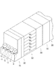
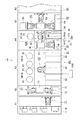
本発明の第1の実施形態に係る基板処理装置である塗布、現像装置1について図1〜図3を参照しながら説明する。図1、図2、図3は、夫々当該塗布、現像装置1の平面図、斜視図、概略縦断側面図である。塗布、現像装置1には、例えば液浸露光を行う露光装置A6が接続されている。塗布、現像装置1及び露光装置A6により、基板であるウエハWの表面におけるレジスト膜の形成、レジスト膜の露光、レジスト膜の現像を順次行い、レジスト膜にレジストパターンを形成するレジストパターン形成システムが構成されている。
(First embodiment)
A coating and developing
塗布、現像装置1は、キャリアブロックA1と、受け渡しブロックA2と、処理ブロックA3と、中間ブロックA4と、インターフェイスブロックA5とが、この順に水平方向に直線状に配置されて構成され、エンドブロックであるインターフェイスブロックA5には、中間ブロックA4とは反対側に露光装置A6が接続されている。ブロックA1〜A5について、隣り合うように配置されたブロックは、互いに接すると共に互いに区画されている。便宜上、以降の説明では、ブロックA1〜A5の配列方向を前後方向とし、キャリアブロックA1側を前方側、インターフェイスブロックA5側を後方側とする。
The coating / developing
図中11は、ウエハWを複数枚格納した状態で塗布、現像装置1の外部から搬送されるキャリアである。キャリアブロックA1は、キャリア11の載置台12と、キャリア11内とキャリアブロックA1内との間でウエハWを搬送するための搬送機構13と、を備えている。搬送機構13は、キャリア11と後述のタワーT1の受け渡しモジュールTRSとの間でウエハWの受け渡しを行うことができるように構成されている。なお、各実施形態の塗布、現像装置においてウエハWが載置される場所をモジュールと記載する。
In the figure,
続いて、受け渡しブロックA2について説明すると、当該受け渡しブロックA2の左右方向の中央部に、モジュールのタワーT1が設けられている。タワーT1は、当該受け渡しブロックA2と、キャリアブロックA1または処理ブロックA3との間でウエハWを受け渡すための多数の受け渡しモジュールTRSと、ウエハWの温度調整を行う多数の温度調整モジュールSCPLと、が積層されて構成されている。このタワーT1の受け渡しモジュールTRSのうち、搬送機構13によりウエハWの受け渡しが行われるモジュールについて、図3中、TRS0及びTRS7として示している。タワーT1におけるその他の受け渡しモジュールTRS及び温度調整モジュールSCPLの配置については後述する。
Next, the delivery block A2 will be described. A module tower T1 is provided at the center in the left-right direction of the delivery block A2. The tower T1 includes a number of delivery modules TRS for delivering the wafer W between the delivery block A2, the carrier block A1 or the processing block A3, a number of temperature adjustment modules SCPL for adjusting the temperature of the wafer W, Are laminated. Among the transfer modules TRS of the tower T1, the modules in which the wafer W is transferred by the
受け渡しブロックA2には、タワーT1を左右から挟むように搬送機構14、15が設けられている。前方から後方に向かって見て、タワーT1の右側の搬送機構を14、左側の搬送機構を15とする。これら搬送機構14、15は、タワーT1を構成する各モジュール間でウエハWを搬送することができるように、昇降自在に構成されている。前方から後方に向かって見て、搬送機構14の右側にはウエハWの表面にガスを供給して疎水化処理する疎水化処理モジュール16が設けられており、搬送機構14はタワーT1の各モジュールと疎水化処理モジュール16との間においても、ウエハWの受け渡しが行えるように構成されている。
In the delivery block A2,
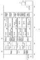
次に、処理ブロックA3について説明する。処理ブロックA3は、互いに区画された扁平な単位ブロックB1、B2、B3、B4、B5、B6が、下から上に向かってこの順で積層されて構成されている。単位ブロックB1〜B3は、露光装置A6による露光前のウエハWに反射防止膜及びレジスト膜を形成する単位ブロックである。単位ブロックB4〜B6は、露光装置A6による露光後のウエハWに現像処理を行う単位ブロックである。 Next, the processing block A3 will be described. The processing block A3 is configured by stacking flat unit blocks B1, B2, B3, B4, B5, and B6 that are partitioned from each other in this order from the bottom to the top. The unit blocks B1 to B3 are unit blocks for forming an antireflection film and a resist film on the wafer W before exposure by the exposure apparatus A6. The unit blocks B4 to B6 are unit blocks for performing development processing on the wafer W after exposure by the exposure apparatus A6.
単位ブロックB6について、図1を参照しながら説明する。図中21はウエハWの搬送領域であり、単位ブロックB6の左右の中央部において前後に伸びるように形成されている。前方から後方に向かって見て、搬送領域21の右側には多数の加熱モジュール22が設けられている。加熱モジュール22は複数上下に積層されて積層体を形成し、この積層体が前後方向に6つ配列されている。加熱モジュール22はウエハWが載置される熱板を備え、載置されたウエハWを所定の温度に加熱する。
The unit block B6 will be described with reference to FIG. In the figure,
また、前方から後方に向かって見て、搬送領域21の左側には、2つの現像モジュールDEV6が2つ前後に配置されている。現像モジュールDEV6は、前後に配列された2つのカップ23を備えており、各カップ23にウエハWが収納された状態で当該ウエハWに現像液が供給されて、現像処理が行われる。搬送領域21にはウエハWの搬送機構C6が設けられており、現像モジュールDEV6の各カップ23と、加熱モジュール22と、タワーT1及び後述のタワーT2に設けられるモジュールのうち単位ブロックB6に対応する高さに位置するモジュールと、に夫々ウエハWの受け渡しを行う。
Further, when viewed from the front to the rear, two developing modules DEV6 are arranged on the left side of the
単位ブロックB4、B5は、単位ブロックB6と同様に構成されている。図3では、単位ブロックB4、B5に設けられる現像モジュールをDEV4、DEV5として夫々示しており、単位ブロックB4、B5に設けられる搬送機構をC4、C5として夫々示している。単位ブロックB1〜B3については、2つの現像モジュールDEVの代わりに1つのレジスト膜形成モジュールCOT及び1つの反射防止膜形成モジュールBCTが設けられている。レジスト膜形成モジュールCOT及び反射防止膜形成モジュールBCTは現像モジュールDEVと略同様に構成されているが、カップ23に収納されたウエハWに現像液の代わりに、レジスト、反射防止膜形成用の薬液を供給して塗布を行う。このように現像モジュールDEVの代わりにレジスト膜形成モジュールCOT及び反射防止膜形成モジュールBCTが設けられていることを除いて、単位ブロックB1〜B3は、単位ブロックB4〜B6と同様に構成されている。
The unit blocks B4 and B5 are configured similarly to the unit block B6. In FIG. 3, the developing modules provided in the unit blocks B4 and B5 are shown as DEV4 and DEV5, respectively, and the transport mechanisms provided in the unit blocks B4 and B5 are shown as C4 and C5, respectively. For the unit blocks B1 to B3, one resist film forming module COT and one antireflection film forming module BCT are provided instead of the two developing modules DEV. The resist film forming module COT and the antireflection film forming module BCT are configured in substantially the same manner as the developing module DEV. However, instead of the developer on the wafer W accommodated in the
図3においては単位ブロックB1〜B3に設けられるレジスト膜形成モジュールをCOT1〜COT3として示しており、単位ブロックB1〜B3に設けられる反射防止膜形成モジュールをBCT1〜BCT3として示している。また、単位ブロックB1〜B3に設けられる搬送機構についてはC1〜C3として示している。搬送機構C1〜C6は、第3の基板搬送機構を構成する。この第1の実施形態では、現像モジュールDEV4〜DEV6において、レジスト膜における露光された領域を除去する現像(以下、ポジ型現像と記載する)を行うための現像液がウエハWに供給される。 In FIG. 3, the resist film forming modules provided in the unit blocks B1 to B3 are indicated as COT1 to COT3, and the antireflection film forming modules provided in the unit blocks B1 to B3 are indicated as BCT1 to BCT3. Further, the transport mechanisms provided in the unit blocks B1 to B3 are indicated as C1 to C3. The transport mechanisms C1 to C6 constitute a third substrate transport mechanism. In the first embodiment, in the development modules DEV4 to DEV6, a developing solution for performing development (hereinafter referred to as positive development) for removing an exposed area in the resist film is supplied to the wafer W.
ここで、上記の受け渡しブロックA2のタワーT1におけるモジュールの配置について補足して説明しておくと、搬送機構C1〜C6によりウエハWの受け渡しが行える各高さに、受け渡しモジュールTRS及び温度調整モジュールSCPLが設けられている。図3中、搬送機構C1〜C6によりウエハWを受け渡し可能な受け渡しモジュールTRSをTRS1〜TRS6、搬送機構C1〜C6によりウエハWを受け渡し可能な温度調整モジュールSCPLをSCPL1〜SCPL6として示している。 Here, the module arrangement in the tower T1 of the transfer block A2 will be described supplementarily. The transfer module TRS and the temperature adjustment module SCPL are set to heights at which the wafer W can be transferred by the transfer mechanisms C1 to C6. Is provided. In FIG. 3, the transfer modules TRS that can transfer the wafer W by the transfer mechanisms C1 to C6 are shown as TRS1 to TRS6, and the temperature adjustment modules SCPL that can transfer the wafer W by the transfer mechanisms C1 to C6 are shown as SCPL1 to SCPL6.
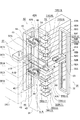
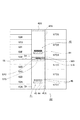
次に中間ブロックA4について、斜視図である図4及び後方から前方に向かって見た概略縦断背面図である図5も参照しながら説明する。中間ブロックA4の左右の中央部の前方側には、受け渡し部を構成するモジュールのタワーT2が設けられており、当該タワーT2は、多数の受け渡しモジュールTRS及び温度調整モジュールSCPLが上下に積層されることにより構成されている。
Next, the intermediate block A4 will be described with reference to FIG. 4 which is a perspective view and FIG. 5 which is a schematic longitudinal rear view seen from the rear to the front. A tower T2 of modules constituting a delivery unit is provided in front of the left and right central parts of the intermediate block A4. The tower T2 includes a number of delivery modules TRS and temperature adjustment modules SCPL stacked vertically. It is constituted by.
このタワーT2の受け渡しモジュールTRSについて、上記の単位ブロックB1〜B6に対応する各高さに設けられ、上記の搬送機構C1〜C6によってウエハWの受け渡しが夫々行われるモジュール(第1の載置モジュール)をTRS11〜TRS16として示している。また、タワーT2の下部側、上部側には、後述の下側搬送機構41、上側搬送機構42によりウエハWの受け渡しが行えるように受け渡しモジュールTRS17、TRS18が夫々設けられている。さらに、タワーT2の高さ中央部には、後述のシャトル57に対してウエハWの受け渡しを行う第2の載置モジュールである受け渡しモジュールTRS10が設けられている。また、温度調整モジュールSCPLについては、タワーT2の下部側、上部側に、下側搬送機構41、上側搬送機構42によって夫々ウエハWの受け渡しが行えるSCPL11、SCPL12が設けられている。
The transfer module TRS of the tower T2 is provided at each height corresponding to the unit blocks B1 to B6, and the module (first mounting module) in which the wafer W is transferred by the transfer mechanisms C1 to C6. ) Are shown as TRS11 to TRS16. Further, on the lower side and the upper side of the tower T2, transfer modules TRS17 and TRS18 are respectively provided so that the wafer W can be transferred by a
上記の受け渡しモジュールTRS11〜TRS18の構成について説明しておく。これら受け渡しモジュールTRS11〜TRS18は、夫々水平板と、当該水平板から上方へ突出したウエハWの裏面中心部を支持するための3本のピンと、を備え、処理ブロックA3の搬送機構C1〜C6、後述の下側搬送機構41、上側搬送機構42、上下間搬送機構31の昇降動作によって、このピンの先端にウエハWを受け渡すことができる。なお、上記のタワーT1における各受け渡しモジュールTRS及び後述のタワーT3におけるTRS20を除く各受け渡しモジュールTRSも、各搬送機構との間でウエハWを受け渡せるように、例えば受け渡しモジュールTRS11〜TRS18と同様に構成される。受け渡しモジュールTRS10については、昇降機構により昇降自在なウエハWの裏面中心部を支持するための3本の昇降ピンを備えており、後述のシャトル57と当該昇降ピンとの間でウエハWの受け渡しが行えるように構成されている。
The configuration of the delivery modules TRS11 to TRS18 will be described. Each of the delivery modules TRS11 to TRS18 includes a horizontal plate and three pins for supporting the center of the back surface of the wafer W protruding upward from the horizontal plate, and the transfer mechanisms C1 to C6 of the processing block A3. The wafer W can be transferred to the tip of this pin by the raising and lowering operations of the
温度調整モジュールSCPL11、SCPL12は、概ね円形のプレートを備えており、当該プレート上にウエハWが載置される。プレートの周縁部には切り欠きが形成され、当該切り欠きを後述の下側搬送機構41、上側搬送機構42の支持体46の爪部が通過することで、支持体46とプレートの間でウエハWの受け渡しが行われる。当該プレートの裏面には冷却水の流路が設けられており、プレートに載置されたウエハWの温度が調整される。なお、上記のタワーT1の温度調整モジュールSCPLも、この温度調整モジュールSCPL11、SCPL12と同様に構成されている。
The temperature adjustment modules SCPL11 and SCPL12 include a generally circular plate, and the wafer W is placed on the plate. A notch is formed in the peripheral portion of the plate, and a claw portion of the
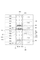
タワーT2を左右から挟むように、上下間搬送機構31と清浄気体供給部36とが設けられている。載置モジュール間搬送機構である上下間搬送機構31は、下側搬送機構41、上側搬送機構42と共に第1の基板搬送機構を構成する。図6も参照しながら、上下間搬送機構31について説明する。図6の上段、下段は夫々上下間搬送機構31の側面、上面を示している。上下間搬送機構31は、起立した縦長のフレーム状のガイド32と、ガイド32の長さ方向に沿って垂直に昇降する昇降台33と、昇降台33上にて進退自在に構成され、ウエハWの裏面を支持する支持体34と、を備えている。支持体34は、タワーT2の各受け渡しモジュールTRSに対してウエハWの受け渡しができるように、平面視概ねU字状に形成され、ウエハWの裏面中心部に重ならずにウエハWを支持する。上記のガイド32には、その長さ方向に沿ってスリット状の排気口35が、当該ガイド32の内側に向かって開口している。
A
清浄気体供給部36はフィルタを備えており、当該フィルタにより清浄化された気体をタワーT2に向けて、当該タワーT2の上端部から下端部に亘って供給できるように縦長に構成されている。塗布、現像装置1によるウエハWの搬送中に、清浄気体供給部36の清浄気体の供給と排気口35からの排気とが、互いに並行して行われる。それによってタワーT2の各モジュール間を通過し、さらに図6の上段に点線の矢印で示す上下間搬送機構31の昇降台33の昇降領域を通過するように、横方向に流れる気流が形成される。図6の上段及び下段で、当該気流を実線の矢印で示している。上下間搬送機構31からパーティクルが発生したり、タワーT2の周囲からパーティクルが発生しても、これらのパーティクルは上記の気流に乗って除去され、ウエハWに付着することが抑えられる。
The clean
図4、図5に戻って、中間ブロックA4の左右の中央部の後方側には、下側搬送機構41及び上側搬送機構42が、互いに上下に重なるように設けられている。下側搬送機構41及び上側搬送機構42は互いに同様に構成されており、代表して下側搬送機構41について説明すると、下側搬送機構41は起立した縦長のフレーム状のガイド43と、ガイド43の長さ方向に沿って垂直に昇降する昇降台44と、昇降台44上にて鉛直軸周りに回転自在な回転台45と、回転台45上に設けられるウエハWの支持体46、46と、を備えている。
Referring back to FIGS. 4 and 5, a
2つの支持体46、46は、そのうちの一方がモジュールからウエハWを受け取り、他方が当該モジュールにウエハWを搬送できるように、互いに独立して進退自在に構成されている。また、支持体46は、タワーT2の各温度調整モジュールSCPLに対してウエハWの受け渡しを行えるように、当該温度調整モジュールSCPLのプレートの形状に対応した構成とされている。具体的には、基端部から先端部が2又に分かれて水平に伸びると共にウエハWの側周を囲むように形成されたフレームと、温度調整モジュールSCPLのプレートの切り欠きに対応するようにフレームの内側に向けて突出してウエハWの裏面周縁部を支持する爪部と、により構成されている。
The two
前方から後方に向かって見て、下側搬送機構41、上側搬送機構42の右側には、周縁露光モジュール51A、51Bと加熱モジュール52A〜52Hと排気ユニット53A、53Bとが互いに積層されて設けられており、下方から上方に向けて、53A、52A、52B、52C、52D、51A、53B、52E、52F、52G、52H、51Bの順で設けられている。周縁露光モジュール51A、51Bは、夫々ウエハWの周縁部の不要なレジスト膜を除去するために、当該周縁部を露光する。この周縁露光モジュール51A、51Bは、露光前のウエハWの表面状態を検査するために、カメラによる撮像についても行えるように構成してもよい。加熱モジュール52A〜52Hは、処理ブロックA3の加熱モジュール22と同様に、載置されたウエハWを加熱する熱板を備えている。
When viewed from the front to the rear, the
前方から後方に向かって見て、下側搬送機構41及び上側搬送機構42の左側には、保護膜形成モジュールITC1〜ITC6が積層されて設けられている。この保護膜形成モジュールITC1〜ITC6による積層体は、周縁露光モジュール51A、51B、加熱モジュール52A〜52H及び排気ユニット53A、53Bからなる積層体と共に、下側搬送機構41及び上側搬送機構42を左右から挟むように設けられている。保護膜形成モジュールITC1〜ITC6は、夫々1つのカップ23を備えている。そして、当該カップ23に収納されたウエハWに保護膜形成用の薬液が供給され、露光装置A6による液浸露光時にレジスト膜を保護するための保護膜が形成される。6つの保護膜形成モジュールのうち、下側に設けられる3つをITC1〜ITC3、上側に設けられる3つをITC4〜ITC6として示している。
The protective film forming modules ITC1 to ITC6 are stacked and provided on the left side of the
上記の保護膜形成モジュールITC1〜ITC3、周縁露光モジュール51A、加熱モジュール52A〜52D及び温度調整モジュールSCPL11は、下側搬送機構41によってウエハWの受け渡しが行える高さに設けられている。そして、保護膜形成モジュールITC4〜ITC6、周縁露光モジュール51B、加熱モジュール52E〜52H及び温度調整モジュールSCPL12は、上側搬送機構42によってウエハWの受け渡しが行える高さに設けられている。また、下側搬送機構41、上側搬送機構42は、インターフェイスブロックA5に設けられる後述のタワーT3に設けられる受け渡しモジュールTRSにもウエハWの受け渡しを行う。
The protective film forming modules ITC <b> 1 to ITC <b> 3, the edge exposure module 51 </ b> A, the heating modules 52 </ b> A to 52 </ b> D, and the temperature adjustment module SCPL <b> 11 are provided at a height at which the
下側搬送機構41及び上側搬送機構42と各モジュールとのウエハWの受け渡しについて補足して説明しておくと、保護膜形成モジュールITC1〜ITC6のカップ23及び周縁露光モジュール51A、51Bには、図示しない昇降ピンが設けられており、当該昇降ピンを介してこれらのモジュールと下側搬送機構41または上側搬送機構42との間でウエハWの受け渡しが行われる。また、加熱モジュール52A〜52Hには、上記の温度調整モジュールSCPLのプレートと同様に形成されたウエハWの温度調整用のプレートと、当該プレートを熱板の外側と熱板の上方との間で移動させる移動機構と、熱板と当該熱板上に移動したプレートとの間でウエハWを受け渡すための昇降ピンと、が設けられている。この加熱モジュール52A〜52Hのプレートに対しては、当該プレートが熱板の外側に位置する状態で下側搬送機構41または上側搬送機構42の支持体46が昇降することでウエハWの受け渡しが行われる。
A supplemental description of the transfer of the wafer W between the
ところで各図中、保護膜形成モジュールITC1〜ITC3と、周縁露光モジュール51A及び加熱モジュール52A〜52Dとの間における下側搬送機構41によるウエハWの搬送領域を41Aとして示しており、保護膜形成モジュールITC4〜ITC6と、周縁露光モジュール51B及び加熱モジュール52E〜52Hとの間における上側搬送機構42によるウエハWの搬送領域を42Aとして示している。上記の排気ユニット53A、53Bは、各々排気口54を備えており、排気ユニット53Aの排気口54、排気ユニット53Bの排気口54は、夫々搬送領域41A、42Aに開口している。
By the way, in each figure, the transfer area of the wafer W by the
上記の搬送領域41A、42Aの間には、これら搬送領域41A、42Aを互いに区画するように清浄気体供給部41Bが設けられており、搬送領域42Aの上方には清浄気体供給部42Bが設けられている。清浄気体供給部41B、42Bは、内部に清浄気体の流路を備えた水平な厚板状に構成され、当該流路に供給される清浄気体が、清浄気体供給部41B、42Bの下面に分散して設けられる多数の孔から下方に向けて供給される。塗布、現像装置1によるウエハWの搬送中に、この清浄気体供給部41B、42Bからの清浄気体の供給と、上記の排気ユニット53A、53Bの排気口54からの排気とが行われる。それによって図5に矢印で示すように、搬送領域41A、42Aには、夫々上方から下方に向かい、当該搬送領域41A、42Aの下端部から横方向に流れて排気されるように下降気流が形成される。この下降気流によって、保護膜形成モジュールITC1〜ITC6にて発生した薬液のミストがパーティクルとなって搬送領域41A、42Aに流れたり、下側搬送機構41、上側搬送機構42からパーティクルが搬送領域41A、42Aに飛散しても、搬送領域41A、42Aから排除され、ウエハWに付着することが抑えられる。
A clean
清浄気体供給部41Bの上方且つ搬送領域42Aの下方には、第2の基板搬送機構であるシャトル57が設けられている。シャトル57は、前後方向に伸びるガイド57Aと、ガイド57Aに沿って前後に水平移動自在且つ前後に長尺に形成されたスライダー57Bと、ウエハWが載置されると共に、スライダー57Bの長さ方向に沿って当該スライダー57Bの一端上と他端上との間を移動自在に構成されたシャトル本体57Cと、を備えている。シャトル本体57Cは、上記のタワーT2の受け渡しモジュールTRS10上と、インターフェイスブロックA5に設けられるタワーT3の受け渡しモジュールTRS20上との間で搬送される。受け渡しモジュールTRS20は、上記の受け渡しモジュールTRS10と同様に構成されており、昇降ピンを備えている。受け渡しモジュールTRS10、TRS20の各昇降ピンは、当該受け渡しモジュールTRS10、TRS20上に移動するシャトル本体57Cに干渉せずに昇降し、当該シャトル本体57Cとの間でウエハWの受け渡しを行えるように配置されている。
A
シャトル57によるウエハWの搬送領域58は、下側搬送機構41によるウエハWの搬送領域41Aと、上側搬送機構42によるウエハWの搬送領域42Aとに重なると共に、これら搬送領域41A、42Aに上下から挟まれるように形成されている。図5に示すように、清浄気体供給部41Bの上方には仕切り板58Aが設けられており、この仕切り板58Aと清浄気体供給部41Bとにより、搬送領域58は、搬送領域41A及び搬送領域42Aから区画されている。なお、図5以外の図では仕切り板58Aの図示は省略している。
The wafer
続いて、図1、図3を参照しながらインターフェイスブロックA5について説明する。インターフェイスブロックA5は、左右の中央部にタワーT3を備えている。このタワーT3は、多数の積層された受け渡しモジュールTRSを含んでおり、このTRSとしては、上記のシャトル57によりウエハWの受け渡しが行われるTRS20と、下側搬送機構41、上側搬送機構42により夫々ウエハWの受け渡しが行われるTRS21、TRS22と、TRS23、TRS24とが含まれている。
Next, the interface block A5 will be described with reference to FIGS. The interface block A5 includes a tower T3 at the left and right central portions. The tower T3 includes a large number of stacked transfer modules TRS. The TRS includes a TRS 20 that transfers the wafer W by the
インターフェイスブロックA5には、搬送機構61〜63と、露光前にウエハの裏面を洗浄する裏面洗浄モジュール64、露光後にウエハWの表面を洗浄する表面洗浄モジュール65と、が設けられている。裏面洗浄モジュール64は、ウエハWの裏面に洗浄液を供給すると共に、ブラシによりウエハWを擦って洗浄する。表面洗浄モジュール65は、ウエハWの表面に洗浄液を供給して洗浄する。搬送機構61はタワーT3の受け渡しモジュールTRS21、TRS22と露光装置A6との間でウエハWを搬送できるように構成されている。搬送機構62、63は、タワーT3を構成する各受け渡しモジュールTRS間でウエハWを搬送できるように昇降自在に構成されており、搬送機構62は裏面洗浄モジュール64に、搬送機構63は表面洗浄モジュール65に、夫々ウエハWを受け渡すことができる。
The interface block A5 is provided with
図1に示すように塗布、現像装置1には制御部100が設けられている。制御部100は、例えばコンピュータからなり、不図示のプログラム格納部を有している。このプログラム格納部には、後述のウエハWの搬送及び各モジュールでのウエハWの処理が行われるように命令(ステップ群)が組まれたプログラムが格納されている。そのように格納された当該プログラムによって、各搬送機構によるウエハWの搬送、各処理モジュールにおけるウエハWの処理が行われるように制御部100から塗布、現像装置1の各部に制御信号が出力される。このプログラムは、例えばハードディスク、コンパクトディスク、マグネットオプティカルディスクまたはメモリーカードなどの記憶媒体に収納された状態でプログラム格納部に格納される。
As shown in FIG. 1, the coating and developing
上記の塗布、現像装置1における各搬送機構によるウエハWの搬送は互いに並行して行われ、各モジュールにおけるウエハWの処理についても互いに並行して行われる。続いて、上記の塗布、現像装置1におけるウエハWの搬送経路と処理工程とについて、図3及び図7を参照しながら説明する。図7は、ウエハWが搬送されるモジュールを順番に示すと共に、各モジュールにウエハWを受け渡す搬送機構を当該モジュールに対応付けて示している。図3では実線の矢印により、一部の受け渡しモジュールTRSに対するウエハWの搬送方向を示している。
The transfer of the wafer W by each transfer mechanism in the coating and developing
キャリア11からキャリアブロックA1の搬送機構13により搬出されたウエハWは、タワーT1の受け渡しモジュールTRS0に搬送され、受け渡しブロックA2の搬送機構14により疎水化処理モジュール16に搬送されて疎水化処理された後、搬送機構14により受け渡しモジュールTRS1、TRS2、TRS3のうちのいずれかに搬送される。つまり、ウエハWは、単位ブロックB1、B2、B3のうちのいずれかに搬入されるように振り分けられる。
The wafer W unloaded from the
受け渡しモジュールTRS1に搬送されたウエハWは、搬送機構C1により、タワーT1の温度調整モジュールSCPL1→反射防止膜形成モジュールBCT1→加熱モジュール22→温度調整モジュールSCPL1→レジスト膜形成モジュールCOT1→加熱モジュール22の順で搬送される。それによって、ウエハWの表面に反射防止膜が形成された後、反射防止膜を被覆するようにレジスト膜が形成される。然る後、搬送機構C1により中間ブロックA4におけるタワーT2の受け渡しモジュールTRS11に受け渡される。
The wafer W transferred to the delivery module TRS1 is transferred by the transfer mechanism C1 to the temperature adjustment module SCPL1 of the tower T1, the antireflection film formation module BCT1, the
受け渡しモジュールTRS2、TRS3に搬送されたウエハWは、搬送機構C2、C3により夫々搬送されること、及び単位ブロックB2、B3の高さに対応するモジュールに搬送されることを除いて、受け渡しモジュールTRS1に搬送されたウエハWと同様に搬送されて処理される。具体的に搬送経路を説明すると、受け渡しモジュールTRS2に搬送されたウエハWは、温度調整モジュールSCPL2→反射防止膜形成モジュールBCT2→加熱モジュール22→温度調整モジュールSCPL2→レジスト膜形成モジュールCOT2→加熱モジュール22→タワーT2の受け渡しモジュールTRS12の順で搬送されて、受け渡しモジュールTRS3に搬送されたウエハWは、温度調整モジュールSCPL3→反射防止膜形成モジュールBCT3→加熱モジュール22→温度調整モジュールSCPL3→レジスト膜形成モジュールCOT3→加熱モジュール22→受け渡しモジュールTRS13の順で搬送される。
The wafer W transferred to the transfer modules TRS2 and TRS3 is transferred by the transfer mechanisms C2 and C3, respectively, and transferred to the module corresponding to the height of the unit blocks B2 and B3. Are transferred and processed in the same manner as the wafer W transferred to the wafer. Specifically, the transfer path is as follows. The wafer W transferred to the delivery module TRS2 is the temperature adjustment module SCPL2 → the antireflection film formation module BCT2 → the
タワーT2の受け渡しモジュールTRS11〜TRS13に搬送されたウエハWは、中間ブロックA4の上下間搬送機構31により、受け渡しモジュールTRS17またはTRS18に振り分けられるように搬送される。そして、受け渡しモジュールTRS17に搬送されたウエハWは、下側搬送機構41により、温度調整モジュールSCPL11→保護膜形成モジュールITC1〜ITC3のうちのいずれか→加熱モジュール52A〜52Dのうちのいずれか→周縁露光モジュール51Aの順で搬送される。それによって、レジスト膜の上層に保護膜が形成され、さらに保護膜を介してレジスト膜の周縁部が露光される。然る後、ウエハWは下側搬送機構41により、インターフェイスブロックA5のタワーT3の受け渡しモジュールTRS21に搬送される。
The wafer W transferred to the transfer modules TRS11 to TRS13 of the tower T2 is transferred so as to be distributed to the transfer module TRS17 or TRS18 by the
受け渡しモジュールTRS18に搬送されたウエハWは、上側搬送機構42により搬送されること、及びこの上側搬送機構42の高さに対応するモジュールに搬送されることを除いて、受け渡しモジュールTRS17に搬送されたウエハWと同様に搬送されて処理される。具体的に搬送経路を説明すると、受け渡しモジュールTRS18→温度調整モジュールSCPL12→保護膜形成モジュールITC4〜ITC6のうちのいずれか→加熱モジュール52E〜52Hのうちのいずれか→周縁露光モジュール51B→タワーT3の受け渡しモジュールTRS22の順で搬送される。
The wafer W transferred to the transfer module TRS18 was transferred to the transfer module TRS17 except that the wafer W was transferred by the
受け渡しモジュールTRS21、TRS22に搬送されたウエハWは、搬送機構62により裏面洗浄モジュール64に搬送されて裏面洗浄された後、受け渡しモジュールTRS23に搬送され、搬送機構61により露光装置A6に搬送されて露光され、然る後、搬送機構61により受け渡しモジュールTRS24に搬送される。その後、搬送機構63により表面洗浄モジュール65に搬送されて、表面洗浄された後、タワーT3の受け渡しモジュールTRS20に搬送され、シャトル57によりタワーT2の受け渡しモジュールTRS10に直通で搬送される。つまり、中間ブロックA4の処理モジュールである保護膜形成モジュールITC1〜6、加熱モジュール52A〜H、周縁露光モジュール51A、51Bを素通りするように搬送される。
The wafer W transferred to the transfer modules TRS21 and TRS22 is transferred to the back
その後、上下間搬送機構31によりウエハWは、受け渡しモジュールTRS10から受け渡しモジュールTRS14、TRS15、TRS16のうちのいずれかに搬送される。つまり、ウエハWは、単位ブロックB4、B5、B6のうちのいずれかに搬入されるように振り分けられる。受け渡しモジュールTRS14に搬送されたウエハWは、搬送機構C4により、加熱モジュール22→タワーT1の温度調整モジュールSCPL4→現像モジュールDEV4の順で搬送される。それによって、ウエハWは、露光後加熱処理、現像処理を順に受けてレジスト膜にレジストパターンが形成される。然る後、搬送機構C4によりウエハWは加熱モジュール22に搬送されて現像後加熱処理を受けた後、受け渡しブロックA2におけるタワーT1の受け渡しモジュールTRS4に搬送される。
Thereafter, the wafer W is transferred from the transfer module TRS10 to any one of the transfer modules TRS14, TRS15, and TRS16 by the
受け渡しモジュールTRS15、TRS16に搬送されたウエハWは、搬送機構C5、C6により夫々搬送されること、及び単位ブロックB5、B6の高さに対応するモジュールに搬送されることを除いて、受け渡しモジュールTRS14に搬送されたウエハWと同様に搬送されて処理される。具体的に搬送経路を説明すると、受け渡しモジュールTRS15に搬送されたウエハWは、加熱モジュール22→温度調整モジュールSCPL5→現像モジュールDEV5→加熱モジュール22→タワーT1の受け渡しモジュールTRS5の順で搬送される。受け渡しモジュールTRS16に搬送されたウエハWは、加熱モジュール22→温度調整モジュールSCPL6→現像モジュールDEV6→加熱モジュール22→タワーT1の受け渡しモジュールTRS6の順で搬送される。受け渡しモジュールTRS4〜TRS6に搬送されたウエハWは、受け渡しブロックA2の搬送機構15によりタワーT1の受け渡しモジュールTRS7に搬送され、キャリアブロックA1の搬送機構13によりキャリア11に戻される。
The wafer W transferred to the transfer modules TRS15 and TRS16 is transferred by the transfer mechanisms C5 and C6, and transferred to the module corresponding to the height of the unit blocks B5 and B6. Are transferred and processed in the same manner as the wafer W transferred to the wafer. Specifically, the transfer path will be described. The wafer W transferred to the transfer module TRS15 is transferred in the order of the
この塗布、現像装置1によれば、処理ブロックA3においてレジスト膜が形成された露光前のウエハWに対して各種の処理を行う中間ブロックA4が設けられ、この中間ブロックA4には、多数の保護膜形成モジュールITC1〜6からなる処理モジュールの積層体と、多数の加熱モジュール52A〜H及び複数の周縁露光モジュール51A、51Bからなる処理モジュールの積層体と、処理ブロックA3から中間ブロックA4にウエハWを受け渡すため受け渡しモジュールTRSが積層されるタワーT2と、タワーT2の受け渡しモジュールTRSから上記の各積層体をなすモジュールにウエハWを搬送し、当該モジュールにて処理済みのウエハWをインターフェイスブロックA5に搬送する上下間搬送機構31、下側搬送機構41及び上側搬送機構42と、露光済みのウエハWを現像するためにインターフェイスブロックA5の受け渡しモジュールTRS20からタワーT2の受け渡しモジュールTRS10へ直通でウエハWを搬送するシャトル57と、が設けられている。上記のように処理モジュールの積層体を形成することで、中間ブロックA4に設けられる保護膜形成モジュールITC1〜6、加熱モジュール52A〜H、周縁露光モジュール51A、51B夫々の個数の増加を図りつつ、中間ブロックA4ひいては塗布、現像装置1のフットプリントの上昇を抑えることができる。そして、シャトル57が設けられていることで、速やかに露光済みのウエハWを処理ブロックA3に戻すことができ、上記の各処理モジュールの積層体に対してウエハWを受け渡す下側搬送機構41及び上側搬送機構42が露光済みのウエハWを処理ブロックA3に戻すために動作する必要が無く、これら下側搬送機構41及び上側搬送機構42の負担が抑えられる。結果として、装置のスループットの向上を図ることができる。
According to the coating / developing
また、保護膜形成モジュールITC1〜ITC6の積層体、加熱モジュール52A〜52H、周縁露光モジュール51A、51Bの積層体、及びタワーT2の温度調整モジュールSCPL11、12について、下側に配置されたモジュールについては下側搬送機構41がウエハWを受け渡し、上側に配置されたモジュールについては上側搬送機構42がウエハWを受け渡す。このように互いに積層された同種の複数のモジュールについて、互いに異なる搬送機構41、42がウエハWの受け渡しを行うように割り当てられていることで、各搬送機構41、42の負担が確実に抑えられ、より確実にスループットの向上を図ることができる。上記の同種のモジュールとは、キャリア11からのウエハWが搬送される順番が同じであり、互いにウエハWに同じ処理を行うモジュールである。
In addition, regarding the laminated body of the protective film forming modules ITC1 to ITC6, the
さらに、下側搬送機構41及び上側搬送機構42は上下に重なるように配置されているため、これら下側搬送機構41及び上側搬送機構42を設けることによる中間ブロックA4のフットプリントの上昇が抑えられる。さらに上記のシャトル57によるウエハWの搬送領域58は、下側搬送機構41によるウエハWの搬送領域41A及び上側搬送機構42によるウエハWの搬送領域42Aに重なるように設けられている。従って、より確実に中間ブロックA4のフットプリントを抑えることができる。
Furthermore, since the
(第2の実施形態)
続いて、第2の実施形態に係る塗布、現像装置7について、塗布、現像装置1との差異点を中心に説明する。図8、図9は夫々塗布、現像装置7の平面図、概略縦断側面図である。また、図10は、塗布、現像装置7の中間ブロックA4における概略縦断背面図である。この塗布、現像装置7の中間ブロックA4には、保護膜形成モジュールITC1〜ITC6の代わりに現像モジュールNTD1〜NTD6が設けられている。
(Second Embodiment)
Next, the coating and developing
保護膜形成モジュールITC1〜6との差異点として、現像モジュールNTD1〜NTD6は、保護膜形成用の薬液の代わりにレジスト膜における露光されていない領域を除去する現像(以下、ネガ型現像と記載する)を行うための現像液をウエハWに供給する。塗布、現像装置7では、レジスト膜が形成された後、ポジ型現像を行う場合、当該ウエハWは現像モジュールDEV4〜DEV6に搬送されて現像処理され、ネガ型現像を行う場合、当該ウエハWは現像モジュールNTD1〜NTD6に搬送されて現像処理される。
As a difference from the protective film forming modules ITC1 to ITC6 , the developing modules NTD1 to NTD6 are developed to remove an unexposed region in the resist film instead of the chemical solution for forming the protective film (hereinafter referred to as negative development). ) Is supplied to the wafer W. In the coating and developing
塗布、現像装置1と同様に塗布、現像装置7では、中間ブロックA4において、加熱モジュール52A〜52Hが積層されて設けられている。ただし、塗布、現像装置7における加熱モジュール52A〜52Hは、その役割について塗布、現像装置1の加熱モジュール52A〜52Hと異なり、露光後のウエハWの加熱を行う。また、この第2の実施形態における中間ブロックA4には、周縁露光モジュール51A、51Bが設けられていない。例えば周縁露光モジュールは、単位ブロックB1〜B3の加熱モジュール22に積層して設けておき、ウエハWはレジスト塗布後に各単位ブロックB1〜B3にて周縁露光処理されるようにしてもよい。
In the coating / developing
塗布、現像装置7において、ウエハWにレジストを供給してネガ型現像する場合のウエハWの搬送経路を、図11を参照しながら、第1の実施形態の塗布、現像装置1におけるウエハWの搬送経路との差異点を中心に説明する。キャリア11から搬送されたウエハWは、第1の実施形態と同様に単位ブロックB1〜B3に振り分けられて、反射防止膜の形成及びレジスト膜が形成された後、中間ブロックA4におけるタワーT2の受け渡しモジュールTRS11〜TRS13に搬送される。その後、ウエハWは、上下間搬送機構31→受け渡しモジュールTRS10→シャトル57→インターフェイスブロックA5の受け渡しモジュールTRS20の順で搬送され、受け渡しモジュールTRS20から搬送機構62に受け渡される。その後、ウエハWは第1の実施形態と同様にインターフェイスブロックA5内及びインターフェイスブロックA5と露光装置A6との間を受け渡され、裏面洗浄処理、露光処理、表面洗浄処理を順に受ける。
In the coating / developing
表面洗浄モジュール65から搬出されたウエハWは、搬送機構63により受け渡しモジュールTRS21、TRS22に振り分けられて搬送される。受け渡しモジュールTRS21に搬送されたウエハWは、下側搬送機構41により、加熱モジュール52A〜52Dのうちのいずれか→タワーT2の温度調整モジュールSCPL11→現像モジュールNTD1〜NTD3のうちのいずれかの順で受け渡され、露光後加熱処理、現像処理を順に受けた後、受け渡しモジュールTRS17に受け渡される。
The wafer W unloaded from the
受け渡しモジュールTRS22に搬送されたウエハWは、上側搬送機構42により搬送されること、及び上側搬送機構42の高さに対応するモジュールに搬送されることを除いて、受け渡しモジュールTRS21に搬送されたウエハWと同様に搬送されて処理される。具体的に搬送経路を説明すると、当該ウエハWは、加熱モジュール52E〜52Hのうちのいずれか→温度調整モジュールSCPL12→現像モジュールNTD4〜NTD6のうちのいずれか→受け渡しモジュールTRS18の順で搬送される。
The wafer W transferred to the transfer module TRS22 is transferred to the module corresponding to the height of the
受け渡しモジュールTRS17、TRS18に搬送されたウエハWは、上下間搬送機構31により、受け渡しモジュールTRS14、TRS15、TRS16のうちのいずれかに受け渡されるように搬送される。つまりウエハWは、単位ブロックB4、B5、B6のうちのいずれかに振り分けられるように搬送される。
受け渡しモジュールTRS14に搬送されたウエハWは、搬送機構C4により、加熱モジュール22に搬送されて現像後加熱処理を受けた後、温度調整モジュールSCPL4→受け渡しモジュールTRS4の順で搬送される。
The wafer W transferred to the transfer modules TRS17 and TRS18 is transferred by the
The wafer W transferred to the transfer module TRS14 is transferred to the
受け渡しモジュールTRS15、TRS16に搬送されたウエハWは、搬送機構C5、C6により夫々搬送されること、及び単位ブロックB5、B6の高さに対応するモジュールに搬送されることを除いて、受け渡しモジュールTRS14に搬送されたウエハWと同様に搬送されて加熱処理、温度調整処理を順に受け、受け渡しモジュールTRS5、TRS6に夫々受け渡される。然る後、受け渡しモジュールTRS4〜TRS6に搬送されたウエハWは、搬送機構15により受け渡しモジュールTRS7に搬送され、搬送機構13によりキャリア11に戻される。
The wafer W transferred to the transfer modules TRS15 and TRS16 is transferred by the transfer mechanisms C5 and C6, and transferred to the module corresponding to the height of the unit blocks B5 and B6. Are transferred in the same manner as the wafer W transferred, and are subjected to heating processing and temperature adjustment processing in order, and are transferred to the transfer modules TRS5 and TRS6, respectively. Thereafter, the wafer W transferred to the transfer modules TRS4 to TRS6 is transferred to the transfer module TRS7 by the
この塗布、現像装置7において、ウエハWにレジストを供給してポジ型現像する場合のウエハWの搬送経路と処理工程とを説明する。ネガ型現像をする場合と同様に、ウエハWは、キャリアブロックA1→受け渡しブロックA2→処理ブロックA3の単位ブロックB1〜B3→中間ブロックA4のシャトル57→インターフェイスブロックA5→露光装置A6→インターフェイスブロックA5の順で搬送されて順次処理を受ける。
In the coating / developing
その後、ウエハWは中間ブロックA4に搬送されて、加熱モジュール52A〜52Hで露光後の加熱処理を受けた後、下側搬送機構41、上側搬送機構42及び上下間搬送機構31により受け渡しモジュールTRS14〜TRS16のうちのいずれかに搬送されて、単位ブロックB4〜B6に振り分けられる。その後、ウエハWは第1の実施形態と同様に各単位ブロックB4〜B6内を搬送され、現像モジュールDEV4〜DEV6にて現像処理を受けた後に、キャリア11に戻される。この塗布、現像装置7についても、塗布、現像装置1と同様の効果が得られる。
After that, the wafer W is transferred to the intermediate block A4 and subjected to the heat treatment after exposure by the
(第3の実施形態)
第3の実施形態の塗布、現像装置71について、第1の実施形態の塗布、現像装置1との差異点を中心に、図12の平面図を参照しながら説明する。この塗布、現像装置71においては、処理ブロックA3とインターフェイスブロックA5との間に、前方から後方に向かって中間ブロックA41、A42、A43が設けられている。中間ブロックA41、A42、A43、インターフェイスブロックA5は、互いに隣接して設けられると共に、互いに区画されている。中間ブロックA41、A42、A43は、塗布、現像装置1における中間ブロックA4と同様に形成されている。
(Third embodiment)
The coating and developing
図13は、中間ブロックA41、A42、A43の概略縦断側面図である。中間ブロックA41、A42、A43において、タワーT2に相当する各タワーはT21、T22、T23として示している。また、タワーT22、T23の下部側に設けられ、後述するように前方側のブロックからウエハWを搬入するための受け渡しモジュールをTRS19として示している。この塗布、現像装置71において、ウエハWは中間ブロックA41、A42、A43のうちのいずれかにて、温度調整モジュールSCPL、保護膜形成モジュールITC1〜ITC6、加熱モジュール52A〜52H及び周縁露光モジュール51A、51Bによる処理を順に受ける。
FIG. 13 is a schematic longitudinal side view of the intermediate blocks A41, A42, A43. In the intermediate blocks A41, A42, and A43, each tower corresponding to the tower T2 is indicated as T21, T22, and T23. In addition, a delivery module that is provided on the lower side of the towers T22 and T23 and carries the wafer W from the front block as shown below is indicated as TRS19. In the coating and developing
塗布、現像装置71における具体的な搬送の一例を示すと、単位ブロックB1〜B3を搬送されてレジスト膜が形成されたウエハWは、中間ブロックA41のタワーT21の受け渡しモジュールTRS11〜TRS13に受け渡される。中間ブロックA41で上記の各処理を受ける場合、当該ウエハWは、受け渡しモジュールTRS11〜TRS13→中間ブロックA41の上下間搬送機構31→タワーT21の受け渡しモジュールTRS17、TRS18の順で搬送されて中間ブロックA41の下側搬送機構41または上側搬送機構42に受け渡され、当該中間ブロックA41において第1の実施形態と同様に各モジュール間を搬送されて処理される。その後、中間ブロックA41を下側搬送機構41により搬送されたウエハWは、例えば中間ブロックA42、A43の下側搬送機構41及びタワーT22、T23の受け渡しモジュールTRS17を介してインターフェイスブロックA5のタワーT3の受け渡しモジュールTRS21へ搬送され、中間ブロックA41を上側搬送機構42により搬送されたウエハWは、中間ブロックA42、A43の上側搬送機構42及びタワーT22、T23の受け渡しモジュールTRS18を介してタワーT3の受け渡しモジュールTRS22へ搬送される。
An example of specific transport in the coating and developing
タワーT21の受け渡しモジュールTRS11〜TRS13に受け渡されたウエハWが、中間ブロックA42で処理を受ける場合、例えば当該ウエハWは、中間ブロックA41の下側搬送機構41→タワーT22の受け渡しモジュールTRS19→中間ブロックA42の上下間搬送機構31→タワーT22の受け渡しモジュールTRS17、TRS18に受け渡され、中間ブロックA42の下側搬送機構41及び上側搬送機構42により、当該中間ブロックA42内を搬送されて処理される。その後、中間ブロックA41で処理されたウエハWと同様に、タワーT23の各受け渡しモジュールTRS17、TRS18及び中間ブロックA43の下側搬送機構41、上側搬送機構42を介してタワーT3の受け渡しモジュールTRS21、TRS22へ搬送される。タワーT21の受け渡しモジュールTRS11〜TRS13に受け渡されたウエハWが、中間ブロックA43で処理を受ける場合、例えば当該ウエハWは、中間ブロックA41の下側搬送機構41→タワーT22の受け渡しモジュールTRS19→中間ブロックA42の下側搬送機構41→タワーT23の受け渡しモジュールTRS19→中間ブロックA43の上下間搬送機構31→タワーT23の受け渡しモジュールTRS17、TRS18に受け渡され、中間ブロックA43の下側搬送機構41及び上側搬送機構42により、当該中間ブロックA43にて搬送されて処理された後、タワーT3の受け渡しモジュールTRS21、TRS22へ受け渡される。
When the wafer W transferred to the transfer modules TRS11 to TRS13 of the tower T21 is processed in the intermediate block A42, for example, the wafer W is transferred to the
然る後、タワーT3の受け渡しモジュールTRS20に搬送された露光済みのウエハWは、中間ブロックA43のシャトル57→タワーT23の受け渡しモジュールTRS10→中間ブロックA42のシャトル57→タワーT22の受け渡しモジュールTRS10→中間ブロックA41のシャトル57→タワーT21の受け渡しモジュールTRS10の順で搬送され、以降、第1の実施形態と同様に単位ブロックB4〜B6に搬送されて現像処理される。
Thereafter, the exposed wafer W transferred to the transfer module TRS20 of the tower T3 is transferred from the
この塗布、現像装置71のように中間ブロックA4は複数設けることができ、それによって、装置のフットプリントの増大を抑えつつ、モジュール数のさらなる増加を図ることができる。第2の実施形態の塗布、現像装置7についても、この塗布、現像装置71のように中間ブロックを複数設けてもよい。
A plurality of intermediate blocks A4 can be provided like the coating / developing
(第4の実施形態)
第4の実施形態の塗布、現像装置72について、塗布、現像装置1との差異点を中心に、図14の平面図を参照しながら説明する。この塗布、現像装置72に関しては、中間ブロックA4の配置が塗布、現像装置1とは異なっており、受け渡しブロックA2と処理ブロックA3との間に中間ブロックA4が設けられている。また、中間ブロックA4において、保護膜形成モジュールITC1〜6の代わりに裏面洗浄モジュール64と同様に構成された裏面洗浄モジュール73が複数積層されて設けられ、現像処理が行われたウエハWはキャリア11に戻される前に、当該裏面洗浄モジュール73に搬送されて洗浄される。
(Fourth embodiment)
A coating / developing
塗布、現像装置72の中間ブロックA4には、加熱モジュール52A〜52H及び周縁露光モジュール51A、51Bが設けられていない。また、下側搬送機構41及び上側搬送機構42が、受け渡しブロックA2のタワーT1を構成するモジュールにウエハWを受け渡せるように、中間ブロックA4内の前方側に配置されている。そして、タワーT2及び上下間搬送機構31が中間ブロックA4内の後方側に配置されており、タワーT2を構成する各モジュールには、各単位ブロックB1〜B6の搬送機構C1〜C6によりウエハWが受け渡される。
In the intermediate block A4 of the coating and developing
図15には、タワーT1及びタワーT2におけるモジュールの配置の一例を示している。塗布、現像装置1のタワーT1において各単位ブロックB1〜B6に対応して設けられる受け渡しモジュールTRS1〜TRS6及び温度調整モジュールSCPL1〜SCPL6は、塗布、現像装置72ではタワーT2に設けられている。また、タワーT2には、下側搬送機構41、上側搬送機構42により夫々ウエハWの受け渡しが行われる受け渡しモジュールTRS31、TRS32が設けられている。
FIG. 15 shows an example of the arrangement of modules in the tower T1 and the tower T2. The transfer modules TRS1 to TRS6 and the temperature adjustment modules SCPL1 to SCPL6 provided corresponding to the unit blocks B1 to B6 in the tower T1 of the coating and developing
塗布、現像装置72のタワーT1には、塗布、現像装置1と同様にキャリアブロックA1の搬送機構13によりウエハWの受け渡しが行われる受け渡しモジュールTRS0、TRS7が設けられる他に、下側搬送機構41、上側搬送機構42により夫々ウエハWの受け渡しが行われる受け渡しモジュールTRS41、TRS42が夫々設けられている。インターフェイスブロックA5のタワーT3については図示を省略しているが、各単位ブロックB1〜B6に対応する高さに受け渡しモジュールTRSが設けられており、インターフェイスブロックA5の搬送機構62、63と、単位ブロックB1〜B6の各搬送機構C1〜C6との間でウエハWの受け渡しが行えるように構成されている。
The tower T1 of the coating / developing
塗布、現像装置72のウエハWの搬送経路について、塗布、現像装置1との差異点を中心に説明する。キャリア11のウエハWは、搬送機構13→受け渡しモジュールTRS0→受け渡しブロックA2の搬送機構14→疎水化処理モジュール16→搬送機構14→タワーT1の受け渡しモジュールTRS20→シャトル57→タワーT2の受け渡しモジュールTRS10→上下間搬送機構31→タワーT2の受け渡しモジュールTRS1〜TRS3のいずれかの順で搬送され、単位ブロックB1〜B3に搬入される。
The conveyance path of the wafer W of the coating / developing
露光処理を受け、インターフェイスブロックA5のタワーT3の受け渡しモジュールTRSを介して単位ブロックB4〜B6のいずれかに搬送されて現像処理されたウエハWは、タワーT2の受け渡しモジュールTRS4〜TRS6のいずれか→上下間搬送機構31→受け渡しモジュールTRS31またはTRS32→下側搬送機構41または上側搬送機構42→下側搬送機構41または上側搬送機構42が搬送可能な高さの裏面洗浄モジュール73→下側搬送機構41または上側搬送機構42→受け渡しモジュールTRS41またはTRS42→受け渡しブロックA2の搬送機構15→受け渡しモジュールTRS7→搬送機構13→キャリア11の順で搬送される。この塗布、現像装置72についても塗布、現像装置1と同様の効果が得られる。
The wafer W which has been subjected to the exposure process, transferred to any of the unit blocks B4 to B6 via the transfer module TRS of the tower T3 of the interface block A5 and developed, is one of the transfer modules TRS4 to TRS6 of the tower T2.
ところで、図5で説明した塗布、現像装置1の中間ブロックA4においては、同種のモジュールについて、下側搬送機構41によりウエハWが受け渡されるモジュールと、上側搬送機構42によりウエハWが受け渡されるモジュールとが同数となるように、下側搬送機構41、上側搬送機構42及びシャトル57による各搬送領域41A、42A、58が形成されているが、このように各搬送領域を形成することには限られない。図16に示す中間ブロックA4の例では、下側から上側に向けて排気ユニット53A、周縁露光モジュール51A、加熱モジュール52A〜52C、排気ユニット53B、周縁露光モジュール51B、51C、加熱モジュール52D〜52Iが積層されて設けられている。そして、下側搬送機構41が、保護膜形成モジュールITC1、ITC2、周縁露光モジュール51A及び加熱モジュール52A〜52CにウエハWを搬送し、上側搬送機構42が保護膜形成モジュールITC3〜ITC6、周縁露光モジュール51B、51C、加熱モジュール52D〜52IにウエハWを搬送するように、各搬送領域41A、42A、58が形成されている。
By the way, in the intermediate block A4 of the coating and developing
ただし、下側搬送機構41及び上側搬送機構42との間で搬送の負担が偏ることを抑えてスループットを向上させるためには、図5に示したように積層された同種のモジュールについて、下側搬送機構41によりウエハWが受け渡されるモジュールと、上側搬送機構42によりウエハWが受け渡されるモジュールとが同数となるように各搬送領域を形成することが有効である。
However, in order to suppress the burden of conveyance between the
また、図5に示した中間ブロックA4において、下側搬送機構41及び上側搬送機構42のうちのいずれか一方の搬送機構のみを設け、この一方の搬送機構が、積層された保護膜形成モジュールITC1〜ITC6、周縁露光モジュール51A、51B、加熱モジュール52A〜52HにウエハWを搬送するようにしてもよい。その場合、例えばシャトル57によるウエハWの搬送領域58は、一方の搬送機構によるウエハWの搬送領域の上側または下側に形成される。
Further, in the intermediate block A4 shown in FIG. 5, only one of the
また、シャトル57によるウエハWの搬送領域58は、下側搬送機構41の搬送領域41A及び上側搬送機構42の搬送領域42Aに対して上下に重なるように設けられることには限られない。図17は、図1で説明した中間ブロックA4の変形例であり、受け渡しモジュールTRS10、TRS20がタワーT2、タワーT3から左右方向にずれた位置に配置されている。そして、積層された加熱モジュール間がシャトル57の搬送領域58として構成され、当該シャトル57により、TRS10、TRS20間でウエハWが受け渡される。上下間搬送機構31の支持体34は鉛直軸周りに回転することで、受け渡しモジュールTRS10とタワーT2の各モジュールとの間でウエハWを受け渡すことができる。受け渡しモジュールTRS20は、搬送機構62によりウエハWの受け渡しが可能な位置に配置される。
Further, the
ところで、第4の実施形態の塗布、現像装置72において、キャリアブロックA1から搬出されたウエハWは、各ブロックA3〜A5及び露光装置A6で、レジスト塗布処理、現像処理などの各処理を受けずに中間ブロックA4に受け渡され、裏面洗浄モジュール73による処理を受けてキャリア11に戻されるようにしてもよい。つまり、本発明はウエハWの洗浄装置として構成することが可能である。同様に、第1の実施形態の塗布、現像装置1において、キャリア11から搬出されたウエハWについて、レジスト塗布処理及び現像処理を行わず、中間ブロックA4にて保護膜形成処理のみを行い、キャリア11に戻すようにしてもよい。つまり、本発明は保護膜形成装置として構成することが可能である。このように、本発明は、塗布、現像装置に適用されることには限られない。また、各実施形態で説明した例は互いに組み合わせることができる。例えば、第4の実施形態で説明した裏面洗浄モジュール73を備えた中間ブロックA4を第1及び第2の実施形態の各塗布、現像装置1、7における受け渡しブロックA2と処理ブロックA3との間に設けてもよい。
By the way, in the coating and developing
A1 キャリアブロック
A2 受け渡しブロック
A3 処理ブロック
A4 中間ブロック
B1〜B6 単位ブロック
ITC 保護膜形成モジュール
NTD 現像モジュール
SCPL 温度調整モジュール
TRS 受け渡しモジュール
W ウエハ
1、7、71、72 塗布、現像装置
31 上下共用搬送機構
51 下側搬送機構
52 上側搬送機構
57 シャトル
73 裏面洗浄モジュール
A1 Carrier block A2 Delivery block A3 Processing block A4 Intermediate block B1 to B6 Unit block ITC Protective film forming module NTD Development module SCPL Temperature adjustment module TRS Delivery
Claims (11)
前記中間ブロックは、
前記キャリアブロックから払い出されて前記エンドブロックに向かう前記基板、及び前記エンドブロックから前記キャリアブロックに戻される前記基板のうちの一方のみを各々処理するために、互いに積層されて設けられた複数の第1の処理モジュールと、
前記キャリアブロック及び前記エンドブロックのうちの一方から当該中間ブロックに搬送された前記基板を前記各第1の処理モジュールに搬送し、前記キャリアブロック及びエンドブロックのうちの他方に受け渡すために昇降する第1の基板搬送機構と、
前記キャリアブロック及び前記エンドブロックのうち他方から一方に前記第1の処理モジュールを素通りするように基板を搬送する、前記第1の基板搬送機構とは別体の第2の基板搬送機構と、
を備え、
前記キャリアブロックと前記エンドブロックとの間には処理ブロックが介在すると共に前記中間ブロック及び前記処理ブロックのうちの一方が前記キャリアブロック側に、他方が前記エンドブロック側に夫々設けられ、
前記処理ブロックは、上下に互いに区画されると共に、前記キャリアブロックと前記エンドブロックとの間で基板を搬送するための第3の基板搬送機構を夫々備えた複数の単位ブロックにより構成され、
前記各単位ブロックには、前記第3の基板搬送機構により搬送される前記第1の処理モジュールによる処理前あるいは処理後の基板を処理するための第2の処理モジュールが設けられ、
前記中間ブロックは、前記第1の基板搬送機構と前記第2の基板搬送機構と第3の基板搬送機構との間で基板を受け渡すために上下方向に配置される複数の載置モジュールにより構成される受け渡し部を備え、
前記第1の基板搬送機構は、前記複数の載置モジュール間で前記基板を搬送する載置モジュール間搬送機構を備え、
前記中間ブロックは、前記受け渡し部に対して側方から気体を供給する側方気体供給部と、前記側方気体供給部と共に前記受け渡し部を側方から挟むように前記載置モジュール間搬送機構に設けられた、前記気体を排気する側方排気部と、により構成される前記各載置モジュール間を横方向に流れる気流を形成する側方気流形成部を備えることを特徴とする基板処理装置。 A carrier block for paying out a substrate stored in a carrier, a substrate discharged from the carrier block to the carrier block, an end block provided laterally with respect to the carrier block, and the carrier block In a substrate processing apparatus comprising an intermediate block interposed between the end blocks,
The intermediate block is
In order to process only one of the substrate that is paid out from the carrier block and heads toward the end block, and the substrate that is returned from the end block to the carrier block, a plurality of layers are stacked on each other. A first processing module;
The substrate transported from one of the carrier block and the end block to the intermediate block is transported to the first processing module and moved up and down for delivery to the other of the carrier block and the end block. A first substrate transfer mechanism;
A second substrate transport mechanism separate from the first substrate transport mechanism, for transporting a substrate so as to pass through the first processing module from one of the carrier block and the end block to the other;
Bei to give a,
A processing block is interposed between the carrier block and the end block, and one of the intermediate block and the processing block is provided on the carrier block side, and the other is provided on the end block side.
The processing block is composed of a plurality of unit blocks each having a third substrate transport mechanism which is partitioned from each other vertically and transports a substrate between the carrier block and the end block.
Each unit block is provided with a second processing module for processing a substrate before or after processing by the first processing module transported by the third substrate transport mechanism,
The intermediate block includes a plurality of mounting modules arranged in the vertical direction to deliver a substrate between the first substrate transport mechanism, the second substrate transport mechanism, and the third substrate transport mechanism. Provided with a delivery part,
The first substrate transport mechanism includes a mounting module transport mechanism that transports the substrate between the plurality of mounting modules.
The intermediate block includes a side gas supply unit that supplies gas from the side to the transfer unit, and the inter-module transfer mechanism that sandwiches the transfer unit from the side together with the side gas supply unit. A substrate processing apparatus, comprising: a side airflow forming unit configured to form an airflow that flows in a lateral direction between the mounting modules, the side exhaust unit configured to exhaust the gas .
前記載置モジュール間搬送機構は、第1の載置モジュールと、第2の載置モジュールとの間で基板を搬送することを特徴とする請求項2記載の基板処理装置。 The plurality of placement modules are provided at heights corresponding to the unit blocks, and the plurality of first modules on which the substrate is placed for delivering the substrate to the third substrate transport mechanism. A placement module; and a second placement module on which the substrate is placed to deliver the substrate to the second substrate transport mechanism,
3. The substrate processing apparatus according to claim 2 , wherein the inter-placement module transport mechanism transports the substrate between the first placement module and the second placement module.
前記第2の基板搬送機構の基板搬送領域は、前記上側搬送領域と下側搬送領域との間に設けられることを特徴とする請求項4記載の基板処理装置。 The first substrate transport mechanism transports a substrate in an upper transport region for delivering the substrate to the upper first processing module among the plurality of stacked first processing modules. And a lower transport mechanism that transports the substrate in a lower transport region provided to overlap the upper transport region in order to deliver the substrate to the lower first processing module,
The substrate processing apparatus according to claim 4 , wherein a substrate transfer region of the second substrate transfer mechanism is provided between the upper transfer region and the lower transfer region.
前記中間ブロックまたは前記処理ブロックは、露光装置により露光されたレジスト膜を現像する現像モジュールを備え、
前記エンドブロックは前記露光装置との間で基板を受け渡すためのインターフェイスブロックであることを特徴とする請求項1記載の基板処理装置。 The second processing module includes a resist film forming module for forming a resist film on the substrate,
The intermediate block or the processing block includes a developing module that develops the resist film exposed by an exposure apparatus,
The end block substrate processing apparatus according to claim 1, characterized in that an interface block for transferring the substrate between the exposure device.
複数の単位ブロックのうち、第1の単位ブロックには第2の処理モジュールとして前記レジスト膜形成モジュールが設けられ、第1の単位ブロックと異なる第2の単位ブロックには第2の処理モジュールとして前記現像モジュールが設けられ、
前記第1の処理モジュールは、前記レジスト膜形成後の露光前の基板を液処理するモジュールであり、
前記第1の基板搬送機構は、前記第1の単位ブロックから前記受け渡し部に搬送された前記基板を前記第1の処理モジュールに搬送した後、当該基板を前記エンドブロックに受け渡し、
前記第2の基板搬送機構は、前記第2の単位ブロックを介してキャリアブロックに前記基板を受け渡すために前記エンドブロックから前記受け渡し部に基板を搬送することを特徴とする請求項7記載の基板処理装置。 The processing block is provided on the carrier block side, and the intermediate block is provided on the end block side,
Among the plurality of unit blocks, the first unit block is provided with the resist film forming module as a second processing module, and the second unit block different from the first unit block is used as the second processing module. Development module is provided,
The first processing module is a module for liquid processing a substrate before exposure after the resist film is formed,
The first substrate transport mechanism transports the substrate transported from the first unit block to the delivery unit to the first processing module, and then delivers the substrate to the end block.
Said second substrate transport mechanism of claim 7, wherein conveying the substrate from the end block to the delivery unit to pass the substrate to the carrier block through the second unit block Substrate processing equipment.
複数の単位ブロックのうち、第1の単位ブロックには第2の処理モジュールとして前記レジスト膜形成モジュールが設けられ、
前記第1の処理モジュールは、前記現像モジュールであり、
前記第2の基板搬送機構は、前記エンドブロックに基板を搬送し、
前記第1の基板搬送機構は、前記エンドブロックから前記中間ブロックに搬送された前記基板を前記第1の処理モジュールに搬送した後、前記受け渡し部に搬送し、
前記第1の単位ブロックと異なる第2の単位ブロックの第1の基板搬送機構が前記受け渡し部から前記キャリアブロックに基板を搬送することを特徴とする請求項8記載の基板処理装置。 The processing block is provided on the carrier block side, and the intermediate block is provided on the end block side,
Of the plurality of unit blocks, the first unit block is provided with the resist film forming module as a second processing module,
The first processing module is the developing module;
The second substrate transport mechanism transports a substrate to the end block;
The first substrate transport mechanism transports the substrate transported from the end block to the intermediate block to the first processing module, and then transports the substrate to the delivery unit.
The substrate processing apparatus according to claim 8, wherein a first substrate transport mechanism of a second unit block different from the first unit block transports a substrate from the transfer unit to the carrier block.
前記中間ブロックに設けられ、互いに積層されて設けられた複数の処理モジュールにて、前記キャリアブロックから払い出されて前記エンドブロックに向かう前記基板、及び前記エンドブロックから前記キャリアブロックに戻される前記基板のうちの一方のみを各々処理する工程と、
前記中間ブロックに設けられ、昇降可能な第1の基板搬送機構により、前記キャリアブロック及びエンドブロックのうちの一方から当該中間ブロックに搬送された前記基板を前記各処理モジュールに搬送し、前記キャリアブロック及びエンドブロックのうちの他方に受け渡す工程と、
前記中間ブロックに設けられる前記第1の基板搬送機構とは別体の第2の基板搬送機構により、前記キャリアブロック及びエンドブロックのうち他方から一方に前記処理モジュールを素通りするように基板を搬送する工程と、
を含み、
前記キャリアブロックと前記エンドブロックとの間には処理ブロックが介在すると共に前記中間ブロック及び前記処理ブロックのうちの一方が前記キャリアブロック側に、他方が前記エンドブロック側に夫々設けられ、
前記処理ブロックは、上下に互いに区画されると共に、前記キャリアブロックと前記エンドブロックとの間で基板を搬送するための第3の基板搬送機構を夫々備えた複数の単位ブロックにより構成され、
前記第3の基板搬送機構により搬送される前記第1の処理モジュールによる処理前あるいは処理後の基板を、前記各単位ブロックに設けられる第2の処理モジュールにより処理する工程と、
上下方向に配置される複数の載置モジュールにより構成されるように前記中間ブロックに設けられる受け渡し部を介して前記第1の基板搬送機構と前記第2の基板搬送機構と第3の基板搬送機構との間で基板を受け渡す工程と、
前記第1の基板搬送機構が備える載置モジュール間搬送機構により、前記複数の載置モジュール間で前記基板を搬送する工程と、
前記中間ブロックに設けられる側方気体供給部により、前記受け渡し部に対して側方から気体を供給する工程と、
前記側方気体供給部と共に前記受け渡し部を側方から挟むように前記載置モジュール間搬送機構に設けられた側方排気部により前記気体を排気し、前記各載置モジュール間を横方向に流れる気流を形成する工程と、
を備えたことを特徴とする基板処理方法。 A carrier block for paying out a substrate stored in a carrier, a substrate discharged from the carrier block to the carrier block, an end block provided laterally with respect to the carrier block, and the carrier block In the substrate processing method using a substrate processing apparatus comprising an intermediate block interposed between the end blocks,
In the plurality of processing modules provided in the intermediate block and stacked on each other, the substrate paid out from the carrier block and directed to the end block, and the substrate returned from the end block to the carrier block Processing only one of each,
A first substrate transport mechanism provided in the intermediate block and capable of moving up and down transports the substrate transported from one of the carrier block and end block to the intermediate block to the processing modules, and the carrier block And passing to the other of the end blocks;
The substrate is transported so that the processing module passes through one of the carrier block and the end block from the other by a second substrate transport mechanism separate from the first substrate transport mechanism provided in the intermediate block. Process,
Including
A processing block is interposed between the carrier block and the end block, and one of the intermediate block and the processing block is provided on the carrier block side, and the other is provided on the end block side.
The processing block is composed of a plurality of unit blocks each having a third substrate transport mechanism which is partitioned from each other vertically and transports a substrate between the carrier block and the end block.
Processing a substrate before or after processing by the first processing module transported by the third substrate transport mechanism by a second processing module provided in each unit block;
The first substrate transport mechanism, the second substrate transport mechanism, and the third substrate transport mechanism via a transfer section provided in the intermediate block so as to be configured by a plurality of placement modules arranged in the vertical direction. A process of delivering a substrate to and from,
A step of transporting the substrate between the plurality of placement modules by a placement module transport mechanism provided in the first substrate transport mechanism;
A step of supplying gas from the side to the delivery unit by a side gas supply unit provided in the intermediate block;
The gas is exhausted by a side exhaust unit provided in the inter-module transfer mechanism so as to sandwich the delivery unit together with the side gas supply unit, and flows between the mounting modules in the lateral direction. Forming an air flow;
A substrate processing method comprising:
前記コンピュータプログラムは、請求項10に記載の基板処理方法を実施するためのものであることを特徴とする記憶媒体。 A storage medium storing a computer program used in a substrate processing apparatus,
A storage medium for carrying out the substrate processing method according to claim 10 .
Priority Applications (5)
| Application Number | Priority Date | Filing Date | Title |
|---|---|---|---|
| JP2015056467A JP6292155B2 (en) | 2015-03-19 | 2015-03-19 | Substrate processing apparatus, substrate processing method, and storage medium |
| US15/064,810 US9978619B2 (en) | 2015-03-19 | 2016-03-09 | Substrate processing apparatus, substrate processing method and storage medium |
| TW105107693A TWI630673B (en) | 2015-03-19 | 2016-03-14 | Substrate processing apparatus, substrate processing method and storage medium |
| KR1020160032147A KR102408670B1 (en) | 2015-03-19 | 2016-03-17 | Substrate processing apparatus, substrate processing method and storage medium |
| CN201610158293.5A CN105990202B (en) | 2015-03-19 | 2016-03-18 | Substrate processing apparatus and substrate processing method |
Applications Claiming Priority (1)
| Application Number | Priority Date | Filing Date | Title |
|---|---|---|---|
| JP2015056467A JP6292155B2 (en) | 2015-03-19 | 2015-03-19 | Substrate processing apparatus, substrate processing method, and storage medium |
Publications (3)
| Publication Number | Publication Date |
|---|---|
| JP2016178185A JP2016178185A (en) | 2016-10-06 |
| JP2016178185A5 JP2016178185A5 (en) | 2017-01-26 |
| JP6292155B2 true JP6292155B2 (en) | 2018-03-14 |
Family
ID=56925128
Family Applications (1)
| Application Number | Title | Priority Date | Filing Date |
|---|---|---|---|
| JP2015056467A Active JP6292155B2 (en) | 2015-03-19 | 2015-03-19 | Substrate processing apparatus, substrate processing method, and storage medium |
Country Status (5)
| Country | Link |
|---|---|
| US (1) | US9978619B2 (en) |
| JP (1) | JP6292155B2 (en) |
| KR (1) | KR102408670B1 (en) |
| CN (1) | CN105990202B (en) |
| TW (1) | TWI630673B (en) |
Families Citing this family (6)
| Publication number | Priority date | Publication date | Assignee | Title |
|---|---|---|---|---|
| US9964863B1 (en) | 2016-12-20 | 2018-05-08 | Applied Materials, Inc. | Post exposure processing apparatus |
| JP6811951B2 (en) * | 2017-02-03 | 2021-01-13 | 株式会社ディスコ | Transport mechanism |
| CN108873626B (en) * | 2018-07-02 | 2021-04-23 | 京东方科技集团股份有限公司 | Glue spreading developing equipment |
| JP7300935B2 (en) * | 2019-09-02 | 2023-06-30 | 東京エレクトロン株式会社 | Coating and developing equipment |
| US11482433B2 (en) * | 2020-07-17 | 2022-10-25 | Intel Corporation | Stacked thermal processing chamber modules for remote radiative heating in semiconductor device manufacture |
| JP2022025427A (en) * | 2020-07-29 | 2022-02-10 | 株式会社Screenホールディングス | Substrate processing apparatus |
Family Cites Families (21)
| Publication number | Priority date | Publication date | Assignee | Title |
|---|---|---|---|---|
| JP4685584B2 (en) * | 2005-03-11 | 2011-05-18 | 東京エレクトロン株式会社 | Coating and developing equipment |
| US7403260B2 (en) * | 2005-03-11 | 2008-07-22 | Tokyo Electron Limited | Coating and developing system |
| JP4654119B2 (en) * | 2005-11-29 | 2011-03-16 | 東京エレクトロン株式会社 | Coating / developing apparatus and coating / developing method |
| JP4816217B2 (en) * | 2006-04-14 | 2011-11-16 | 東京エレクトロン株式会社 | Coating, developing device, coating, developing method and storage medium |
| JP5023679B2 (en) * | 2006-12-05 | 2012-09-12 | 東京エレクトロン株式会社 | Coating and developing apparatus and method, and storage medium |
| JP2008258208A (en) * | 2007-03-30 | 2008-10-23 | Tokyo Electron Ltd | Coating and developing system and method thereof, and storage medium |
| JP4924186B2 (en) * | 2007-04-27 | 2012-04-25 | 東京エレクトロン株式会社 | Coating and developing apparatus and method, and storage medium |
| JP4464993B2 (en) * | 2007-06-29 | 2010-05-19 | 東京エレクトロン株式会社 | Substrate processing system |
| JP5006122B2 (en) * | 2007-06-29 | 2012-08-22 | 株式会社Sokudo | Substrate processing equipment |
| JP5151383B2 (en) * | 2007-10-12 | 2013-02-27 | 東京エレクトロン株式会社 | Coating and developing apparatus, method and storage medium |
| JP2009135169A (en) * | 2007-11-29 | 2009-06-18 | Tokyo Electron Ltd | Substrate processing system, and substrate processing method |
| JP2009231624A (en) * | 2008-03-24 | 2009-10-08 | Sokudo Co Ltd | Substrate processing apparatus |
| JP5187274B2 (en) * | 2009-05-28 | 2013-04-24 | 東京エレクトロン株式会社 | Substrate processing apparatus, substrate processing method, and storage medium |
| JP2011003864A (en) * | 2009-06-22 | 2011-01-06 | Tokyo Electron Ltd | Substrate carrier, method of carrying substrate, coating, developing device and storage medium |
| JP5736687B2 (en) * | 2009-10-06 | 2015-06-17 | 東京エレクトロン株式会社 | Substrate processing equipment |
| JP5562759B2 (en) * | 2009-11-04 | 2014-07-30 | 東京エレクトロン株式会社 | Substrate processing equipment |
| JP2011159884A (en) * | 2010-02-02 | 2011-08-18 | Yaskawa Electric Corp | Substrate carrier with dust production prevention mechanism |
| US9004788B2 (en) * | 2010-06-08 | 2015-04-14 | Tokyo Electron Limited | Substrate processing apparatus, substrate processing method, and storage medium |
| JP5338757B2 (en) * | 2010-07-09 | 2013-11-13 | 東京エレクトロン株式会社 | Coating, developing device, coating, developing method and storage medium |
| JP5608148B2 (en) * | 2011-11-25 | 2014-10-15 | 株式会社Screenセミコンダクターソリューションズ | Substrate processing equipment |
| JP5565422B2 (en) * | 2012-02-08 | 2014-08-06 | 東京エレクトロン株式会社 | Substrate processing apparatus, substrate processing method, and storage medium |
-
2015
- 2015-03-19 JP JP2015056467A patent/JP6292155B2/en active Active
-
2016
- 2016-03-09 US US15/064,810 patent/US9978619B2/en active Active
- 2016-03-14 TW TW105107693A patent/TWI630673B/en active
- 2016-03-17 KR KR1020160032147A patent/KR102408670B1/en active IP Right Grant
- 2016-03-18 CN CN201610158293.5A patent/CN105990202B/en active Active
Also Published As
| Publication number | Publication date |
|---|---|
| CN105990202A (en) | 2016-10-05 |
| CN105990202B (en) | 2020-11-24 |
| KR102408670B1 (en) | 2022-06-15 |
| KR20160113024A (en) | 2016-09-28 |
| TWI630673B (en) | 2018-07-21 |
| US20160274469A1 (en) | 2016-09-22 |
| TW201701389A (en) | 2017-01-01 |
| JP2016178185A (en) | 2016-10-06 |
| US9978619B2 (en) | 2018-05-22 |
Similar Documents
| Publication | Publication Date | Title |
|---|---|---|
| JP6292155B2 (en) | Substrate processing apparatus, substrate processing method, and storage medium | |
| KR101188081B1 (en) | Coating and developing system | |
| KR101422853B1 (en) | Substrate treatment system | |
| JP4440178B2 (en) | Substrate transfer device | |
| TWI600106B (en) | Substrate processing apparatus, substrate processing method, and memory medium | |
| JP5338777B2 (en) | Coating, developing device, coating, developing method and storage medium | |
| TWI523134B (en) | Substrate treatment system, substrate transfer method and computer-readable storage medium | |
| JP2009278138A (en) | Coating and developing apparatus, and method therefor | |
| KR101776964B1 (en) | Coating-developing apparatus | |
| JP5702263B2 (en) | Substrate processing system, substrate transfer method, program, and computer storage medium | |
| JP5626167B2 (en) | Substrate processing apparatus, substrate processing method, and storage medium | |
| KR20100137372A (en) | Substrate transfer device, substrate transfer method, coating and developing apparatus, and storage medium | |
| JP2013069874A (en) | Substrate processing system, substrate transfer method, program and computer storage medium | |
| JP2010041059A (en) | Coating and developing apparatus | |
| JP5661584B2 (en) | Substrate processing system, substrate transfer method, program, and computer storage medium | |
| JP5541251B2 (en) | Substrate processing apparatus, substrate processing method, and storage medium | |
| CN218826983U (en) | Substrate processing apparatus | |
| JP7211142B2 (en) | SUBSTRATE PROCESSING APPARATUS AND SUBSTRATE PROCESSING METHOD | |
| JP7363591B2 (en) | Substrate processing equipment and substrate processing method | |
| JP7300935B2 (en) | Coating and developing equipment | |
| JP2010034566A (en) | Coating and developing apparatus | |
| JP2022083851A (en) | Substrate processing device, substrate processing method and storage medium |
Legal Events
| Date | Code | Title | Description |
|---|---|---|---|
| A521 | Request for written amendment filed |
Free format text: JAPANESE INTERMEDIATE CODE: A523 Effective date: 20161213 |
|
| A621 | Written request for application examination |
Free format text: JAPANESE INTERMEDIATE CODE: A621 Effective date: 20161213 |
|
| A977 | Report on retrieval |
Free format text: JAPANESE INTERMEDIATE CODE: A971007 Effective date: 20170919 |
|
| A131 | Notification of reasons for refusal |
Free format text: JAPANESE INTERMEDIATE CODE: A131 Effective date: 20170926 |
|
| A521 | Request for written amendment filed |
Free format text: JAPANESE INTERMEDIATE CODE: A523 Effective date: 20171124 |
|
| TRDD | Decision of grant or rejection written | ||
| RD02 | Notification of acceptance of power of attorney |
Free format text: JAPANESE INTERMEDIATE CODE: A7422 Effective date: 20180112 |
|
| A01 | Written decision to grant a patent or to grant a registration (utility model) |
Free format text: JAPANESE INTERMEDIATE CODE: A01 Effective date: 20180116 |
|
| A61 | First payment of annual fees (during grant procedure) |
Free format text: JAPANESE INTERMEDIATE CODE: A61 Effective date: 20180129 |
|
| R150 | Certificate of patent or registration of utility model |
Ref document number: 6292155 Country of ref document: JP Free format text: JAPANESE INTERMEDIATE CODE: R150 |
|
| R250 | Receipt of annual fees |
Free format text: JAPANESE INTERMEDIATE CODE: R250 |
|
| R250 | Receipt of annual fees |
Free format text: JAPANESE INTERMEDIATE CODE: R250 |
|
| R250 | Receipt of annual fees |
Free format text: JAPANESE INTERMEDIATE CODE: R250 |
|
| R250 | Receipt of annual fees |
Free format text: JAPANESE INTERMEDIATE CODE: R250 |