JP6286248B2 - Optical lens, light irradiation device, and illumination device having the same - Google Patents
Optical lens, light irradiation device, and illumination device having the same Download PDFInfo
- Publication number
- JP6286248B2 JP6286248B2 JP2014068551A JP2014068551A JP6286248B2 JP 6286248 B2 JP6286248 B2 JP 6286248B2 JP 2014068551 A JP2014068551 A JP 2014068551A JP 2014068551 A JP2014068551 A JP 2014068551A JP 6286248 B2 JP6286248 B2 JP 6286248B2
- Authority
- JP
- Japan
- Prior art keywords
- light
- optical
- optical axis
- emitted
- center
- Prior art date
- Legal status (The legal status is an assumption and is not a legal conclusion. Google has not performed a legal analysis and makes no representation as to the accuracy of the status listed.)
- Active
Links
- 230000003287 optical effect Effects 0.000 title claims description 156
- 238000005286 illumination Methods 0.000 title description 5
- 239000000758 substrate Substances 0.000 claims description 10
- 230000002093 peripheral effect Effects 0.000 claims description 9
- 239000012788 optical film Substances 0.000 claims description 6
- 230000000994 depressogenic effect Effects 0.000 claims description 5
- 230000001154 acute effect Effects 0.000 claims description 4
- 238000009792 diffusion process Methods 0.000 claims description 3
- 239000010408 film Substances 0.000 claims description 3
- 239000004973 liquid crystal related substance Substances 0.000 description 6
- 238000010586 diagram Methods 0.000 description 4
- 238000000034 method Methods 0.000 description 2
- 238000012986 modification Methods 0.000 description 2
- 230000004048 modification Effects 0.000 description 2
- 230000000694 effects Effects 0.000 description 1
- 238000002347 injection Methods 0.000 description 1
- 239000007924 injection Substances 0.000 description 1
Images


Classifications
-
- F—MECHANICAL ENGINEERING; LIGHTING; HEATING; WEAPONS; BLASTING
- F21—LIGHTING
- F21V—FUNCTIONAL FEATURES OR DETAILS OF LIGHTING DEVICES OR SYSTEMS THEREOF; STRUCTURAL COMBINATIONS OF LIGHTING DEVICES WITH OTHER ARTICLES, NOT OTHERWISE PROVIDED FOR
- F21V13/00—Producing particular characteristics or distribution of the light emitted by means of a combination of elements specified in two or more of main groups F21V1/00 - F21V11/00
- F21V13/02—Combinations of only two kinds of elements
- F21V13/04—Combinations of only two kinds of elements the elements being reflectors and refractors
-
- F—MECHANICAL ENGINEERING; LIGHTING; HEATING; WEAPONS; BLASTING
- F21—LIGHTING
- F21V—FUNCTIONAL FEATURES OR DETAILS OF LIGHTING DEVICES OR SYSTEMS THEREOF; STRUCTURAL COMBINATIONS OF LIGHTING DEVICES WITH OTHER ARTICLES, NOT OTHERWISE PROVIDED FOR
- F21V5/00—Refractors for light sources
- F21V5/04—Refractors for light sources of lens shape
-
- G—PHYSICS
- G02—OPTICS
- G02B—OPTICAL ELEMENTS, SYSTEMS OR APPARATUS
- G02B19/00—Condensers, e.g. light collectors or similar non-imaging optics
- G02B19/0004—Condensers, e.g. light collectors or similar non-imaging optics characterised by the optical means employed
- G02B19/0028—Condensers, e.g. light collectors or similar non-imaging optics characterised by the optical means employed refractive and reflective surfaces, e.g. non-imaging catadioptric systems
-
- G—PHYSICS
- G02—OPTICS
- G02B—OPTICAL ELEMENTS, SYSTEMS OR APPARATUS
- G02B19/00—Condensers, e.g. light collectors or similar non-imaging optics
- G02B19/0033—Condensers, e.g. light collectors or similar non-imaging optics characterised by the use
- G02B19/0047—Condensers, e.g. light collectors or similar non-imaging optics characterised by the use for use with a light source
- G02B19/0061—Condensers, e.g. light collectors or similar non-imaging optics characterised by the use for use with a light source the light source comprising a LED
-
- G—PHYSICS
- G02—OPTICS
- G02F—OPTICAL DEVICES OR ARRANGEMENTS FOR THE CONTROL OF LIGHT BY MODIFICATION OF THE OPTICAL PROPERTIES OF THE MEDIA OF THE ELEMENTS INVOLVED THEREIN; NON-LINEAR OPTICS; FREQUENCY-CHANGING OF LIGHT; OPTICAL LOGIC ELEMENTS; OPTICAL ANALOGUE/DIGITAL CONVERTERS
- G02F1/00—Devices or arrangements for the control of the intensity, colour, phase, polarisation or direction of light arriving from an independent light source, e.g. switching, gating or modulating; Non-linear optics
- G02F1/01—Devices or arrangements for the control of the intensity, colour, phase, polarisation or direction of light arriving from an independent light source, e.g. switching, gating or modulating; Non-linear optics for the control of the intensity, phase, polarisation or colour
- G02F1/13—Devices or arrangements for the control of the intensity, colour, phase, polarisation or direction of light arriving from an independent light source, e.g. switching, gating or modulating; Non-linear optics for the control of the intensity, phase, polarisation or colour based on liquid crystals, e.g. single liquid crystal display cells
- G02F1/133—Constructional arrangements; Operation of liquid crystal cells; Circuit arrangements
- G02F1/1333—Constructional arrangements; Manufacturing methods
- G02F1/1335—Structural association of cells with optical devices, e.g. polarisers or reflectors
- G02F1/1336—Illuminating devices
- G02F1/133602—Direct backlight
- G02F1/133603—Direct backlight with LEDs
-
- G—PHYSICS
- G02—OPTICS
- G02F—OPTICAL DEVICES OR ARRANGEMENTS FOR THE CONTROL OF LIGHT BY MODIFICATION OF THE OPTICAL PROPERTIES OF THE MEDIA OF THE ELEMENTS INVOLVED THEREIN; NON-LINEAR OPTICS; FREQUENCY-CHANGING OF LIGHT; OPTICAL LOGIC ELEMENTS; OPTICAL ANALOGUE/DIGITAL CONVERTERS
- G02F1/00—Devices or arrangements for the control of the intensity, colour, phase, polarisation or direction of light arriving from an independent light source, e.g. switching, gating or modulating; Non-linear optics
- G02F1/01—Devices or arrangements for the control of the intensity, colour, phase, polarisation or direction of light arriving from an independent light source, e.g. switching, gating or modulating; Non-linear optics for the control of the intensity, phase, polarisation or colour
- G02F1/13—Devices or arrangements for the control of the intensity, colour, phase, polarisation or direction of light arriving from an independent light source, e.g. switching, gating or modulating; Non-linear optics for the control of the intensity, phase, polarisation or colour based on liquid crystals, e.g. single liquid crystal display cells
- G02F1/133—Constructional arrangements; Operation of liquid crystal cells; Circuit arrangements
- G02F1/1333—Constructional arrangements; Manufacturing methods
- G02F1/1335—Structural association of cells with optical devices, e.g. polarisers or reflectors
- G02F1/1336—Illuminating devices
- G02F1/133602—Direct backlight
- G02F1/133606—Direct backlight including a specially adapted diffusing, scattering or light controlling members
- G02F1/133607—Direct backlight including a specially adapted diffusing, scattering or light controlling members the light controlling member including light directing or refracting elements, e.g. prisms or lenses
-
- H—ELECTRICITY
- H01—ELECTRIC ELEMENTS
- H01L—SEMICONDUCTOR DEVICES NOT COVERED BY CLASS H10
- H01L33/00—Semiconductor devices with at least one potential-jump barrier or surface barrier specially adapted for light emission; Processes or apparatus specially adapted for the manufacture or treatment thereof or of parts thereof; Details thereof
- H01L33/48—Semiconductor devices with at least one potential-jump barrier or surface barrier specially adapted for light emission; Processes or apparatus specially adapted for the manufacture or treatment thereof or of parts thereof; Details thereof characterised by the semiconductor body packages
- H01L33/58—Optical field-shaping elements
Description
本実施形態は、光学レンズ、光照射装置及びこれを有する照明装置に関する。 The present embodiment relates to an optical lens, a light irradiation device, and an illumination device having the same.
近年、情報を映像で表示する表示装置の技術開発が活発に進められている。 In recent years, technological development of a display device that displays information in video has been actively promoted.
代表的な表示装置である液晶表示装置(Liquid Crystal Display、LCD)は、液晶を含む表示基板及び表示基板で光を提供するバックライトアセンブリーを含んでも良い。 A liquid crystal display (LCD), which is a typical display device, may include a display substrate including liquid crystal and a backlight assembly that provides light on the display substrate.
液晶表示装置は、バックライトユニットから発生した光を利用して映像を表示するため、液晶表示装置で高品質映像を実現するためにバックライトユニットは大変重要な役割を果たす。 Since the liquid crystal display device displays an image using light generated from the backlight unit, the backlight unit plays a very important role in order to realize a high quality image on the liquid crystal display device.
バックライトユニットは、冷陰極線管ランプ(CCFL)のような線光源、発光ダイオードのような点光源、面形態で均一な光を発生させる面光源が用いられる。 As the backlight unit, a line light source such as a cold cathode ray tube lamp (CCFL), a point light source such as a light emitting diode, and a surface light source that generates uniform light in a surface form are used.
従来、液晶表示装置は、冷陰極線管ランプを主に利用したが、最近発光ダイオードから発生した光を利用する液晶表示装置が広く用いられている。 Conventionally, a liquid crystal display device mainly uses a cold cathode ray tube lamp, but a liquid crystal display device using light recently generated from a light emitting diode is widely used.
発光ダイオードは、消費電力が低く、高輝度を有する長所を有する反面、輝度均一性が非常に低い短所を有する。 The light emitting diode has the advantages of low power consumption and high luminance, but has the disadvantage of very low luminance uniformity.
発光ダイオードから発生した光の輝度均一性を向上させるために、一般に発光ダイオード上には発光ダイオードから発生した光を拡散させる光拡散レンズ(light diffusion lens)が配置される。 In order to improve the luminance uniformity of light generated from the light emitting diode, a light diffusion lens that diffuses light generated from the light emitting diode is generally disposed on the light emitting diode.
従来、光拡散レンズは、光拡散レンズの表面で屈折されて出射される光の角度(θ1)が発光ダイオードから発生して、光拡散レンズの内部を通過する光の角度(θ2)より大きくならなければ、光拡散レンズから出射された光が拡散して輝度均一性が向上することができなかった。 Conventionally, in a light diffusing lens, if the angle (θ1) of light refracted and emitted from the surface of the light diffusing lens is generated from the light emitting diode and is larger than the angle (θ2) of light passing through the light diffusing lens Otherwise, the light emitted from the light diffusing lens is diffused and the luminance uniformity cannot be improved.
しかしながら、このように光拡散レンズから出射された光の角度(θ1)を光拡散レンズの内部を通過する光の角度(θ2)より大きくするためには、光拡散レンズの高さ及び体積が増加して、屈折を利用して光を拡散させるには限界があるという短所を有する。 However, in order to make the angle (θ1) of the light emitted from the light diffusing lens larger than the angle (θ2) of the light passing through the inside of the light diffusing lens, the height and volume of the light diffusing lens increase. Therefore, there is a disadvantage that there is a limit to diffusing light using refraction.
本実施形態は、指向角幅を低減してより照度面が形成できて、照度面の均一度を向上させることができる光学レンズを提供する。 The present embodiment provides an optical lens that can reduce the directivity angle width to form an illuminance surface and improve the uniformity of the illuminance surface.
本実施形態に係る光学レンズは、第1面と、前記第1面と連結されて、前記第1面から上方方向に延びる第2面と、前記第2面と連結されて、中心が前記第1面に向かって陥没して、前記中心と縁が曲面で連結されて、前記中心と前記第1面の中心を通過するように延びる直線である光軸方向に前記第1面と離隔配置される第3面と、前記光軸と中心整列されて、前記第1面から前記光軸に沿って形成された第1方向に突出形成されて、断面が光軸に対し二つの曲線部を形成して、各々の曲線部は、前記第1方向に突出して、前記複数の曲線部が連結される部分は前記光軸と対応されて前記第1方向の反対方向が第2方向の曲線を形成する突出部と、前記第1面から前記第1方向に延びて形成されて、前記突出部の下空間に前記突出部と近接配置される複数の支持部材と、を含む。 The optical lens according to the present embodiment is connected to the first surface, the second surface connected to the first surface, extending upward from the first surface, and the second surface, and the center is the first surface. Depressed toward one surface, the center and the edge are connected by a curved surface, and spaced apart from the first surface in the optical axis direction which is a straight line extending so as to pass through the center and the center of the first surface. A third surface that is center-aligned with the optical axis, protrudes from the first surface in a first direction formed along the optical axis, and a cross section forms two curved portions with respect to the optical axis Then, each curved portion protrudes in the first direction, and a portion where the plurality of curved portions are connected corresponds to the optical axis, and a direction opposite to the first direction forms a curve in the second direction. A protrusion that extends in the first direction from the first surface, and is adjacent to the protrusion in a lower space of the protrusion. It includes a plurality of support members being location, the.
前記第1面は、前記突出部の外周面を含んでも良い。 The first surface may include an outer peripheral surface of the protruding portion.
前記複数の支持部材は、前記第1面の周方向に配置されてもよい。 The plurality of support members may be arranged in a circumferential direction of the first surface.
前記第2方向に前記第1面から延びる第4面と、前記第2面に向かって前記第4面から延びる第5面と、をさらに含んでも良い。 A fourth surface extending from the first surface in the second direction and a fifth surface extending from the fourth surface toward the second surface may be further included.
前記第1及び第4面と、前記第4及び第5面、並びに前記第2及び第5面は、レンズの周面で連結されてもよい。 The first and fourth surfaces, the fourth and fifth surfaces, and the second and fifth surfaces may be connected by a peripheral surface of a lens.
前記第4面は、前記光軸に対し光学レンズの最外側面であってもよい。 The fourth surface may be an outermost surface of the optical lens with respect to the optical axis.
前記突出部は、前記光軸に対し対称であってもよい。 The protrusion may be symmetric with respect to the optical axis.
前記突出部の断面は、前記光軸に対し対称であってもよい。 The cross section of the protrusion may be symmetric with respect to the optical axis.
前記第2面と第3面は、周面の終端(edge)で連結されてもよい。 The second surface and the third surface may be connected at an edge of the peripheral surface.
前記第2面は、曲線であってもよい。 The second surface may be a curve.
前記第2面は、光軸に対し傾斜した状態で前記第1面から延びて形成されてもよい。 The second surface may be formed extending from the first surface while being inclined with respect to the optical axis.
前記第1面と前記第2面で第1面に向かって延びる面の間の角度と、前記第2面と第3面がなす角度は、鋭角であってもよい。 The angle between the first surface and the surface extending from the second surface toward the first surface and the angle formed by the second surface and the third surface may be acute angles.
前記複数の支持部材は、前記光軸に対し平行であってもよい。 The plurality of support members may be parallel to the optical axis.
前記突出部は、前記光軸で一定深さの凹部を含んでも良い。 The protrusion may include a recess having a certain depth along the optical axis.
前記突出部の中心軸と前記第3面の中心軸は、前記光軸に配置されてもよい。 The central axis of the protrusion and the central axis of the third surface may be disposed on the optical axis.
前記第3面は、前記第3面の中心と終端(edge)を連結した凸状であってもよい。 The third surface may have a convex shape connecting the center and the edge of the third surface.
前記複数の支持部材は、前記第1面の周面の終端(edge)と近接した位置に配置されてもよい。 The plurality of support members may be disposed at positions close to an edge of the peripheral surface of the first surface.
本実施形態に係る光発散装置は、基板と、前記基板に配置される複数の発光素子と、前記複数の発光素子各々に対応するように配置される複数の光学レンズと、を含み、前記複数の光学レンズは、第1面と、前記第1面と連結されて、前記第1面から上方方向に延びる第2面と、前記第2面と連結されて、中心が前記第1面に向かって陥没して、前記中心と縁が曲面で連結されて、前記中心と前記第1面の中心を通過するように延びる直線である光軸方向に前記第1面と離隔配置される第3面と、前記光軸と中心整列されて、前記第1面から前記光軸に沿って形成された第1方向に突出形成されて、断面が光軸に対し二つの曲線部を形成して、各々の曲線部は、前記第1方向に突出して、前記複数の曲線部が連結される部分は、前記光軸と対応して、前記第1方向の反対方向が、第2方向の曲線を形成する突出部と、前記第1面から前記第1方向に延びて形成されて、前記突出部の下空間に前記突出部と近接配置される複数の支持部材と、を含んでも良い。 The light diverging device according to the present embodiment includes a substrate, a plurality of light emitting elements disposed on the substrate, and a plurality of optical lenses disposed to correspond to the plurality of light emitting elements, respectively. The optical lens includes a first surface, a second surface that is connected to the first surface, extends upward from the first surface, and is connected to the second surface, with a center toward the first surface. And a third surface that is separated from the first surface in an optical axis direction that is a straight line extending so as to pass through the center and the center of the first surface. And center-aligned with the optical axis, projecting in a first direction formed along the optical axis from the first surface, and having a cross section forming two curved portions with respect to the optical axis, The curved portion protrudes in the first direction, and a portion where the plurality of curved portions are connected is a pair with the optical axis. The opposite direction of the first direction is formed with a protrusion that forms a curve in the second direction, and extends from the first surface in the first direction, and the protrusion is formed in a space below the protrusion. And a plurality of support members arranged close to each other.
前記第1面は、前記突出部の外周面を含んでも良い。 The first surface may include an outer peripheral surface of the protruding portion.
前記複数の支持部材は、前記第1面の周方向に配置されてもよい。 The plurality of support members may be arranged in a circumferential direction of the first surface.
前記第1面を介して入射されて前記第2面で反射された光は、前記第3面で屈折されて出射されて、前記第1面を介して入射されて前記第3面で反射された光は、前記第2面で屈折されて出射されて、前記第2面で屈折されて出射される光の延長線と前記第3面で屈折されて出射される光とがなす角度(θ)は、鋭角であってもよい。 The light incident through the first surface and reflected by the second surface is refracted and emitted from the third surface, is incident through the first surface, and is reflected by the third surface. The light is refracted and emitted by the second surface, and an angle formed by an extension line of the light refracted and emitted by the second surface and the light refracted and emitted by the third surface (θ ) May be an acute angle.
前記角度(θ)は、20度以内であってもよい。 The angle (θ) may be within 20 degrees.
前記突出部は、前記光軸に対し対称であってもよい。 The protrusion may be symmetric with respect to the optical axis.
さらに、前記突出部の断面は、前記光軸に対し対称であってもよい。 Furthermore, the cross section of the protrusion may be symmetric with respect to the optical axis.
前記第2面で屈折されて出射される光と前記第3面で屈折されて出射される光の方向は、反対であってもよい。 The directions of light refracted and emitted by the second surface and light refracted and emitted by the third surface may be opposite.
前記突出部は、前記光軸で一定深さの凹部を含んでも良い。 The protrusion may include a recess having a certain depth along the optical axis.
前記突出部の中心軸と前記第3面の中心軸は、前記光軸に配置されてもよい。 The central axis of the protrusion and the central axis of the third surface may be disposed on the optical axis.
前記第3面は、前記第3面の中心と終端(edge)を連結した凸状であってもよい。 The third surface may have a convex shape connecting the center and the edge of the third surface.
前記複数の支持部材は、前記第1面の周面の終端(edge)と近接した位置に配置されてもよい。 The plurality of support members may be disposed at positions close to an edge of the peripheral surface of the first surface.
本実施形態に係る照明装置は少なくとも一つ以上の光学シートと、少なくとも一つ以上の前記光学シートと近接された位置に配置される光発散装置と、を含み、前記光発散装置は、基板と、前記基板に配置される複数の発光素子と、前記複数の発光素子各々に対応するように配置される複数の光学レンズと、を含み、前記複数の光学レンズは、第1面と、前記第1面と連結されて、前記第1面から上方方向に延びる第2面と、前記第2面と連結されて、中心が前記第1面に向かって陥没して、前記中心と縁が曲面で連結されて、前記中心と前記第1面の中心を通過するように延びる直線である光軸方向に前記第1面と離隔配置される第3面と、前記光軸と中心整列されて、前記第1面から前記光軸に沿って形成された第1方向に突出形成されて、断面が光軸に対し二つの曲線部を形成して、各々の曲線部は、前記第1方向に突出して、前記複数の曲線部が連結される部分は前記光軸と対応されて、前記第1方向の反対方向が第2方向の曲線を形成する突出部と、前記第1面から前記第1方向に延びて形成されて、前記突出部の下空間に前記突出部と近接配置される複数の支持部材と、を含んでも良い。 The illuminating device according to the present embodiment includes at least one or more optical sheets, and a light divergence device disposed at a position close to the at least one or more optical sheets, and the light divergence device includes a substrate, A plurality of light emitting elements disposed on the substrate, and a plurality of optical lenses disposed so as to correspond to the plurality of light emitting elements, respectively, wherein the plurality of optical lenses includes a first surface, A second surface that extends upward from the first surface, and a second surface that is coupled to the first surface, the center of which is depressed toward the first surface, and the center and the edge are curved surfaces. A third surface that is connected and is spaced apart from the first surface in an optical axis direction that is a straight line extending through the center and the center of the first surface; and a center alignment with the optical axis; Projected from the first surface in the first direction formed along the optical axis. The cross section forms two curved portions with respect to the optical axis, each curved portion protrudes in the first direction, and the portion where the plurality of curved portions are connected corresponds to the optical axis, A protrusion opposite to the first direction forms a curve in the second direction, and extends from the first surface in the first direction, and is disposed in proximity to the protrusion in a space below the protrusion. And a plurality of support members.
前記第1面は、前記突出部の外周面を含んでも良い。 The first surface may include an outer peripheral surface of the protruding portion.
前記複数の支持部材は、前記第1面の周方向に配置されてもよい。 The plurality of support members may be arranged in a circumferential direction of the first surface.
少なくとも一つ以上の前記光学シートは、複数の光学フィルムを含んでも良い。 At least one of the optical sheets may include a plurality of optical films.
前記複数の光学フィルムは、光酸フィルムを含んでも良い。 The plurality of optical films may include a photoacid film.
前記照明装置は、バックライトユニットであってもよい。 The illumination device may be a backlight unit.
第3面で反射され第2面で屈折される光の経路と、第2面で反射され第3面で屈折される光の経路とを逆にして出射させることで、暗部を削除することができ、指向角の幅を減らすことになって、より広い照度面を形成することができる効果がある。
さらに、突出部を備え、光学レンズに入射された光の分布を調節する効果がある。
The dark portion can be eliminated by emitting the light path reflected by the third surface and refracted by the second surface and the light path reflected by the second surface and refracted by the third surface. It is possible to reduce the width of the directivity angle and to form a wider illuminance surface.
Furthermore, the projection is provided, and there is an effect of adjusting the distribution of light incident on the optical lens.
以下、添付図面を参照して本実施形態を以下のように説明する。 The present embodiment will be described below with reference to the accompanying drawings.
この過程において、図面に示された構成要素の大きさや形状などは、説明の明瞭性と便宜上誇張されるように示されることがある。また、本発明の構成及び作用を考慮して、特別に定義された用語は、使用者、運用者の意図、または慣例により変わることがある。このような用語に対する定義は、本明細書全般にわたった内容を基に本発明の技術的思想に符合する意味と概念と解釈されなければならない。 In this process, the size and shape of the components shown in the drawings may be exaggerated for the sake of clarity and convenience. Further, in consideration of the configuration and operation of the present invention, specially defined terms may vary depending on the user's intention, operator's intention, or custom. Definitions for such terms should be interpreted as meanings and concepts consistent with the technical idea of the present invention based on the contents throughout the present specification.
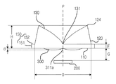
図1は、本実施形態に係る光学レンズの概略断面図である。 FIG. 1 is a schematic cross-sectional view of an optical lens according to the present embodiment.
光学レンズ100は、第1面110、第2面120、及び第3面130を含んでも良い。
The
つまり、前記光学レンズ100は、光が入射される第1面110と、前記第1面110と連結されて、前記第1面110に入射された光を反射させる第2面120と、前記第2面120に連結されて中央部に行くほど狭く陥没して、前記第1面110に入射された光を反射させる第3面130と、を含み、前記第2面120で反射された光は、前記第3面130で屈折されて出射されて、前記第3面130で反射された光は、前記第2面120で屈折されて出射されてもよい。
That is, the
前記第1面110には発光素子200から発生した光が入射されてもよい。尚、図1の実施形態で、前記第1面110は平面であってもよい。
Light generated from the
前記第2面120は、前記第1面110と連結されて、曲面または平面で形成されて、前記第2面120は、前記第1面110に対し傾斜するように形成されてもよい。前記第2面120では、前記第1面110に入射された光のうち大部分の光が出射されてもよい。
The
前記第2面120が、前記第1面110に対し傾斜するように形成されたのは、前記第1面110を介して入射された光の一部を前記第2面120から反射するようにして、光学レンズ100の高さと体積を減少及び光学レンズ100から出射された光の輝度均一性を向上させるためである。
The reason why the
前記第3面130は、第2面120に連結されて、前記第1面110と向き合うように形成されてもよい。
The
前記第3面130は、中央部に行くほど狭く陥没する形状で形成されて、第3面130は断面視で曲面で形成されてもよい。
The
この時、前記第3面130は、図1を参照すると、発光素子200の光軸(P)に行くほど狭く陥没する形状で形成されて、前記第3面130は、断面視で曲面で形成されてもよい。
At this time, referring to FIG. 1, the
このため、前記第2面120で反射された光は、前記第3面130で屈折されて光学レンズ100の外部に出射されて、‘B’経路に進み、前記第3面130で反射された光は、前記第2面120で屈折されて光学レンズ100の外部に出射されて、‘A’経路に進む。
For this reason, the light reflected by the
ここで、‘A’経路に進む光と‘B’経路に進む光は、互いに反対方向に進み、光量比が4:1〜1:4であってもよい。 Here, the light traveling on the ‘A’ path and the light traveling on the ‘B’ path may travel in opposite directions, and the light amount ratio may be 4: 1 to 1: 4.
尚、本実施形態は、‘A’経路に進む光の延長線と‘B’経路に進む光が、互いに20度以内の角(θ)を有することが好ましく、これは光学レンズの下部に反射面があるバックライトユニット(Back light unit、BLU)構造において、反射面を介してレンズ上部に光が進み暗部を無くすことができ、指向角の幅を減少させてより広い照度面を形成する。 In this embodiment, it is preferable that the extension line of the light traveling on the “A” path and the light traveling on the “B” path have an angle (θ) within 20 degrees, which is reflected on the lower part of the optical lens. In a backlight unit (BLU) structure having a surface, light can travel to the upper part of the lens through the reflection surface to eliminate the dark portion, and the width of the directivity angle can be reduced to form a wider illuminance surface.
ここで、前記‘A’経路に進む光の延長線と‘B’経路に進む光が、互いに20度を外れる場合、暗部が残存されて、光学特性が低下する。 Here, when the extension line of the light traveling on the ‘A’ path and the light traveling on the ‘B’ path deviate from each other by 20 degrees, the dark portion remains and the optical characteristics are deteriorated.
また、本実施形態の光学レンズは、下部面(第1面)に入射された光が、上面(第3面)で反射して側面(第2面)に屈折して進む経路と、側面で反射して上面で屈折して進む経路を有するため、バックライトユニットに適用時照度面の均一度を向上させることができる。 In the optical lens of the present embodiment, the light incident on the lower surface (first surface) is reflected by the upper surface (third surface) and refracted to the side surface (second surface). Since it has a path to be reflected and refracted on the upper surface, it is possible to improve the uniformity of the illuminance surface when applied to the backlight unit.
参考として、図1及び図3の‘150’は、射出及び組み立てのための鍔である。鍔150は、前記第2方向に前記第1面110から延びる第4面151と、前記第2面120に向かって前記第4面151から延びる第5面152をさらに含んでも良い。
For reference, reference numeral “150” in FIGS. 1 and 3 is a bag for injection and assembly. The
前記第1及び第4面110、151と、前記第4及び第5面151、152、並びに前記第2及び第5面120、152は、レンズの周面で連結されてもよい。
The first and
また、前記第4面151は、前記光軸(P)に対して光学レンズ100の最外側面で備えられても良い。
The
図2a乃至図2cは、本実施形態の光学レンズの一部断面図で、図3は、本実施形態の光学レンズに突出部が形成された断面図である。 2A to 2C are partial cross-sectional views of the optical lens of the present embodiment, and FIG. 3 is a cross-sectional view in which a protrusion is formed on the optical lens of the present embodiment.
光学レンズの側面である第2面120は、図2aのように凹状の曲面、図2cのように、凸状の曲面、図2bのように平面のうち一つであってもよい。
The
この時、図2bに示された通り、前記第2面120が平面の場合、前記第2面120は、第1面110に対し所定角度(θ’)だけ傾斜している。
At this time, as shown in FIG. 2 b, when the
尚、本実施形態の光学レンズは、第1面110に入射される光が光学レンズに分布することを制御できる突出部300が前記第1面110に形成されている。
In the optical lens of this embodiment, the
図3を参照すると、前記突出部300は、前記第1面110に形成されて、光学レンズの第2面120で反射された光が、第3面130で屈折されて出射される光量と、前記第3面130で反射された光が前記第2面120で屈折されて出射される光量を調節することができるように、光学レンズに入射された光の分布を調節するものである。
Referring to FIG. 3, the
従って、光学レンズで光分布を多様に調節するために、前記突出部300の形状は多様にすることができる。
ここで、前記突出部300は、前記第1面110から突出した形状であってもよい。
Accordingly, in order to adjust the light distribution with the optical lens, the shape of the
Here, the
一実施形態よると、前記突出部300は、図3に示された通り、中央が凹状に形成されてもよい。この時、前記第3面130の中心と前記突出部300の中心との間の距離をFとすると、突出部300は次の式を満たすことができる。
![]()
![]()
ここで、Hは本実施形態に係る光学レンズ100の高さである。
Here, H is the height of the
また、前記第3面130の中心の凹状の深さ(H−F)は、光学レンズ100の射出のための工程環境により変わるが、突出部300の中心と第3面130の中心が互いに触れ合ったり、この部分が孔で形成されることも可能である。
The concave depth (HF) at the center of the
前記突出部300は、前記第2及び第3面120、130に入射する発光素子200の光の分布を制御するためのものであるため、発光素子200の光の種類によって曲律が可変する。例えば、前記突出部300の中央は、図3のように凹状に形成できるが、発光素子200がLEDとして備えられる場合、前記突出部300の凹状の中央の深さは、次の式を満たすことができる。
![]()
![]()
この時、Dは鍔150(図1参照)を除いた第1面110の径である。
At this time, D is the diameter of the
一方、前記突出部300の厚さも、発光素子200の種類によって変わるが、これは前記第1面110の曲律により決定可能である。また、図示しないが前記突出部300の両終端は、前記発光素子200が設置された位置に向かって延びて形成されて、支持部材として用いても良い。この場合、図8に示された通り別の支持部材111を備える必要はなく、突出部300の両終端などが回路基板500(図8参照)に接触して前記第1面110と発光素子200を一定距離(G)離隔配置してもよい。
Meanwhile, the thickness of the
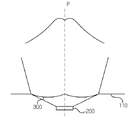
図4aと図4bは、本実施形態の突出部300が形成された光学レンズ100で光分布が変化するのを説明するための図面であり、図5は、本実施形態により突出部300が形成された光学レンズ100の光プロファイルを示した図面であり、図6a乃至図6fは、本実施形態の光学レンズ100に適用された突出部300の形状を説明するための一部断面図である。
4A and 4B are diagrams for explaining the change of light distribution in the
前述された通り、本実施形態の光学レンズ100は、突出部300が形成されていて、光学レンズ100の内部に適切な光分布を維持できるため、光学レンズ100から出射される光を制御することができる。
As described above, the
図4aは、第1面110に突出部が形成されていない図面で、発光素子200から出射された光は、第1面110を通過して光学レンズ100で光軸(P)がピーク(Peak)であるガウシアン(gaussian)光分布を示す。
FIG. 4 a is a drawing in which no protrusion is formed on the
この時、図4bに示された通り、前記第1面110に突出部300を形成すると、前記発光素子200から出射された光は、前記突出部300により、前記光学レンズ100で光軸(P)が凹状の光分布を示す。
At this time, as shown in FIG. 4 b, when the
このため、本実施形態の光学レンズ100は、突出部300の形状を変更することによって、入射された光に対し多様な光分布を有することができる。
For this reason, the
例えば、図5のように、第2面120で反射された光が、前記第3面130で屈折されて出射されて、光学レンズ100の上部を横切る‘B’の経路を有するようにして、前記第3面130で反射された光が、前記第2面120で屈折されて光学レンズ100の側面方向に出射される‘A’経路に行けるように、第1面110に形成された突出部300は助けを与えることができる。
For example, as shown in FIG. 5, the light reflected by the
また、前記突出部300は、‘A’経路に進む光と‘B’経路に進む光の光量比が、4:1〜1:4になるように調節することができる。
In addition, the
つまり、前記突出部300の形状を異ならせると、前記光学レンズ100内部での光分布が異なり、4:1〜1:4の光量比の範囲を前記突出部300の形状に調節することができる。
That is, if the shape of the
例えば、‘A’経路に進む光と‘B’経路に進む光の光量比が4:1である場合の突出部300の形状と前記光量比が1:4である突出部300の形状は異なる。
For example, the shape of the
したがって、前記突出部300を介して入射された光は、前記第3面130で反射されて第2面120で屈折される光と前記第2面120で反射されて前記第3面130で屈折される光の光量比が4:1〜1:4であってもよい。
Accordingly, the light incident through the
このように、本実施形態の光学レンズ100に適用された突出部300の形状を図6a乃至図6fを参照して説明すると、まず、第1面110から発光素子200方向(光入射される方向(E)の反対方向)に突出した形状を有する突出部「310」(図6a)を構成することができ、前記第1面110から発光素子200方向の反対方向(光入射方向(E))で突出した形状(すなわち、前記第1面110でぼこぼこした形状)を有する突出部「310」(図6b)を構成することができる。
As described above, the shape of the
そして、図6aの突出した形状の突出部「310」で、光入射方向に少なくとも一つの凹部が形成されることができて、図6cは、一つの凹部311aが形成された突出部「311」を示し、この一つの凹部311aの中心は光軸(P)と一致することができる。
6a, at least one recess may be formed in the light incident direction, and FIG. 6c illustrates a protrusion “311” having one
また、図6dは、二つの凹部312a、312bが形成されている突出部「312」を示し、この二つの凹部312a、312bは、光軸(P)と一致しない。
FIG. 6d shows a protrusion “312” in which two
さらに、前述された図6a乃至図6dの突出部310、311、312は、曲面で形成されているが、図6e及び図6fは、第1面110から断面が三角形の突出部に突出部「313」と「315」を形成する。
Further, the
つまり、図6eは、第1面110から断面が三角形の突出部が一つで、断面上で、第1直線313aと第2直線313bの合からなり、第1直線313aと第2直線313bが交差する三角形頂点313cは、光軸(P)と一致する。
That is, FIG. 6E shows that the
そして、図6fは、第1面110から断面が三角形の二つの突出部315a、315bで突出部「315」を形成したものである。
In FIG. 6F, a protrusion “315” is formed by two
一方、本実施形態の突出部は、光軸に対して対称にされた形状であってもよい。 On the other hand, the protrusion of the present embodiment may have a shape that is symmetric with respect to the optical axis.
図7は、本実施形態に係る光照射装置を示した概略断面図で、図8は、本実施形態に係る光照射装置の発光素子と光学レンズが組み立てられた一例を示した一部断面図である。 FIG. 7 is a schematic cross-sectional view illustrating the light irradiation apparatus according to the present embodiment, and FIG. 8 is a partial cross-sectional view illustrating an example in which the light emitting element and the optical lens of the light irradiation apparatus according to the present embodiment are assembled. It is.
本実施形態に係る光照射装置は、光学レンズ100、回路基板500、及び発光素子200を含んでも良い。
The light irradiation apparatus according to this embodiment may include the
つまり、本実施形態に係る光照射装置は、回路基板500と、前記回路基板500に実装された複数の発光素子200と、前記複数の発光素子200各々に対応されて前記回路基板500に組み立てられている光学レンズ100と、を含んでも良い。
That is, the light irradiation apparatus according to the present embodiment is assembled to the
前記回路基板500は、短辺より長辺が長い長方形プレート形状で形成されてもよく、前記発光素子200には回路パターン(図示せず)が形成されて、回路パターンは、前記発光素子200に駆動信号を伝達する。
The
そして、前記発光素子200は、前記回路基板500の回路パターンに電気的に連結されて回路パターンに認可された駆動信号によって光を発生させる。
The
前記発光素子200から発生した光は360度方向で特定指向角でファジーは光プロファイルを有し、前記発光素子200から発生した光は高輝度特性を有する反面輝度均一性は大きく落ちる光プロファイルを有する。
The light generated from the
これと共に高輝度特性を有する反面輝度均一性が大きく減少される光プロファイルを有する発光素子200の輝度均一性を改善するために各発光素子200には光学レンズ100が配置されてもよい。
At the same time, an
前述された通り、前記光学レンズ100は第1面110、第2面及び第3面を含んでも良い。
As described above, the
前記光学レンズ100は、前記発光素子200から発生された光をより効率的に拡散させるために、前記発光素子200から発生した光の一部は、前記第1面110に入射されて前記第2面から前記第3面に反射して、前記第3面で屈折されて前記光学レンズ100の外部に出射されて、前記発光素子200から発生した光の一部は、前記第3面から前記第2面に反射されて、前記第2面で屈折されて前記光学レンズ100の外部に出射されることができる。
In order for the
このように光学レンズ100を利用して、光の輝度均一性を大きく向上させられ、より少ない個数の発光素子200を利用して、高輝度及び高い輝度均一性を有する光プロファイルを形成できるだけでなく消費電力をより減少させることができる。
As described above, the
尚、本実施形態では、前記光学レンズ100が前記発光素子200から所定間隔(d)離隔されている。
In the present embodiment, the
一方、本実施形態の光照射装置は、回路基板500に複数の発光素子200が配列されて、複数の発光素子200各々に光学レンズ100が組み立てられている。
On the other hand, in the light irradiation apparatus of this embodiment, a plurality of
この時、図7のように、複数の発光素子「201」、「202」、「203」、「204」が、前記回路基板500に配列されているが、複数の発光素子「201」、「202」、「203」、「204」各々は、発光輝度及び出射される光分布が同じであってもいいが、光照射装置の適用される装置で発光輝度及び出射される光分布を異ならせてもよい。
At this time, as shown in FIG. 7, a plurality of light emitting elements “201”, “202”, “203”, and “204” are arranged on the
したがって、前記複数の発光素子「201」、「202」、「203」、「204」各々に組み立てられている光学レンズ「101」、「102」、「103」、「104」から出射される光の輝度及び出射される光分布が異なるように設計されて、前記複数の発光素子「201」、「202」、「203」、「204」各々に対応した前記光学レンズ「101」、「102」、「103」、「104」が互いに異なる経路に光を出射させるように設計されることができる。 Therefore, light emitted from the optical lenses “101”, “102”, “103”, “104” assembled in each of the plurality of light emitting elements “201”, “202”, “203”, “204”. The optical lenses “101” and “102” corresponding to the plurality of light emitting elements “201”, “202”, “203”, and “204” are designed so as to have different luminance and emitted light distribution. , “103”, “104” can be designed to emit light to different paths.
ここで、前記光学レンズ「101」、「102」、「103」、「104」から出射される輝度及び出射される光分布が同じであってもよい。 Here, the brightness emitted from the optical lenses “101”, “102”, “103”, and “104” and the emitted light distribution may be the same.
そこで、前記光学レンズ「101」、「102」、「103」、「104」は、光学レンズの第3面130で反射されて第2面120で屈折される光と前記第2面120で反射されて前記第3面130で屈折される光の光量比は異なることもある。
Therefore, the optical lenses “101”, “102”, “103”, “104” are reflected by the
この光量比は前述された通り、4:1〜1:4であってもよい。 This light quantity ratio may be 4: 1 to 1: 4 as described above.
さらに、前記光学レンズ「101」、「102」、「103」、「104」は、前記複数の発光素子200各々に対応されて前記回路基板500に組み立てられるが、図8のように、前記光学レンズ「101」、「102」、「103」、「104」にレッグ(leg)111を形成して、前記光学レンズ「101」、「102」、「103」、「104」は、前記支持部材111を利用して前記回路基板500に実装される。
Further, the optical lenses “101”, “102”, “103”, and “104” are assembled to the
図9は、本実施形態に係るバックライトユニットを説明するための概念図である。 FIG. 9 is a conceptual diagram for explaining the backlight unit according to the present embodiment.
図9に示された照明装置は、図7に示された光照射装置と実質的に同じ構成を有する。したがって、同じ構成に対する重複した説明は省略して、同じ構成に対しては同じ名称及び同じ参照符号を付与することにする。 The illuminating device shown in FIG. 9 has substantially the same configuration as the light irradiation device shown in FIG. Therefore, the duplicate description with respect to the same structure is abbreviate | omitted, and will give the same name and the same referential mark with respect to the same structure.
図9を参照すると、照明装置は、光照射装置250、光学シート600を含んでも良い。
Referring to FIG. 9, the illumination device may include a
前記光学シート600は、バックライトユニットのような照明装置を構成する一般的な構成であるため、その説明は省略して、例えば、拡散フィルムを含む複数の光学フィルム610、620、630で構成されてもよい。
Since the
尚、前記光照射装置250の上部に前記光学シート600が配置されてもよい。
The
さらに、本実施形態に係るバックライトユニットは、ボトムケース(図示せず)及び反射版(図示せず)を含んでも良い。
例えば、ボトムケースは、底板に反射版を配置して、反射版は光照射装置250の光学レンズ100から出射された光を反射させる役割を果たす。
Furthermore, the backlight unit according to the present embodiment may include a bottom case (not shown) and a reflective plate (not shown).
For example, the bottom case has a reflection plate disposed on the bottom plate, and the reflection plate plays a role of reflecting light emitted from the
本実施形態は具体的な例に対してのみ詳細に説明されたが、本発明の技術思想範囲内で多様な変形及び修正が可能であることは、当業者にとって明白であり、このような変形及び修正が、添付された特許請求範囲に属することは当然である。 Although the present embodiment has been described in detail only with respect to a specific example, it is obvious to those skilled in the art that various changes and modifications can be made within the scope of the technical idea of the present invention. Naturally, modifications and variations are within the scope of the appended claims.
100 光学レンズ
200 発光素子
250 光照射装置
300 突出部
500 回路基板
600 光学シート
610、620、630 光学フィルム
DESCRIPTION OF
Claims (18)
前記第1面と連結されて、前記第1面から上方方向に延びる第2面と、
前記第2面と連結されて、中心が前記第1面に向かって陥没して、前記中心と縁が曲面で連結されて、前記中心と前記第1面の中心を通過するように延びる直線である光軸方向に対称になるように曲線状に前記第1面と離隔配置される第3面と、
前記光軸と中心整列されて、前記第1面に対し前記光軸に沿って前記第3面から遠くなる第1方向に突出形成されて、断面が光軸に対して対称な二つの曲線部を形成して、各々の曲線部は、前記第1方向に突出して、前記複数の曲線部が連結される部分は前記光軸に沿って前記第1方向の反対方向で前記第3面と近くなる第2方向の曲線を形成する突出部と、
前記第1面から前記第1方向に延びて形成されて、前記突出部の下空間に前記突出部と近接配置される複数の支持部材と、を含み、
前記第1面を介して入射されて前記第2面で反射される光は前記第3面で屈折されて出射され、
前記第1面を介して入射されて前記第3面で反射される光は前記第2面で屈折されて出射され、
前記第2面で屈折されて出射される光と前記第3面で屈折されて出射される光の方向は反対であることを特徴とする光学レンズ。 The first side,
A second surface connected to the first surface and extending upward from the first surface;
A straight line that is connected to the second surface, the center is depressed toward the first surface, the center and the edge are connected by a curved surface, and extends so as to pass through the center and the center of the first surface. A third surface spaced apart from the first surface in a curved shape so as to be symmetric in a certain optical axis direction;
Two curved portions that are aligned with the optical axis and project in the first direction away from the third surface along the optical axis with respect to the first surface, and whose cross sections are symmetrical with respect to the optical axis Each of the curved portions protrudes in the first direction, and a portion where the plurality of curved portions are connected is close to the third surface in the direction opposite to the first direction along the optical axis. a protrusion forming a second direction of the curve becomes,
Is formed to extend in the first direction from the first surface, seen including a plurality of support members wherein disposed close to the projecting portion below the space of the protrusion,
The light incident through the first surface and reflected by the second surface is refracted and emitted from the third surface;
The light incident through the first surface and reflected by the third surface is refracted and emitted from the second surface;
An optical lens, wherein directions of light refracted and emitted by the second surface and light refracted and emitted by the third surface are opposite to each other .
前記第2面に向かって前記第4面から延びる第5面と、をさらに含むことを特徴とする請求項1乃至3のうちいずれか一つに記載の光学レンズ。 A fourth surface extending from the first surface in the second direction;
The optical lens according to claim 1, further comprising a fifth surface extending from the fourth surface toward the second surface.
光軸に対して傾斜した状態で前記第1面から延びて形成されることを特徴とする請求項1乃至5のうちいずれか一つに記載の光学レンズ。 The second surface is
The optical lens according to claim 1, wherein the optical lens is formed to extend from the first surface in an inclined state with respect to the optical axis.
前記基板に配置される複数の発光素子と、
前記複数の発光素子各々を覆うことができるように各々の発光素子上に配置される複数の光学レンズと、を含み、
前記複数の光学レンズは、
第1面と、
前記第1面と連結されて、前記第1面から上方方向に延びる第2面と、
前記第2面と連結されて、中心が前記第1面に向かって陥没して、前記中心と縁が曲面で連結されて、前記中心と前記第1面の中心を通過するように延びる直線である光軸方向 に対称になるように曲線状に前記第1面と離隔配置される第3面と、
前記光軸と中心整列されて、前記第1面から前記光軸に沿って前記第3面から遠くなる第1方向に突出形成されて、断面が光軸に対して対称な二つの曲線部を形成して、各々の曲線部は前記第1方向に突出して、前記複数の曲線部が連結される部分は前記光軸に沿って前記第1方向の反対方向で前記第3面と近くなる第2方向の曲線を形成する突出部と、
前記第1面から前記第1方向に延びて形成されて、前記突出部の下空間に前記突出部と近接配置される複数の支持部材と、を含み、
前記第1面を介して入射されて前記第2面で反射される光は前記第3面で屈折されて出射され、
前記第1面を介して入射されて前記第3面で反射される光は前記第2面で屈折されて出射され、
前記第2面で屈折されて出射される光と前記第3面で屈折されて出射される光の方向は反対であることを特徴とする光発散装置。 A substrate,
A plurality of light emitting elements disposed on the substrate;
A plurality of optical lenses disposed on each light emitting element so as to cover each of the plurality of light emitting elements,
The plurality of optical lenses are:
The first side,
A second surface connected to the first surface and extending upward from the first surface;
A straight line that is connected to the second surface, the center is depressed toward the first surface, the center and the edge are connected by a curved surface, and extends so as to pass through the center and the center of the first surface. A third surface spaced apart from the first surface in a curved shape so as to be symmetric in a certain optical axis direction;
Two curved portions that are center-aligned with the optical axis and project from the first surface along the optical axis in a first direction far from the third surface , and whose cross-sections are symmetrical with respect to the optical axis. Each curved portion protrudes in the first direction, and a portion where the plurality of curved portions are connected is close to the third surface in the opposite direction of the first direction along the optical axis. A protrusion forming a curve in two directions;
Is formed to extend in the first direction from the first surface, seen including a plurality of support members wherein disposed close to the projecting portion below the space of the protrusion,
The light incident through the first surface and reflected by the second surface is refracted and emitted from the third surface;
The light incident through the first surface and reflected by the third surface is refracted and emitted from the second surface;
The light divergence device characterized in that the light refracted and emitted by the second surface is opposite to the light refracted and emitted by the third surface .
少なくとも一つ以上の前記光学シートと近接された位置に配置される光発散装置と、を含み、
前記光発散装置は、
基板と、
前記基板に配置される複数の発光素子と、
前記複数の発光素子各々を覆うことができるように各々の発光素子上に配置される複数の光学レンズと、を含み、
前記複数の光学レンズは、
第1面と、
前記第1面と連結されて、前記第1面から上方方向に延びる第2面と、
前記第2面と連結されて、中心が前記第1面に向かって陥没して、前記中心と縁が曲面で連結されて、前記中心と前記第1面の中心を通過するように延びる直線である光軸方向に対称になるように曲線状に前記第1面と離隔配置される第3面と、
前記光軸と中心整列されて、前記第1面から前記光軸に沿って前記第3面から遠くなる第1方向に突出形成されて、断面が光軸に対し対称な二つの曲線部を形成して、各々の曲線部は、前記第1方向に突出して、前記複数の曲線部が連結される部分は前記光軸に沿って前記第1方向の反対方向で前記第3面と近くなる第2方向の曲線を形成する突出部と、
前記第1面から前記第1方向に延びて形成されて、前記突出部の下空間に前記突出部と近接配置される複数の支持部材と、を含み、
前記第1面を介して入射されて前記第2面で反射される光は前記第3面で屈折されて出射され、
前記第1面を介して入射されて前記第3面で反射される光は前記第2面で屈折されて出射され、
前記第2面で屈折されて出射される光と前記第3面で屈折されて出射される光の方向は反対であることを特徴とする照明装置。 At least one optical sheet;
A light diverging device disposed at a position close to at least one of the optical sheets,
The light diverging device is
A substrate,
A plurality of light emitting elements disposed on the substrate;
A plurality of optical lenses disposed on each light emitting element so as to cover each of the plurality of light emitting elements,
The plurality of optical lenses are:
The first side,
A second surface connected to the first surface and extending upward from the first surface;
A straight line that is connected to the second surface, the center is depressed toward the first surface, the center and the edge are connected by a curved surface, and extends so as to pass through the center and the center of the first surface. A third surface spaced apart from the first surface in a curved shape so as to be symmetric in a certain optical axis direction;
Centered with the optical axis, is formed to protrude from the first surface along the optical axis in a first direction away from the third surface, and to form two curved sections whose cross sections are symmetrical with respect to the optical axis Then, each curved portion protrudes in the first direction, and a portion where the plurality of curved portions are connected is close to the third surface in the opposite direction of the first direction along the optical axis. A protrusion forming a curve in two directions;
Is formed to extend in the first direction from the first surface, seen including a plurality of support members wherein disposed close to the projecting portion below the space of the protrusion,
The light incident through the first surface and reflected by the second surface is refracted and emitted from the third surface;
The light incident through the first surface and reflected by the third surface is refracted and emitted from the second surface;
The direction of the light refracted and emitted by the second surface and the light refracted and emitted by the third surface are opposite to each other .
Applications Claiming Priority (2)
| Application Number | Priority Date | Filing Date | Title |
|---|---|---|---|
| KR10-2013-0033374 | 2013-03-28 | ||
| KR1020130033374A KR101524914B1 (en) | 2013-03-28 | 2013-03-28 | Light diffusion device, and light emitting device array unit having the same |
Publications (3)
| Publication Number | Publication Date |
|---|---|
| JP2014194545A JP2014194545A (en) | 2014-10-09 |
| JP2014194545A5 JP2014194545A5 (en) | 2017-05-18 |
| JP6286248B2 true JP6286248B2 (en) | 2018-02-28 |
Family
ID=50771032
Family Applications (1)
| Application Number | Title | Priority Date | Filing Date |
|---|---|---|---|
| JP2014068551A Active JP6286248B2 (en) | 2013-03-28 | 2014-03-28 | Optical lens, light irradiation device, and illumination device having the same |
Country Status (5)
| Country | Link |
|---|---|
| US (1) | US9995461B2 (en) |
| EP (1) | EP2784377B1 (en) |
| JP (1) | JP6286248B2 (en) |
| KR (1) | KR101524914B1 (en) |
| CN (1) | CN104075241B (en) |
Families Citing this family (9)
| Publication number | Priority date | Publication date | Assignee | Title |
|---|---|---|---|---|
| USD753746S1 (en) * | 2014-04-15 | 2016-04-12 | Hon Hai Precision Industry Co., Ltd. | Lens |
| US10411173B2 (en) * | 2015-03-31 | 2019-09-10 | Nichia Corporation | Light emitting device and light emitting module using the same |
| US10302278B2 (en) * | 2015-04-09 | 2019-05-28 | Cree, Inc. | LED bulb with back-reflecting optic |
| CN108027110B (en) * | 2015-09-01 | 2020-07-10 | Lg 伊诺特有限公司 | Lighting device |
| US10464472B2 (en) | 2016-11-18 | 2019-11-05 | Rebo Lighting & Electronics, Llc | Illumination assembly for a vehicle |
| US10578278B2 (en) * | 2017-06-05 | 2020-03-03 | Lumileds Holding B.V. | Optical lens for extremely thin direct-lit backlight |
| US11242977B2 (en) | 2017-07-26 | 2022-02-08 | Lumileds Llc | Illumination device with element having annular coating |
| KR102476140B1 (en) * | 2017-11-20 | 2022-12-09 | 삼성전자주식회사 | Optical device and light source module having the same |
| CN110111681A (en) * | 2019-04-08 | 2019-08-09 | 惠州市华星光电技术有限公司 | Backlight module preparation method and system |
Family Cites Families (50)
| Publication number | Priority date | Publication date | Assignee | Title |
|---|---|---|---|---|
| US6607286B2 (en) * | 2001-05-04 | 2003-08-19 | Lumileds Lighting, U.S., Llc | Lens and lens cap with sawtooth portion for light emitting diode |
| US6598998B2 (en) * | 2001-05-04 | 2003-07-29 | Lumileds Lighting, U.S., Llc | Side emitting light emitting device |
| US6679621B2 (en) | 2002-06-24 | 2004-01-20 | Lumileds Lighting U.S., Llc | Side emitting LED and lens |
| US6974229B2 (en) | 2003-05-21 | 2005-12-13 | Lumileds Lighting U.S., Llc | Devices for creating brightness profiles |
| TWI249257B (en) | 2004-09-24 | 2006-02-11 | Epistar Corp | Illumination apparatus |
| JP2006093470A (en) | 2004-09-24 | 2006-04-06 | Toshiba Corp | Lead frame, light-emitting device, and manufacturing method thereof |
| KR101080355B1 (en) | 2004-10-18 | 2011-11-04 | 삼성전자주식회사 | Light emitting diode, lens for the same |
| DE102005019832A1 (en) | 2005-02-28 | 2006-09-14 | Osram Opto Semiconductors Gmbh | Illumination device for LCD-display device, has auxiliary component designed as optical component and inserted into recess in optical unit, where component is connected with optical unit in connection region in mechanically stable manner |
| KR100660721B1 (en) * | 2005-04-26 | 2006-12-21 | 엘지전자 주식회사 | Lens for side light emitting and light emitting device using the lens |
| KR100661719B1 (en) | 2005-04-26 | 2006-12-26 | 엘지전자 주식회사 | Lens for side light emitting and package using the lens |
| JP2006309242A (en) * | 2005-04-26 | 2006-11-09 | Lg Electronics Inc | Optical lens, light emitting element package using same, and backlight unit |
| TWI260380B (en) * | 2005-08-05 | 2006-08-21 | Chi Lin Technology Co Ltd | Lens for LED |
| JP5094951B2 (en) | 2005-11-11 | 2012-12-12 | 株式会社ジャパンディスプレイイースト | Liquid crystal display |
| JP4702539B2 (en) | 2005-11-16 | 2011-06-15 | 日亜化学工業株式会社 | Optical member and light source device using the same |
| KR100713582B1 (en) | 2005-12-20 | 2007-05-02 | 서울반도체 주식회사 | High-efficiency led for key pads |
| WO2008007492A1 (en) * | 2006-07-11 | 2008-01-17 | Koha Co., Ltd. | Light source module, surface area light-emitting unit, and surface area light-emitting device |
| KR101221066B1 (en) | 2006-10-30 | 2013-02-12 | 삼성전자주식회사 | Side emitting lens, backlight unit and liquid crystal display having the same |
| TW200827617A (en) * | 2006-12-20 | 2008-07-01 | Ind Tech Res Inst | Lens cap and light emitting diode package using the same |
| JP4799433B2 (en) | 2007-01-31 | 2011-10-26 | 株式会社小糸製作所 | Vehicle lighting |
| US7837349B2 (en) * | 2007-06-15 | 2010-11-23 | Visteon Global Technologies, Inc. | Near field lens |
| US7703950B2 (en) * | 2007-11-21 | 2010-04-27 | C-R Control Systems, Inc. | Side-emitting lens for LED lamp |
| KR20110025896A (en) | 2008-06-23 | 2011-03-14 | 파나소닉 주식회사 | Light emitting apparatus, planar light emitting apparatus and display apparatus |
| JP5030938B2 (en) * | 2008-12-26 | 2012-09-19 | 三菱電機株式会社 | Lens, light source device and lighting device |
| TW201025661A (en) * | 2008-12-26 | 2010-07-01 | Univ Chung Yuan Christian | Side view LED (light emitting diode) module |
| JP2011018863A (en) | 2009-07-10 | 2011-01-27 | Sharp Corp | Light-emitting element module, method of manufacturing the same, and backlight apparatus |
| TW201120377A (en) | 2009-07-22 | 2011-06-16 | Teijin Ltd | Led illuminator |
| JP5264650B2 (en) * | 2009-08-21 | 2013-08-14 | スタンレー電気株式会社 | LED lighting device |
| JP5719104B2 (en) | 2009-08-24 | 2015-05-13 | 株式会社エンプラス | Light flux controlling member, light emitting device, surface light source device, and display device |
| USD632834S1 (en) * | 2009-10-30 | 2011-02-15 | Teijin Limited | Lens for a light emitting diode lamp |
| WO2011055467A1 (en) * | 2009-11-04 | 2011-05-12 | ナルックス株式会社 | Lighting device |
| JP5493147B2 (en) * | 2010-04-07 | 2014-05-14 | 株式会社エンプラス | Luminous flux control member, light emitting device, and illumination device |
| KR101047439B1 (en) | 2010-04-09 | 2011-07-08 | 엘지이노텍 주식회사 | Lens and lighting unit comprising lens |
| US9157602B2 (en) * | 2010-05-10 | 2015-10-13 | Cree, Inc. | Optical element for a light source and lighting system using same |
| KR101668262B1 (en) | 2010-06-22 | 2016-10-21 | 엘지디스플레이 주식회사 | Light emitting diode and method of fabricating the same |
| JPWO2012004975A1 (en) * | 2010-07-07 | 2013-09-02 | パナソニック株式会社 | Light distribution control device, light emitting device using the same, and method for manufacturing light distribution control device |
| EP2646747A1 (en) * | 2010-11-30 | 2013-10-09 | Koninklijke Philips N.V. | Light redirecting and diffusing module for light emitting diodes |
| FR2973476A1 (en) * | 2011-03-31 | 2012-10-05 | Valeo Vision | OPTICAL SYSTEM FOR GENERATING A COMPOSITE LARGE BEAM OF LARGE ANGULAR OPENING |
| JP6025309B2 (en) | 2011-06-29 | 2016-11-16 | シャープ株式会社 | Light source device and liquid crystal display device |
| JP5764407B2 (en) * | 2011-06-30 | 2015-08-19 | 株式会社エンプラス | Luminous flux control member, light emitting device, and surface light source device |
| KR20130003853A (en) | 2011-07-01 | 2013-01-09 | 정대일 | Lighting apparatus using light emitting diode |
| TWI412706B (en) | 2011-07-27 | 2013-10-21 | 麗光科技股份有限公司 | Light source module using the same |
| KR101957184B1 (en) * | 2011-12-02 | 2019-03-13 | 엘지전자 주식회사 | Backlight unit and display apparatus having the same |
| US10047930B2 (en) * | 2011-12-02 | 2018-08-14 | Seoul Semiconductor Co., Ltd. | Light emitting module and lens |
| EP2786428B1 (en) * | 2011-12-02 | 2023-07-12 | Seoul Semiconductor Co., Ltd. | Light emitting module and lens |
| KR101287023B1 (en) | 2012-02-13 | 2013-07-17 | (주)엔디에스 | Diffusion lens for illumination and back light |
| TW201408946A (en) * | 2012-08-21 | 2014-03-01 | 辰峯光電股份有限公司 | Light emitting apparatus |
| US20150285463A1 (en) * | 2012-10-19 | 2015-10-08 | Koninklijke Philips N.V. | Lighting device for indirect illumination having prism elements |
| US9134007B2 (en) * | 2012-11-06 | 2015-09-15 | Darwin Precisions Corporation | Light source device |
| KR101299528B1 (en) * | 2012-12-18 | 2013-08-23 | (주)애니캐스팅 | Side emitting light emitting diode lens, back light unit and display device including the same |
| CN103471009A (en) * | 2013-09-13 | 2013-12-25 | 东莞市欧科光电科技有限公司 | Novel LED lens and liquid crystal display backlight screen |
-
2013
- 2013-03-28 KR KR1020130033374A patent/KR101524914B1/en not_active IP Right Cessation
-
2014
- 2014-03-28 CN CN201410123967.9A patent/CN104075241B/en active Active
- 2014-03-28 EP EP14162193.8A patent/EP2784377B1/en active Active
- 2014-03-28 JP JP2014068551A patent/JP6286248B2/en active Active
- 2014-03-28 US US14/228,502 patent/US9995461B2/en active Active
Also Published As
| Publication number | Publication date |
|---|---|
| EP2784377A1 (en) | 2014-10-01 |
| EP2784377B1 (en) | 2023-05-24 |
| KR101524914B1 (en) | 2015-06-01 |
| US20140293582A1 (en) | 2014-10-02 |
| CN104075241A (en) | 2014-10-01 |
| US9995461B2 (en) | 2018-06-12 |
| JP2014194545A (en) | 2014-10-09 |
| KR20140118092A (en) | 2014-10-08 |
| CN104075241B (en) | 2020-10-02 |
Similar Documents
| Publication | Publication Date | Title |
|---|---|---|
| JP6286248B2 (en) | Optical lens, light irradiation device, and illumination device having the same | |
| CN107255886B (en) | Planar lighting device and display device | |
| TWI466319B (en) | A light emitting device, a lighting device, and a display device | |
| TWI467118B (en) | A light emitting device, a lighting device, and a display device | |
| JP5276306B2 (en) | System for improving backlight illumination uniformity | |
| JP5509154B2 (en) | Light emitting device and display device | |
| KR101299529B1 (en) | Lens for light emitting diode, back light unit and display device including the same | |
| KR20060048281A (en) | Liquid crystal display device and backlight module thereof | |
| TWI640819B (en) | Backlight module | |
| JP6310285B2 (en) | Light emitting device, surface light source device, and display device | |
| KR101419031B1 (en) | Light emitting device and lighting device having the same | |
| JP5766044B2 (en) | Luminous flux control member, light emitting device including the luminous flux control member, and surface light source device including the light emitting device | |
| KR101408324B1 (en) | Led lens for wide diffusion light | |
| TWI506229B (en) | Light emitting apparatus and lens | |
| JP2006201642A (en) | Diffusion lens array sheet and surface light source device | |
| JP2020088382A (en) | Light diffusing lens for light emitting element | |
| US20090147533A1 (en) | Display Device | |
| JP2018137053A (en) | Luminous flux control member, light-emitting device, and surface light source device | |
| JP2014225322A (en) | Surface light source device, display device, and lighting device | |
| KR101901317B1 (en) | Lens for wide diffusion light | |
| KR101921180B1 (en) | Planar lighting device and display device using the same | |
| WO2013089172A1 (en) | Light source device, planar light source device, display device, and illumination device | |
| KR102031549B1 (en) | Light diffusion device, and light emitting device array unit having the same | |
| JP4604125B2 (en) | Surface light source device | |
| JP2017091939A (en) | Surface light source device and liquid crystal display device |
Legal Events
| Date | Code | Title | Description |
|---|---|---|---|
| A521 | Request for written amendment filed |
Free format text: JAPANESE INTERMEDIATE CODE: A523 Effective date: 20170327 |
|
| A621 | Written request for application examination |
Free format text: JAPANESE INTERMEDIATE CODE: A621 Effective date: 20170327 |
|
| A977 | Report on retrieval |
Free format text: JAPANESE INTERMEDIATE CODE: A971007 Effective date: 20170920 |
|
| A131 | Notification of reasons for refusal |
Free format text: JAPANESE INTERMEDIATE CODE: A131 Effective date: 20170926 |
|
| A521 | Request for written amendment filed |
Free format text: JAPANESE INTERMEDIATE CODE: A523 Effective date: 20171214 |
|
| TRDD | Decision of grant or rejection written | ||
| A01 | Written decision to grant a patent or to grant a registration (utility model) |
Free format text: JAPANESE INTERMEDIATE CODE: A01 Effective date: 20180109 |
|
| A61 | First payment of annual fees (during grant procedure) |
Free format text: JAPANESE INTERMEDIATE CODE: A61 Effective date: 20180205 |
|
| R150 | Certificate of patent or registration of utility model |
Ref document number: 6286248 Country of ref document: JP Free format text: JAPANESE INTERMEDIATE CODE: R150 |
|
| R250 | Receipt of annual fees |
Free format text: JAPANESE INTERMEDIATE CODE: R250 |
|
| R250 | Receipt of annual fees |
Free format text: JAPANESE INTERMEDIATE CODE: R250 |
|
| R250 | Receipt of annual fees |
Free format text: JAPANESE INTERMEDIATE CODE: R250 |
|
| R250 | Receipt of annual fees |
Free format text: JAPANESE INTERMEDIATE CODE: R250 |